EP2768286A2 - Dispositif d'éclairage et accessoire d'éclairage - Google Patents
Dispositif d'éclairage et accessoire d'éclairage Download PDFInfo
- Publication number
- EP2768286A2 EP2768286A2 EP14155361.0A EP14155361A EP2768286A2 EP 2768286 A2 EP2768286 A2 EP 2768286A2 EP 14155361 A EP14155361 A EP 14155361A EP 2768286 A2 EP2768286 A2 EP 2768286A2
- Authority
- EP
- European Patent Office
- Prior art keywords
- temperature
- control circuit
- lighting device
- light source
- temperature control
- Prior art date
- Legal status (The legal status is an assumption and is not a legal conclusion. Google has not performed a legal analysis and makes no representation as to the accuracy of the status listed.)
- Granted
Links
- 238000001514 detection method Methods 0.000 claims abstract description 102
- 238000000034 method Methods 0.000 claims abstract description 43
- 239000007787 solid Substances 0.000 claims abstract description 32
- 230000003247 decreasing effect Effects 0.000 claims abstract description 28
- 230000007423 decrease Effects 0.000 claims description 69
- 238000001816 cooling Methods 0.000 claims description 18
- 239000000758 substrate Substances 0.000 claims description 14
- 230000005856 abnormality Effects 0.000 description 20
- 238000010586 diagram Methods 0.000 description 20
- 230000000694 effects Effects 0.000 description 7
- 230000006866 deterioration Effects 0.000 description 6
- 238000009529 body temperature measurement Methods 0.000 description 5
- 230000017525 heat dissipation Effects 0.000 description 5
- 239000003990 capacitor Substances 0.000 description 3
- 239000004065 semiconductor Substances 0.000 description 2
- 238000004804 winding Methods 0.000 description 2
- 235000010724 Wisteria floribunda Nutrition 0.000 description 1
- 230000032683 aging Effects 0.000 description 1
- 239000002826 coolant Substances 0.000 description 1
- 238000009434 installation Methods 0.000 description 1
- 239000007788 liquid Substances 0.000 description 1
- 238000004377 microelectronic Methods 0.000 description 1
Images






Classifications
-
- H—ELECTRICITY
- H05—ELECTRIC TECHNIQUES NOT OTHERWISE PROVIDED FOR
- H05B—ELECTRIC HEATING; ELECTRIC LIGHT SOURCES NOT OTHERWISE PROVIDED FOR; CIRCUIT ARRANGEMENTS FOR ELECTRIC LIGHT SOURCES, IN GENERAL
- H05B45/00—Circuit arrangements for operating light-emitting diodes [LED]
- H05B45/50—Circuit arrangements for operating light-emitting diodes [LED] responsive to malfunctions or undesirable behaviour of LEDs; responsive to LED life; Protective circuits
- H05B45/56—Circuit arrangements for operating light-emitting diodes [LED] responsive to malfunctions or undesirable behaviour of LEDs; responsive to LED life; Protective circuits involving measures to prevent abnormal temperature of the LEDs
-
- H—ELECTRICITY
- H05—ELECTRIC TECHNIQUES NOT OTHERWISE PROVIDED FOR
- H05B—ELECTRIC HEATING; ELECTRIC LIGHT SOURCES NOT OTHERWISE PROVIDED FOR; CIRCUIT ARRANGEMENTS FOR ELECTRIC LIGHT SOURCES, IN GENERAL
- H05B45/00—Circuit arrangements for operating light-emitting diodes [LED]
- H05B45/10—Controlling the intensity of the light
Definitions
- the present invention relates to lighting devices and lighting fixtures using the same, and particularly to a lighting device for solid state light emitting devices such as light emitting diodes and a lighting fixture using the same.
- An LED lighting apparatus disclosed in document 1 includes a lighting body and a liquid-cooled heat dissipation mechanism.
- the lighting body includes an LED light source, a temperature detection device, and a water-cooling jacket for cooling the LED light source.
- the liquid-cooled heat dissipation mechanism cools, by use of a radiator, a liquid coolant which absorbs heat from the LED light source when passing through the water-cooling jacket.
- the LED light source is operated by use of a control current corresponding to a detection temperature from the temperature detection device.
- the present invention has aimed to propose a lighting device capable of suppressing an increase in a temperature of a solid state light emitting device to avoid that the temperature of the solid state light emitting device exceeds an allowable temperature, and a lighting fixture using the same.
- the lighting device of the first aspect in accordance with the present invention includes a power supply circuit, a temperature detection circuit, and a temperature control circuit.
- the power supply circuit is configured to supply operation power to a light source including a solid state light emitting device.
- the temperature detection circuit is configured to measure a surrounding temperature of the light source and output the measured surrounding temperature as a detection temperature.
- the temperature control circuit is configured to determine whether an increase rate of the surrounding temperature exceeds a predetermined criterion value.
- the temperature control circuit is configured to, when determining that the increase rate exceeds the criterion value, perform a process of decreasing a temperature of the light source.
- the temperature control circuit is a control circuit configured to control the power supply circuit.
- the temperature control circuit is configured to, in the process, decrease the operation power.
- the temperature control circuit is configured to, in the process, determine the operation power according to a magnitude of the increase rate.
- the temperature control circuit is configured to, in the process, decrease the operation power as the increase rate increases.
- the lighting device in addition to the first aspect, further includes a cooler configured to cool the light source.
- the temperature control circuit is a drive circuit configured to control drive power supplied to the cooler.
- the cooler has cooling capacity increasing with an increase in a magnitude of the drive power.
- the temperature control circuit is configured to, in the process, increase the drive power.
- the temperature control circuit is configured to, in the process, determine the drive power according to a magnitude of the increase rate.
- the temperature control circuit is configured to, in the process, increase the drive power as the increase rate increases.
- the power supply circuit is configured to regulate a magnitude of the operation power to a desired value to turn on the light source.
- the temperature control circuit is configured to determine the criterion value according to the desired value.
- the temperature control circuit is configured to decrease the criterion value as the desired value decreases.
- the temperature control circuit is configured to calculate required time necessary for the detection temperature to reach a second threshold from a first threshold when supply of the operation power from the power supply circuit to the light source is started.
- the temperature control circuit is configured to determine that the increase rate exceeds the criterion value when the required time is not greater than predetermined criterion time.
- the power supply circuit is configured to regulate a magnitude of the operation power to a desired value to turn on the light source.
- the temperature control circuit is configured to increase the criterion time as the desired value decreases.
- the power supply circuit is configured to regulate a magnitude of the operation power to a desired value to turn on the light source.
- the temperature control circuit is configured to decrease a difference between the first threshold and the second threshold as the desired value decreases.
- the light source includes a substrate on which the solid state light emitting device is mounted.
- the temperature detection circuit is mounted on the substrate.
- the temperature control circuit is configured to measure the surrounding temperature by use of a thermosensitive device having a characteristic value varying with a temperature thereof.
- the lighting fixture of the fifteenth aspect in accordance with the present invention includes: a fixture body configured hold a light source; and a lighting device of any one of the first to fourteenth aspects, for operating the light source.
- the lighting device of one embodiment in accordance with the present invention is used for operating a light source 7 including at least one solid state light emitting device (LED 70 in the present embodiment).
- a light source 7 including at least one solid state light emitting device (LED 70 in the present embodiment).
- the lighting device of the present embodiment includes a noise filter 1, a rectifier 2, a PFC circuit 3, a power supply circuit 4, a temperature detection circuit 5, and a control circuit 6.
- the noise filter 1 is an LC filter including a common mode choke coil and a capacitor, for example.
- the noise filter 1 is configured to remove noises from a power supply voltage outputted from a commercial power source AC 1.
- the rectifier 2 is constituted by a diode bridge circuit, for example.
- the rectifier 2 is configured to perform rectification on the power supply voltage outputted from the commercial power source AC 1.
- the PFC circuit 3 is a step-up chopper circuit, and includes an inductor L1, capacitors C1 and C2, a diode D1, and a switching device Q1.
- the switching device Q1 is a MOSFET.
- the PFC circuit 3 turns on and off the switching device Q1 at a high frequency by use of a driver (not shown), thereby increasing an output voltage of the rectifier 2 and outputting the resultant voltage.
- the PFC circuit 3 can improve a power factor with regard to an AC current outputted from the commercial power source AC 1.
- the power supply circuit 4 is a step-down chopper circuit, and includes an inductor L2, a capacitor C3, a diode D2, and a switching device Q2.
- the switching device Q2 is a MOSFET.
- the power supply circuit 4 is configured to supply, to the light source 7, DC power necessary for turning on the light source 7. In brief, the power supply circuit 4 supplies operation power (in the present embodiment, DC power) to the light source 7 to operate the light source 7.
- the switching device Q2 is configured to be turned on and off according to a control signal from the control circuit 6.
- the switching device Q2 is connected in series with a resistor R3.
- a load current flowing through the light source 7 flows through the resistor R3 via the switching device Q2.
- a voltage across the resistor R3 is proportional to a magnitude of the load current, and is outputted to the control circuit 6 as a first detection signal.
- the inductor L2 includes a secondary winding L20. A voltage induced in the secondary winding L20 is outputted to the control circuit 6 as a second detection signal.
- the power supply circuit 4 includes a first voltage dividing circuit 40 and a second voltage dividing circuit 41.
- the first voltage dividing circuit 40 is a series circuit of resistors R1 and R2, and is configured to divide the output voltage outputted from the PFC circuit 3 by use of the resistors R1 and R2.
- the second voltage dividing circuit 41 is a series circuit of resistors R4 and R5.
- the second voltage dividing circuit 41 is configured to divide a voltage applied across the inductor L2 by use of the resistors R4 and R5 while the switching device Q2 is turned on.
- the voltage dividing circuits 40 and 41 have the same division proportion.
- a voltage produced by the first voltage dividing circuit 40 is outputted to the control circuit 6 as a third detection signal.
- a voltage produced by the second voltage dividing circuit 41 is outputted to the control circuit 6 as a fourth detection signal.
- the temperature detection circuit 5 measures a surrounding temperature of the light source 7 (i.e., a surrounding temperature of the LED 70).
- the temperature detection circuit 5 is made by connecting a series circuit of a thermistor TH1 and a resistor R6 to a DC power source 50.
- the DC power source 50 is an external power source.
- the PFC circuit 3 may be used as the DC power source 50.
- the thermistor TH1 is an NTC thermistor whose resistance decreases with an increase in a temperature thereof.
- the thermistor TH1 is not limited to the NTC thermistor.
- a PTC thermistor whose resistance increases with an increase in temperature thereof may be used as the thermistor TH1.
- the temperature detection circuit 5 is configured to divide the power supply voltage of the DC power source 50 by use of the thermistor TH1 and the resistor R6, and also to output the divided voltage to the control circuit 6 as a temperature signal.
- the temperature detection circuit 5 is configured to measure the surrounding temperature of the LED 70 of the light source 7 by use of a thermosensitive device with a characteristic value varying with a change in a temperature thereof.
- the temperature detection circuit 5 measures the surrounding temperature of the light source 7, and outputs the measured surrounding temperature as the detection temperature.
- the surrounding temperature of the LED 70 measured by the temperature detection circuit 5 is referred to as "detection temperature”.
- a signal voltage of a temperature signal outputted from the temperature detection circuit 5 increases and decreases with an increase and decrease in the detection temperature.
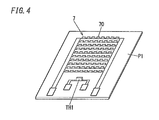
- the thermistor TH1 be placed on the substrate P1 on which the LED 70 is mounted and be in a vicinity of the LED 70 as shown in FIG. 4 .
- the light source 7 includes the substrate P1 on which the solid state light emitting device (LED 70) is mounted, and the temperature detection circuit 5 is mounted on the substrate P1.
- the temperature detection circuit 5 is placed on the substrate P1 on which the LED 70 is mounted as described above, thereby reducing a difference between an actual temperature of the LED 70 and the detection temperature. Note that, it is not always necessary that all of circuit components of the temperature detection circuit 5 are mounted on the substrate P1. In brief, it is sufficient that components of the temperature detection circuit 5 which are necessary for measuring the surrounding temperature are mounted on the substrate P1.
- the control circuit 6 is constituted by a microcomputer, for example.
- the control circuit 6 is configured to control the output (i.e., the operation power) from the power supply circuit 4.
- the control circuit 6 is configured to determine the load current based on the signal voltage of the first detection signal, and to detect zero-crossing of the load current based on the signal voltage of the second detection signal. Further, the control circuit 6 preliminarily stores an intended value of the load current (hereinafter referred to as "intended value of current”), and is configured to change the intended value of current based on the signal voltage of the temperature signal.
- intended value of current an intended value of the load current
- the control circuit 6 is configured to turn on and off the switching device Q2 by providing the control signal thereto. When the signal voltage of the first detection signal reaches the intended value of current, the switching device Q2 is turned off. When the signal voltage of the second detection signal indicates the zero-crossing, the switching device Q2 is turned on. In brief, the control circuit 6 is configured to control the load current in a critical mode as shown in FIG. 5 .
- control circuit 6 is configured to determine a forward voltage of the LED 70 based on a difference between a signal voltage of the third detection signal from the first voltage dividing circuit 40 and a signal voltage of the fourth detection signal from the second voltage dividing circuit 41. When the above difference is small, the control circuit 6 determines that the light source 7 is disconnected. When the above difference is zero, the control circuit 6 determines that the light source 7 is electrically shorted. The control circuit 6 is configured to, when determining that the light source 7 is disconnected or electrically shorted, turn off the switching device Q2 to terminate the operation of the power supply circuit 4.
- control circuit 6 is not limited to a circuit constituted by a microcomputer only.
- the control circuit 6 may be a circuit constituted by a combination of a microcomputer and an IC for power control such as FA5601 available from Fuji Electric and L6562A available from ST Microelectronics. Further, the control circuit 6 may be constituted by a combination of the IC for power control and an analog circuit.
- the light source 7 is constituted by connecting the LEDs 70 in a series-parallel manner.
- the LEDs 70 are solid state light emitting devices. Each LED 70 emits light when a load current flows therethrough in response to the output from the power supply circuit 4. Note that, the light source 7 is not limited to a series circuit of the LEDs 70 but may be a parallel circuit of the LEDs 70 or a series-parallel circuit of the LEDs 70.
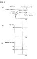
- a device for temperature measurement such as a thermistor is placed in a vicinity of a light source, and the temperature control is performed when a detection temperature exceeds a predetermined threshold. For example, as shown in FIGs. 7 (a) and (b) , when the detection temperature exceeds the threshold, the light source is dimmed such that a percentage of a light output of the light source is decreased from 100 % down to 80 % in order to decrease a temperature of the light source.
- a percentage of the number of revolutions of the fan to a normal number of revolutions is increased from 100 % up to 150 % as shown in FIG. 7 (c) in order to decrease the temperature of the light source.
- the detection temperature is compared with the predetermined threshold and the temperature control is performed such that the temperature of the LED constituting the light source does not exceed an allowable temperature of the LED.
- a correlation between an actual temperature of the LED and the detection temperature is affected by some causes such as a power loss in the LED, a positional relation between the LED and a device for temperature measurement, and installation conditions of the LED and the device for temperature measurement. Further, when the LED is thermally connected to a heat sink, the above correlation is also affected by a size of the heat sink and a connection condition between the LED and the heat sink. Additionally, when a fan is used for cooling the light source, a performance of the fan also affects the above correlation.
- the above correlation may be lost due to the deterioration in the heat dissipation performance of the heat sink.
- the LED and the heat sink are connected incompletely due to aging deterioration, the above correlation may be lost due to the deterioration in the heat dissipation performance of the heat sink.
- the fan is used for cooling the light source, the heat dissipation performance of the fan becomes poor due to a deterioration of the fan and thereby the above correlation may be lost.
- the power supply circuit which supplies power to the light source operates abnormally to overload the LED, the LED may be excessively heated and thus the above correlation may be lost.
- the detection temperature does not exceed the threshold and accordingly the temperature control is not performed. Nevertheless, the actual temperature of the LED exceeds the allowable temperature. Further, in a case shown in FIG. 9 , the detection temperature exceeds the threshold and accordingly the temperature control is performed. Nevertheless, the actual temperature of the LED exceeds the allowable temperature.
- the lighting device of the present embodiment performs the temperature control as follows.
- each circuit when power supply to the lighting device of the present embodiment starts, each circuit operates to turn on the LED 70 and therefore the temperature of the LED 70 starts to increase.
- the signal voltage of the temperature signal also increases with an increase in the temperature of the LED 70.
- the control circuit 6 measures required time T1 necessary for the signal voltage of the temperature signal to reach a second threshold after the signal voltage of the temperature signal reaches a first threshold.
- the second threshold is greater than the first threshold.
- the control circuit 6 determines that the detection temperature operates abnormally, and decreases the intended value of the load current.
- a duty cycle of the switching device Q2 is decreased and therefore the load current flowing through the LED 70 is reduced. Consequently, the light output of the LED 70 decreases.
- the temperature of the LED 70 is decreased with a decrease in the light output of the LED 70.
- the lighting device of the present embodiment includes a temperature control circuit (temperature controlling means) for controlling the temperature of the light source 7.
- the temperature control circuit determines whether the increase rate of the surrounding temperature exceeds the predetermined criterion value. When determining that the increase rate exceeds the criterion value, the temperature control circuit performs a process (temperature decreasing process) of decreasing the temperature of the light source 7. Meanwhile, when determining that the increase rate does not exceed the criterion value, the temperature control circuit does not perform the process (temperature decreasing process).
- the temperature control circuit calculates the required time T1 necessary for the detection temperature to reach the second threshold from the first threshold, when supply of the operation power from the power supply circuit 4 to the light source 7 is started.
- the required time T1 is not greater than the predetermined criterion time T0, the temperature control circuit determines that the increase rate exceeds the criterion value.
- the temperature control circuit is the control circuit 6 for controlling the power supply circuit 4.
- the temperature control circuit is configured to, in the above process (temperature decreasing process), decrease the operation power (i.e., the power supplied from the power supply circuit 4 to the light source 7).
- control circuit 6 serving as the temperature controlling means performs the temperature control on the LED 70 based on not the detection temperature itself but the increase rate of the detection temperature.
- the control circuit 6 can detect the abnormality of the detection temperature in an initial period in which the temperature of the LED 70 rises, as shown in FIG. 3 . Also the control circuit 6 can decrease the percentage of the light output from 100 % down to 50 %, thereby decreasing the temperature of the LED 70.
- the lighting device of the present embodiment can prevent deterioration of the light emission efficiency and the lifetime of the LED 70, for example.
- the degree of decreasing the light output of the light source 7 by the temperature control can be determined based on intended applications.
- control circuit 6 may be configured to, when the signal voltage of the temperature signal reaches a third threshold (greater than the second threshold), decrease the percentage of the light output of the light source 7 from 100 % down to 80 %.
- the temperature of the LED 70 can be adjusted appropriately. Note that, the degree of decreasing the light output of the light source 7 by the temperature control can be determined based on intended applications.
- control circuit 6 may be configured to gradually reduce the light output of the light source 7 with a decrease in the required time T1 (i.e., the control circuit 6 may be configured to change the output from the power supply circuit 4 with an increase or a decrease in the increase rate of the detection temperature).
- the temperature control circuit (control circuit 6), in the process (temperature decreasing process), may determine the operation power according to the magnitude of the increase rate. Particularly, it is preferable that the temperature control circuit (control circuit 6) decrease the operation power as the increase rate increases.
- This configuration can increase the light output of the light source 7 as possible while keeping the temperature of the LED 70 not greater than the allowable temperature. Therefore, it is enabled to avoid that the light output of the light source 7 is decreased more than necessary.
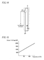
- a set of the thermistor TH1 and the resistor R6 may be replaced with a temperature sensor IC 51 as a thermosensitive device.
- a temperature sensor IC 51 for example, LM50 available from National Semiconductor is used as the temperature sensor IC 51.
- this temperature sensor IC 51 has such a characteristic that a signal voltage of the temperature signal outputted therefrom is proportional to a detection temperature. Therefore, the temperature signal outputted from the temperature sensor IC 51 increases or decreases with an increase or a decrease in the detection temperature in a similar manner to a case in which the set of the thermistor TH1 and the resistor R6 is used.
- control circuit 6 changes the intended value of current based on the signal voltage outputted from the temperature sensor IC 51.
- This configuration can also provide the same advantageous effect as the configuration shown in FIG. 1 .
- a decrease in the temperature of the LED 70 may be achieved by using a cooling device 8 instead of reducing the light output of the light source 7.
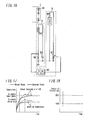
- This configuration includes the cooling device 8 having a fan 80, a drive power source 81, and a drive circuit 82, as shown in FIG. 16 .
- the fan 80 is placed in a vicinity of the light source 7.
- the fan 80 supplies air to the light source 7 to cool the light source 7.
- the fan 80 is a cooler for cooling the light source 7.
- the drive power source 81 is constituted by a microcomputer, for example.
- the drive power source 81 is configured to output a drive voltage for operating the fan 80.
- the fan 80 is a cooler whose cooling capacity increases with an increase in a magnitude of the drive power (in the present embodiment, the drive voltage).
- the drive circuit 82 is configured to vary the number of revolutions of the fan 80 by changing the output voltage from the drive power source 81.
- the drive circuit 82 supplies the drive power (in the present embodiment, the drive voltage) to the cooler (fan 80).
- the drive circuit 82 measures the required time T1 necessary for the signal voltage of the temperature signal from the temperature detection circuit 5 to reach the second threshold after the signal voltage of the temperature signal reaches the first threshold.
- the drive circuit 82 determines that there is no abnormality in the detection temperature. In this case, the drive circuit 82 does not change the output voltage from the drive power source 81.
- the drive circuit 82 determines that the abnormality of the detection temperature occurs, and increases the output voltage from the drive power source 81. Accordingly, the number of revolutions of the fan 80 is increased and therefore the force of the air is also increased. Thus, a cooling effect of the fan 80 increases, and therefore the temperature of the LED 70 is decreased. Consequently, as shown in FIG. 17 , an increase in the temperature of the LED 70 can be suppressed to avoid that the temperature of the LED 70 exceeds the allowable temperature. Thus, the temperature of the LED 70 can be adjusted appropriately.
- the drive circuit 82 changes a percentage of the number of revolutions of the fan 80 from 100 % to 200 % when detecting occurrence of the abnormality of the detection temperature at the initial stage of an increase in the temperature of the LED 70. Therefore, this configuration also can provide the same advantageous effect as the configuration shown in FIG. 1 .
- the temperature control circuit is the drive circuit 82 for adjusting the drive power supplied to the cooler (fan 80).
- the temperature control circuit is configured to, in the process (temperature decreasing process), decrease the drive power (i.e., the power supplied from the drive power source 81 to the fan 80).
- the drive circuit 82 may be configured to increase the number of revolutions of the fan 80 as the required time T1 becomes shorter than the criterion time T0 (i.e., the drive circuit 82 may be configured to change the output from the cooler with an increase or a decrease in the increase rate of the detection temperature).
- the temperature control circuit (drive circuit 82) may determine the drive power according to the magnitude of the increase rate in the process (temperature decreasing process). Particularly, it is preferable that the temperature control circuit (drive circuit 82) increase the drive power as the increase rate increases.
- an optimal temperature control can be performed depending on the abnormality of the LED 70.
- the cooling effect is enhanced as the increase rate of the detection temperature increases.
- the fan 80 is not necessarily required to operate. In brief, the fan 80 may be activated only in the temperature decreasing process.
- the lighting device of the present embodiment may be configured to dim the light source 7 based on a dimming signal received from a dimmer (not shown).
- the power supply circuit 4 may regulate a magnitude of the operation power to a desired value to turn on the light source 7.
- the desired value is determined based on the dimming signal, for example.
- the control circuit 6 can dim the light source 7 by changing the intended value of current (i.e., the output voltage from the power supply circuit 4) based on the dimming signal.
- required time T10 is longer than the required time T1.
- the required time T10 means the required time in the case that the light source 7 is dimmed.
- the required time T1 means the required time in the case that the light source 7 is operated at full power.
- the required time is time necessary for the signal voltage of the temperature signal to reach the second threshold after reaching the first threshold.
- the required time T10 is longer than the required time T1 in some cases. Hence, the required time T10 is likely to not fall below the criterion time T0. In this case, the temperature control on the LED 70 by the control circuit 6 is not performed and therefore the temperature of the LED 70 exceeds the allowable temperature. Consequently, undesirable effects such as decreases in the light emission efficiency and in the lifetime of the LED 70 are likely to occur.
- the control circuit 6 increase or decrease the criterion time T0 depending on the output voltage (desired value) of the power supply circuit 4.
- the temperature control circuit may determine the criterion value according to the desired value. Particularly, it is preferable that the temperature control circuit decrease the criterion value as the desired value decreases.
- the control circuit 6 is configured to increase or decrease the criterion time T0 (i.e., the criterion value) according to an increase or a decrease in the dimming ratio (i.e., an increase or a decrease in the output from the power supply circuit 4).
- the temperature control circuit determines the criterion time T0 according to the desired value. Particularly, it is preferable that the temperature control circuit increase the criterion time T0 as the desired value decreases.
- the control circuit 6 may be configured to keep the first threshold constant and vary the second threshold with a variation in an increase or a decrease in the dimming ratio (an increase or a decrease in the output from the power supply circuit 4).
- the temperature control circuit may determine the second threshold according to the desired value. Particularly, it is preferable that the temperature control circuit decrease the second threshold as the desired value decreases.
- the second threshold is changed with a change in the increase rate of the detection temperature.
- the required time T1 is not changed with a change in the dimming ratio.
- the control circuit 6 determines that the abnormality of the detection temperature occurs. The control circuit 6 then reduces the intended value of the load current to decrease the light output of the light source 7.
- this configuration also can perform the temperature control on the LED 70 in a case where the light source 7 is dimmed.
- control circuit 6 may be configured to keep the second threshold constant and vary the first threshold with a variation in the dimming ratio.
- the temperature control circuit may determine the first threshold according to the desired value. Particularly, it is preferable that the temperature control circuit increase the first threshold as the desired value decreases. This configuration can produce the same advantageous effect as the above.
- the temperature control circuit determines a difference between the first threshold and the second threshold. Especially, it is preferable that the temperature control circuit decrease the difference between the first threshold and the second threshold as the desired value decreases. In other words, it is preferred that the temperature control circuit (control circuit 6) changes a formula for calculating the increase rate (formula for calculating the required time T1) to prevent the increase rate from changing with a change in the desired value.
- the light source 7 can be dimmed by an intermittent control.
- an operation period and a rest period are repeated alternately.
- the switching device Q2 is turned on and off alternately, and in the rest period the switching device Q2 is kept turned off.
- the temperature of the LED 70 increases gradually. Accordingly, in a similar manner as the above, the criterion time T0 or the second threshold may be varied with a variation in the dimming ratio (an increase or a decrease in the output from the power supply circuit 4).
- the control circuit 6 decreases the light output of the light source 7 when the required time T1 falls below the criterion time T0, as shown in FIG. 27 . Therefore, this configuration also makes it possible to perform the temperature control on the LED 70 in a case that the light source 7 is dimmed.
- the above explanation is made to a case that the control circuit 6 serves as the temperature controlling means.
- the above technical concept can be applied to a case that the drive circuit 82 serves as the temperature controlling means.
- the drive circuit 82 may vary the criterion time T0 or the second threshold with a variation in the dimming ratio.
- the LED 70 is used as a solid state light emitting device used for the light source 7.
- the light source 7 may be constituted by another solid state light emitting device such as a semiconductor laser device and an organic EL device.
- the lighting device of the present embodiment includes: the power supply circuit 4 configured to supply power to the light source 7 with the solid state light emitting device (LED 70); the temperature detection circuit 5 configured to measure the surrounding temperature of the solid state light emitting device; and the temperature controlling means configured to control the temperature of the solid state light emitting device.
- the temperature controlling means is configured to calculate the increase rate of the detection temperature measured by the temperature detection circuit 5, and decrease the temperature of the solid state light emitting device when the increase rate exceeds the predetermined criterion value.
- the temperature detection circuit 5 be placed on the substrate P1 on which the solid state light emitting device is mounted.
- the temperature controlling means be the control circuit 6 configured to control the output of the power supply circuit 4. Further it is preferable that the control circuit 6 be configured to decrease the temperature of the solid state light emitting device by reducing the output of the power supply circuit 4.
- control circuit 6 be configured to change the output of the power supply circuit 4 depending on an increase and a decrease in the increase rate of the detection temperature.
- the lighting device include the cooling device 8 including the cooler (fan 80) configured to cool the light source 7 and the drive circuit 82 configured to change an output of the cooler (fan 80). Further it is preferable that the temperature controlling means be the drive circuit 82 and that the drive circuit 82 be configured to decrease the temperature of the solid state light emitting device by increasing the output of the cooler (fan 80).
- the drive circuit 82 be configured to change the output of the cooling device 8 depending on an increase and a decrease in the increase rate of the detection temperature.
- the temperature controlling means be configured to change the criterion value depending on an increase and a decrease in the output of the power supply circuit 4.
- the temperature detection circuit 5 be configured to measure the temperature of the solid state light emitting device by use of the thermosensitive device with the characteristics value varying with a change in the temperature thereof.
- the lighting device of the present embodiment includes the following first feature.
- the lighting device includes the power supply circuit 4, the temperature detection circuit 5, and the temperature control circuit (the control circuit 6 or the drive circuit 82).
- the power supply circuit 4 is configured to supply the operation power to the light source 7 including the solid state light emitting device (e.g., the LED 70).
- the temperature detection circuit 5 is configured to measure the surrounding temperature of the light source 7 and output the measured surrounding temperature as the detection temperature.
- the temperature control circuit is configured to determine whether the increase rate of the surrounding temperature exceeds the predetermined criterion value.
- the temperature control circuit is configured to, when determining that the increase rate exceeds the criterion value, perform the process (temperature decreasing process) of decreasing the temperature of the light source 7.
- the lighting device of the present embodiment includes the following second to fourth features. Besides, the second to fourth features are optional.
- the temperature control circuit is the control circuit 6 configured to control the power supply circuit 4.
- the temperature control circuit is configured to, in the process (temperature decreasing process), decrease the operation power.
- the temperature control circuit is configured to, in the process (temperature decreasing process), determine the operation power according to the magnitude of the increase rate.
- the temperature control circuit is configured to, in the process (temperature decreasing process), decrease the operation power as the increase rate increases.
- the lighting device of the present embodiment may include the following fifth to seventh features instead of the second to fourth features.
- the fifth to seventh features are optional.
- the lighting device further includes the cooler (e.g., the fan 80) configured to cool the light source 7.
- the temperature control circuit is the drive circuit 82 configured to control the drive power supplied to the cooler (fan 80).
- the cooler (fan 80) has the cooling capacity increasing with an increase in the magnitude of the drive power.
- the temperature control circuit is configured to, in the process (temperature decreasing process), increase the drive power.
- the temperature control circuit is configured to, in the process (temperature decreasing process), determine the drive power according to the magnitude of the increase rate.
- the temperature control circuit is configured to, in the process (temperature decreasing process), increase the drive power as the increase rate increases.
- the lighting device of the present embodiment includes the following eighth and ninth features. Besides, the eighth and ninth features are optional.
- the power supply circuit 4 is configured to regulate the magnitude of the operation power to the desired value to turn on the light source 7.
- the temperature control circuit is configured to determine the criterion value according to the desired value.
- the temperature control circuit is configured to decrease the criterion value as the desired value decreases.
- the lighting device of the present embodiment includes the following tenth to twelfth features. Besides, the tenth to twelfth features are optional.
- the temperature control circuit is configured to calculate the required time T1 necessary for the detection temperature to reach the second threshold from the first threshold when supply of the operation power from the power supply circuit 4 to the light source 7 is started.
- the temperature control circuit is configured to determine that the increase rate exceeds the criterion value when the required time T1 is not greater than the predetermined criterion time T0.
- the power supply circuit 4 is configured to regulate the magnitude of the operation power to the desired value to turn on the light source 7.
- the temperature control circuit is configured to increase the criterion time T0 as the desired value decreases.
- the power supply circuit 4 is configured to regulate the magnitude of the operation power to the desired value to turn on the light source 7.
- the temperature control circuit is configured to decrease the difference between the first threshold and the second threshold as the desired value decreases.
- the lighting device of the present embodiment includes the following thirteenth and fourteenth features. Besides, the thirteenth and fourteenth features are optional.
- the light source 7 includes the substrate P1 on which the solid state light emitting device is mounted.
- the temperature detection circuit 5 is mounted on the substrate P1.
- the temperature control circuit 5 is configured to measure the surrounding temperature by use of a thermosensitive device having a characteristic value varying with a temperature thereof.
- the temperature controlling means performs the temperature control on the solid state light emitting device based on the increase rate of the detection temperature.
- the temperature controlling means can detect the abnormality of the detection temperature at the initial stage in an increase in the temperature of the solid state light emitting device, and then decrease the temperature of the solid state light emitting device. Consequently, the lighting device of the present embodiment can suppress an increase in the temperature of the solid state light emitting device to avoid that the temperature of the solid state light emitting device exceeds the allowable temperature.
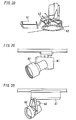
- the lighting device of the present embodiment is available for lighting fixtures shown in FIGs. 28 to 30 , for example.
- Each of the lighting fixtures illustrated in FIGs. 28 to 30 includes a lighting device A1 of the present embodiment and a fixture body A2 configured to hold the light source 7.
- each lighting fixture includes the fixture body A2 configured to hold the light source 7 and the lighting device A1 for operating the light source 7.
- the lighting device A1 has the aforementioned first feature. Note that, the lighting device A1 may have at least one of the aforementioned second to fourteenth features, if needed.
- the lighting fixture shown in FIG. 28 is a down light
- the lighting fixtures shown in FIGs. 29 and 30 are spot lights.
- the lighting device A1 is connected to the light source 7 through a cable A3.
- the aforementioned lighting fixture includes the lighting device A1 and therefore can produce the same effect as the lighting device A1 of the present embodiment.
- the lighting fixture described above may be used alone but a plurality of lighting fixtures described above may be used to constitute a lighting system.
Landscapes
- Circuit Arrangement For Electric Light Sources In General (AREA)
- Circuit Arrangements For Discharge Lamps (AREA)
Applications Claiming Priority (1)
| Application Number | Priority Date | Filing Date | Title |
|---|---|---|---|
| JP2013029200A JP2014157781A (ja) | 2013-02-18 | 2013-02-18 | 点灯装置及びそれを用いた照明器具 |
Publications (3)
| Publication Number | Publication Date |
|---|---|
| EP2768286A2 true EP2768286A2 (fr) | 2014-08-20 |
| EP2768286A3 EP2768286A3 (fr) | 2016-02-24 |
| EP2768286B1 EP2768286B1 (fr) | 2018-01-17 |
Family
ID=50112797
Family Applications (1)
| Application Number | Title | Priority Date | Filing Date |
|---|---|---|---|
| EP14155361.0A Not-in-force EP2768286B1 (fr) | 2013-02-18 | 2014-02-17 | Dispositif d'éclairage et accessoire d'éclairage |
Country Status (4)
| Country | Link |
|---|---|
| US (1) | US9392668B2 (fr) |
| EP (1) | EP2768286B1 (fr) |
| JP (1) | JP2014157781A (fr) |
| CN (1) | CN103997811B (fr) |
Cited By (1)
| Publication number | Priority date | Publication date | Assignee | Title |
|---|---|---|---|---|
| WO2017067822A1 (fr) * | 2015-10-20 | 2017-04-27 | Technische Universität Darmstadt | Procédé de commande d'un dispositif d'éclairage et dispositif d'éclairage |
Families Citing this family (14)
| Publication number | Priority date | Publication date | Assignee | Title |
|---|---|---|---|---|
| JP6153024B2 (ja) * | 2013-07-26 | 2017-06-28 | パナソニックIpマネジメント株式会社 | 発光素子点灯装置、発光モジュール、照明装置及び発光素子の点灯方法 |
| DE102015214090B4 (de) * | 2015-07-24 | 2026-03-26 | Osram Gmbh | Beleuchtungseinrichtung |
| JP6566354B2 (ja) * | 2015-08-25 | 2019-08-28 | パナソニックIpマネジメント株式会社 | 調光制御装置、照明システム、及び設備機器 |
| CN105577003B (zh) * | 2016-01-21 | 2017-12-29 | 广州金升阳科技有限公司 | 一种带有源功率因数校正的开关电源 |
| JP6799807B2 (ja) * | 2016-08-30 | 2020-12-16 | パナソニックIpマネジメント株式会社 | 点灯装置、照明器具、及びそれを備える車両 |
| US10237940B2 (en) * | 2016-12-23 | 2019-03-19 | Infineon Technologies Ag | Thermal protection for light emitting devices |
| TWI666969B (zh) * | 2017-01-06 | 2019-07-21 | 日商東芝照明技術股份有限公司 | 電源裝置以及具備此電源裝置的照明裝置 |
| CN106793336B (zh) * | 2017-01-20 | 2018-11-09 | 陕西亚成微电子股份有限公司 | 一种led驱动电路及其驱动方法 |
| DE102018201228A1 (de) * | 2017-07-24 | 2019-01-24 | Osram Gmbh | Steuern von wenigstens zwei in reihe geschalteten leuchtdioden einer leuchteinrichtung |
| US10779366B2 (en) * | 2018-09-25 | 2020-09-15 | Panasonic Intellectual Property Management Co., Ltd. | Lighting apparatus, luminaire, movable object, control method, and non-transitory recording medium |
| JP7558646B2 (ja) * | 2019-04-19 | 2024-10-01 | 三菱電機株式会社 | 照明器具および温度検知ユニット |
| US11931472B1 (en) | 2020-12-18 | 2024-03-19 | Zoox, Inc. | Vehicle with UVC light emitters |
| US11730844B1 (en) * | 2020-12-18 | 2023-08-22 | Zoox, Inc. | Method of disinfecting vehicle using UVC light emitters |
| JP2022167486A (ja) * | 2021-04-23 | 2022-11-04 | トヨタ自動車株式会社 | 車両運用システム及び自動運転車両 |
Citations (1)
| Publication number | Priority date | Publication date | Assignee | Title |
|---|---|---|---|---|
| JP2010272472A (ja) | 2009-05-25 | 2010-12-02 | Stanley Electric Co Ltd | Led照明装置 |
Family Cites Families (14)
| Publication number | Priority date | Publication date | Assignee | Title |
|---|---|---|---|---|
| JPH10312888A (ja) | 1997-05-14 | 1998-11-24 | Toshiba Corp | ランプ点灯装置 |
| US7262752B2 (en) * | 2001-01-16 | 2007-08-28 | Visteon Global Technologies, Inc. | Series led backlight control circuit |
| JP4299006B2 (ja) | 2003-01-08 | 2009-07-22 | パナソニック株式会社 | 携帯型led照明装置 |
| JP2004345319A (ja) * | 2003-05-26 | 2004-12-09 | Konica Minolta Business Technologies Inc | 画像記録装置 |
| JP4152348B2 (ja) * | 2004-06-03 | 2008-09-17 | 株式会社ソニー・コンピュータエンタテインメント | 電子デバイス冷却装置、電子デバイスシステムおよび電子デバイス冷却方法 |
| JP4734900B2 (ja) | 2004-11-19 | 2011-07-27 | ソニー株式会社 | バックライト装置 |
| WO2006092040A1 (fr) * | 2005-03-03 | 2006-09-08 | Tir Systems Ltd. | Procede et appareil de commande de contrainte thermique dans des dispositifs electroluminescents |
| JP4762044B2 (ja) * | 2006-04-27 | 2011-08-31 | 矢崎総業株式会社 | 負荷回路の保護装置 |
| JP2010192406A (ja) | 2009-02-20 | 2010-09-02 | Toshiba Lighting & Technology Corp | Led点灯装置 |
| CN101795516A (zh) * | 2010-01-27 | 2010-08-04 | 裘伟光 | 一种高能led照明热效应预警和检测的方法 |
| JP5590987B2 (ja) | 2010-06-23 | 2014-09-17 | 三菱電機株式会社 | 誘導加熱調理器 |
| JP5955502B2 (ja) * | 2010-12-09 | 2016-07-20 | 矢崎総業株式会社 | 負荷回路の断線検出装置 |
| JP5549583B2 (ja) * | 2010-12-27 | 2014-07-16 | 株式会社デンソー | 点灯装置および灯具 |
| CN102869155A (zh) * | 2012-09-06 | 2013-01-09 | 上海晶丰明源半导体有限公司 | 一种发光二极管驱动电源控制电路及其控制方法 |
-
2013
- 2013-02-18 JP JP2013029200A patent/JP2014157781A/ja active Pending
-
2014
- 2014-02-14 US US14/180,502 patent/US9392668B2/en not_active Expired - Fee Related
- 2014-02-17 EP EP14155361.0A patent/EP2768286B1/fr not_active Not-in-force
- 2014-02-18 CN CN201410054823.2A patent/CN103997811B/zh not_active Expired - Fee Related
Patent Citations (1)
| Publication number | Priority date | Publication date | Assignee | Title |
|---|---|---|---|---|
| JP2010272472A (ja) | 2009-05-25 | 2010-12-02 | Stanley Electric Co Ltd | Led照明装置 |
Cited By (1)
| Publication number | Priority date | Publication date | Assignee | Title |
|---|---|---|---|---|
| WO2017067822A1 (fr) * | 2015-10-20 | 2017-04-27 | Technische Universität Darmstadt | Procédé de commande d'un dispositif d'éclairage et dispositif d'éclairage |
Also Published As
| Publication number | Publication date |
|---|---|
| JP2014157781A (ja) | 2014-08-28 |
| US9392668B2 (en) | 2016-07-12 |
| CN103997811A (zh) | 2014-08-20 |
| EP2768286B1 (fr) | 2018-01-17 |
| US20140232268A1 (en) | 2014-08-21 |
| EP2768286A3 (fr) | 2016-02-24 |
| CN103997811B (zh) | 2017-06-23 |
Similar Documents
| Publication | Publication Date | Title |
|---|---|---|
| EP2768286B1 (fr) | Dispositif d'éclairage et accessoire d'éclairage | |
| US9560711B2 (en) | Method and device for remote sensing and control of LED lights | |
| EP2768281B1 (fr) | Dispositif d'éclairage et accessoire d'éclairage | |
| US9763295B2 (en) | Switching converter and lighting device using the same | |
| CN102316627B (zh) | Led点灯装置 | |
| EP3259961B1 (fr) | Dispositif et procédé de commande de limitation de repli thermique de diode électroluminescente | |
| US9113509B2 (en) | Lighting device and lighting fixture | |
| US9018860B2 (en) | LED lighting device | |
| CN102695326A (zh) | 具有保护功能的控制器及发光二极管驱动电路 | |
| JP5959548B2 (ja) | 発光ダイオード表示装置及びその制御方法 | |
| KR20140104196A (ko) | Led 조명기구 전원 공급회로 | |
| CN108112135B (zh) | Led灯具及其电源电路 | |
| JP2014157782A (ja) | 点灯装置及びそれを用いた照明器具 | |
| JP2019192375A (ja) | 光源用電源装置、照明装置及び照明システム | |
| CN113498232A (zh) | 具有对驱动器的热保护的照明设备 | |
| JP6017818B2 (ja) | 点灯装置及び照明装置 | |
| KR20140019888A (ko) | 발광 다이오드 조명 장치 | |
| JP2014135241A (ja) | 照明装置 | |
| KR20160106962A (ko) | Led 전원공급회로 |
Legal Events
| Date | Code | Title | Description |
|---|---|---|---|
| PUAI | Public reference made under article 153(3) epc to a published international application that has entered the european phase |
Free format text: ORIGINAL CODE: 0009012 |
|
| 17P | Request for examination filed |
Effective date: 20140217 |
|
| AK | Designated contracting states |
Kind code of ref document: A2 Designated state(s): AL AT BE BG CH CY CZ DE DK EE ES FI FR GB GR HR HU IE IS IT LI LT LU LV MC MK MT NL NO PL PT RO RS SE SI SK SM TR |
|
| AX | Request for extension of the european patent |
Extension state: BA ME |
|
| RAP1 | Party data changed (applicant data changed or rights of an application transferred) |
Owner name: PANASONIC INTELLECTUAL PROPERTY MANAGEMENT CO., LT |
|
| PUAL | Search report despatched |
Free format text: ORIGINAL CODE: 0009013 |
|
| AK | Designated contracting states |
Kind code of ref document: A3 Designated state(s): AL AT BE BG CH CY CZ DE DK EE ES FI FR GB GR HR HU IE IS IT LI LT LU LV MC MK MT NL NO PL PT RO RS SE SI SK SM TR |
|
| AX | Request for extension of the european patent |
Extension state: BA ME |
|
| RIC1 | Information provided on ipc code assigned before grant |
Ipc: H05B 33/08 20060101ALI20160119BHEP Ipc: H05B 37/00 20060101AFI20160119BHEP |
|
| 17Q | First examination report despatched |
Effective date: 20160801 |
|
| STAA | Information on the status of an ep patent application or granted ep patent |
Free format text: STATUS: EXAMINATION IS IN PROGRESS |
|
| GRAP | Despatch of communication of intention to grant a patent |
Free format text: ORIGINAL CODE: EPIDOSNIGR1 |
|
| STAA | Information on the status of an ep patent application or granted ep patent |
Free format text: STATUS: GRANT OF PATENT IS INTENDED |
|
| INTG | Intention to grant announced |
Effective date: 20170918 |
|
| GRAS | Grant fee paid |
Free format text: ORIGINAL CODE: EPIDOSNIGR3 |
|
| GRAA | (expected) grant |
Free format text: ORIGINAL CODE: 0009210 |
|
| STAA | Information on the status of an ep patent application or granted ep patent |
Free format text: STATUS: THE PATENT HAS BEEN GRANTED |
|
| AK | Designated contracting states |
Kind code of ref document: B1 Designated state(s): AL AT BE BG CH CY CZ DE DK EE ES FI FR GB GR HR HU IE IS IT LI LT LU LV MC MK MT NL NO PL PT RO RS SE SI SK SM TR |
|
| REG | Reference to a national code |
Ref country code: GB Ref legal event code: FG4D |
|
| REG | Reference to a national code |
Ref country code: CH Ref legal event code: EP |
|
| REG | Reference to a national code |
Ref country code: IE Ref legal event code: FG4D |
|
| REG | Reference to a national code |
Ref country code: AT Ref legal event code: REF Ref document number: 965230 Country of ref document: AT Kind code of ref document: T Effective date: 20180215 |
|
| REG | Reference to a national code |
Ref country code: DE Ref legal event code: R096 Ref document number: 602014019962 Country of ref document: DE |
|
| REG | Reference to a national code |
Ref country code: NL Ref legal event code: MP Effective date: 20180117 |
|
| REG | Reference to a national code |
Ref country code: LT Ref legal event code: MG4D |
|
| REG | Reference to a national code |
Ref country code: AT Ref legal event code: MK05 Ref document number: 965230 Country of ref document: AT Kind code of ref document: T Effective date: 20180117 |
|
| PG25 | Lapsed in a contracting state [announced via postgrant information from national office to epo] |
Ref country code: NL Free format text: LAPSE BECAUSE OF FAILURE TO SUBMIT A TRANSLATION OF THE DESCRIPTION OR TO PAY THE FEE WITHIN THE PRESCRIBED TIME-LIMIT Effective date: 20180117 |
|
| PG25 | Lapsed in a contracting state [announced via postgrant information from national office to epo] |
Ref country code: HR Free format text: LAPSE BECAUSE OF FAILURE TO SUBMIT A TRANSLATION OF THE DESCRIPTION OR TO PAY THE FEE WITHIN THE PRESCRIBED TIME-LIMIT Effective date: 20180117 Ref country code: LT Free format text: LAPSE BECAUSE OF FAILURE TO SUBMIT A TRANSLATION OF THE DESCRIPTION OR TO PAY THE FEE WITHIN THE PRESCRIBED TIME-LIMIT Effective date: 20180117 Ref country code: CY Free format text: LAPSE BECAUSE OF FAILURE TO SUBMIT A TRANSLATION OF THE DESCRIPTION OR TO PAY THE FEE WITHIN THE PRESCRIBED TIME-LIMIT Effective date: 20180117 Ref country code: NO Free format text: LAPSE BECAUSE OF FAILURE TO SUBMIT A TRANSLATION OF THE DESCRIPTION OR TO PAY THE FEE WITHIN THE PRESCRIBED TIME-LIMIT Effective date: 20180417 Ref country code: ES Free format text: LAPSE BECAUSE OF FAILURE TO SUBMIT A TRANSLATION OF THE DESCRIPTION OR TO PAY THE FEE WITHIN THE PRESCRIBED TIME-LIMIT Effective date: 20180117 Ref country code: FI Free format text: LAPSE BECAUSE OF FAILURE TO SUBMIT A TRANSLATION OF THE DESCRIPTION OR TO PAY THE FEE WITHIN THE PRESCRIBED TIME-LIMIT Effective date: 20180117 |
|
| PG25 | Lapsed in a contracting state [announced via postgrant information from national office to epo] |
Ref country code: LV Free format text: LAPSE BECAUSE OF FAILURE TO SUBMIT A TRANSLATION OF THE DESCRIPTION OR TO PAY THE FEE WITHIN THE PRESCRIBED TIME-LIMIT Effective date: 20180117 Ref country code: SE Free format text: LAPSE BECAUSE OF FAILURE TO SUBMIT A TRANSLATION OF THE DESCRIPTION OR TO PAY THE FEE WITHIN THE PRESCRIBED TIME-LIMIT Effective date: 20180117 Ref country code: GR Free format text: LAPSE BECAUSE OF FAILURE TO SUBMIT A TRANSLATION OF THE DESCRIPTION OR TO PAY THE FEE WITHIN THE PRESCRIBED TIME-LIMIT Effective date: 20180418 Ref country code: PL Free format text: LAPSE BECAUSE OF FAILURE TO SUBMIT A TRANSLATION OF THE DESCRIPTION OR TO PAY THE FEE WITHIN THE PRESCRIBED TIME-LIMIT Effective date: 20180117 Ref country code: BG Free format text: LAPSE BECAUSE OF FAILURE TO SUBMIT A TRANSLATION OF THE DESCRIPTION OR TO PAY THE FEE WITHIN THE PRESCRIBED TIME-LIMIT Effective date: 20180417 Ref country code: IS Free format text: LAPSE BECAUSE OF FAILURE TO SUBMIT A TRANSLATION OF THE DESCRIPTION OR TO PAY THE FEE WITHIN THE PRESCRIBED TIME-LIMIT Effective date: 20180517 Ref country code: RS Free format text: LAPSE BECAUSE OF FAILURE TO SUBMIT A TRANSLATION OF THE DESCRIPTION OR TO PAY THE FEE WITHIN THE PRESCRIBED TIME-LIMIT Effective date: 20180117 Ref country code: AT Free format text: LAPSE BECAUSE OF FAILURE TO SUBMIT A TRANSLATION OF THE DESCRIPTION OR TO PAY THE FEE WITHIN THE PRESCRIBED TIME-LIMIT Effective date: 20180117 |
|
| REG | Reference to a national code |
Ref country code: CH Ref legal event code: PL |
|
| REG | Reference to a national code |
Ref country code: DE Ref legal event code: R097 Ref document number: 602014019962 Country of ref document: DE |
|
| PG25 | Lapsed in a contracting state [announced via postgrant information from national office to epo] |
Ref country code: IT Free format text: LAPSE BECAUSE OF FAILURE TO SUBMIT A TRANSLATION OF THE DESCRIPTION OR TO PAY THE FEE WITHIN THE PRESCRIBED TIME-LIMIT Effective date: 20180117 Ref country code: MC Free format text: LAPSE BECAUSE OF FAILURE TO SUBMIT A TRANSLATION OF THE DESCRIPTION OR TO PAY THE FEE WITHIN THE PRESCRIBED TIME-LIMIT Effective date: 20180117 Ref country code: AL Free format text: LAPSE BECAUSE OF FAILURE TO SUBMIT A TRANSLATION OF THE DESCRIPTION OR TO PAY THE FEE WITHIN THE PRESCRIBED TIME-LIMIT Effective date: 20180117 Ref country code: EE Free format text: LAPSE BECAUSE OF FAILURE TO SUBMIT A TRANSLATION OF THE DESCRIPTION OR TO PAY THE FEE WITHIN THE PRESCRIBED TIME-LIMIT Effective date: 20180117 Ref country code: RO Free format text: LAPSE BECAUSE OF FAILURE TO SUBMIT A TRANSLATION OF THE DESCRIPTION OR TO PAY THE FEE WITHIN THE PRESCRIBED TIME-LIMIT Effective date: 20180117 |
|
| PLBE | No opposition filed within time limit |
Free format text: ORIGINAL CODE: 0009261 |
|
| STAA | Information on the status of an ep patent application or granted ep patent |
Free format text: STATUS: NO OPPOSITION FILED WITHIN TIME LIMIT |
|
| REG | Reference to a national code |
Ref country code: IE Ref legal event code: MM4A |
|
| REG | Reference to a national code |
Ref country code: BE Ref legal event code: MM Effective date: 20180228 |
|
| PG25 | Lapsed in a contracting state [announced via postgrant information from national office to epo] |
Ref country code: SM Free format text: LAPSE BECAUSE OF FAILURE TO SUBMIT A TRANSLATION OF THE DESCRIPTION OR TO PAY THE FEE WITHIN THE PRESCRIBED TIME-LIMIT Effective date: 20180117 Ref country code: CZ Free format text: LAPSE BECAUSE OF FAILURE TO SUBMIT A TRANSLATION OF THE DESCRIPTION OR TO PAY THE FEE WITHIN THE PRESCRIBED TIME-LIMIT Effective date: 20180117 Ref country code: LU Free format text: LAPSE BECAUSE OF NON-PAYMENT OF DUE FEES Effective date: 20180217 Ref country code: CH Free format text: LAPSE BECAUSE OF NON-PAYMENT OF DUE FEES Effective date: 20180228 Ref country code: DK Free format text: LAPSE BECAUSE OF FAILURE TO SUBMIT A TRANSLATION OF THE DESCRIPTION OR TO PAY THE FEE WITHIN THE PRESCRIBED TIME-LIMIT Effective date: 20180117 Ref country code: SK Free format text: LAPSE BECAUSE OF FAILURE TO SUBMIT A TRANSLATION OF THE DESCRIPTION OR TO PAY THE FEE WITHIN THE PRESCRIBED TIME-LIMIT Effective date: 20180117 Ref country code: LI Free format text: LAPSE BECAUSE OF NON-PAYMENT OF DUE FEES Effective date: 20180228 |
|
| REG | Reference to a national code |
Ref country code: FR Ref legal event code: ST Effective date: 20181031 |
|
| 26N | No opposition filed |
Effective date: 20181018 |
|
| GBPC | Gb: european patent ceased through non-payment of renewal fee |
Effective date: 20180417 |
|
| PG25 | Lapsed in a contracting state [announced via postgrant information from national office to epo] |
Ref country code: IE Free format text: LAPSE BECAUSE OF NON-PAYMENT OF DUE FEES Effective date: 20180217 |
|
| PG25 | Lapsed in a contracting state [announced via postgrant information from national office to epo] |
Ref country code: BE Free format text: LAPSE BECAUSE OF NON-PAYMENT OF DUE FEES Effective date: 20180228 Ref country code: GB Free format text: LAPSE BECAUSE OF NON-PAYMENT OF DUE FEES Effective date: 20180417 Ref country code: FR Free format text: LAPSE BECAUSE OF NON-PAYMENT OF DUE FEES Effective date: 20180319 Ref country code: SI Free format text: LAPSE BECAUSE OF FAILURE TO SUBMIT A TRANSLATION OF THE DESCRIPTION OR TO PAY THE FEE WITHIN THE PRESCRIBED TIME-LIMIT Effective date: 20180117 |
|
| PGFP | Annual fee paid to national office [announced via postgrant information from national office to epo] |
Ref country code: DE Payment date: 20190219 Year of fee payment: 6 |
|
| PG25 | Lapsed in a contracting state [announced via postgrant information from national office to epo] |
Ref country code: MT Free format text: LAPSE BECAUSE OF NON-PAYMENT OF DUE FEES Effective date: 20180217 |
|
| PG25 | Lapsed in a contracting state [announced via postgrant information from national office to epo] |
Ref country code: TR Free format text: LAPSE BECAUSE OF FAILURE TO SUBMIT A TRANSLATION OF THE DESCRIPTION OR TO PAY THE FEE WITHIN THE PRESCRIBED TIME-LIMIT Effective date: 20180117 |
|
| PG25 | Lapsed in a contracting state [announced via postgrant information from national office to epo] |
Ref country code: HU Free format text: LAPSE BECAUSE OF FAILURE TO SUBMIT A TRANSLATION OF THE DESCRIPTION OR TO PAY THE FEE WITHIN THE PRESCRIBED TIME-LIMIT; INVALID AB INITIO Effective date: 20140217 Ref country code: PT Free format text: LAPSE BECAUSE OF FAILURE TO SUBMIT A TRANSLATION OF THE DESCRIPTION OR TO PAY THE FEE WITHIN THE PRESCRIBED TIME-LIMIT Effective date: 20180117 |
|
| PG25 | Lapsed in a contracting state [announced via postgrant information from national office to epo] |
Ref country code: MK Free format text: LAPSE BECAUSE OF NON-PAYMENT OF DUE FEES Effective date: 20180117 |
|
| REG | Reference to a national code |
Ref country code: DE Ref legal event code: R119 Ref document number: 602014019962 Country of ref document: DE |
|
| PG25 | Lapsed in a contracting state [announced via postgrant information from national office to epo] |
Ref country code: DE Free format text: LAPSE BECAUSE OF NON-PAYMENT OF DUE FEES Effective date: 20200901 |