EP2772936B1 - Drahtverbindungsverfahren für Paralleldrähte sowie ein Verfahren zur Umformung derselben, sowie die entsprechende Arbeitsgeräte - Google Patents
Drahtverbindungsverfahren für Paralleldrähte sowie ein Verfahren zur Umformung derselben, sowie die entsprechende Arbeitsgeräte Download PDFInfo
- Publication number
- EP2772936B1 EP2772936B1 EP14157235.4A EP14157235A EP2772936B1 EP 2772936 B1 EP2772936 B1 EP 2772936B1 EP 14157235 A EP14157235 A EP 14157235A EP 2772936 B1 EP2772936 B1 EP 2772936B1
- Authority
- EP
- European Patent Office
- Prior art keywords
- wires
- interconnection
- elements
- length
- interconnected
- Prior art date
- Legal status (The legal status is an assumption and is not a legal conclusion. Google has not performed a legal analysis and makes no representation as to the accuracy of the status listed.)
- Active
Links
Images


Classifications
-
- H—ELECTRICITY
- H10—SEMICONDUCTOR DEVICES; ELECTRIC SOLID-STATE DEVICES NOT OTHERWISE PROVIDED FOR
- H10W—GENERIC PACKAGES, INTERCONNECTIONS, CONNECTORS OR OTHER CONSTRUCTIONAL DETAILS OF DEVICES COVERED BY CLASS H10
- H10W44/00—Electrical arrangements for controlling or matching impedance
- H10W44/20—Electrical arrangements for controlling or matching impedance at high-frequency [HF] or radio frequency [RF]
- H10W44/203—Electrical connections
- H10W44/206—Wires
-
- H—ELECTRICITY
- H10—SEMICONDUCTOR DEVICES; ELECTRIC SOLID-STATE DEVICES NOT OTHERWISE PROVIDED FOR
- H10W—GENERIC PACKAGES, INTERCONNECTIONS, CONNECTORS OR OTHER CONSTRUCTIONAL DETAILS OF DEVICES COVERED BY CLASS H10
- H10W72/00—Interconnections or connectors in packages
- H10W72/01—Manufacture or treatment
- H10W72/015—Manufacture or treatment of bond wires
- H10W72/01515—Forming coatings
-
- H—ELECTRICITY
- H10—SEMICONDUCTOR DEVICES; ELECTRIC SOLID-STATE DEVICES NOT OTHERWISE PROVIDED FOR
- H10W—GENERIC PACKAGES, INTERCONNECTIONS, CONNECTORS OR OTHER CONSTRUCTIONAL DETAILS OF DEVICES COVERED BY CLASS H10
- H10W72/00—Interconnections or connectors in packages
- H10W72/01—Manufacture or treatment
- H10W72/015—Manufacture or treatment of bond wires
- H10W72/01551—Changing the shapes of bond wires
-
- H—ELECTRICITY
- H10—SEMICONDUCTOR DEVICES; ELECTRIC SOLID-STATE DEVICES NOT OTHERWISE PROVIDED FOR
- H10W—GENERIC PACKAGES, INTERCONNECTIONS, CONNECTORS OR OTHER CONSTRUCTIONAL DETAILS OF DEVICES COVERED BY CLASS H10
- H10W72/00—Interconnections or connectors in packages
- H10W72/071—Connecting or disconnecting
- H10W72/0711—Apparatus therefor
- H10W72/07163—Means for mechanical processing, e.g. for planarising, pressing, stamping or drilling
-
- H—ELECTRICITY
- H10—SEMICONDUCTOR DEVICES; ELECTRIC SOLID-STATE DEVICES NOT OTHERWISE PROVIDED FOR
- H10W—GENERIC PACKAGES, INTERCONNECTIONS, CONNECTORS OR OTHER CONSTRUCTIONAL DETAILS OF DEVICES COVERED BY CLASS H10
- H10W72/00—Interconnections or connectors in packages
- H10W72/071—Connecting or disconnecting
- H10W72/075—Connecting or disconnecting of bond wires
- H10W72/07531—Techniques
- H10W72/07532—Compression bonding, e.g. thermocompression bonding
- H10W72/07533—Ultrasonic bonding, e.g. thermosonic bonding
-
- H—ELECTRICITY
- H10—SEMICONDUCTOR DEVICES; ELECTRIC SOLID-STATE DEVICES NOT OTHERWISE PROVIDED FOR
- H10W—GENERIC PACKAGES, INTERCONNECTIONS, CONNECTORS OR OTHER CONSTRUCTIONAL DETAILS OF DEVICES COVERED BY CLASS H10
- H10W72/00—Interconnections or connectors in packages
- H10W72/071—Connecting or disconnecting
- H10W72/075—Connecting or disconnecting of bond wires
- H10W72/07531—Techniques
- H10W72/07536—Soldering or alloying
-
- H—ELECTRICITY
- H10—SEMICONDUCTOR DEVICES; ELECTRIC SOLID-STATE DEVICES NOT OTHERWISE PROVIDED FOR
- H10W—GENERIC PACKAGES, INTERCONNECTIONS, CONNECTORS OR OTHER CONSTRUCTIONAL DETAILS OF DEVICES COVERED BY CLASS H10
- H10W72/00—Interconnections or connectors in packages
- H10W72/071—Connecting or disconnecting
- H10W72/075—Connecting or disconnecting of bond wires
- H10W72/07531—Techniques
- H10W72/07537—Techniques using a polymer adhesive, e.g. an adhesive based on silicone or epoxy
-
- H—ELECTRICITY
- H10—SEMICONDUCTOR DEVICES; ELECTRIC SOLID-STATE DEVICES NOT OTHERWISE PROVIDED FOR
- H10W—GENERIC PACKAGES, INTERCONNECTIONS, CONNECTORS OR OTHER CONSTRUCTIONAL DETAILS OF DEVICES COVERED BY CLASS H10
- H10W72/00—Interconnections or connectors in packages
- H10W72/071—Connecting or disconnecting
- H10W72/075—Connecting or disconnecting of bond wires
- H10W72/07541—Controlling the environment, e.g. atmosphere composition or temperature
- H10W72/07552—Controlling the environment, e.g. atmosphere composition or temperature changes in structures or sizes
-
- H—ELECTRICITY
- H10—SEMICONDUCTOR DEVICES; ELECTRIC SOLID-STATE DEVICES NOT OTHERWISE PROVIDED FOR
- H10W—GENERIC PACKAGES, INTERCONNECTIONS, CONNECTORS OR OTHER CONSTRUCTIONAL DETAILS OF DEVICES COVERED BY CLASS H10
- H10W72/00—Interconnections or connectors in packages
- H10W72/071—Connecting or disconnecting
- H10W72/075—Connecting or disconnecting of bond wires
- H10W72/07541—Controlling the environment, e.g. atmosphere composition or temperature
- H10W72/07553—Controlling the environment, e.g. atmosphere composition or temperature changes in shapes
-
- H—ELECTRICITY
- H10—SEMICONDUCTOR DEVICES; ELECTRIC SOLID-STATE DEVICES NOT OTHERWISE PROVIDED FOR
- H10W—GENERIC PACKAGES, INTERCONNECTIONS, CONNECTORS OR OTHER CONSTRUCTIONAL DETAILS OF DEVICES COVERED BY CLASS H10
- H10W72/00—Interconnections or connectors in packages
- H10W72/071—Connecting or disconnecting
- H10W72/075—Connecting or disconnecting of bond wires
- H10W72/07541—Controlling the environment, e.g. atmosphere composition or temperature
- H10W72/07554—Controlling the environment, e.g. atmosphere composition or temperature changes in dispositions
-
- H—ELECTRICITY
- H10—SEMICONDUCTOR DEVICES; ELECTRIC SOLID-STATE DEVICES NOT OTHERWISE PROVIDED FOR
- H10W—GENERIC PACKAGES, INTERCONNECTIONS, CONNECTORS OR OTHER CONSTRUCTIONAL DETAILS OF DEVICES COVERED BY CLASS H10
- H10W72/00—Interconnections or connectors in packages
- H10W72/50—Bond wires
- H10W72/521—Structures or relative sizes of bond wires
- H10W72/522—Multilayered bond wires, e.g. having a coating concentric around a core
-
- H—ELECTRICITY
- H10—SEMICONDUCTOR DEVICES; ELECTRIC SOLID-STATE DEVICES NOT OTHERWISE PROVIDED FOR
- H10W—GENERIC PACKAGES, INTERCONNECTIONS, CONNECTORS OR OTHER CONSTRUCTIONAL DETAILS OF DEVICES COVERED BY CLASS H10
- H10W72/00—Interconnections or connectors in packages
- H10W72/50—Bond wires
- H10W72/531—Shapes of wire connectors
- H10W72/533—Cross-sectional shape
- H10W72/534—Cross-sectional shape being rectangular
-
- H—ELECTRICITY
- H10—SEMICONDUCTOR DEVICES; ELECTRIC SOLID-STATE DEVICES NOT OTHERWISE PROVIDED FOR
- H10W—GENERIC PACKAGES, INTERCONNECTIONS, CONNECTORS OR OTHER CONSTRUCTIONAL DETAILS OF DEVICES COVERED BY CLASS H10
- H10W72/00—Interconnections or connectors in packages
- H10W72/50—Bond wires
- H10W72/531—Shapes of wire connectors
- H10W72/537—Multiple bond wires having different shapes
-
- H—ELECTRICITY
- H10—SEMICONDUCTOR DEVICES; ELECTRIC SOLID-STATE DEVICES NOT OTHERWISE PROVIDED FOR
- H10W—GENERIC PACKAGES, INTERCONNECTIONS, CONNECTORS OR OTHER CONSTRUCTIONAL DETAILS OF DEVICES COVERED BY CLASS H10
- H10W72/00—Interconnections or connectors in packages
- H10W72/50—Bond wires
- H10W72/541—Dispositions of bond wires
- H10W72/5445—Dispositions of bond wires being orthogonal to a side surface of the chip, e.g. parallel arrangements
-
- H—ELECTRICITY
- H10—SEMICONDUCTOR DEVICES; ELECTRIC SOLID-STATE DEVICES NOT OTHERWISE PROVIDED FOR
- H10W—GENERIC PACKAGES, INTERCONNECTIONS, CONNECTORS OR OTHER CONSTRUCTIONAL DETAILS OF DEVICES COVERED BY CLASS H10
- H10W72/00—Interconnections or connectors in packages
- H10W72/50—Bond wires
- H10W72/581—Auxiliary members, e.g. flow barriers
-
- H—ELECTRICITY
- H10—SEMICONDUCTOR DEVICES; ELECTRIC SOLID-STATE DEVICES NOT OTHERWISE PROVIDED FOR
- H10W—GENERIC PACKAGES, INTERCONNECTIONS, CONNECTORS OR OTHER CONSTRUCTIONAL DETAILS OF DEVICES COVERED BY CLASS H10
- H10W72/00—Interconnections or connectors in packages
- H10W72/90—Bond pads, in general
- H10W72/931—Shapes of bond pads
- H10W72/932—Plan-view shape, i.e. in top view
-
- H—ELECTRICITY
- H10—SEMICONDUCTOR DEVICES; ELECTRIC SOLID-STATE DEVICES NOT OTHERWISE PROVIDED FOR
- H10W—GENERIC PACKAGES, INTERCONNECTIONS, CONNECTORS OR OTHER CONSTRUCTIONAL DETAILS OF DEVICES COVERED BY CLASS H10
- H10W90/00—Package configurations
- H10W90/701—Package configurations characterised by the relative positions of pads or connectors relative to package parts
- H10W90/751—Package configurations characterised by the relative positions of pads or connectors relative to package parts of bond wires
- H10W90/753—Package configurations characterised by the relative positions of pads or connectors relative to package parts of bond wires between laterally-adjacent chips
Definitions
- the present invention relates to an interconnection method for electronic circuits, in particular microwave electronic circuits, by coupled parallel wires.
- a subject of the present invention is also a tool for producing an interconnection by means of the method. It applies in particular to electronic links between different electronic circuits.
- the present invention relates to applications for which electrical connections are required, between different electronic circuits.
- electronic circuit can be in the form of an electronic module, for example a chip, of a micromechanical system, usually designated by the acronym of "MEMS", for the English expression of "Micro-Electro-Mechanical System", of an integrated circuit in a package, of a module of simple printed boards or stacked, of a three-dimensional module, etc.
- MEMS micromechanical system
- connections can electrically connect electronic circuits that are physically homogeneous: for example chips between them, or else physically heterogeneous electronic circuits, when it is a question for example of electrically connecting a chip to an interconnection support with a substrate, a printed card, case, etc.
- the signals considered can be fast digital in character or microwave analog.
- the present invention relates to applications in which the aforementioned electrical connections are intended for the transmission of electrical signals occupying a wide band of frequencies, and / or which are located in high frequencies with regard to the dimensions of the connections to be made. , and / or which have high powers.
- the signals considered can be analog or digital in nature. It is for example considered that high frequencies with regard to the dimensions of the connections to be made, respond to the inequality ll> 3.10 9 /1000.f, It represents the link length in meters, and f the frequency of the transmitted signal, in Hertz.
- the electronic circuits which must be electrically connected are placed as close as possible to each other.
- the fixings between the elements are for example made by thermo-compression or thermo-sound techniques. Consequently, the dimensions and the tolerances which are associated therewith and which are associated with the positioning of the elements, are reduced, to the detriment of the production costs and the production yields.
- the electronic circuits are connected by wires, it is always difficult to control the spacing of the connecting wires, and a substantial approach of the connecting wires can cause them to come into contact, and hence a short-circuit. Consequently, the characteristic impedance of a two-wire line produced by means of wires can typically be much greater than 50 Ohms.
- a dimension string can be defined as the sum of the distance from the connection pad. on the substrate from the edge of the substrate, the distance from the edge of the substrate to the edge of the chip or module, and the distance from the edge of the chip or module, to the bond pad on the chip or module .
- a fine tolerance associated with such a chain of dimensions is achievable in practice, but at the cost of necessarily expensive manufacturing and control processes, and at the risk of low efficiency.
- connection pins the shapes of which can be various. These connection pins can for example be through points, lyres, or even flat pins mounted on the surface of printed circuits.
- a drawback of this technique is that it is not efficient for the transmission of high frequency signals, and for the dissipation of high powers.
- a second known technique consists in using micro-wiring comprising a plurality of conductor wires in parallel, usually two wires. Such a technique is however often limited by the area available on the connection pads, the area of which is limited by the frequency of the signals to be transmitted. It is also limited by the phenomenon of mutual inductance between the conducting wires.
- a third known technique consists in using micro-cabling comprising micro-ribbons.
- this technique also has the drawback of being limited by the area available on the connection pads, the area of which is limited by the frequency of the signals to be transmitted.
- Another drawback of this technique is that it is much more expensive to implement industrially, in comparison with the second aforementioned wire technique.
- a fourth known technique consists in using conductive microbeads, brazed between metallized areas of modules mounted upside down with respect to one another.
- This technique is known under the name of “flip-chip” technique, and more usually designated according to the English terminology “flip-chip”.
- flip-chip For example, an electronic chip or a module equipped with a matrix of conductive balls - often designated by the acronym BGA, from the Anglo-Saxon expression “Ball Grid Array” - mounted upside down on a substrate.
- BGA Anglo-Saxon expression “Ball Grid Array” - mounted upside down on a substrate.
- This technique is advantageous for links at very high frequency, and / or at very wide frequency band.
- this technique is expensive to implement industrially, and requires additional steps in the manufacturing process of the devices implementing them.
- this technique has the drawback of not being efficient in terms of heat dissipation, when it is applied to monolithic electronic circuits, of chip type. It can prove to be effective when it is applied to modules incorporating a heat sink, but in such cases the technique turns out to be very expensive overall to implement industrially.
- This technique also has the drawback of requiring chips or modules designed specifically for this type of assembly.
- it has a drawback linked to the difficulty, or even the impossibility, of carrying out visual checks on the connections after assembly.
- a fifth known technique consists in using micro-connection pads, assembled directly by soldering or by gluing on electronic circuits mounted upside down with respect to one another.
- This technique is similar to the fourth known technique using microbeads, described above.
- LGA metallized connection micro-pads
- This technique also allows very high frequency and / or very wide band connections to be made.
- this technique is not effective in ensuring the adaptation of the differences in expansion coefficients between the different electronic circuits.
- this technique has the drawback of not being effective in terms of heat dissipation, when it is applied to monolithic electronic circuits, of chip type. It can also prove to be effective when it is applied to modules integrating a heat sink, but at the cost of a very expensive implementation.
- This technique also has the drawback of requiring chips or modules designed specifically for this type of assembly. She also has a drawback linked to the difficulty, or even the impossibility, of carrying out visual checks of the connections after assembly, even when some connections are made with areas which go up on the sides, for example for modules provided with castellations, according to techniques specific to the LGA.
- a sixth known technique consists in using micro-connection pads intended for making connections by thermo-compression or by gluing. This technique enables very high frequency and / or very wide frequency band connections to be made. However, this technique does not make it possible to ensure efficient heat dissipation. It also has a drawback linked to the difficulty, or even the impossibility, of carrying out visual checks of the connections after assembly.
- a seventh known technique consists of automatic tape bonding, this technique is usually designated by the acronym "TAB", for the English expression of "Tape Automated Bonding".
- TAB Automatic tape bonding
- This technique is based on an electrical circuit produced on a thin and flexible substrate, the tracks of which protrude and are directly micro-wired to the interconnection pads of the elements to be connected, for example by thermo-compression or by collective soldering.
- This technique allows a collective connection mode, that is to say that all the connection operations for the same printed circuit, can be carried out simultaneously.
- the TAB technique makes it possible, for example, to make connections with coplanar transmission lines, of the mass / signal / mass type.
- Such lines have the drawback of being sensitive to dissymmetries, of requiring a minimum of six contact points per connection, of requiring ground planes with a large surface area, as well as great finesse in the production of the central line, in terms of track width and distance from the ground lines, with the aim of obtaining typical characteristic impedances of the order of 50 ⁇ .
- Japanese patent applications JP2004296468 A , JP2009158839 A , the Japanese patent JP2897086 B2 and the US patent application US2009079081 A1 describe various interconnect wire shaping apparatus.
- An aim of the present invention is to alleviate the drawbacks specific to the aforementioned known devices, by proposing an interconnection method for microwave electronic circuits, formed by at least two conducting wires, the wires being, brought together and / or shaped like so that the bond thus being able to replace the known techniques interconnection, most often wired, or also to coplanar transmission lines of mass / signal / mass type used for making connections according to TAB type techniques.
- An interconnection method according to the invention allows the transmission of electrical signals occupying a wide frequency band and / or located at high frequencies with regard to the dimensions to be achieved and / or having high powers, with a level of adaptation. raised.
- the present invention proposes to electrically connect the electronic circuits by means of an element forming a transmission line of appropriate length and characteristic impedance, formed by coupled parallel wires.
- An advantage of the invention is that it allows electrical connections of the transmission line type, the dimensions of which make it possible to relax the elements of a chain of dimensions, and to move the interconnected elements away.
- Yet another advantage of the invention is that it makes it possible to tolerate variations in dimensions linked to possible variations in temperature and to the various coefficients of expansion of the materials used, which can typically induce relative movements of the order of a micron.
- Yet another advantage of the invention is that a device according to one of the embodiments described can be produced by means of standard micro-wiring tools.
- a tool for shaping the wires is available for each of the possible embodiments.
- These relatively simple tools can be implemented on most micro-wiring or automated electronic component placement equipment.
- the shapes of the proposed devices are closely linked to the proposed formatting tools.
- the subject of the invention is an interconnection method according to claim 1.
- the wires overlap over at least part of their length along which at least one wire is covered with the insulation.
- the wires at the end of the shaping step, have a rectilinear configuration, the wires being at least on this portion arranged substantially in parallel with one another.
- the threads are brought together over the greatest available length thereof.
- the shaping step can be followed by a coating step during which at least one wire is coated with a dielectric material over at least part of its length.
- the dielectric material can globally coat said at least two wires over at least part of their length.
- each wire can be independently coated at least over part of its length with the dielectric material.
- the coating step may in turn be followed by an additional step of arranging conductive elements placed in contact with the outer diameters of said at least two wires; between the wires, the number and nature of the conductive elements being configured so as to provide a desired impedance match to the interconnection device.
- the subject of the invention is also a tool according to claim 9.
- the elements can remain stationary and the tool moves. Equivalently, the tool can be fixed and the movements are applied to the elements to be interconnected.
- the relative translational movements can be horizontal and vertical.
- the head of the tool is able to move relatively with respect to said at least two wires in translation along at least part of the length of said at least two wires and comprises two grooves adapted to receive each of said at least two sons.
- the head of the tool is able to move relatively with respect to said at least two wires in translation and in rotation along at least part of the length of said at least two wires and includes two cylindrical pawns.
- the figure 1 presents a perspective view illustrating in a simplified manner an interconnection device 100 according to an exemplary embodiment of the invention.
- the interconnection device 100 allows in the example illustrated by the figure, the interconnection between two elements 110, 120, for example electronic circuits or modules.
- Each element to be interconnected 110, 120 can include interconnection areas.
- the first element 110 can comprise two interconnection pads 110a, 110b and the second element 120 can comprise two interconnection pads 120a, 120b.
- the interconnection device may comprise a two-wire line formed by a first wire 101, for example ground wire, coupled to a second film 103, for example signal wire.
- the first wire 101 can be connected to the first element 110 via the first interconnection pad 110a thereof, and to the second element 120 via the first interconnection pad 120a thereof.
- the second wire 103 may be connected to the first element 110 via the second interconnection pad 110b thereof, and to the second element 120 via the second interconnection pad 120b thereof.
- the two wires 101, 103 are in the example illustrated by the figure substantially parallel, at least over a portion thereof.
- at least one of the two wires 101, 103 is covered with a layer of an electrically insulating material.
- Wires covered with insulation are in themselves known, and can be provided according to known supply circuits.
- the length of the electrical connection provided by the interconnection device 100 may be of the order of 100 ⁇ m, to a few millimeters.
- the thickness of the insulating layer on at least one of the wires can be of the order of a micrometer.
- the insulating material allows the wires 101, 103 to be possibly physically in contact, without an electrical connection being able to as well be established between the two wires 101, 103.
- the two wires 101, 103 can be covered with insulation.
- the wires 101, 103 can be arranged and shaped according to micro-cabling techniques known per se, that is to say a method of implementing an interconnection device, called for the subsequent interconnection method according to the present invention can be derived from a known method of micro-wiring.
- the wires 101, 103 can for example be arranged in a first micro-wiring step, then shaped in a shaping step, so as to be brought closer to one another and so as to obtain an adaptation. impedance desired for the intended application.
- the wires 101, 103 can be brought together over the greatest available length thereof, that is to say that the mutual reconciliation of the wires 101, 103 is carried out as close as possible to the interconnection areas 110a, 110b and 120a , 120b.
- figure 1 has a rectilinear configuration of the wires 101, 103, but a multitude of alternative shapes can be envisaged, the wires 101, 103 being able for example to overlap, as in the example illustrated by the figures 3 , 4B Where 6B .
- the son 101, 103 can, during a shaping step, be worn in an arrangement illustrated by a third configuration C, similar to the arrangement described above with reference to figure 1 , by means of an appropriate tool 200.
- the tool 200 can in particular comprise a head which can be brought during the shaping step into contact with the two wires 101, 103.
- a vertical translational movement can be applied to the head of the tool 200 so that the wires 101, 103 are shaped over a determined length, advantageously as long as possible as described above.
- the head of the tool 200 can be profiled so as to accommodate the outside diameters of the two wires 101, 103.
- the head of the tool 200 may include two grooves 201, 203 provided for this purpose.
- the vertical translation is conventionally defined with respect to a horizontal plane in which the interconnection areas 110a, 110b of the first element 110 can be located as well as the interconnection areas 120a, 120b of the second element 120.
- the bottom of each of the grooves 201 and 203 is arranged in a horizontal plane.
- characteristic impedances typically much greater than 50 Ohms.
- the figure 3 presents perspective views illustrating the shaping of an interconnection device by means of specific tooling, in another exemplary embodiment of the invention.
- the figure 3 presents three configurations A, B and C respectively reflecting an interconnection device at the end of a micro-wiring step, during a shaping step, and at the end of the shaping step.
- the arrangement of the wires 101, 103 at the end of the shaping step is, in the example of figure 3 , different from the provision presented in figure 2 or the figure 1 .
- the wires 101, 103 can overlap at least over part of their length, so as to promote coupling between the wires and also to reinforce the two-wire structure.
- a two-wire structure produced in this way has the particular advantage of being less sensitive to vibrations and mechanical shocks. It also makes it possible to ensure greater interconnection lengths.
- the twisted wires are wound up relative to each other before finalizing the cabling operations.
- the two wires of a pair of twisted wires must be cut to length, stripped and connected to the pads simultaneously. This is very difficult to achieve, in particular for wire lengths less than 1mm.
- the overlap is achieved using two separate unit wires cut to length, stripped and connected separately from one another. After connecting the two wires on their respective interconnection pads, the overlap consists in passing one of the wires above the other at least over part of its length.
- Such shaping can be obtained by applying a specific tool 300 comprising at least one head, the head of the tool 300 being configured so as to be able to guarantee the desired shaping to the two wires 101, 103, for example when the head of the tool 300 is driven by a rotational movement around its main axis by appropriate means, not shown in the figure, as well as a vertical translational movement along the portion of interest of the son 101, 103, that is to say along the portion along which it is desired that the son 101, 103 are overlapped.
- the profile of the head can be formed by two cylindrical pins 301, 303 or rollers, the outer diameters of which come into contact with the outer diameters of the wires 101, 103.
- each of the wires 101 and 103 may have a vertex, 101a and 103a respectively.
- Summit 101a is located closer to the element 120 than the element 110.
- the vertex 103a is disposed closer to the element 110 than to the element 120.
- the vertices 101a and 103a are arranged at different dimensions. measured along the wires from the first element 110 to the second element 120.
- the interconnection pads may or may not be arranged in the same horizontal plane.
- the shapes of the grooves 201 and 203 are adapted accordingly.
- the elements can remain stationary and the corresponding tool moves. Equivalently, the tool can be fixed and the movements are applied to the elements to be interconnected.
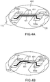
- FIGS. 4A and 4B present perspective views illustrating in a simplified manner interconnection devices according to alternative embodiments of the invention.
- an interconnection device 400 can be formed by a two-wire line comprising two wires 101, 103 in a configuration similar to the configuration described above with reference to figure 1 .
- at least part of the length of the bifilar line for example at least part of the portion of the wires 101, 103 along which they are substantially rectilinear and parallel to one another in this example embodiment, can be globally coated with a dielectric material 401.
- the coating by the dielectric 401 can extend even more widely, for example over the entire length of the wires 101, 103, or even also over the interconnection areas 110a, 110b and 120a, 120b respectively of the two elements to be interconnect 110, 120, that is to say in a region illustrated by the dotted lines in the figure 4A .
- the same characteristics can also be applied to an alternative configuration of the wires 101, 103 in which the wires 101, 103 overlap alternately, like the embodiment described above with reference to figure 3 .
- at least part of the length of the bifilar line for example at least part of the portion of the threads 101, 103 along which the latter are overlapped in this exemplary embodiment, can be generally coated with a material. dielectric 401.
- the coating by the dielectric 401 can extend even more widely, for example over the entire length of the wires 101, 103, or even also over the interconnection areas 110a, 110b and 120a, 120b respectively of the two elements to be interconnect 110, 120, that is to say in a region illustrated by the dotted lines in the figure 4A .
- An interconnection by an interconnection device 400 according to one of the embodiments illustrated by the figures 4A and 4B can be carried out by a method in which an additional coating step, following the aforementioned shaping step, allows the production of the dielectric coating 401.
- the embodiments illustrated by figures 4A and 4B can allow the achievement of characteristic impedances close to or greater than 50 Ohms.
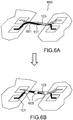
- FIGS. 5A and 5B present perspective views illustrating in a simplified manner interconnection devices according to alternative embodiments of the invention.
- an interconnection device 500 can be formed by a two-wire line comprising two wires 101, 103 in a configuration similar to the configuration described above, for example with reference to figure 1 .
- at least part of the length of each wire 101, 103 for example at least part of the portion of each wire 101, 103 along which the wires 101, 103 are substantially rectilinear and parallel to one another.
- at least one wire can be insulated like the embodiments described above, or even the two wires 101, 103 may not be insulated and simply encased in dielectric material.
- an interconnection device 500 as described above can advantageously comprise one or a plurality of conductive elements 505 arranged in contact with the outer diameters of the wires 101, 103 covered with dielectric material 501, 503.
- the conductive elements 505 make it possible to adjust the impedance matching.
- An interconnection by means of interconnection devices according to the embodiments described above with reference to figures 5B and 6B can be carried out by means of a method comprising, in addition to the aforementioned micro-wiring, shaping and coating steps, an additional step of arranging the conductive elements .
- the conductive elements can for example be arranged by crimping, gluing, welding or by any other suitable technique.
- the two-wire connections are produced exclusively by means of the wires, their insulation and possibly a localized overall coating and / or a dielectric coating and / or conductive elements. These structures in particular do not require the presence of external shielding.
- connections for the interconnection of several elements for example three elements, by means of a plurality of wires having several zones capable of being fixed and electrically connected to the interconnection areas of the elements to be interconnected.
- a two-wire link can be formed by two conductive wires, the ends of each of which are connected to interconnection pads of two first elements to be interconnected, like the embodiments described above, and part of which center of each is stripped so as to be able to be fixed to the connection pads of a third element to be interconnected, disposed substantially between the first two elements to be interconnected.
- Another advantage of the present invention is that it allows interconnection of elements whose interconnection pads are arranged at different heights, for example with respect to the main plane of an electronic circuit board on which the elements to be interconnected. are fixed.
- the interconnection thus produced is also robust with respect to possible variations in temperature which may generate variations in the relative heights or distances of the various elements to be interconnected, or else to vibrations or other mechanical stresses.
Landscapes
- Combinations Of Printed Boards (AREA)
- Structure Of Printed Boards (AREA)
- Waveguide Connection Structure (AREA)
- Wire Bonding (AREA)
Claims (11)
- Verbindungsverfahren für die Übertragung von Mikrowellensignalen zwischen miteinander zu verbindenden Elementen (110, 120) wie elektronischen Modulen oder Schaltkreisen, mit mindestens zwei durch mindestens zwei Drähte (101, 103) gebildeten gekoppelten Leitungen, die mit Verbindungsbereichen (110a, 110b, 120a, 120b) der miteinander zu verbindenden Elemente (110, 120) elektrisch verbunden werden können, wobei mindestens einer der Drähte (101, 103) auf mindestens einem Abschnitt davon mit einem Isolator bedeckt ist, dadurch gekennzeichnet, dass es mindestens einen Mikroverdrahtungsschritt beinhaltet, bei dem die Drähte (101, 103) mit den Verbindungsbereichen (110a, 110b, 120a, 120b) der miteinander zu verbindenden Elemente (110, 120) verbunden werden, gefolgt von einem Schritt des Zueinanderhinbringens und/oder Formens der mindestens zwei Drähte (101, 103), bei dem die mindestens zwei Drähte (101, 103) in ihrer gewünschten Konfiguration angeordnet sind, um eine gewünschte Impedanzanpassung zwischen den miteinander zu verbindenden Elementen (110, 120) zu erzielen.
- Verbindungsverfahren nach Anspruch 1, dadurch gekennzeichnet, dass sich die Drähte (101, 103) nach dem Formungsschritt über mindestens einen Teil ihrer Länge überlappen, über dem mindestens ein Draht durch den Isolator bedeckt ist.
- Verbindungsverfahren nach Anspruch 1, dadurch gekennzeichnet, dass die Drähte (101, 103) nach dem Formungsschritt eine geradlinige Konfiguration aufweisen, wobei die Drähte (101, 103) zumindest auf diesem Abschnitt im Wesentlichen parallel zueinander angeordnet sind.
- Verfahren nach einem der vorhergehenden Ansprüche, dadurch gekennzeichnet, dass die Drähte (101, 103) nach dem Formungsschritt über ihre größte verfügbare Länge zueinander hin gebracht werden.
- Verfahren nach einem der vorhergehenden Ansprüche, dadurch gekennzeichnet, dass auf den Formungsschritt ein Umhüllungsschritt folgt, bei dem mindestens ein Draht (101, 103) über mindestens einen Teil seiner Länge mit einem elektrischen Material (401, 501, 503, 601) umhüllt wird.
- Verbindungsverfahren nach Anspruch 5, dadurch gekennzeichnet, dass das dielektrische Material (401) die mindestens zwei Drähte (101, 103) über mindestens einen Teil ihrer Länge insgesamt umhüllt.
- Verbindungsverfahren nach Anspruch 5, dadurch gekennzeichnet, dass jeder Draht (101, 103) unabhängig über mindestens einen Teil seiner Länge mit dem dielektrischen Material (401) umhüllt ist.
- Verbindungsverfahren nach einem der Ansprüche 5 bis 7, dadurch gekennzeichnet, dass auf den Umhüllungsschritt ein zusätzlicher Schritt des Anordnens von leitenden Elementen (505, 605), die in Kontakt mit den Außendurchmessern der mindestens zwei Drähte (101, 103) sind, zwischen den Drähten (101, 103) folgt, wobei Anzahl und Beschaffenheit der leitenden Elemente (505, 605) so konfiguriert sind, dass sie eine gewünschte Impedanzanpassung der Verbindungsvorrichtung (100, 500) verleihen.
- Werkzeug (200, 300) zum Durchführen eines Verbindungsverfahrens nach einem der vorhergehenden Ansprüche, das einen Kopf umfasst, der sich relativ zu den mindestens zwei Drähten (101, 103) translational und/oder rotational entlang mindestens eines Teils der Länge der mindestens zwei Drähte (101, 103) bewegen kann, wobei das Profil des Kopfs zum Zueinanderhinbringen und/oder Formen der Drähte (101, 103) konfiguriert ist, um sie bei der Bewegung des Kopfs in einer gewünschten Konfiguration zu tragen, um eine gewünschte Impedanzanpassung zwischen den miteinander zu verbindenden Elementen (110, 120) zu erzielen.
- Werkzeug (200) nach Anspruch 9, dadurch gekennzeichnet, dass sich der Kopf relativ zu den mindestens zwei Drähten (101, 103) translational bewegen kann und zwei Nuten (201, 203) umfasst, die jeden der mindestens zwei Drähte (101, 103) aufnehmen können.
- Werkzeug (300) nach Anspruch 9, dadurch gekennzeichnet, dass sich der Kopf relativ zu den mindestens zwei Drähten (101, 103) translational und rotational bewegen kann und zwei zylindrische Stifte (301, 303) umfasst.
Applications Claiming Priority (1)
| Application Number | Priority Date | Filing Date | Title |
|---|---|---|---|
| FR1300465A FR3002814B1 (fr) | 2013-03-01 | 2013-03-01 | Dispositif d'interconnexion pour circuits electroniques par fils paralleles couples, et procede et outillage y relatifs |
Publications (3)
| Publication Number | Publication Date |
|---|---|
| EP2772936A2 EP2772936A2 (de) | 2014-09-03 |
| EP2772936A3 EP2772936A3 (de) | 2017-02-08 |
| EP2772936B1 true EP2772936B1 (de) | 2021-12-29 |
Family
ID=48979790
Family Applications (1)
| Application Number | Title | Priority Date | Filing Date |
|---|---|---|---|
| EP14157235.4A Active EP2772936B1 (de) | 2013-03-01 | 2014-02-28 | Drahtverbindungsverfahren für Paralleldrähte sowie ein Verfahren zur Umformung derselben, sowie die entsprechende Arbeitsgeräte |
Country Status (3)
| Country | Link |
|---|---|
| EP (1) | EP2772936B1 (de) |
| ES (1) | ES2907023T3 (de) |
| FR (1) | FR3002814B1 (de) |
Families Citing this family (2)
| Publication number | Priority date | Publication date | Assignee | Title |
|---|---|---|---|---|
| CN112701092A (zh) * | 2020-12-24 | 2021-04-23 | 北京国联万众半导体科技有限公司 | 毫米波单片集成电路封装结构及其封装方法 |
| WO2025177212A1 (en) * | 2024-02-21 | 2025-08-28 | Baker Hughes Inteq Gmbh | Mechanically coupling multiple wires to improve robustness of wire bond interconnections against mechanical vibrations and shock |
Family Cites Families (10)
| Publication number | Priority date | Publication date | Assignee | Title |
|---|---|---|---|---|
| JP2897086B2 (ja) * | 1991-06-21 | 1999-05-31 | 株式会社村田製作所 | 電子部品へのリード線の位置決め固定方法 |
| JP2763445B2 (ja) * | 1992-04-03 | 1998-06-11 | 三菱電機株式会社 | 高周波信号用配線及びそのボンディング装置 |
| US5459284A (en) * | 1993-08-31 | 1995-10-17 | Motorola, Inc. | Twisted-pair wire bond and method thereof |
| JP2000323907A (ja) * | 1999-05-07 | 2000-11-24 | Nec Corp | マイクロ波ic接続線路 |
| JP3915723B2 (ja) * | 2003-03-25 | 2007-05-16 | 株式会社デンソー | ワイヤボンディング方法 |
| JP2005064248A (ja) * | 2003-08-12 | 2005-03-10 | Renesas Technology Corp | 半導体装置およびその製造方法 |
| US6992377B2 (en) * | 2004-02-26 | 2006-01-31 | Freescale Semiconductor, Inc. | Semiconductor package with crossing conductor assembly and method of manufacture |
| US20060175712A1 (en) * | 2005-02-10 | 2006-08-10 | Microbonds, Inc. | High performance IC package and method |
| US7741720B2 (en) * | 2007-09-25 | 2010-06-22 | Silverbrook Research Pty Ltd | Electronic device with wire bonds adhered between integrated circuits dies and printed circuit boards |
| JP2009158839A (ja) * | 2007-12-27 | 2009-07-16 | Sharp Corp | 半導体パッケージ、半導体装置、およびワイヤボンディング方法 |
-
2013
- 2013-03-01 FR FR1300465A patent/FR3002814B1/fr not_active Expired - Fee Related
-
2014
- 2014-02-28 ES ES14157235T patent/ES2907023T3/es active Active
- 2014-02-28 EP EP14157235.4A patent/EP2772936B1/de active Active
Also Published As
| Publication number | Publication date |
|---|---|
| FR3002814A1 (fr) | 2014-09-05 |
| EP2772936A3 (de) | 2017-02-08 |
| FR3002814B1 (fr) | 2016-06-24 |
| ES2907023T3 (es) | 2022-04-21 |
| EP2772936A2 (de) | 2014-09-03 |
Similar Documents
| Publication | Publication Date | Title |
|---|---|---|
| EP1062634B1 (de) | Chipkarte mit einer schleifenantenne und zugehöriges mikromodul | |
| FR2945895A1 (fr) | Dispositif d'interconnexion pour circuits electroniques, notamment des circuits electroniques hyperfrequence | |
| EP0734063A2 (de) | Mikromodul einer integrierten Schaltung durch ein kontinuierliches Zusammenfügen von gemusterten Bändern hergestellt | |
| EP4057039B1 (de) | Optoelektronische vorrichtung mit einem aktiven photonischen zwischenträger, an den ein mikroelektronischer chip und ein elektrooptischer umwandlungschip angeschlossen sind | |
| EP2158604A2 (de) | Zusammenbau von hochfrequenzchips | |
| FR2596607A1 (fr) | Procede de montage d'un circuit integre sur une carte de circuits imprimes, boitier de circuit integre en resultant et ruban porteur de circuits integres pour la mise en oeuvre du procede | |
| EP3579286B1 (de) | Photonenchip, der von einer leitung durchzogen wird | |
| EP0424262B1 (de) | Tragbare, mit Bausteinen verbindbare Elektronik | |
| FR3007403A1 (fr) | Procede de realisation d'un dispositif microelectronique mecaniquement autonome | |
| EP2747528B1 (de) | Vorrichtung zum Verbinden von elektronischen Schaltkreisen, insbesondere von elektronischen Höchstfrequenzschaltkreisen | |
| EP0044247B1 (de) | Verfahren zur Herstellung eines Trägers für elektronische Elemente zur Verbindung integrierter Halbleiteranordnungen | |
| EP2772936B1 (de) | Drahtverbindungsverfahren für Paralleldrähte sowie ein Verfahren zur Umformung derselben, sowie die entsprechende Arbeitsgeräte | |
| EP0353114B1 (de) | Verbindungsvorrichtung zwischen einer integrierten Schaltung und einer elektrischen Schaltung und Herstellungsverfahren derselben | |
| EP2273425A1 (de) | Verfahren zur elektrischen Verbindung von zwei Elementen | |
| FR2963849A1 (fr) | Procede de fabrication d'un circuit electrique et circuit obtenu | |
| CA2968070A1 (fr) | Procede de fabrication d'un module electronique simple face comprenant des zones d'interconnexion | |
| FR2547112A1 (fr) | Procede de realisation d'un circuit hybride et circuit hybride logique ou analogique | |
| EP2162908B1 (de) | Herstellungsverfahren eines rekonstituierten elektronischen bauelements und entsprechendes rekonstituiertes elektronisches bauelement | |
| EP0969410B1 (de) | Chipkarte mit Antenne | |
| EP1192593A1 (de) | Vorrichtung und herstellungsverfahren mit zumindest einem chip auf einem träger | |
| EP3109899B1 (de) | Elektronisches 3d-modul, das einen bga-stapel umfasst | |
| CN104142541B (zh) | 光布线基板、光布线基板的制造方法、以及光学模块 | |
| FR2795200A1 (fr) | Dispositif electronique comportant au moins une puce fixee sur un support et procede de fabrication d'un tel dispositif | |
| EP4625478A1 (de) | Verfahren zum zusammenbau einer integrierten schaltung in vertikaler richtung und bauelement mit integrierter vertikaler schaltung | |
| EP2391191A1 (de) | Vorrichtung zum Verbinden von elektronischen Schaltkreisen, insbesondere von elektronischen Hyperfrequenzschaltkreisen |
Legal Events
| Date | Code | Title | Description |
|---|---|---|---|
| PUAI | Public reference made under article 153(3) epc to a published international application that has entered the european phase |
Free format text: ORIGINAL CODE: 0009012 |
|
| 17P | Request for examination filed |
Effective date: 20140228 |
|
| AK | Designated contracting states |
Kind code of ref document: A2 Designated state(s): AL AT BE BG CH CY CZ DE DK EE ES FI FR GB GR HR HU IE IS IT LI LT LU LV MC MK MT NL NO PL PT RO RS SE SI SK SM TR |
|
| AX | Request for extension of the european patent |
Extension state: BA ME |
|
| PUAL | Search report despatched |
Free format text: ORIGINAL CODE: 0009013 |
|
| AK | Designated contracting states |
Kind code of ref document: A3 Designated state(s): AL AT BE BG CH CY CZ DE DK EE ES FI FR GB GR HR HU IE IS IT LI LT LU LV MC MK MT NL NO PL PT RO RS SE SI SK SM TR |
|
| AX | Request for extension of the european patent |
Extension state: BA ME |
|
| RIC1 | Information provided on ipc code assigned before grant |
Ipc: H01L 23/49 20060101AFI20170103BHEP Ipc: H01L 23/66 20060101ALI20170103BHEP |
|
| STAA | Information on the status of an ep patent application or granted ep patent |
Free format text: STATUS: REQUEST FOR EXAMINATION WAS MADE |
|
| R17P | Request for examination filed (corrected) |
Effective date: 20170807 |
|
| RBV | Designated contracting states (corrected) |
Designated state(s): AL AT BE BG CH CY CZ DE DK EE ES FI FR GB GR HR HU IE IS IT LI LT LU LV MC MK MT NL NO PL PT RO RS SE SI SK SM TR |
|
| STAA | Information on the status of an ep patent application or granted ep patent |
Free format text: STATUS: EXAMINATION IS IN PROGRESS |
|
| 17Q | First examination report despatched |
Effective date: 20210309 |
|
| GRAP | Despatch of communication of intention to grant a patent |
Free format text: ORIGINAL CODE: EPIDOSNIGR1 |
|
| STAA | Information on the status of an ep patent application or granted ep patent |
Free format text: STATUS: GRANT OF PATENT IS INTENDED |
|
| INTG | Intention to grant announced |
Effective date: 20210802 |
|
| GRAS | Grant fee paid |
Free format text: ORIGINAL CODE: EPIDOSNIGR3 |
|
| GRAA | (expected) grant |
Free format text: ORIGINAL CODE: 0009210 |
|
| STAA | Information on the status of an ep patent application or granted ep patent |
Free format text: STATUS: THE PATENT HAS BEEN GRANTED |
|
| RAP3 | Party data changed (applicant data changed or rights of an application transferred) |
Owner name: THALES |
|
| AK | Designated contracting states |
Kind code of ref document: B1 Designated state(s): AL AT BE BG CH CY CZ DE DK EE ES FI FR GB GR HR HU IE IS IT LI LT LU LV MC MK MT NL NO PL PT RO RS SE SI SK SM TR |
|
| REG | Reference to a national code |
Ref country code: GB Ref legal event code: FG4D Free format text: NOT ENGLISH |
|
| REG | Reference to a national code |
Ref country code: CH Ref legal event code: EP |
|
| REG | Reference to a national code |
Ref country code: AT Ref legal event code: REF Ref document number: 1459322 Country of ref document: AT Kind code of ref document: T Effective date: 20220115 |
|
| REG | Reference to a national code |
Ref country code: IE Ref legal event code: FG4D Free format text: LANGUAGE OF EP DOCUMENT: FRENCH |
|
| REG | Reference to a national code |
Ref country code: DE Ref legal event code: R096 Ref document number: 602014081889 Country of ref document: DE |
|
| REG | Reference to a national code |
Ref country code: NL Ref legal event code: FP |
|
| REG | Reference to a national code |
Ref country code: LT Ref legal event code: MG9D |
|
| REG | Reference to a national code |
Ref country code: ES Ref legal event code: FG2A Ref document number: 2907023 Country of ref document: ES Kind code of ref document: T3 Effective date: 20220421 |
|
| PG25 | Lapsed in a contracting state [announced via postgrant information from national office to epo] |
Ref country code: RS Free format text: LAPSE BECAUSE OF FAILURE TO SUBMIT A TRANSLATION OF THE DESCRIPTION OR TO PAY THE FEE WITHIN THE PRESCRIBED TIME-LIMIT Effective date: 20211229 Ref country code: LT Free format text: LAPSE BECAUSE OF FAILURE TO SUBMIT A TRANSLATION OF THE DESCRIPTION OR TO PAY THE FEE WITHIN THE PRESCRIBED TIME-LIMIT Effective date: 20211229 Ref country code: FI Free format text: LAPSE BECAUSE OF FAILURE TO SUBMIT A TRANSLATION OF THE DESCRIPTION OR TO PAY THE FEE WITHIN THE PRESCRIBED TIME-LIMIT Effective date: 20211229 Ref country code: BG Free format text: LAPSE BECAUSE OF FAILURE TO SUBMIT A TRANSLATION OF THE DESCRIPTION OR TO PAY THE FEE WITHIN THE PRESCRIBED TIME-LIMIT Effective date: 20220329 |
|
| REG | Reference to a national code |
Ref country code: AT Ref legal event code: MK05 Ref document number: 1459322 Country of ref document: AT Kind code of ref document: T Effective date: 20211229 |
|
| PG25 | Lapsed in a contracting state [announced via postgrant information from national office to epo] |
Ref country code: SE Free format text: LAPSE BECAUSE OF FAILURE TO SUBMIT A TRANSLATION OF THE DESCRIPTION OR TO PAY THE FEE WITHIN THE PRESCRIBED TIME-LIMIT Effective date: 20211229 Ref country code: NO Free format text: LAPSE BECAUSE OF FAILURE TO SUBMIT A TRANSLATION OF THE DESCRIPTION OR TO PAY THE FEE WITHIN THE PRESCRIBED TIME-LIMIT Effective date: 20220329 Ref country code: LV Free format text: LAPSE BECAUSE OF FAILURE TO SUBMIT A TRANSLATION OF THE DESCRIPTION OR TO PAY THE FEE WITHIN THE PRESCRIBED TIME-LIMIT Effective date: 20211229 Ref country code: HR Free format text: LAPSE BECAUSE OF FAILURE TO SUBMIT A TRANSLATION OF THE DESCRIPTION OR TO PAY THE FEE WITHIN THE PRESCRIBED TIME-LIMIT Effective date: 20211229 Ref country code: GR Free format text: LAPSE BECAUSE OF FAILURE TO SUBMIT A TRANSLATION OF THE DESCRIPTION OR TO PAY THE FEE WITHIN THE PRESCRIBED TIME-LIMIT Effective date: 20220330 |
|
| PG25 | Lapsed in a contracting state [announced via postgrant information from national office to epo] |
Ref country code: SM Free format text: LAPSE BECAUSE OF FAILURE TO SUBMIT A TRANSLATION OF THE DESCRIPTION OR TO PAY THE FEE WITHIN THE PRESCRIBED TIME-LIMIT Effective date: 20211229 Ref country code: SK Free format text: LAPSE BECAUSE OF FAILURE TO SUBMIT A TRANSLATION OF THE DESCRIPTION OR TO PAY THE FEE WITHIN THE PRESCRIBED TIME-LIMIT Effective date: 20211229 Ref country code: RO Free format text: LAPSE BECAUSE OF FAILURE TO SUBMIT A TRANSLATION OF THE DESCRIPTION OR TO PAY THE FEE WITHIN THE PRESCRIBED TIME-LIMIT Effective date: 20211229 Ref country code: PT Free format text: LAPSE BECAUSE OF FAILURE TO SUBMIT A TRANSLATION OF THE DESCRIPTION OR TO PAY THE FEE WITHIN THE PRESCRIBED TIME-LIMIT Effective date: 20220429 Ref country code: EE Free format text: LAPSE BECAUSE OF FAILURE TO SUBMIT A TRANSLATION OF THE DESCRIPTION OR TO PAY THE FEE WITHIN THE PRESCRIBED TIME-LIMIT Effective date: 20211229 Ref country code: CZ Free format text: LAPSE BECAUSE OF FAILURE TO SUBMIT A TRANSLATION OF THE DESCRIPTION OR TO PAY THE FEE WITHIN THE PRESCRIBED TIME-LIMIT Effective date: 20211229 |
|
| PG25 | Lapsed in a contracting state [announced via postgrant information from national office to epo] |
Ref country code: PL Free format text: LAPSE BECAUSE OF FAILURE TO SUBMIT A TRANSLATION OF THE DESCRIPTION OR TO PAY THE FEE WITHIN THE PRESCRIBED TIME-LIMIT Effective date: 20211229 Ref country code: AT Free format text: LAPSE BECAUSE OF FAILURE TO SUBMIT A TRANSLATION OF THE DESCRIPTION OR TO PAY THE FEE WITHIN THE PRESCRIBED TIME-LIMIT Effective date: 20211229 |
|
| PG25 | Lapsed in a contracting state [announced via postgrant information from national office to epo] |
Ref country code: MC Free format text: LAPSE BECAUSE OF FAILURE TO SUBMIT A TRANSLATION OF THE DESCRIPTION OR TO PAY THE FEE WITHIN THE PRESCRIBED TIME-LIMIT Effective date: 20211229 Ref country code: IS Free format text: LAPSE BECAUSE OF FAILURE TO SUBMIT A TRANSLATION OF THE DESCRIPTION OR TO PAY THE FEE WITHIN THE PRESCRIBED TIME-LIMIT Effective date: 20220429 |
|
| REG | Reference to a national code |
Ref country code: DE Ref legal event code: R097 Ref document number: 602014081889 Country of ref document: DE |
|
| REG | Reference to a national code |
Ref country code: CH Ref legal event code: PL |
|
| PG25 | Lapsed in a contracting state [announced via postgrant information from national office to epo] |
Ref country code: LU Free format text: LAPSE BECAUSE OF NON-PAYMENT OF DUE FEES Effective date: 20220228 Ref country code: DK Free format text: LAPSE BECAUSE OF FAILURE TO SUBMIT A TRANSLATION OF THE DESCRIPTION OR TO PAY THE FEE WITHIN THE PRESCRIBED TIME-LIMIT Effective date: 20211229 Ref country code: AL Free format text: LAPSE BECAUSE OF FAILURE TO SUBMIT A TRANSLATION OF THE DESCRIPTION OR TO PAY THE FEE WITHIN THE PRESCRIBED TIME-LIMIT Effective date: 20211229 |
|
| PLBE | No opposition filed within time limit |
Free format text: ORIGINAL CODE: 0009261 |
|
| STAA | Information on the status of an ep patent application or granted ep patent |
Free format text: STATUS: NO OPPOSITION FILED WITHIN TIME LIMIT |
|
| 26N | No opposition filed |
Effective date: 20220930 |
|
| PG25 | Lapsed in a contracting state [announced via postgrant information from national office to epo] |
Ref country code: LI Free format text: LAPSE BECAUSE OF NON-PAYMENT OF DUE FEES Effective date: 20220228 Ref country code: IE Free format text: LAPSE BECAUSE OF NON-PAYMENT OF DUE FEES Effective date: 20220228 Ref country code: CH Free format text: LAPSE BECAUSE OF NON-PAYMENT OF DUE FEES Effective date: 20220228 |
|
| PG25 | Lapsed in a contracting state [announced via postgrant information from national office to epo] |
Ref country code: SI Free format text: LAPSE BECAUSE OF FAILURE TO SUBMIT A TRANSLATION OF THE DESCRIPTION OR TO PAY THE FEE WITHIN THE PRESCRIBED TIME-LIMIT Effective date: 20211229 |
|
| PG25 | Lapsed in a contracting state [announced via postgrant information from national office to epo] |
Ref country code: HU Free format text: LAPSE BECAUSE OF FAILURE TO SUBMIT A TRANSLATION OF THE DESCRIPTION OR TO PAY THE FEE WITHIN THE PRESCRIBED TIME-LIMIT; INVALID AB INITIO Effective date: 20140228 |
|
| PG25 | Lapsed in a contracting state [announced via postgrant information from national office to epo] |
Ref country code: MK Free format text: LAPSE BECAUSE OF FAILURE TO SUBMIT A TRANSLATION OF THE DESCRIPTION OR TO PAY THE FEE WITHIN THE PRESCRIBED TIME-LIMIT Effective date: 20211229 Ref country code: CY Free format text: LAPSE BECAUSE OF FAILURE TO SUBMIT A TRANSLATION OF THE DESCRIPTION OR TO PAY THE FEE WITHIN THE PRESCRIBED TIME-LIMIT Effective date: 20211229 |
|
| PG25 | Lapsed in a contracting state [announced via postgrant information from national office to epo] |
Ref country code: MT Free format text: LAPSE BECAUSE OF FAILURE TO SUBMIT A TRANSLATION OF THE DESCRIPTION OR TO PAY THE FEE WITHIN THE PRESCRIBED TIME-LIMIT Effective date: 20211229 |
|
| REG | Reference to a national code |
Ref country code: DE Ref legal event code: R079 Ref document number: 602014081889 Country of ref document: DE Free format text: PREVIOUS MAIN CLASS: H01L0023490000 Ipc: H10W0072500000 |
|
| PG25 | Lapsed in a contracting state [announced via postgrant information from national office to epo] |
Ref country code: TR Free format text: LAPSE BECAUSE OF FAILURE TO SUBMIT A TRANSLATION OF THE DESCRIPTION OR TO PAY THE FEE WITHIN THE PRESCRIBED TIME-LIMIT Effective date: 20211229 |
|
| PGFP | Annual fee paid to national office [announced via postgrant information from national office to epo] |
Ref country code: NL Payment date: 20260128 Year of fee payment: 13 |
|
| PGFP | Annual fee paid to national office [announced via postgrant information from national office to epo] |
Ref country code: GB Payment date: 20260119 Year of fee payment: 13 |
|
| PGFP | Annual fee paid to national office [announced via postgrant information from national office to epo] |
Ref country code: ES Payment date: 20260305 Year of fee payment: 13 |
|
| PGFP | Annual fee paid to national office [announced via postgrant information from national office to epo] |
Ref country code: DE Payment date: 20260114 Year of fee payment: 13 |
|
| PGFP | Annual fee paid to national office [announced via postgrant information from national office to epo] |
Ref country code: IT Payment date: 20260128 Year of fee payment: 13 Ref country code: BE Payment date: 20260113 Year of fee payment: 13 |
|
| PGFP | Annual fee paid to national office [announced via postgrant information from national office to epo] |
Ref country code: FR Payment date: 20260121 Year of fee payment: 13 |