EP2779246A2 - Procédé de formation d'un dispositif semi-conducteur à haute mobilité d'électrons et structure associée - Google Patents
Procédé de formation d'un dispositif semi-conducteur à haute mobilité d'électrons et structure associée Download PDFInfo
- Publication number
- EP2779246A2 EP2779246A2 EP14159610.6A EP14159610A EP2779246A2 EP 2779246 A2 EP2779246 A2 EP 2779246A2 EP 14159610 A EP14159610 A EP 14159610A EP 2779246 A2 EP2779246 A2 EP 2779246A2
- Authority
- EP
- European Patent Office
- Prior art keywords
- base substrate
- forming
- barrier layer
- internal conductor
- conductor structure
- Prior art date
- Legal status (The legal status is an assumption and is not a legal conclusion. Google has not performed a legal analysis and makes no representation as to the accuracy of the status listed.)
- Ceased
Links
Images





Classifications
-
- H—ELECTRICITY
- H10—SEMICONDUCTOR DEVICES; ELECTRIC SOLID-STATE DEVICES NOT OTHERWISE PROVIDED FOR
- H10D—INORGANIC ELECTRIC SEMICONDUCTOR DEVICES
- H10D84/00—Integrated devices formed in or on semiconductor substrates that comprise only semiconducting layers, e.g. on Si wafers or on GaAs-on-Si wafers
- H10D84/40—Integrated devices formed in or on semiconductor substrates that comprise only semiconducting layers, e.g. on Si wafers or on GaAs-on-Si wafers characterised by the integration of at least one component covered by groups H10D12/00 or H10D30/00 with at least one component covered by groups H10D10/00 or H10D18/00, e.g. integration of IGFETs with BJTs
-
- H—ELECTRICITY
- H10—SEMICONDUCTOR DEVICES; ELECTRIC SOLID-STATE DEVICES NOT OTHERWISE PROVIDED FOR
- H10D—INORGANIC ELECTRIC SEMICONDUCTOR DEVICES
- H10D30/00—Field-effect transistors [FET]
- H10D30/01—Manufacture or treatment
- H10D30/015—Manufacture or treatment of FETs having heterojunction interface channels or heterojunction gate electrodes, e.g. HEMT
-
- H—ELECTRICITY
- H10—SEMICONDUCTOR DEVICES; ELECTRIC SOLID-STATE DEVICES NOT OTHERWISE PROVIDED FOR
- H10D—INORGANIC ELECTRIC SEMICONDUCTOR DEVICES
- H10D30/00—Field-effect transistors [FET]
- H10D30/40—FETs having zero-dimensional [0D], one-dimensional [1D] or two-dimensional [2D] charge carrier gas channels
- H10D30/47—FETs having zero-dimensional [0D], one-dimensional [1D] or two-dimensional [2D] charge carrier gas channels having two-dimensional [2D] charge carrier gas channels, e.g. nanoribbon FETs or high electron mobility transistors [HEMT]
- H10D30/471—High electron mobility transistors [HEMT] or high hole mobility transistors [HHMT]
- H10D30/475—High electron mobility transistors [HEMT] or high hole mobility transistors [HHMT] having wider bandgap layer formed on top of lower bandgap active layer, e.g. undoped barrier HEMTs such as i-AlGaN/GaN HEMTs
-
- H—ELECTRICITY
- H10—SEMICONDUCTOR DEVICES; ELECTRIC SOLID-STATE DEVICES NOT OTHERWISE PROVIDED FOR
- H10D—INORGANIC ELECTRIC SEMICONDUCTOR DEVICES
- H10D30/00—Field-effect transistors [FET]
- H10D30/40—FETs having zero-dimensional [0D], one-dimensional [1D] or two-dimensional [2D] charge carrier gas channels
- H10D30/47—FETs having zero-dimensional [0D], one-dimensional [1D] or two-dimensional [2D] charge carrier gas channels having two-dimensional [2D] charge carrier gas channels, e.g. nanoribbon FETs or high electron mobility transistors [HEMT]
- H10D30/471—High electron mobility transistors [HEMT] or high hole mobility transistors [HHMT]
- H10D30/475—High electron mobility transistors [HEMT] or high hole mobility transistors [HHMT] having wider bandgap layer formed on top of lower bandgap active layer, e.g. undoped barrier HEMTs such as i-AlGaN/GaN HEMTs
- H10D30/4755—High electron mobility transistors [HEMT] or high hole mobility transistors [HHMT] having wider bandgap layer formed on top of lower bandgap active layer, e.g. undoped barrier HEMTs such as i-AlGaN/GaN HEMTs having wide bandgap charge-carrier supplying layers, e.g. modulation doped HEMTs such as n-AlGaAs/GaAs HEMTs
-
- H—ELECTRICITY
- H10—SEMICONDUCTOR DEVICES; ELECTRIC SOLID-STATE DEVICES NOT OTHERWISE PROVIDED FOR
- H10D—INORGANIC ELECTRIC SEMICONDUCTOR DEVICES
- H10D30/00—Field-effect transistors [FET]
- H10D30/40—FETs having zero-dimensional [0D], one-dimensional [1D] or two-dimensional [2D] charge carrier gas channels
- H10D30/47—FETs having zero-dimensional [0D], one-dimensional [1D] or two-dimensional [2D] charge carrier gas channels having two-dimensional [2D] charge carrier gas channels, e.g. nanoribbon FETs or high electron mobility transistors [HEMT]
- H10D30/471—High electron mobility transistors [HEMT] or high hole mobility transistors [HHMT]
- H10D30/477—Vertical HEMTs or vertical HHMTs
-
- H—ELECTRICITY
- H10—SEMICONDUCTOR DEVICES; ELECTRIC SOLID-STATE DEVICES NOT OTHERWISE PROVIDED FOR
- H10D—INORGANIC ELECTRIC SEMICONDUCTOR DEVICES
- H10D30/00—Field-effect transistors [FET]
- H10D30/60—Insulated-gate field-effect transistors [IGFET]
- H10D30/63—Vertical IGFETs
-
- H—ELECTRICITY
- H10—SEMICONDUCTOR DEVICES; ELECTRIC SOLID-STATE DEVICES NOT OTHERWISE PROVIDED FOR
- H10D—INORGANIC ELECTRIC SEMICONDUCTOR DEVICES
- H10D62/00—Semiconductor bodies, or regions thereof, of devices having potential barriers
- H10D62/80—Semiconductor bodies, or regions thereof, of devices having potential barriers characterised by the materials
- H10D62/82—Heterojunctions
- H10D62/824—Heterojunctions comprising only Group III-V materials heterojunctions, e.g. GaN/AlGaN heterojunctions
-
- H—ELECTRICITY
- H10—SEMICONDUCTOR DEVICES; ELECTRIC SOLID-STATE DEVICES NOT OTHERWISE PROVIDED FOR
- H10D—INORGANIC ELECTRIC SEMICONDUCTOR DEVICES
- H10D64/00—Electrodes of devices having potential barriers
- H10D64/111—Field plates
- H10D64/117—Recessed field plates, e.g. trench field plates or buried field plates
-
- H—ELECTRICITY
- H10—SEMICONDUCTOR DEVICES; ELECTRIC SOLID-STATE DEVICES NOT OTHERWISE PROVIDED FOR
- H10D—INORGANIC ELECTRIC SEMICONDUCTOR DEVICES
- H10D64/00—Electrodes of devices having potential barriers
- H10D64/20—Electrodes characterised by their shapes, relative sizes or dispositions
- H10D64/23—Electrodes carrying the current to be rectified, amplified, oscillated or switched, e.g. sources, drains, anodes or cathodes
- H10D64/251—Source or drain electrodes for field-effect devices
- H10D64/254—Source or drain electrodes for field-effect devices for lateral devices wherein the source or drain electrodes extend entirely through the semiconductor bodies, e.g. via-holes for back side contacts
-
- H—ELECTRICITY
- H10—SEMICONDUCTOR DEVICES; ELECTRIC SOLID-STATE DEVICES NOT OTHERWISE PROVIDED FOR
- H10D—INORGANIC ELECTRIC SEMICONDUCTOR DEVICES
- H10D64/00—Electrodes of devices having potential barriers
- H10D64/20—Electrodes characterised by their shapes, relative sizes or dispositions
- H10D64/27—Electrodes not carrying the current to be rectified, amplified, oscillated or switched, e.g. gates
- H10D64/311—Gate electrodes for field-effect devices
- H10D64/411—Gate electrodes for field-effect devices for FETs
- H10D64/511—Gate electrodes for field-effect devices for FETs for IGFETs
- H10D64/512—Disposition of the gate electrodes, e.g. buried gates
- H10D64/513—Disposition of the gate electrodes, e.g. buried gates within recesses in the substrate, e.g. trench gates, groove gates or buried gates
-
- H—ELECTRICITY
- H10—SEMICONDUCTOR DEVICES; ELECTRIC SOLID-STATE DEVICES NOT OTHERWISE PROVIDED FOR
- H10D—INORGANIC ELECTRIC SEMICONDUCTOR DEVICES
- H10D8/00—Diodes
- H10D8/60—Schottky-barrier diodes
-
- H—ELECTRICITY
- H10—SEMICONDUCTOR DEVICES; ELECTRIC SOLID-STATE DEVICES NOT OTHERWISE PROVIDED FOR
- H10D—INORGANIC ELECTRIC SEMICONDUCTOR DEVICES
- H10D84/00—Integrated devices formed in or on semiconductor substrates that comprise only semiconducting layers, e.g. on Si wafers or on GaAs-on-Si wafers
- H10D84/01—Manufacture or treatment
-
- H—ELECTRICITY
- H10—SEMICONDUCTOR DEVICES; ELECTRIC SOLID-STATE DEVICES NOT OTHERWISE PROVIDED FOR
- H10D—INORGANIC ELECTRIC SEMICONDUCTOR DEVICES
- H10D84/00—Integrated devices formed in or on semiconductor substrates that comprise only semiconducting layers, e.g. on Si wafers or on GaAs-on-Si wafers
- H10D84/01—Manufacture or treatment
- H10D84/02—Manufacture or treatment characterised by using material-based technologies
- H10D84/05—Manufacture or treatment characterised by using material-based technologies using Group III-V technology
-
- H—ELECTRICITY
- H10—SEMICONDUCTOR DEVICES; ELECTRIC SOLID-STATE DEVICES NOT OTHERWISE PROVIDED FOR
- H10W—GENERIC PACKAGES, INTERCONNECTIONS, CONNECTORS OR OTHER CONSTRUCTIONAL DETAILS OF DEVICES COVERED BY CLASS H10
- H10W70/00—Package substrates; Interposers; Redistribution layers [RDL]
- H10W70/40—Leadframes
- H10W70/411—Chip-supporting parts, e.g. die pads
-
- H—ELECTRICITY
- H10—SEMICONDUCTOR DEVICES; ELECTRIC SOLID-STATE DEVICES NOT OTHERWISE PROVIDED FOR
- H10W—GENERIC PACKAGES, INTERCONNECTIONS, CONNECTORS OR OTHER CONSTRUCTIONAL DETAILS OF DEVICES COVERED BY CLASS H10
- H10W70/00—Package substrates; Interposers; Redistribution layers [RDL]
- H10W70/40—Leadframes
- H10W70/481—Leadframes for devices being provided for in groups H10D8/00 - H10D48/00
-
- H—ELECTRICITY
- H10—SEMICONDUCTOR DEVICES; ELECTRIC SOLID-STATE DEVICES NOT OTHERWISE PROVIDED FOR
- H10W—GENERIC PACKAGES, INTERCONNECTIONS, CONNECTORS OR OTHER CONSTRUCTIONAL DETAILS OF DEVICES COVERED BY CLASS H10
- H10W74/00—Encapsulations, e.g. protective coatings
- H10W74/10—Encapsulations, e.g. protective coatings characterised by their shape or disposition
- H10W74/111—Encapsulations, e.g. protective coatings characterised by their shape or disposition the semiconductor body being completely enclosed
-
- H—ELECTRICITY
- H10—SEMICONDUCTOR DEVICES; ELECTRIC SOLID-STATE DEVICES NOT OTHERWISE PROVIDED FOR
- H10W—GENERIC PACKAGES, INTERCONNECTIONS, CONNECTORS OR OTHER CONSTRUCTIONAL DETAILS OF DEVICES COVERED BY CLASS H10
- H10W90/00—Package configurations
- H10W90/811—Multiple chips on leadframes
-
- H—ELECTRICITY
- H10—SEMICONDUCTOR DEVICES; ELECTRIC SOLID-STATE DEVICES NOT OTHERWISE PROVIDED FOR
- H10D—INORGANIC ELECTRIC SEMICONDUCTOR DEVICES
- H10D62/00—Semiconductor bodies, or regions thereof, of devices having potential barriers
- H10D62/10—Shapes, relative sizes or dispositions of the regions of the semiconductor bodies; Shapes of the semiconductor bodies
- H10D62/17—Semiconductor regions connected to electrodes not carrying current to be rectified, amplified or switched, e.g. channel regions
- H10D62/351—Substrate regions of field-effect devices
- H10D62/357—Substrate regions of field-effect devices of FETs
- H10D62/364—Substrate regions of field-effect devices of FETs of IGFETs
- H10D62/378—Contact regions to the substrate regions
-
- H—ELECTRICITY
- H10—SEMICONDUCTOR DEVICES; ELECTRIC SOLID-STATE DEVICES NOT OTHERWISE PROVIDED FOR
- H10D—INORGANIC ELECTRIC SEMICONDUCTOR DEVICES
- H10D62/00—Semiconductor bodies, or regions thereof, of devices having potential barriers
- H10D62/80—Semiconductor bodies, or regions thereof, of devices having potential barriers characterised by the materials
- H10D62/85—Semiconductor bodies, or regions thereof, of devices having potential barriers characterised by the materials being Group III-V materials, e.g. GaAs
- H10D62/8503—Nitride Group III-V materials, e.g. AlN or GaN
-
- H—ELECTRICITY
- H10—SEMICONDUCTOR DEVICES; ELECTRIC SOLID-STATE DEVICES NOT OTHERWISE PROVIDED FOR
- H10D—INORGANIC ELECTRIC SEMICONDUCTOR DEVICES
- H10D64/00—Electrodes of devices having potential barriers
- H10D64/20—Electrodes characterised by their shapes, relative sizes or dispositions
- H10D64/23—Electrodes carrying the current to be rectified, amplified, oscillated or switched, e.g. sources, drains, anodes or cathodes
- H10D64/251—Source or drain electrodes for field-effect devices
- H10D64/256—Source or drain electrodes for field-effect devices for lateral devices wherein the source or drain electrodes are recessed in semiconductor bodies
-
- H—ELECTRICITY
- H10—SEMICONDUCTOR DEVICES; ELECTRIC SOLID-STATE DEVICES NOT OTHERWISE PROVIDED FOR
- H10D—INORGANIC ELECTRIC SEMICONDUCTOR DEVICES
- H10D64/00—Electrodes of devices having potential barriers
- H10D64/20—Electrodes characterised by their shapes, relative sizes or dispositions
- H10D64/23—Electrodes carrying the current to be rectified, amplified, oscillated or switched, e.g. sources, drains, anodes or cathodes
- H10D64/251—Source or drain electrodes for field-effect devices
- H10D64/258—Source or drain electrodes for field-effect devices characterised by the relative positions of the source or drain electrodes with respect to the gate electrode
-
- H—ELECTRICITY
- H10—SEMICONDUCTOR DEVICES; ELECTRIC SOLID-STATE DEVICES NOT OTHERWISE PROVIDED FOR
- H10W—GENERIC PACKAGES, INTERCONNECTIONS, CONNECTORS OR OTHER CONSTRUCTIONAL DETAILS OF DEVICES COVERED BY CLASS H10
- H10W72/00—Interconnections or connectors in packages
- H10W72/90—Bond pads, in general
- H10W72/921—Structures or relative sizes of bond pads
- H10W72/926—Multiple bond pads having different sizes
-
- H—ELECTRICITY
- H10—SEMICONDUCTOR DEVICES; ELECTRIC SOLID-STATE DEVICES NOT OTHERWISE PROVIDED FOR
- H10W—GENERIC PACKAGES, INTERCONNECTIONS, CONNECTORS OR OTHER CONSTRUCTIONAL DETAILS OF DEVICES COVERED BY CLASS H10
- H10W72/00—Interconnections or connectors in packages
- H10W72/90—Bond pads, in general
- H10W72/981—Auxiliary members, e.g. spacers
- H10W72/983—Reinforcing structures, e.g. collars
-
- H—ELECTRICITY
- H10—SEMICONDUCTOR DEVICES; ELECTRIC SOLID-STATE DEVICES NOT OTHERWISE PROVIDED FOR
- H10W—GENERIC PACKAGES, INTERCONNECTIONS, CONNECTORS OR OTHER CONSTRUCTIONAL DETAILS OF DEVICES COVERED BY CLASS H10
- H10W90/00—Package configurations
- H10W90/701—Package configurations characterised by the relative positions of pads or connectors relative to package parts
- H10W90/751—Package configurations characterised by the relative positions of pads or connectors relative to package parts of bond wires
- H10W90/756—Package configurations characterised by the relative positions of pads or connectors relative to package parts of bond wires between a chip and a stacked lead frame, conducting package substrate or heat sink
Definitions
- the present invention relates, in general, to electronics, and more particularly, to semiconductors, structures thereof, and methods of forming semiconductor devices.
- the semiconductor industry utilized various methods to form power semiconductor devices that used at least one III series semiconductor material, such as gallium nitride (GaN), as one of the semiconductor materials.
- III series semiconductor material such as gallium nitride (GaN)
- Such power semiconductor devices were used in a variety of applications including power supplies and motor controllers including high voltage switching circuits.
- GaN power semiconductor devices built on silicon substrates such as high electron mobility transistor (“HEMT”) devices, have been lateral devices with both the source and drain electrodes on the top surface of the device.
- HEMT high electron mobility transistor
- MOS silicon metal-oxide-semiconductor
- GaN or other III series materials such as a III-nitride series material or SiC that has improved connect device ability as well as integration capability.
- the method includes forming the first internal conductor structure includes forming the internal conductor structure to electrically connect to the base substrate and to the barrier layer.
- the method includes forming the first internal conductor structure includes forming a first conductor within the barrier layer and forming a second conductor extending from the first conductor to the base substrate and forming an insulator between the second conductor and the channel layer.
- the method includes forming the first conductor within the barrier layer includes forming a Schottky barrier connection between the first conductor and the barrier layer.
- the method further includes forming a first doped region of a first conductivity type in the base substrate and spaced apart from the first internal conductor structure, in which the first conductivity type is opposite to a conductivity type of the base substrate; forming a gate conductor of a MOS transistor overlying the first doped region, wherein a portion of the first doped region forms a channel region of the MOS transistor; and forming a second internal conductor structure adjacent to but spaced apart from the first doped region, the second internal conductor structure extending from the III-nitride barrier layer through the III-nitride channel layer to the base substrate, in which the second internal conductor structure forms a low resistance electrical current path.
- the method includes forming the first internal conductor structure includes forming a first current carrying electrode of the MOS transistor as a portion of the base substrate underlying the first internal conductor structure.
- the method further includes forming an electrical path between the gate and the second internal conductor structure to form a low resistance electrical connection from the gate to the base substrate, in which a portion of the base substrate underlying the second internal conductor structure forms a first current carrying electrode of the MOS transistor.
- the method further comprises forming a first doped region of a first conductivity type in the base substrate and abutting the first internal conductor structure, in which the first conductivity type is opposite to a conductivity type of the base substrate, and in which the first doped region forms a first current carrying electrode of a MOS transistor; forming a second doped region of the first conductivity type in the base substrate and spaced apart from the first doped region ,in which the second doped region forms a second current carrying electrode of the MOS transistor; forming a gate conductor of the MOS transistor overlying a portion of the base substrate that is between the first and second doped regions, in which the portion of the base substrate forms a channel region of the MOS transistor; and forming a second internal conductor structure extending from the III-nitride barrier layer through the III-nitride channel layer to the second doped region, in which the second internal conductor structure forms a low resistance electrical current path.
- the method further includes forming an electrical path between the gate and the second internal conductor structure to form a low resistance electrical connection from the gate to the second current carrying electrode of the MOS transistor.
- a base substrate of a first semiconductor material in which the base substrate forms a first current carrying electrode of the semiconductor device; a heterostructure comprising a III-nitride channel layer over the base substrate and a III-nitride barrier layer over the channel layer; a second current carrying electrode of the semiconductor device in the barrier layer; a gate of the semiconductor device overlying a portion of the barrier layer and spaced apart from the second current carrying electrode; and a first internal conductor structure extending from the barrier layer through the channel layer to the base substrate, in which the internal connector structure forms a low resistance electrical current path from the base substrate to the barrier layer.
- the semiconductor device has a first internal conductor structure electrically which connects to the base substrate and to the barrier layer.
- the semiconductor device includes the first internal conductor structure is within the barrier layer and further comprises a second conductor extending from the first conductor to the base substrate, and in which the second conductor is insulated from the channel layer.
- the semiconductor device includes the heterostructure comprising:
- the semiconductor device further comprises:
- the semiconductor device further comprises:
- current carrying electrode means an element of a device that carries current through the device such as a source or a drain of a MOS transistor or an emitter or a collector of a bipolar transistor or a cathode or anode of a diode
- a control electrode means an element of the device that controls current through the device such as a gate of a MOS transistor or a base of a bipolar transistor.
- the devices are explained herein as certain N-channel or P-Channel devices, or certain N-type or P-type doped regions, a person of ordinary skill in the art will appreciate that complementary devices are also possible in accordance with the present invention.
- the conductivity type refers to the mechanism through which conduction occurs such as through conduction of holes or electrons, therefore, and that conductivity type does not refer to the doping concentration but the doping type, such as P-type or N-type.
- the description may illustrate a cellular design (where the body regions are a plurality of cellular regions) instead of a single body design (where the body region is comprised of a single region formed in an elongated pattern, typically in a serpentine pattern).
- a cellular design where the body regions are a plurality of cellular regions
- a single body design where the body region is comprised of a single region formed in an elongated pattern, typically in a serpentine pattern.
- the description is applicable to both a cellular implementation and a single base implementation.
- the present embodiments relate to a structure and a method of forming the structure for high electron mobility (“HEM”) devices.
- the HEM devices include a base semiconductor substrate and a heterostructure associated with the base substrate.
- the heterostructure is a III-nitride series material such as gallium nitride (GaN), aluminum gallium nitride (AlGaN), indium nitride (InN), aluminum nitride (AlN), indium gallium nitride (InGaN), indium aluminum gallium nitride (InAlGaN), or similar materials as known to those of skill in the art.
- the base semiconductor substrate provides a first current carrying electrode for the HEM device.
- a gate structure is provided adjacent a major surface of the heterostructure and a second current carrying electrode is on the major surface but spaced apart from the gate structure.
- the heterostructure includes a GaN channel layer and an AlGaN barrier layer.
- at least one internal connector structure extends through the heterostructure to the base semiconductor substrate to provide a low resistance electrical current path from the base substrate to regions of the device proximate to the barrier layer.
- the internal connector structure can include first and second conductors.
- the internal connector structure includes at least one trench formed in the heterostructure and a portion of the base semiconductor substrate. In some embodiments, the trench is lined with an insulating material and further lined or filled with a conductive material adjacent the insulating material.
- the HEM device is integrated with a MOSFET device in a monolithic single- chip configuration.
- Attributes of the method and structure described hereinafter provide for the routing source and gate conductive lines on the top surface of a die with the drain conductive layer on the back surface of the die.
- both the source and gate terminals are biased at low voltage, which puts a lower stress on inter-metal dielectric structures. This lower stress reduces electro-migration issues.
- the structure also provides for semiconductor chip area savings of at least 30% because bonding to the source and gate terminals can be done over the active area of the device. Additionally, the configuration facilitates the assembly of the HEM devices with other devices such as silicon MOSFET devices, which reduces parasitic inductances and resistances compared to related devices.
- FIG. 1 illustrates an enlarged cross-sectional view of an embodiment of a semiconductor device 10 configured as a III-nitride depletion mode high electron mobility transistor ("HEMT").
- Transistor 10 includes a base substrate, base semiconductor substrate, a region of semiconductor material, semiconductor region, or semiconductor substrate 11.
- substrate 11 is a silicon substrate having a (111) orientation and is doped with an n-type dopant such as phosphorous, arsenic or antimony.
- substrate 11 can have other orientations.
- substrate 11 can be silicon-carbide or other semiconductor materials that can be doped to form a current carrying electrode.
- substrate 11 has a low resistivity (that is, has a high dopant concentration) with a resistivity in a typical range from about 0.001 to about 0.01 ohm-cm.
- transistor 10 also includes an optional field extension layer 12, which can be a lower doped n-type silicon epitaxial layer. In other embodiments, field extension layer 12 can be lower doped p-type conductivity. The thickness of field extension layer 12 depends on the required blocking voltage of transistor 10 and a typical thickness is in a range from 2 microns to about 20 microns.
- Transistor 10 also includes a heterostructure or epitaxial structure 13, which can be formed on substrate 11 or field extension layer 12 if field extension layer 12 is included.
- heterostructure 13 includes a plurality of layers including, for example, a nucleation or buffer layer 16, one or more buffer or transition layers 17, a channel layer 19, and a barrier layer 21.
- buffer layer 16 can be, for example, an AlN layer situated over field extension layer 12.
- transition layers 17, which can be optional in some embodiments, can be formed situated over buffer layer 16.
- transition layers 17 can be, for example, AlGaN with varying amounts of aluminum concentration. For example, the aluminum concentration can be higher in the transition layers 17 closer to buffer layer 16 and lower closer to channel layer 19.
- Channel layer 19 can be formed situated over buffer layer 16 or optional transition layers 17.
- channel layer 19 can be, for example, a GaN layer.
- barrier layer 21 can be AlGaN and formed over channel layer 19.
- 2DEG two-dimensional electron gas
- transistor 10 further includes a gate dielectric layer or region 26 situated over a portion of barrier layer 21 as illustrated in FIG. 1 .
- transistor 10 can be configured with a Schottky gate.
- gate dielectric region 26 can be silicon nitride, aluminum nitride, aluminum oxide, silicon dioxide or combinations thereof, hafnium oxide, or other materials as known to those of ordinary skill in the art.
- a control or gate electrode 27 is situated over gate dielectric region 26, and can be, for example, aluminum with a titanium and/or titanium-nitride barrier or other conductive materials as known to those of ordinary skill in the art. As illustrated in FIG.
- transistor 10 can also include an insulation or insulative layer or layers 31 situated over portions of major surface 28 of heterostructure 13, which can be, for example, silicon nitride, aluminum nitride, combinations thereof, or other insulative materials as known to those of ordinary skill in the art.
- insulation layer 31 can be silicon nitride formed using plasma-enhanced chemical vapor deposition techniques ("PECVD”), low pressure chemical vapor deposition (“LPCVD”), metal organic chemical vapor deposition (“MOCVD”), or atomic layer deposition (“ALD”), and can have a thickness in some embodiments from about 0.1 microns to about 0.2 microns.
- the silicon nitride forms a field plate that reduces the effect of the high electric fields that can be formed between the drain and gate regions.
- source electrodes 37 are situated over major surface 28 and contacting barrier layer 21 making ohmic contact to 2DEG region 22.
- gate electrode 27 can include a Schottky barrier material at the connection with 2DEG region 22.
- titanium-tungsten with an optional a titanium nitride barrier layer
- source electrodes 37 can further include aluminum with a barrier layer such as titanium and/or titanium nitride or other conductive materials as known to those of ordinary skill in the art to provide ohmic contacts.
- drain electrode 36 is formed situated adjacent major surface 29 of substrate 11, which is opposite to major surface 28.
- drain electrode 36 can be referred to as a drain-down configuration.
- drain electrode 36 can be a laminated structure of titanium-nickel-silver, chrome-nickel-gold, or other conductive materials as known to those of ordinary skill in the art.
- transistor 10 includes one or more internal conductor structures 38.
- internal conductor structures 38 each include a trench 39 formed to extend from major surface 28 generally downward and extending through heterostructure 13, field extension layer 12, and into substrate 11.
- Trench 39 can be formed using photolithographic techniques and wet or dry etching techniques.
- trench 39 is lined or covered with an insulating material or layer 41.
- Insulating layer 41 can be, for example, silicon oxide, silicon nitride, aluminum oxide, aluminum nitride, or other materials as known to those of ordinary skill in the art.
- Insulating layer 41 can be formed using PECVD techniques and/or atomic level deposition (ALD) techniques.
- insulating layer 41 is aluminum nitride deposited using ALD techniques.
- insulating layer 41 is configured to help isolate substrate 11, field extension layer 12, and heterostructure 13 from high voltage drain potential when transistor 10 is in operation. Also, insulating layer 41 advantageously prevents or reduces the inversion electrons in the Si-GaN interface from leaking away (for example, to a die edge). This provides the necessary charge to effectively build-up an extra depletion layer in substrate 11, which advantageously increases breakdown voltage.
- Insulating layer 41 is locally etched at the bottom surface of trench 39 to form an opening that exposes a portion of substrate 11. Photolithographic and etch techniques are example techniques used for forming the opening adjoining the bottom surface of trench 39. In some embodiments, insulating layer 41 is further recessed or removed from upper surfaces of trench 39 to a location proximate to or slightly below 2DEG region 22 as illustrated in FIG. 1 . In other embodiments, an optional enhancement region 44 can be formed situated adjoining a lower surface of trench contact 43 in substrate 11. By way of example, enhancement region 44 can be a doped region or can be a silicide region.
- a conductive material is formed within trench 39 adjoining insulating layer 41 and contacting substrate 11 through the opening in the bottom of trench 39 to form a conductive trench contact or second conductor 43.
- trench contact 43 can be, for example, doped polycrystalline semiconductor material, doped polysilicon, aluminum, copper, tungsten, or other similar materials as known to those of ordinary skill in the art.
- the conductive layer is deposited over the structure and within trench 39, and then planarized and recessed within trench 39 to form trench contact 43 as illustrated in FIG. 1 .
- first conductor 361 can be aluminum with a barrier layer such as titanium and/or titanium nitride or other conductive materials as known to those of ordinary skill in the art.
- a main current carrying electrode or terminal is advantageously placed at the backside (that is, the major surface opposite to the surface where another main current carrying electrode is placed) of substrate 11 where it is contacted by electrode 36.
- the transistor of the present embodiment has a lateral current conductive component between source contact 37 and first conductor 361 through 2DEG region 22.
- gate pinch-off can have a lateral orientation.
- the current is then picked up by trench electrode 43 as a vertical current conductive component to substrate 11 and drain electrode 36.
- trench contact 43 is placed under each first conductor 361 within transistor 10, and directly brought down to substrate 11 and in electrical communication with drain electrode 36 thereby eliminating the need for lateral metal routing over major surface 28. This approach reduces electro-migration issues associated with power metal routing lines or traces.
- the present embodiment is advantageously configured to accommodate the integration of a silicon MOSFET in, for example, a stacked die configuration, which reduces parasitic inductances and resistances and further facilitates a simplified assembly process.
- a further advantage of the present embodiment is that with drain electrode 36 on the backside of substrate 11, there is no high voltage metal routing on the front side of transistor 10, which facilitates the placement of the source electrode pad overlying the active region of transistor 10. This provides a chip area savings of at least 30%.
- Transistor 20 can be referred to as a HEMT device because of the high mobility of electrons in channel layer 19.
- transistor 20 is configured as an enhancement mode device.
- Transistor 20 is similar in structure to the previously described transistor 10, with only the distinctions between the transistors 10, 20 described hereinafter.
- transistors 10, 20 are the placement of source electrode 37 on major surface 29 and the placement of drain electrodes 36 on major surface 28 to provide what is referred to as a source down configuration.
- drain electrodes 36 provide ohmic contacts to barrier layer 21.
- drain electrodes 36 provide ohmic contacts to 2DEG region 22.
- Another distinction between transistors 10, 20 is the configuration of the gate structure, which is formed in transistor 20 on barrier layer 21 between drain electrodes 36.
- gate layer 26 can be hafnium dioxide or aluminum oxide or other materials as known to those of ordinary skill in the art.
- the gate structure depletes some of the charge in the gate channel and assists in forming the enhancement mode characteristics of transistor 20.
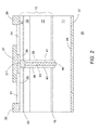
- a further distinction between transistors 10, 20 is that internal vertical connector structure 38 is formed through channel layer 19 to form a low resistance electrical connection between the source region of substrate 11 and barrier layer 21.
- the internal connector structure 38 includes a first conductor 371 formed in contact with barrier layer 21.
- First conductor 371 forms an electrical connection to the material of barrier layer 21. Typically, at least a portion of first conductor 371 abuts a portion of barrier layer 21.
- first conductor 371 is recessed within barrier layer 21.
- first conductor 371 can extend through barrier layer 21 to major surface 28 as illustrated in FIG. 2 .
- first conductor 371 forms a Schottky contact. The Schottky contact can also assist in the enhancement mode characteristics of some embodiments.
- first conductor 371 can underlie gate layer 26, but can be in other positions in other embodiments.
- First conductor 371 can be formed from polysilicon, doped polysilicon, tungsten, aluminum, or other conductor materials as known to those of skill in the art.
- Isolation layer 31 is formed to be situated on a portion of barrier layer 21 between drain electrodes 36 and the gate structure and can extend partially under a portion of gate electrode 27.
- insulator layer 31 forms a field plate that reduces the effect of high electric fields that can be formed between the drain and gate structure when transistor 20 is in operation.
- transistor 20 includes low resistance trench contact 43, which improves the operation of transistor 50.
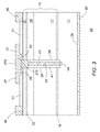
- FIG. 3 illustrates an enlarged cross-sectional view of a depletion mode semiconductor device 30 that is an alternate embodiment of transistor 20.
- Transistor 30 can be sometimes referred to as a HEMT device because of the high mobility of electrons in channel layer 19.
- Transistor 30 is similar in structure to the previously described transistor 20, with only the distinctions between the transistors 20, 30 described hereinafter.
- One distinction between transistors 20, 30 is the first conductor of internal conductor structure 38 can be extended through gate layer 26 and form an overhang 375 on dielectric layer 26.
- Gate electrode 27 is spaced apart from overhang 375 by at least 0.1 ⁇ m. In another embodiment, overhang 375 can be made out of the same metal layer as gate electrode 27.
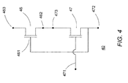
- FIG. 4 schematically illustrates a cascode circuit configuration 40 of a depletion mode HEMT device 46 and a metal oxide semiconductor field effect transistor (MOSFET) 47 in accordance with one embodiment.
- HEMT device 46 includes a gate electrode 461, a source electrode 462, and a drain electrode 463.
- MOSFET 47 includes a gate electrode 471, a source electrode 472 electrically connected to gate electrode 461 of HEMT device 46, and a drain electrode 473 electrically connected to source electrode 462 of HEMT device 46.
- depletion mode HEMT device 46 can be a 60 m ⁇ 600V HEMT and MOSFET 47 can be a 20 m ⁇ 20V silicon MOSFET.
- the threshold voltage (V th ) is determined by V th of MOSFET 47.
- V th the threshold voltage (V th ) is determined by V th of MOSFET 47.
- gate electrode 461 and source electrode 462 of HEMT device 46 are at zero volts. Because of the depletion mode characteristics, the depletion mode transistor is ON.
- gate electrode 461 of HEMT device 46 is about 10-20V below source (determined by leakage current in HEMT device 46). Because of the depletion mode characteristics, the depletion mode transistor is OFF.
- At least some of the embodiments of the HEM transistors presented herein provide an improved structure for achieving a simplified cascode stacking of a silicon MOSFET with a III-nitride depletion mode HEMT device. One attribute of this structure is that it provides enhancement mode emulation with reduced parasitic inductance between the drain of the silicon MOSFET and the source of the HEMT. Among other things, this reduces ringing effects.
- FIGS. 5A-C and 6A-C are simplified cross-sectional views of stacked MOSFET and HEMT devices and top views of the stacked devices on example lead frame structures to illustrate embodiments of cascode configuration 40.
- FIG. 5A illustrates a MOSFET 47 stacked onto a depletion mode HEMT device 46 in accordance with a first embodiment.
- HEMT device 46 is a drain down configuration and can be, for example, similar to transistor 10.
- HEMT device 46 includes drain electrode 463, which is in electrical communication with vertical internal conductor structures 465 described previously.
- source electrode 462 is separated from gate electrode 461 by insulative layer 31 described previously.
- MOSFET 47 is attached to source electrode 462 using a conductive attach structure 480, which can be, for example, a conductive solder or epoxy or other materials.
- drain electrode 473 of MOSFET 47 is attached to source electrode 462 of HEMT device 46. It is understood that some of the details of HEMT device 46 discussed previously in conjunction with transistor 10 may not be shown in FIG 5A to simply the illustration.
- FIG. 5B is a top view of a packaged semiconductor device 50 at an intermediate stage of fabrication.
- device 50 has a lead frame 52 that includes a die pad 54 and a plurality of leads 56. It is understood that device 50 can use other types of package substrates.
- drain electrode 463 of HEMT device 46 is attached with a conductive material (not shown) to die pad 54.
- Gate electrode 461 is electrically connected to one of the leads 56 configured as a gate lead 561.
- gate electrode 461 is connected to gate lead 561 with a conductive wire 58.
- One of leads 52 is configured as a drain lead 563 and in some embodiments is directly connected to die pad 54 as illustrated in FIG. 5B .
- Element 462 is the source electrode, which is sized and configured to facilitate the placement of MOSFET 47 in contact with it.
- FIG. 5C is a top view of packaged semiconductor device 50 after additional processing that includes attaching MOSFET 47 to source electrode 462 of HEMT device 46 with conductive attach structure 480 (illustrated in FIG. 5A ).
- Source electrode 472 of MOSFET 47 is electrically connected to gate lead 561 with, for example, another conductive wire 58.
- Gate electrode 471 of MOSFET 47 is electrically connected to another lead 56 configured as another gate lead 562 with, for example, a further conductive wire 58.
- Packaged semiconductor device 50 can then be encapsulated with a molded resin material 59 to protect the structure.
- Packaged semiconductor device 50 is an embodiment of a cascode transistor configuration 40 illustrated in FIG. 4 that is facilitated by HEMT device 46 having a drain down configuration in accordance with at least one of the present embodiments.
- FIG. 6A illustrates a MOSFET 47 stacked onto a depletion mode HEMT device 46 in accordance with another embodiment.
- HEMT device 46 is a source down configuration and can be, for example, similar to transistor 30.
- HEMT device 46 includes source electrode 462, which is in electrical communication with vertical internal conductor structures 465 described previously.
- drain electrode 463 is separated from gate electrode 461 by insulative layer 31 described previously.
- MOSFET 47 is attached to source electrode 462 using a conductive attach structure 480, which can be, for example, a conductive solder or epoxy or other materials.
- drain electrode 473 of MOSFET 47 is attached to source electrode 462 of HEMT device 46. It is understood that some of the details of HEMT device 46 discussed previously in conjunction with transistor 30 may not be shown in FIG 6A to simply the illustration.
- FIG. 6B is a top view of a packaged semiconductor device 60 at an intermediate stage of fabrication.
- device 60 has a lead frame 62 with a die pad 64 and plurality of leads 66. It is understood that device 60 can use other types of package substrates.
- drain electrode 463 of HEMT device 46 is attached with a conductive material (not shown) to die pad 64 and gate electrode 461 is attached with a conductive material to one leads 66 configured as a gate lead 661.
- HEMT device 46 can be attached with a conductive solder, a conductive epoxy or similar material.
- the outline of HEMT device 46 is shown as a dashed line to illustrate the direct attachment of gate electrode 461 and drain electrode directly lead frame 62.
- One of leads 66 is configured as a drain lead 663 and in some embodiments is directly connected to die pad 64 as illustrated in FIG. 6B .
- FIG. 6C is a top view of packaged semiconductor device 60 after additional processing that includes attaching MOSFET 47 to source electrode 462 of HEMT device 46 with conductive attach structure 480 (not shown).
- Source electrode 472 of MOSFET 47 is electrically connected to gate lead 661 with, for example, another conductive wire 58.
- Gate electrode 471 of MOSFET 47 is electrically connected to another lead 66 configured as another gate lead 662 with, for example, a further conductive wire 58.
- Packaged semiconductor device 60 can then be encapsulated with a molded resin material 68 to protect the structure.
- Packaged semiconductor device 60 is an embodiment of a cascode transistor configuration 40 illustrated in FIG. 4 that is facilitated by HEMT device 46 having a source down configuration in accordance with the present embodiments.
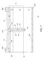
- FIG. 7 illustrates an enlarged cross-sectional view of an embodiment of a Schottky diode 70.
- Diode 70 is similar in structure to transistor 20 ( FIG. 2 ), with only the distinctions between the transistor 20 and diode 70 described hereinafter.
- One distinction between transistor 20 and diode 70 is gate layer 26 and gate electrode 27 are omitted.
- another insulative layer 310 overlies first conductor 371 of the internal conductor structure. Insulative layer 310 can be a similar material to insulative layer 31. In some embodiments, insulative layer 310 can be silicon nitride.
- electrodes 360 are configured as anode electrodes for diode 70 and electrode 370 is configured as a cathode electrode for diode 70.
- Electrodes 360 and 370 can be similar materials as described previously for electrodes 36 and 37. Electrode 360 makes a Schottky contact to 2DEG region 22, whereas electrode 371 makes an ohmic contact to 2DEG region 22.
- internal conductor structure 38 provides a vertical conduction path between the anodes and cathode of diode 70. This configuration is referred to as "cathode-down”. In yet another embodiment, referred to as "anode-down", electrode 360 makes an ohmic contact to 2DEG region 22, whereas electrode 371 makes a Schottky contact to 2DEG region 22.
- Internal conductor structure 38 provides a vertical conduction path between the anodes and cathode of diode 70
- FIG. 8 illustrates an enlarged cross-sectional view of an embodiment of a multi-transistor device 90 that includes a depletion mode HEMT device 910 and a silicon MOSFET 920 formed together in a cascode circuit configuration monolithically on one semiconductor substrate resulting in a monolithically integrated semiconductor device.
- the one semiconductor substrate includes substrate 11 having heterostructure 13 or substrate 11 with layer 12 and having heterostructure 13 as described previously.
- Device 90 includes a depletion mode HEMT transistor 910 that can be configured similarly to transistor 30.
- substrate 11 of device 90 can have a different doping concentration, for example a lower dopant concentration, than that of substrate 11 of transistor 30.
- Substrate 11 forms the source of HEMT device 910 and a drain of HEMT device 910 is formed on surface 28 of device 90 similarly to transistor 30.
- Gate layer 26 underlies at least one portion of gate electrode or conductor 27 of HEMT device 910. The drain of the HEMT is contact 36.
- region 920 of device 90 the 2DEG region 22 is destroyed, for example, by ion implantation with nitrogen, argon, iron, or similar methods as known to those of ordinary skill in the art.
- region 910 (HEMT device) of device 90 the 2DEG region 22 is maintained.
- a first internal conductor structure 911 forms a low resistance connection to and between 2DEG region 22 (and hence the drain region of MOSFET device 920) and substrate 11.
- first internal conductor structure 911 is similar to internal conductor structure 38 and includes a trench 39 extending from major surface 28 into substrate 11. Similar to transistor 30, trench 39 is lined with insulating layer 41 and further includes a conductive trench contact 43 configured to provide an ohmic contact to substrate 11.
- first internal conductor structure 911 is electrically connected to 2DEG region 22 through first conductor 372, which forms an electrical connection to trench contact 43.
- Conductor 372 is isolated from gate electrode 27 through insulating layer 31.
- a second internal conductor structure 913 forms a low resistance connection to and between gate electrode 27 and substrate 11.
- second internal conductor structure 913 includes a trench 39 extending from major surface 28 into substrate 11. Similar to transistor 30, trench 39 is lined with insulating layer 41 and further includes a conductive trench contact 43 configured to provide an ohmic contact to substrate 11.
- second internal conductor structure 913 is electrically connected to a source electrode 472 with a second conductor 373, which extends through the underlying insulative layer 31 and forms an electrical connection to trench contact 43. In this configuration, second internal conductor structure 913 forms a source region with a portion of substrate 11 for MOSFET 920.
- first internal conductor structure 911 forms a drain of MOSFET 920 with another portion of substrate 11. Additionally, first internal conductor structure 911 is configured to function as at least a portion of the source of HEMT device 910. Thus, in accordance with the present embodiment, the source of HEMT device 910 and the drain of MOSFET 920 are connected together as illustrated in FIG. 4 .
- Second internal conductor structure 913 forms an electrical connection between the source of MOSFET 920 and a source conductor electrode 472 formed on the surface of device 90.
- source electrode conductor 472 also connects to gate electrode 27 of HEMT device 910. This forms an electrical connection between the HEMT gate and the MOSFET source as illustrated in FIG. 4 .
- a doped region 921 is formed in substrate 11 in a region between the source and drain of MOSFET 920 to form a channel region of MOSFET 920.
- Doped region 921 has a doping type that has opposite conductivity to that of substrate 11.
- doped region 921 is p-type and has a dopant concentration configured to form a channel under a selected gate bias.
- An internal gate structure 916 of MOSFET 920 is formed adjoining doped region 921.
- internal gate structure 916 has a similar structure to first and second internal conductor structures 911 and 913.
- internal gate structure 916 includes a trench 39 lined with insulating layer 41 and having a trench conductor 43.
- internal gate structure 916 includes gate dielectric layer 926 separating trench conductor 43 from doped region 921.
- gate dielectric layer 926 is silicon oxide or other gate materials used in MOSFET devices.
- gate dielectric layer 926 is thinner than insulating layer 41.
- a portion 81 of insulating layer 31 on major surface 28 on the surface near the HEMT gate is extended to cover another end of the trench conductor 43 in internal gate structure 916.
- electrical contact is made to trench conductor 43 in internal gate structure 916 in another portion of device 90 (not shown).
- FIG. 9 illustrates an enlarged cross-sectional view of an embodiment of a multi-transistor device 100 that is an alternate embodiment of device 90 illustrated in FIG. 8 .
- Device 100 is similar to device 90 but has a different conductivity type of MOSFET 930.
- substrate 11 in device 100 includes a p-type substrate instead of the N-type substrate of device 90.
- a portion of substrate 11 below internal gate structure 916 functions as the channel region of the MOSFET.
- Device 100 also includes a first doped region 927 of an opposite conductivity type (opposite to the substrate type, for example, n-type) formed in the substrate to function as the source region of MOSFET 930.
- Another doped region 923 of the opposite conductivity type to substrate 11 is formed to function as the drain of MOSFET 930 and the source of HEMT device 910.
- the gate of the MOSFET is formed as a gate structure similar to the gate structure of device 90 except that the gate structure adjoins a channel region of the substrate instead of a channel region formed by a doped region formed in the substrate.
- first conductor 372 is isolated from gate electrode 27 by insulative layer 31 in first internal conductor structure 911.
- a method of forming a semiconductor device can comprise providing a base substrate of a first semiconductor material (for example, element 11) wherein the base substrate defines a first current carrying electrode of the semiconductor device; forming III-nitride channel layer (for example, element 19) on the base substrate; forming a III-nitride barrier layer (for example, element 21) on the channel layer; forming a second current carrying electrode of the semiconductor device in the barrier layer; forming a gate (for example, element 27) of the semiconductor device overlying a portion of the barrier layer and spaced apart from the second current carrying electrode; and forming a first internal conductor structure (for example, element 38) extending from the barrier layer through the channel layer to the base substrate wherein the internal connector structure forms a low resistance vertical electrical current path from the base substrate to the barrier layer.
- the method can include forming the internal conductor structure to electrically connect to the base substrate and to the barrier layer.
- a further embodiment of the method can include forming a first conductor within the barrier layer and forming a second conductor extending from the first conductor to the base substrate and forming an insulator between the second conductor and the channel layer.
- the method can include forming a Schottky barrier connection between the first conductor and the barrier layer.
- the method can include forming the internal conductor structure to electrically connect to the base substrate and to a major surface of the barrier layer.
- the method can include forming a first doped region of a first conductivity type in the base substrate and spaced apart from the first internal conductor structure wherein the first conductivity type is opposite to a conductivity type of the base substrate; forming a gate conductor of a MOS transistor overlying the first doped region wherein a portion of the first doped region forms a channel region of the MOS transistor; forming a second internal conductor structure adjacent to but spaced apart from the first doped region, the second internal conductor structure extending from the barrier layer through the channel layer to the base substrate wherein the internal connector structure forms a low resistance electrical current path.
- Another embodiment of the method can include forming a first current carrying electrode of the MOS transistor as a portion of the base substrate underlying the first internal conductor structure.
- the method can also forming an electrical path between the gate and the second internal conductor structure to form a low resistance electrical connection from the gate to the base substrate wherein a portion of the base substrate underlying the second internal conductor structure forms a first current carrying electrode of the MOS transistor.
- Another embodiment of the method can include forming a first doped region of a first conductivity type in the base substrate and abutting the first internal conductor structure wherein the first conductivity type is opposite to a conductivity type of the base substrate and wherein the first doped region forms a first current carrying electrode of an MOS transistor; forming a second doped region of the first conductivity type in the base substrate and spaced apart from the first doped region wherein the second doped region forms a second current carrying electrode of the MOS transistor; forming a gate conductor of the MOS transistor overlying a portion of the base substrate that is between the first and second doped regions wherein the portion of the base substrate forms a channel region of an MOS transistor; forming a second internal conductor structure extending from the barrier layer through the channel layer to the second doped region wherein the internal connector structure forms a low resistance electrical current path.
- the method can also include forming an electrical path between the gate and the second internal conductor structure to form a low resistance electrical connection from the gate to the second current carrying electrode of the MOS transistor.
- a semiconductor device can comprise a semiconductor substrate (for example, element 11) of a first conductivity type, wherein the semiconductor substrate provides a first current carrying electrode of the semiconductor device; a plurality of III-nitride layers (for example, elements 16, 17, 19, 21) on the semiconductor substrate to provide an HEM structure; and an internal conductor structure (for example, element 38) extending from a major surface (for example, element 28) of the HEM structure to the semiconductor substrate providing a vertical current path from the semiconductor substrate to the HEM structure.
- Another embodiment can include an epitaxial layer between the conductive substrate and the plurality of III-nitride layers, wherein the epitaxial layer is of the first conductivity type and has a lower dopant concentration than the semiconductor substrate.
- the internal conductor structure includes a dielectric liner along a trench sidewall, which has an opening at the bottom of the trench; a trench filling, using a highly conductive layer, making contact to the conductive substrate and to a 2DEG region of the HEM device; and a first current carrying contact adjoining a back surface of the semiconductor substrate and in electrical communication with the trench filling.
- the plurality of III-nitride layers includes a GaN channel layer and an AlGaN barrier layer on the GaN channel layer to provide the 2DEG region.
- the semiconductor device can further include a second current carrying contact in the AlGaN barrier layer; and a gate structure overlying a portion of the AlGaN barrier layer and spaced apart from the second current carrying electrode, and wherein the internal connector structure forms a low resistance electrical current path from the semiconductor substrate to the AlGaN barrier layer.
- a semiconductor device can a base substrate (for example, element 11) of a first semiconductor material wherein the base substrate forms a first current carrying electrode of the semiconductor device; a heterostructure (for example, element 13) comprising a III-nitride channel layer (for example, element 19) over the base substrate and a III-nitride barrier layer (for example, element 21) over the channel layer; a second current carrying electrode of the semiconductor device in the barrier layer (for example, element 36, 37); a gate (for example, element 27) of the semiconductor device overlying a portion of the barrier layer and spaced apart from the second current carrying electrode; and a first internal conductor structure (for example, element 38) extending from the barrier layer through the channel to the base substrate wherein the internal connector structure forms a low resistance electrical current path from the base substrate to the barrier layer.
- a base substrate for example, element 11
- a heterostructure for example, element 13
- III-nitride channel layer for example, element 19
- a III-nitride barrier layer
- the first internal conductor structure electrically connects to the base substrate and to the barrier layer.
- the first internal conductor structure is within the barrier layer and further comprises a second conductor extending from the first conductor to the base substrate, and wherein the second conductor is insulated from the channel layer.
- the heterostructure comprises an AlGaN buffer layer on the base substrate; a GaN channel layer on the AlGaN buffer region; and an AlGaN barrier layer on the GaN channel layer.
- the semiconductor device further comprises a first doped region of a first conductivity type in the base substrate and spaced apart from the first internal conductor structure wherein the first conductivity type is opposite to a conductivity type of the base substrate; a gate conductor of an MOS transistor overlying the first doped region wherein a portion of the first doped region forms a channel region of the MOS transistor; and a second internal conductor structure adjacent to but spaced apart from the first doped region, the second internal conductor structure extending from the barrier layer through the channel layer to the base substrate, wherein the internal connector structure forms a low resistance electrical current path.
- the semiconductor device further comprises a first doped region of a first conductivity type in the base substrate and abutting the first internal conductor structure wherein the first conductivity type is opposite to a conductivity type of the base substrate and wherein the first doped region forms a first current carrying electrode of an MOS transistor; a second doped region of the first conductivity type in the base substrate and spaced apart from the first doped region wherein the second doped region forms a second current carrying electrode of the MOS transistor; a gate conductor of the MOS transistor overlying a portion of the base substrate that is between the first and second doped regions wherein the portion of the base substrate forms a channel region of an MOS transistor; and a second internal conductor structure extending from the barrier layer through the channel layer to the second doped region wherein the internal connector structure forms a low resistance electrical current path.
- an enhancement region is included in the base substrate adjoining the second internal conductor.
- the enhancement region is a doped region.
- the enhancement region is a silicide region.
- a highly doped base semiconductor substrate provides one current carrying electrode for the HEM device.
- a heterostructure is provided on the base semiconductor substrate and includes a III-nitride channel layer and a III-nitride barrier layer on the channel layer.
- a second current carrying electrode is situated in proximity to the barrier layer and, in some embodiments, a gate structure is provided in spaced relationship with the barrier layer.
- the structure includes at least one internal conductor structure that provides a vertical current path between the second current carrying electrode and the base substrate.
- the method and structure provide for the routing source and gate conductive lines on the top surface of the structure with the drain conductive layer on the back surface of the die.
- both the source and gate terminals are biased at low voltage, which puts a lower stress on inter-metal dielectric structures. This lower stress reduces electro-migration issues.
- the structure also provides for semiconductor chip area savings of at least 30% because bonding to the source and gate terminals can be done over the active area of the device. Additionally, the configuration facilitates the assembly of the HEM devices with other devices such as silicon MOSFET devices, which reduces parasitic inductances and resistances.
- inventive aspects can lie in less than all features of a single foregoing disclosed embodiment.
- inventive aspects can lie in less than all features of a single foregoing disclosed embodiment.
- the hereinafter expressed claims are hereby expressly incorporated into this Detailed Description of the Drawings, with each claim standing on its own as a separate embodiment of an invention.
- some embodiments described herein include some but not other features included in other embodiments, combinations of features of different embodiments are meant to be within the scope of the invention, and form different embodiments, as would be understood by those skilled in the art.
Landscapes
- Junction Field-Effect Transistors (AREA)
Applications Claiming Priority (2)
| Application Number | Priority Date | Filing Date | Title |
|---|---|---|---|
| US201361786596P | 2013-03-15 | 2013-03-15 | |
| US14/182,508 US9269789B2 (en) | 2013-03-15 | 2014-02-18 | Method of forming a high electron mobility semiconductor device and structure therefor |
Publications (2)
| Publication Number | Publication Date |
|---|---|
| EP2779246A2 true EP2779246A2 (fr) | 2014-09-17 |
| EP2779246A3 EP2779246A3 (fr) | 2017-11-29 |
Family
ID=50241309
Family Applications (1)
| Application Number | Title | Priority Date | Filing Date |
|---|---|---|---|
| EP14159610.6A Ceased EP2779246A3 (fr) | 2013-03-15 | 2014-03-13 | Procédé de formation d'un dispositif semi-conducteur à haute mobilité d'électrons et structure associée |
Country Status (3)
| Country | Link |
|---|---|
| US (2) | US9269789B2 (fr) |
| EP (1) | EP2779246A3 (fr) |
| CN (1) | CN104319238B (fr) |
Cited By (5)
| Publication number | Priority date | Publication date | Assignee | Title |
|---|---|---|---|---|
| EP3331027A3 (fr) * | 2016-12-02 | 2018-10-24 | Vishay-Siliconix | Transistor à mobilité électronique élevée et à interconnexion enterrée |
| US10224426B2 (en) | 2016-12-02 | 2019-03-05 | Vishay-Siliconix | High-electron-mobility transistor devices |
| EP3644361A4 (fr) * | 2017-06-19 | 2020-06-17 | Shindengen Electric Manufacturing Co., Ltd. | Dispositif à semi-conducteur |
| US10693288B2 (en) | 2018-06-26 | 2020-06-23 | Vishay SIliconix, LLC | Protection circuits with negative gate swing capability |
| US10833063B2 (en) | 2018-07-25 | 2020-11-10 | Vishay SIliconix, LLC | High electron mobility transistor ESD protection structures |
Families Citing this family (27)
| Publication number | Priority date | Publication date | Assignee | Title |
|---|---|---|---|---|
| IT1398204B1 (it) | 2010-02-16 | 2013-02-14 | St Microelectronics Srl | Sistema e metodo per eseguire il test elettrico di vie passanti nel silicio (tsv - through silicon vias). |
| US9368584B2 (en) | 2013-07-09 | 2016-06-14 | Vishay General Semiconductor Llc | Gallium nitride power semiconductor device having a vertical structure |
| US10553633B2 (en) * | 2014-05-30 | 2020-02-04 | Klaus Y.J. Hsu | Phototransistor with body-strapped base |
| CN104332498B (zh) * | 2014-09-01 | 2018-01-05 | 苏州捷芯威半导体有限公司 | 一种斜场板功率器件及斜场板功率器件的制备方法 |
| US9640620B2 (en) * | 2014-11-03 | 2017-05-02 | Texas Instruments Incorporated | High power transistor with oxide gate barriers |
| JP6261553B2 (ja) * | 2015-11-27 | 2018-01-17 | 株式会社豊田中央研究所 | 窒化物半導体装置及びその製造方法 |
| JP6817796B2 (ja) * | 2016-11-28 | 2021-01-20 | ルネサスエレクトロニクス株式会社 | 半導体装置の製造方法 |
| US9966318B1 (en) * | 2017-01-31 | 2018-05-08 | Stmicroelectronics S.R.L. | System for electrical testing of through silicon vias (TSVs) |
| CN109148606B (zh) * | 2017-06-28 | 2022-04-12 | 联华电子股份有限公司 | 高压元件 |
| CN107482059B (zh) * | 2017-08-02 | 2020-01-17 | 电子科技大学 | 一种GaN异质结纵向逆导场效应管 |
| TWI728165B (zh) * | 2017-08-08 | 2021-05-21 | 晶元光電股份有限公司 | 三族氮化物高速電子遷移率場效應電晶體元件 |
| CN111199958A (zh) * | 2018-11-16 | 2020-05-26 | 苏州东微半导体有限公司 | 半导体功率器件 |
| CN111816701B (zh) * | 2019-04-12 | 2024-12-27 | 广东致能科技有限公司 | 一种半导体器件及其制造方法 |
| US11031281B2 (en) * | 2019-06-04 | 2021-06-08 | Globalfoundries Singapore Pte. Ltd. | Semiconductor devices and methods of fabricating a deep trench isolation structure |
| US11038048B2 (en) | 2019-10-01 | 2021-06-15 | Taiwan Semiconductor Manufacturing Company, Ltd. | Gallium nitride-on-silicon devices |
| CN113394209B (zh) * | 2020-03-12 | 2023-01-13 | 青岛聚能创芯微电子有限公司 | 氮化镓器件封装结构 |
| FR3111738B1 (fr) * | 2020-06-19 | 2022-08-05 | Commissariat Energie Atomique | Dispositif micro-électronique à substrat isolé, et procédé de fabrication associé |
| WO2021257965A1 (fr) * | 2020-06-19 | 2021-12-23 | Macom Technology Solutions Holdings, Inc. | Suppression d'ondes acoustiques parasites dans des dispositifs à circuit intégré |
| JP7476062B2 (ja) * | 2020-09-15 | 2024-04-30 | 株式会社東芝 | 半導体装置 |
| WO2022174400A1 (fr) | 2021-02-19 | 2022-08-25 | Innoscience (Suzhou) Technology Co., Ltd. | Dispositif à semi-conducteur et son procédé de fabrication |
| CN114270533B (zh) | 2021-02-19 | 2024-01-02 | 英诺赛科(苏州)科技有限公司 | 半导体器件及其制造方法 |
| WO2022217538A1 (fr) * | 2021-04-15 | 2022-10-20 | 苏州晶湛半导体有限公司 | Structure semi-conductrice et son procédé de préparation |
| US20240055314A1 (en) * | 2022-08-09 | 2024-02-15 | Nxp B.V. | Transistor heat dissipation structure |
| CN115799330A (zh) * | 2022-11-11 | 2023-03-14 | 深圳天狼芯半导体有限公司 | 耐高压hemt器件及其制备方法 |
| CN120076368A (zh) * | 2023-11-16 | 2025-05-30 | 镓合半导体(上海)有限公司 | 一种高耐压hemt器件、及其驱动方法 |
| CN118486719A (zh) * | 2024-05-31 | 2024-08-13 | 深圳平湖实验室 | 一种叠层结构的级联型氮化镓功率器件及其制备方法 |
| CN119092539A (zh) * | 2024-06-13 | 2024-12-06 | 润新微电子(大连)有限公司 | 一种耗尽型GaN器件的制备方法 |
Family Cites Families (6)
| Publication number | Priority date | Publication date | Assignee | Title |
|---|---|---|---|---|
| JP4645313B2 (ja) * | 2005-06-14 | 2011-03-09 | 富士電機システムズ株式会社 | 半導体装置 |
| JP2007165446A (ja) * | 2005-12-12 | 2007-06-28 | Oki Electric Ind Co Ltd | 半導体素子のオーミックコンタクト構造 |
| US7821034B2 (en) * | 2006-01-09 | 2010-10-26 | International Rectifier Corporation | Integrated III-nitride devices |
| DE102009018054B4 (de) * | 2009-04-21 | 2018-11-29 | Infineon Technologies Austria Ag | Lateraler HEMT und Verfahren zur Herstellung eines lateralen HEMT |
| US9219058B2 (en) | 2010-03-01 | 2015-12-22 | Infineon Technologies Americas Corp. | Efficient high voltage switching circuits and monolithic integration of same |
| WO2012082840A1 (fr) * | 2010-12-15 | 2012-06-21 | Efficient Power Conversion Corporation | Dispositifs à semi-conducteurs à isolation de surface arrière |
-
2014
- 2014-02-18 US US14/182,508 patent/US9269789B2/en active Active
- 2014-03-13 EP EP14159610.6A patent/EP2779246A3/fr not_active Ceased
- 2014-03-14 CN CN201410095344.5A patent/CN104319238B/zh active Active
-
2016
- 2016-01-06 US US14/989,370 patent/US9543291B2/en active Active
Non-Patent Citations (1)
| Title |
|---|
| None |
Cited By (9)
| Publication number | Priority date | Publication date | Assignee | Title |
|---|---|---|---|---|
| EP3331027A3 (fr) * | 2016-12-02 | 2018-10-24 | Vishay-Siliconix | Transistor à mobilité électronique élevée et à interconnexion enterrée |
| US10224426B2 (en) | 2016-12-02 | 2019-03-05 | Vishay-Siliconix | High-electron-mobility transistor devices |
| US10381473B2 (en) | 2016-12-02 | 2019-08-13 | Vishay-Siliconix | High-electron-mobility transistor with buried interconnect |
| US10651303B2 (en) | 2016-12-02 | 2020-05-12 | Vishay SIliconix, LLC | High-electron-mobility transistor devices |
| US10665711B2 (en) | 2016-12-02 | 2020-05-26 | Vishay SIliconix, LLC | High-electron-mobility transistor with buried interconnect |
| EP4148806A1 (fr) | 2016-12-02 | 2023-03-15 | Vishay-Siliconix | Transistor à haute mobilité électronique avec interconnexion enterrée |
| EP3644361A4 (fr) * | 2017-06-19 | 2020-06-17 | Shindengen Electric Manufacturing Co., Ltd. | Dispositif à semi-conducteur |
| US10693288B2 (en) | 2018-06-26 | 2020-06-23 | Vishay SIliconix, LLC | Protection circuits with negative gate swing capability |
| US10833063B2 (en) | 2018-07-25 | 2020-11-10 | Vishay SIliconix, LLC | High electron mobility transistor ESD protection structures |
Also Published As
| Publication number | Publication date |
|---|---|
| US9269789B2 (en) | 2016-02-23 |
| CN104319238A (zh) | 2015-01-28 |
| US20140264453A1 (en) | 2014-09-18 |
| CN104319238B (zh) | 2018-12-18 |
| US20160118377A1 (en) | 2016-04-28 |
| US9543291B2 (en) | 2017-01-10 |
| EP2779246A3 (fr) | 2017-11-29 |
Similar Documents
| Publication | Publication Date | Title |
|---|---|---|
| US9543291B2 (en) | Method of forming a high electron mobility semiconductor device and structure therefor | |
| US10707203B2 (en) | Cascode semiconductor device structure and method therefor | |
| US8981380B2 (en) | Monolithic integration of silicon and group III-V devices | |
| EP2793255B1 (fr) | Procédé de fabrication d'un dispositif semi-conducteur comprenant une diode schottky et un transistor à haute mobilité d'électrons | |
| US7838907B2 (en) | Semiconductor device and power conversion device using the same | |
| US9276097B2 (en) | Gate overvoltage protection for compound semiconductor transistors | |
| US8941217B2 (en) | Semiconductor device having a through contact | |
| JP2005093864A (ja) | 電力用半導体装置 | |
| US8723238B1 (en) | Method of forming a transistor and structure therefor | |
| KR20180063837A (ko) | 상호 접속부가 매립된 고 전자 이동도 트랜지스터 | |
| US20160086939A1 (en) | Semiconductor device | |
| US20240063219A1 (en) | Integrated depletion and enhancement mode gallium nitride high-electron mobility transistors | |
| TW201939616A (zh) | 橫向擴散金屬氧化物半導體(ldmos)電晶體及其製造方法 | |
| US12581683B2 (en) | P-type gate HEMT device | |
| US11251263B2 (en) | Electronic device including a semiconductor body or an isolation structure within a trench | |
| US20250301778A1 (en) | Semiconductor devices in integrated circuit having different threshold voltages | |
| US9287377B2 (en) | Semiconductor device and manufacturing method | |
| CN205140988U (zh) | 半导体器件 | |
| US20250301680A1 (en) | Semiconductor devices in integrated circuit having different threshold voltages |
Legal Events
| Date | Code | Title | Description |
|---|---|---|---|
| 17P | Request for examination filed |
Effective date: 20140313 |
|
| AK | Designated contracting states |
Kind code of ref document: A2 Designated state(s): AL AT BE BG CH CY CZ DE DK EE ES FI FR GB GR HR HU IE IS IT LI LT LU LV MC MK MT NL NO PL PT RO RS SE SI SK SM TR |
|
| AX | Request for extension of the european patent |
Extension state: BA ME |
|
| PUAI | Public reference made under article 153(3) epc to a published international application that has entered the european phase |
Free format text: ORIGINAL CODE: 0009012 |
|
| PUAL | Search report despatched |
Free format text: ORIGINAL CODE: 0009013 |
|
| AK | Designated contracting states |
Kind code of ref document: A3 Designated state(s): AL AT BE BG CH CY CZ DE DK EE ES FI FR GB GR HR HU IE IS IT LI LT LU LV MC MK MT NL NO PL PT RO RS SE SI SK SM TR |
|
| AX | Request for extension of the european patent |
Extension state: BA ME |
|
| RIC1 | Information provided on ipc code assigned before grant |
Ipc: H01L 23/495 20060101ALI20171020BHEP Ipc: H01L 29/417 20060101ALI20171020BHEP Ipc: H01L 29/41 20060101ALI20171020BHEP Ipc: H01L 29/20 20060101ALN20171020BHEP Ipc: H01L 29/205 20060101ALN20171020BHEP Ipc: H01L 29/872 20060101ALI20171020BHEP Ipc: H01L 21/8252 20060101ALI20171020BHEP Ipc: H01L 27/06 20060101ALI20171020BHEP Ipc: H01L 29/10 20060101ALN20171020BHEP Ipc: H01L 21/336 20060101ALI20171020BHEP Ipc: H01L 29/423 20060101ALN20171020BHEP Ipc: H01L 29/778 20060101AFI20171020BHEP |
|
| STAA | Information on the status of an ep patent application or granted ep patent |
Free format text: STATUS: REQUEST FOR EXAMINATION WAS MADE |
|
| R17P | Request for examination filed (corrected) |
Effective date: 20180529 |
|
| RBV | Designated contracting states (corrected) |
Designated state(s): AL AT BE BG CH CY CZ DE DK EE ES FI FR GB GR HR HU IE IS IT LI LT LU LV MC MK MT NL NO PL PT RO RS SE SI SK SM TR |
|
| STAA | Information on the status of an ep patent application or granted ep patent |
Free format text: STATUS: EXAMINATION IS IN PROGRESS |
|
| 17Q | First examination report despatched |
Effective date: 20200605 |
|
| STAA | Information on the status of an ep patent application or granted ep patent |
Free format text: STATUS: THE APPLICATION HAS BEEN REFUSED |
|
| 18R | Application refused |
Effective date: 20220218 |