EP2782183A1 - Reparaturvorrichtung für blattförmige batterie - Google Patents
Reparaturvorrichtung für blattförmige batterie Download PDFInfo
- Publication number
- EP2782183A1 EP2782183A1 EP20110875625 EP11875625A EP2782183A1 EP 2782183 A1 EP2782183 A1 EP 2782183A1 EP 20110875625 EP20110875625 EP 20110875625 EP 11875625 A EP11875625 A EP 11875625A EP 2782183 A1 EP2782183 A1 EP 2782183A1
- Authority
- EP
- European Patent Office
- Prior art keywords
- repair
- electrical stimulation
- sheet type
- voltage
- type cell
- Prior art date
- Legal status (The legal status is an assumption and is not a legal conclusion. Google has not performed a legal analysis and makes no representation as to the accuracy of the status listed.)
- Granted
Links
Images





Classifications
-
- H—ELECTRICITY
- H01—ELECTRIC ELEMENTS
- H01M—PROCESSES OR MEANS, e.g. BATTERIES, FOR THE DIRECT CONVERSION OF CHEMICAL ENERGY INTO ELECTRICAL ENERGY
- H01M10/00—Secondary cells; Manufacture thereof
- H01M10/42—Methods or arrangements for servicing or maintenance of secondary cells or secondary half-cells
-
- H—ELECTRICITY
- H01—ELECTRIC ELEMENTS
- H01M—PROCESSES OR MEANS, e.g. BATTERIES, FOR THE DIRECT CONVERSION OF CHEMICAL ENERGY INTO ELECTRICAL ENERGY
- H01M50/00—Constructional details or processes of manufacture of the non-active parts of electrochemical cells other than fuel cells, e.g. hybrid cells
- H01M50/50—Current conducting connections for cells or batteries
- H01M50/572—Means for preventing undesired use or discharge
-
- H—ELECTRICITY
- H01—ELECTRIC ELEMENTS
- H01M—PROCESSES OR MEANS, e.g. BATTERIES, FOR THE DIRECT CONVERSION OF CHEMICAL ENERGY INTO ELECTRICAL ENERGY
- H01M10/00—Secondary cells; Manufacture thereof
- H01M10/42—Methods or arrangements for servicing or maintenance of secondary cells or secondary half-cells
- H01M10/4242—Regeneration of electrolyte or reactants
-
- H—ELECTRICITY
- H01—ELECTRIC ELEMENTS
- H01M—PROCESSES OR MEANS, e.g. BATTERIES, FOR THE DIRECT CONVERSION OF CHEMICAL ENERGY INTO ELECTRICAL ENERGY
- H01M10/00—Secondary cells; Manufacture thereof
- H01M10/42—Methods or arrangements for servicing or maintenance of secondary cells or secondary half-cells
- H01M10/425—Structural combination with electronic components, e.g. electronic circuits integrated to the outside of the casing
-
- H—ELECTRICITY
- H01—ELECTRIC ELEMENTS
- H01M—PROCESSES OR MEANS, e.g. BATTERIES, FOR THE DIRECT CONVERSION OF CHEMICAL ENERGY INTO ELECTRICAL ENERGY
- H01M10/00—Secondary cells; Manufacture thereof
- H01M10/42—Methods or arrangements for servicing or maintenance of secondary cells or secondary half-cells
- H01M10/48—Accumulators combined with arrangements for measuring, testing or indicating the condition of cells, e.g. the level or density of the electrolyte
- H01M10/482—Accumulators combined with arrangements for measuring, testing or indicating the condition of cells, e.g. the level or density of the electrolyte for several batteries or cells simultaneously or sequentially
-
- H—ELECTRICITY
- H10—SEMICONDUCTOR DEVICES; ELECTRIC SOLID-STATE DEVICES NOT OTHERWISE PROVIDED FOR
- H10F—INORGANIC SEMICONDUCTOR DEVICES SENSITIVE TO INFRARED RADIATION, LIGHT, ELECTROMAGNETIC RADIATION OF SHORTER WAVELENGTH OR CORPUSCULAR RADIATION
- H10F71/00—Manufacture or treatment of devices covered by this subclass
-
- H—ELECTRICITY
- H10—SEMICONDUCTOR DEVICES; ELECTRIC SOLID-STATE DEVICES NOT OTHERWISE PROVIDED FOR
- H10F—INORGANIC SEMICONDUCTOR DEVICES SENSITIVE TO INFRARED RADIATION, LIGHT, ELECTROMAGNETIC RADIATION OF SHORTER WAVELENGTH OR CORPUSCULAR RADIATION
- H10F71/00—Manufacture or treatment of devices covered by this subclass
- H10F71/10—Manufacture or treatment of devices covered by this subclass the devices comprising amorphous semiconductor material
-
- Y—GENERAL TAGGING OF NEW TECHNOLOGICAL DEVELOPMENTS; GENERAL TAGGING OF CROSS-SECTIONAL TECHNOLOGIES SPANNING OVER SEVERAL SECTIONS OF THE IPC; TECHNICAL SUBJECTS COVERED BY FORMER USPC CROSS-REFERENCE ART COLLECTIONS [XRACs] AND DIGESTS
- Y02—TECHNOLOGIES OR APPLICATIONS FOR MITIGATION OR ADAPTATION AGAINST CLIMATE CHANGE
- Y02E—REDUCTION OF GREENHOUSE GAS [GHG] EMISSIONS, RELATED TO ENERGY GENERATION, TRANSMISSION OR DISTRIBUTION
- Y02E10/00—Energy generation through renewable energy sources
- Y02E10/50—Photovoltaic [PV] energy
-
- Y—GENERAL TAGGING OF NEW TECHNOLOGICAL DEVELOPMENTS; GENERAL TAGGING OF CROSS-SECTIONAL TECHNOLOGIES SPANNING OVER SEVERAL SECTIONS OF THE IPC; TECHNICAL SUBJECTS COVERED BY FORMER USPC CROSS-REFERENCE ART COLLECTIONS [XRACs] AND DIGESTS
- Y02—TECHNOLOGIES OR APPLICATIONS FOR MITIGATION OR ADAPTATION AGAINST CLIMATE CHANGE
- Y02E—REDUCTION OF GREENHOUSE GAS [GHG] EMISSIONS, RELATED TO ENERGY GENERATION, TRANSMISSION OR DISTRIBUTION
- Y02E60/00—Enabling technologies; Technologies with a potential or indirect contribution to GHG emissions mitigation
- Y02E60/10—Energy storage using batteries
-
- Y—GENERAL TAGGING OF NEW TECHNOLOGICAL DEVELOPMENTS; GENERAL TAGGING OF CROSS-SECTIONAL TECHNOLOGIES SPANNING OVER SEVERAL SECTIONS OF THE IPC; TECHNICAL SUBJECTS COVERED BY FORMER USPC CROSS-REFERENCE ART COLLECTIONS [XRACs] AND DIGESTS
- Y02—TECHNOLOGIES OR APPLICATIONS FOR MITIGATION OR ADAPTATION AGAINST CLIMATE CHANGE
- Y02P—CLIMATE CHANGE MITIGATION TECHNOLOGIES IN THE PRODUCTION OR PROCESSING OF GOODS
- Y02P70/00—Climate change mitigation technologies in the production process for final industrial or consumer products
- Y02P70/50—Manufacturing or production processes characterised by the final manufactured product
-
- Y—GENERAL TAGGING OF NEW TECHNOLOGICAL DEVELOPMENTS; GENERAL TAGGING OF CROSS-SECTIONAL TECHNOLOGIES SPANNING OVER SEVERAL SECTIONS OF THE IPC; TECHNICAL SUBJECTS COVERED BY FORMER USPC CROSS-REFERENCE ART COLLECTIONS [XRACs] AND DIGESTS
- Y10—TECHNICAL SUBJECTS COVERED BY FORMER USPC
- Y10T—TECHNICAL SUBJECTS COVERED BY FORMER US CLASSIFICATION
- Y10T29/00—Metal working
- Y10T29/53—Means to assemble or disassemble
- Y10T29/5313—Means to assemble electrical device
- Y10T29/53135—Storage cell or battery
Definitions
- the present invention relates to a repair apparatus of a sheet type cell, which can be applied to repair of a cell based on an operation principal of forming a new energy level in a band gap and capturing an electron by utilizing a photoexcited structural change of a metal oxide (hereinafter referred to as a quantum cell), for example.
- a repair apparatus of a sheet type cell which can be applied to repair of a cell based on an operation principal of forming a new energy level in a band gap and capturing an electron by utilizing a photoexcited structural change of a metal oxide (hereinafter referred to as a quantum cell), for example.
- a quantum cell a photoexcited structural change of a metal oxide
- NiMH nickel-metal hydride cells
- LIB lithium ion secondary cells
- solar cells are known as plate type devices.
- the solar cell is not a cell, but has semiconductor characteristics, and the electrical repair of defects thereof is implemented (see Patent Document 1 to Patent Document 3).
- the suggested repair of a solar cell is performed by electrical stimulation with a voltage source brought into contact with comb-shaped electrodes of the solar cell. The voltage is applied between adjacent comb-shaped electrodes so that a reverse bias voltage is applied to PN junctions of the solar cell.
- the invention is made in view of the above-described circumstances, and aims at providing a repair apparatus of a sheet type cell that is capable of appropriately repairing and detoxifying defects of a sheet type cell having semiconductor characteristics.
- the present invention provides a repair apparatus of a sheet type cell for repairing the sheet type cell in which a storage layer is sandwiched by layers of a positive electrode and a negative electrode and at least the storage layer has semiconductor characteristics, the repair apparatus including (1) an electrical stimulation source that applies electrical stimulation between the positive electrode and the negative electrode, (2) an electrical characteristic measurement means that measures electrical characteristics of the sheet type cell when the electrical stimulation is applied, and (3) a control means that specifies a value of the electrical stimulation by the electrical stimulation source while considering measured electrical characteristics.
- a sheet type cell having semiconductor characteristics is suitable for an object to be repaired.
- the repair apparatus according to the embodiment is described supposing that a quantum cell is the object to be repaired, for example.
- Fig. 1 is an explanatory view showing a layered structure of a sheet type cell which is an object to be repaired.
- a sheet type cell to be repaired is not limited to the one which is implemented as a secondary cell, but may be the one which is implemented as a primary cell.
- the sheet type cell is a secondary cell.
- any sheet type (parallel plate type) cell is suitable for an object to be repaired.
- a solid state sheet type cell 1 in which a storage layer 2 having a function as an electricity storage unit is sandwiched between layers of a positive electrode 4 and a negative electrode 3 may be an object to be repaired.
- Fig. 1 shows the state where the sheet type cell 1 is attached on a substrate 5, and a positive electrode terminal 7 and a negative electrode terminal 6 are attached on the positive electrode 4 and the negative electrode 3, respectively.
- the above-described quantum cell in which a photoexcited structural change is used may be an object to be repaired.
- the storage layer in the quantum cell is referred to as a charging layer, in view of its characteristics.
- the charging layer stores electrons with a charging operation, releases the charged electrons with a discharging operation, and keeps the electrons (storage of electricity) in a state without charging/discharging.
- the charging layer is formed by applying a technology of photoexcited structural change.
- the photoexcited structural change is described in International Patent application JP2006/322011 , for example, and is a phenomenon (technology) found out by Akira Nakazawa, who is the inventor of the above application (also an inventor of this application). That is, Akira Nakazawa found out that, when effective excitation energy is applied to an insulation-coated translucent metal oxide which is a semiconductor having a band gap as same as or more than a constant value, a lot of energy levels with no electron are generated in the band gap. The quantum cell is charged by capturing electrons in these energy levels, and discharged by releasing the captured electrons.
- the positive electrode 4 includes an electrode main body layer 4A and a p-type metal oxide semiconductor layer 4B formed to be in contact with the charging layer 2.
- the p-type metal oxide semiconductor layer 4B is provided to prevent injection of electrons from the electrode main body layer 4A to the charging layer 2.
- the electrode main body layers of the negative electrode 3 and the positive electrode 4 are simply required to be formed as conductive layers.
- the charging layer 2 is formed in a way where insulation-coated n-type metal oxide semiconductor particles adhere to the negative electrode 3 in a thin film shape, and is transformed to be capable of storing electrons with a photoexcited structural change caused at the n-type metal oxide semiconductor by ultraviolet irradiation.
- the operation mechanism of a quantum cell is still not completely clarified, but it is considered that the quantum cell has an equivalent configuration with an intermediate level in which electrons are stored in a portion corresponding to a junction of diodes.
- Fig. 2 shows the equivalent element representation of a quantum cell.
- Fig. 2(A) represents a unit part of a quantum cell in the empty state where electrons are not charged, which can be shown by a series circuit with a resistor and a diode.
- Fig. 2(B) represents a unit part of a quantum cell during charging, which can be shown by a series circuit with a resistor, a diode, and a cell (DC power source) whose + terminal is connected to a cathode of the diode.
- Fig. 2(C) represents a unit part of a quantum cell during discharging, which can be shown by a series circuit with a resistor and a cell (DC power source) whose + terminal is connected to the resistor.
- the quantum cell itself is a new device, and thus no symbol for the element exists.
- the equivalent element representation shown in Fig. 2(D) is applied. That is, the quantum cell is shown by a series circuit with a resistor and an element in which a diode and a cell are integrated.
- the element in which the diode and the cell are integrated is shown by representation in which a line is commonly shown as a horizontal line representing the side of the cathode of the diode and a horizontal line representing the positive electrode of the cell.
- the resistor described above includes a junction resistance with both electrodes and resistance of the electrodes.
- the quantum cell has a configuration in which a number of such equivalent elements are connected in parallel. Strictly speaking, a resistor causing a leaking current (Rleak) is also connected in parallel, but is omitted here regarding that the resistance value thereof is sufficiently large.
- the occurrence of a pin hole may cause defects such as a short circuit between layers and generation of foreign substances and unnecessary voids.
- the coating pyrolysis method is applied for generating a charging layer of the quantum cell, and the charging layer formed by the coating-pyrolysis method and the interface thereof may have molecules in which the connection of atoms and electrons is insufficient.
- FIG. 3 is a block diagram showing a configuration of a repair apparatus according to the embodiment.
- a repair apparatus 10 includes an I-mode (current mode) repair unit 20, a V-mode (voltage mode) repair unit 30, mode selection switches 40 and 41, a repair object connection switch 42, a load resistor 43, and a controller 44.
- the I-mode repair unit 20 applies (lets flow) a current for repair to the quantum cell 1 to be repaired, under control of the controller 44.
- a mode for repair with action of a current is referred to as an I-mode.
- the I-mode repair unit 20 includes a variable current source 21, a current limit circuit 22, and a voltage meter 23.
- the variable current source 21 supplies a current to be applied to the quantum cell 1, under control of the controller 44, and can vary not only the supply current but also the direction of the current to be supplied.
- the current limit circuit 22 limits the upper limit of a current flowing to the quantum cell 1, under control of the controller 44, which can prevent the flow of an excessive overcurrent to the quantum cell 1.
- the voltage meter 23 detects a both-end voltage of the quantum cell 1 while a current is supplied to the quantum cell 1, and the detected voltage is provided to the controller 44.
- the V-mode repair unit 30 applies a voltage for repair to the quantum cell 1 to be repaired, under control of the controller 44.
- a mode for repair with action of a voltage is referred to as a V-mode.
- the V-mode repair unit 30 includes a variable voltage source 31, a voltage limit circuit 32, and an ammeter 33.
- the variable voltage source 31 generates a voltage to be applied to the quantum cell 1, under control of the controller 44, and can vary not only the applied voltage but also the direction of the voltage to be applied (forward bias, reverse bias).
- the voltage limit circuit 32 limits the upper limit of a voltage to be applied to the quantum cell 1, under control of the controller 44, which can prevent the application of an excessive overvoltage to the quantum cell 1.
- the ammeter 33 detects a current flowing to the quantum cell 1 while a voltage is applied to the quantum cell 1, and the detected current is provided to the controller 44.
- a pair of mode selection switches 40 and 41 are switched in an interlocking manner under control of the controller 44, and connect either of the I-mode repair unit 20 and the V-mode repair unit 30 to the quantum cell 1.
- the repair object connection switch 42 connects the quantum cell 1 to be repaired to the I-mode repair unit 20 or the V-mode repair unit 30 that is selected at that time, or separates the quantum cell 1 to be repaired from the I-mode repair unit 20 or the V-mode repair unit 30, under control of the controller 44.
- the load resistor 43 is connected to the quantum cell 1 when the quantum cell 1 to be repaired is separated from the I-mode repair unit 20 or the V-mode repair unit 30, and discharges the quantum cell 1 into the empty state.
- the controller 44 controls the entire operation of the electrical repair apparatus 10.
- the control method of the controller 44 will be clarified below.
- a method of connecting terminals of the electrical repair apparatus 10 to the positive electrode terminal 7 and the negative electrode terminal 6 of the quantum cell 1 can be applied.
- a method of bringing ends of a plurality of probes whose base ends are connected in common into contact with the surface of the positive electrode 4 may be used.
- one probe may be brought into contact with the surface of the positive electrode 4 and the controller 44 may specify a change of the contact position.
- probe contact to the surface may be used also for the negative electrode 3.
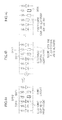
- Fig. 4 schematically shows repair with reverse bias application. Also in the repair with reverse bias application, I-mode repair and V-mode repair can be applied. Fig. 4 shows the case in which I-mode repair is performed before V-mode repair.
- the element representation parts with a hatch represent defected parts.
- the defect represented by diode element representation with a hatch represents a defect whose diode characteristics remain slightly, and the defect represented by a rectangle with a hatch represents a defect that does not exhibit diode characteristics.
- the charging layer 2 of the quantum cell 1 is constituted by a semiconductor of metal oxide, and does not become a semiconductor but an insulator unless electrons are coupled to the metal oxide.
- the material of the charging layer 2 includes a plurality of kinds of semiconductors, there exist VBG1, VBG2, ... (the value is smaller as the number of symbols is smaller) depending on the kinds, and there exist VBD1, VBD2, ..., as being unique to the respective semiconductors having values sufficiently larger than VBG.
- the current application direction is a direction in which a current flows in the order of the negative electrode 3, the charging layer 2, and the positive electrode 4, as shown in Fig. 4(B) .
- the controller 44 performs control to gradually increase a current value within a range in which the voltage between the electrodes 3 and 4 of the quantum cell 1 does not exceed VBGi (that is currently intended, among VBG1, VBG2, ...) while monitoring the voltage using the voltage meter 23. When the voltage exceeds VBGi, the controller 44 performs control to immediately return the current value to zero.
- the controller 44 controls such that, every time a current is increased, the current is kept during a certain period of time so that Joule heat is sufficiently transmitted to the short circuit section, and returns, even in such a period of time, the current value to zero once the measured voltage value varies and exceeds VBGi. If the controller 44 controls such that the voltage between the electrodes 3 and 4 becomes zero when the current is returned to zero (reset through a resistor, or connection of a zero voltage source, for example; Fig. 3 shows the configuration in the former case), it is possible to make residual electric charge of the quantum cell 1 generated by reverse bias application zero or make unnecessary charging empty, which prevents unexpected damages to the device (quantum cell) when the next step is performed.
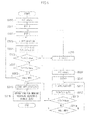
- Fig. 5 is a flowchart showing the processing of the controller 44 that executes the operation of reverse bias I-mode repair described above. The operation contents have been already explained, and thus the detailed explanation thereof with the use of Fig. 5 is omitted.
- the parameter notation in Fig. 5 is explained as follows.
- I represents an applied current
- Istart represents an initial applied current
- ⁇ I represents an increase amount of an applied current.
- TI1 represents a timer value for measuring the upper limit TI1max of time during which an applied current is made flow regardless of a value of the applied current I, and is updated in every unit time ⁇ TI.
- TI2 represents a timer value for measuring the upper limit TI2max of time during which an applied current of a currently-applied current value is made flow, and is updated in every unit time ⁇ TI.
- Vdet represents voltage detected by the voltage meter 23.
- the short circuit section DEF1 is detoxified by I-mode repair with reverse bias application, as shown in Fig. 4(B) .
- the reverse bias V-mode repair is performed after the reverse bias I-mode repair.
- the controller 44 applies a voltage due to the variable voltage source 31 on a portion between the electrodes 4 and 3 of the quantum cell 1 in the reverse bias direction (see Fig. 4(C) ), and gradually increases the value of an applied voltage while monitoring the current flowing at that time using the ammeter 33.
- a current flows unless a semiconductor sufficiently develops the characteristics.
- the controller 44 increases the value of an applied voltage until reaching VBGi, and returns, the applied voltage value to zero once when a current flows hardly. In this case, once the applied voltage value is returned to zero, no residual electric charge or unnecessary charging exists.
- the upper limit of operation time is set so that the operation time is not prolonged uselessly.
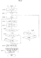
- Fig. 6 is a flowchart showing the processing of the controller 44 that executes the operation of reverse bias V-mode repair described above. The operation contents have been already explained, and thus the detailed explanation thereof with the use of Fig. 6 is omitted.
- the parameter notation in Fig. 6 is explained as follows.
- V represents an applied voltage
- Vstart represents an initial applied voltage
- ⁇ V represents an increase amount of an applied voltage.
- TV1 represents a timer value for measuring the upper limit TV1 max of time during which an applied voltage is applied regardless of a value of the applied voltage V, and is updated in every unit time ⁇ TV.
- TV2 represents a timer value for measuring the upper limit TV2max of time during which a current voltage value is applied, and is updated in every unit time ⁇ TV.
- Idet represents a current detected by the ammeter 33.
- the defects DEF2 and DEF3 with insufficient electronic coupling are detoxified by V-mode repair with reverse bias application in a way where the insufficiently-coupled electrons are cut off from atoms and the defected part almost becomes into an open state, as shown in Fig. 4(C) .
- Fig. 7 schematically shows repair with forward bias application. Also in the repair with forward bias application, I-mode repair and V-mode repair can be applied. Fig. 7 shows the case in which I-mode repair is performed before V-mode repair.
- the element representation parts with a hatch represent defected parts.
- the defect represented by quantum cell element representation with a hatch represents a defect whose quantum cell characteristics remain slightly
- the defect represented by diode element representation with a hatch represents a defect whose diode characteristics remain slightly
- the defect represented by a rectangle with a hatch represents a defect that does not exhibit diode characteristics.
- the difference from reverse bias application lies in that the quantum cell 1 performs an charging operation (and also performs a discharging operation depending on a case) by forward bias application (of any of a current and a voltage) as long as the quantum cell 1 is not in the complete short circuit state.
- the short circuit section is repaired by reverse bias current application.
- the short circuit section has pure resistance, it can be repaired by the same principle (by Joule heat) even when a forward bias current is made flow.
- the controller 44 gradually increases the value of an applied current of the variable current source 21 in a range of being equal to or less than a maximum allowable voltage for charging of the quantum cell 1, while monitoring the voltage between the electrodes 4 and 3 by output of the voltage meter 23.
- the application direction in this case is a forward bias direction as shown in Fig. 7(B) .
- the controller 44 gradually increases the value of an applied current of the variable current source 21 while monitoring the voltage between the electrodes 4 and 3, the current may flow in the section where electronic coupling is insufficient, which recovers coupling. Also in this case, the applied current value and the detection voltage value are controlled not to exceed the maximum allowable value for charging.
- the controller 44 lets a constant applied current flow from the variable current source 21 for a predetermined period of time, and returns, when the variation of a voltage value is within a set range, the applied current from the variable current source 21 to zero. At that time, the controller 44 controls such that the voltage between the electrodes 4 and 3 becomes zero (reset through a resistor or connection of a zero voltage source, for example; Fig.
- Fig. 8 is a flowchart showing the processing of the controller 44 that executes the operation of forward bias I-mode repair described above. The operation contents have been already explained, and thus the detailed explanation thereof with the use of Fig. 8 is omitted.
- the parameter notation in Fig. 8 is explained as follows.
- I represents an applied current
- Istart represents an initial applied current for detoxifying the short circuit section
- ⁇ I represents an increase amount of an applied current.
- Icost represents a constant applied current for recovering the coupling of a portion where electric coupling is insufficient.
- TI1 represents a timer value for measuring the upper limit TI1max of time during which an applied current is made flow for detoxifying the short circuit section regardless of a value of the applied current I, and is updated in every unit time ⁇ TI.
- TI2 represents a timer value for measuring the upper limit TI2max of time during which an applied current of a currently-applied current value is made flow for detoxifying the short circuit section, and is updated in every unit time ⁇ TI.
- TI3 represents a timer value for measuring a period of time during which a constant current value is made flow for recovering the coupling of a portion where electronic coupling is insufficient, and is updated in every unit time ⁇ TI.
- MAV represents a maximum allowable voltage for charging of the quantum cell 1.
- Vdet represents a voltage detected by the voltage meter 23.
- the short circuit section DEF11 is detoxified by I-mode repair with forward bias application, as shown in Fig. 7(B) .
- the quantum cell 1 includes defects DEF12 to DEF 14 where electronic coupling is insufficient as shown in Fig. 7(A)
- some of such defects may be recovered by I-mode repair with forward bias application in a way where electronic coupling becomes sufficient.
- the defect DEF14 is a defect in which electronic coupling is recovered by I-mode repair with forward bias application.
- the forward bias V-mode repair is performed after the forward bias I-mode repair.
- the controller 44 applies a voltage due to the variable voltage source 31 on a portion between the electrodes 4 and 3 of the quantum cell 1 in the forward bias direction (see Fig. 7(C) ), and gradually increases the value of an applied voltage while monitoring the current flowing at that time using the ammeter 33.
- the application of a voltage causes an electric field on the portion where electronic coupling is insufficient, which may recover the coupling.
- the portion hardly functions as a semiconductor, the insufficiently-coupled electrons may be cut off for detoxification.
- the applied voltage value and the detection current value are controlled not to exceed the maximum allowable value for charging.
- the controller 44 When the successive application of a plurality of constant voltages that requires predetermined total necessary time is finished without exceeding the setting range of the detection current value, the controller 44 returns the applied voltage value to zero. Also in this case, the controller 44 subsequently performs an operation to make the quantum cell 1 in the state with no residual electric charge and the state with empty charging by discharging through a resistor, etc. and then finishes the repair operation with forward bias voltage.
- Fig. 9 is a flowchart showing the processing of the controller 44 that executes the operation of forward bias V-mode repair described above. The operation contents have been already explained, and thus the detailed explanation thereof with the use of Fig. 9 is omitted.
- the parameter notation in Fig. 9 is explained as follows.
- V represents an applied voltage
- Vstart represents an initial applied voltage
- ⁇ V represents an increase amount of an applied voltage.
- TV1 represents a timer value for measuring the upper limit TV1max of time during which an applied voltage is applied regardless of a value of the applied voltage V, and is updated in every unit time ⁇ TV.
- TV2 represents a timer value for measuring the upper limit TV2max of time during which a current voltage value is applied, and is updated in every unit time ⁇ TV.
- Idet represents a current detected by the ammeter 33.
- MAV represents a maximum allowable voltage for charging of the quantum cell 1.
- MAI represents a maximum allowable current for charging of the quantum cell 1.
- the quantum cell 1 includes the defects DEF12 to DEF14 where electronic coupling is insufficient as shown in Fig. 7(A) , some of such defects are recovered in a way where electronic coupling becomes sufficient, while some of them are detoxified in a way where insufficiently-coupled electrons are cut off, by V-mode repair with forward bias application.
- the defect DEF13 represents a defect in which electronic coupling is recovered by V-mode repair with forward bias application.
- the defect DEF12 represents a defect detoxified in a way that insufficiently-coupled electrons are cut off by V-mode repair with forward bias application.
- the defects of the sheet type cell having semiconductor characteristics can be appropriately recovered and detoxified.
- the electrical repair applied in the above-described embodiment does not need such specification.
- the repair is performed by evaluating electrical characteristics after applying electrical stimulation that is preliminarily regarded as effective. Thus, it is not necessary to specify a position of the defect and physically repair the defect from the outside.
- the method of generating Joule heat in the short circuit section by reverse bias and evaporating or blackening (oxidizing) foreign substances to make the short circuit section open is applied, and in addition, the operation for cutting off insufficient electronic coupling or making coupling sufficient is performed. Therefore, it is possible to not only merely detoxify the defect but also improve the efficiency of the sheet type cell.
- the controller controls such that, when the kinds of electrical stimulation are switched, new kind of electrical stimulation is applied between the positive electrode and the negative electrode after the empty state is realized or residual electric charge is released (see S110 in Fig. 5 , S211 in Fig. 6 , and S316 in Fig. 8 ).
- the operation by the empty state realization means in claims includes at least one of realization of empty electric charge and release of residual electric charge. Therefore, it is possible to prevent unexpected damages to the device even when the electrical stimulation is switched to a new kind.
- the controller controls such that all kinds of electrical stimulation to which the electrical stimulation source of the repair apparatus is adaptive are sequentially applied between the positive electrode and the negative electrode of the quantum cell (reverse bias I-mode repair, reverse bias V-mode repair, forward bias I-mode repair, and forward bias V-mode repair).
- reverse bias I-mode repair reverse bias V-mode repair
- forward bias I-mode repair forward bias V-mode repair
- forward bias V-mode repair forward bias V-mode repair
- the present invention is not limited to the above-described embodiment. Hereinafter, some variant embodiments will be exemplified.
- Fig. 10 is a block diagram showing a repair apparatus 10A of a variant example that is adaptive to P-mode repair, in which the same numerals and symbols will be used to designate the same or corresponding components as those in Fig. 3 showing the repair apparatus 10 of the above-described embodiment.
- a controller 44A controls such that a constant current value is made flow by the variable current source 21 (direction is also defined) and a constant voltage value is applied by the variable voltage source 31 (direction is also defined), whereby constant power can be applied (made flow) to the quantum cell 1 to be repaired. That is, P-mode repair can be performed.
- controller 44A controls such that the variable voltage source 31 does not apply a constant voltage and the variable current source 21 supplies a constant value of current, whereby I-mode repair can be performed.
- controller 44A controls such that the variable current source 21 does not supply a constant current and the variable voltage source 31 applies a constant value of voltage, whereby V-mode repair can be performed.
- variable current source or the variable voltage source which is an electrical stimulation source
- the variable current source or the variable voltage source outputs a DC current or DC voltage specified at that time.
- an arbitrary waveform generator AMG
- AC stimulation is applied as well as DC stimulation. Examples thereof include sine waves, square waves, sawtooth waves, and pulse waves. It is considered that energy due to frequency components is added to a DC current and a DC voltage, which makes it possible to efficiently perform the repair operation.
Landscapes
- Chemical & Material Sciences (AREA)
- Chemical Kinetics & Catalysis (AREA)
- Electrochemistry (AREA)
- General Chemical & Material Sciences (AREA)
- Engineering & Computer Science (AREA)
- Manufacturing & Machinery (AREA)
- Microelectronics & Electronic Packaging (AREA)
- Secondary Cells (AREA)
- Testing Or Measuring Of Semiconductors Or The Like (AREA)
- Charge And Discharge Circuits For Batteries Or The Like (AREA)
- Photovoltaic Devices (AREA)
Applications Claiming Priority (1)
| Application Number | Priority Date | Filing Date | Title |
|---|---|---|---|
| PCT/JP2011/076200 WO2013072988A1 (ja) | 2011-11-14 | 2011-11-14 | シート状電池のリペア装置 |
Publications (3)
| Publication Number | Publication Date |
|---|---|
| EP2782183A1 true EP2782183A1 (de) | 2014-09-24 |
| EP2782183A4 EP2782183A4 (de) | 2015-09-23 |
| EP2782183B1 EP2782183B1 (de) | 2019-11-13 |
Family
ID=48429102
Family Applications (1)
| Application Number | Title | Priority Date | Filing Date |
|---|---|---|---|
| EP11875625.3A Not-in-force EP2782183B1 (de) | 2011-11-14 | 2011-11-14 | Reparaturvorrichtung für blattförmige batterie |
Country Status (8)
| Country | Link |
|---|---|
| US (1) | US9799927B2 (de) |
| EP (1) | EP2782183B1 (de) |
| JP (1) | JP5990533B2 (de) |
| KR (1) | KR101484055B1 (de) |
| CN (1) | CN103959548B (de) |
| CA (1) | CA2854909C (de) |
| TW (1) | TWI514601B (de) |
| WO (1) | WO2013072988A1 (de) |
Family Cites Families (19)
| Publication number | Priority date | Publication date | Assignee | Title |
|---|---|---|---|---|
| US4464823A (en) * | 1982-10-21 | 1984-08-14 | Energy Conversion Devices, Inc. | Method for eliminating short and latent short circuit current paths in photovoltaic devices |
| AU2042183A (en) | 1983-08-03 | 1985-02-07 | Energy Conversion Devices Inc. | Eliminating short circuits in photovoltaic devices |
| AU580903B2 (en) | 1986-01-29 | 1989-02-02 | Semiconductor Energy Laboratory Co. Ltd. | Method for manufacturing photoelectric conversion devices |
| JPS6388869A (ja) | 1986-10-01 | 1988-04-19 | Kanegafuchi Chem Ind Co Ltd | アモルファス太陽電池のピンホール消滅装置 |
| JPH053333A (ja) * | 1991-06-25 | 1993-01-08 | Canon Inc | 太陽電池のリペア方法 |
| JP3740618B2 (ja) * | 1996-06-17 | 2006-02-01 | 株式会社カネカ | 太陽電池の短絡部除去方法及び該短絡部除去装置 |
| JPH11204816A (ja) * | 1998-01-20 | 1999-07-30 | Kanegafuchi Chem Ind Co Ltd | 半導体薄膜光電変換装置の製造方法 |
| JP3050546B1 (ja) | 1999-03-24 | 2000-06-12 | 鐘淵化学工業株式会社 | 太陽電池の短絡部除去方法 |
| JP4627575B2 (ja) | 1999-08-12 | 2011-02-09 | 株式会社カネカ | 太陽電池の短絡部除去方法 |
| JP3143616B2 (ja) * | 1999-08-12 | 2001-03-07 | 鐘淵化学工業株式会社 | 太陽電池の短絡部除去方法 |
| AU766466B2 (en) | 1999-05-14 | 2003-10-16 | Kaneka Corporation | Reverse biasing apparatus for solar battery module |
| JP2003215190A (ja) * | 2001-11-16 | 2003-07-30 | Hioki Ee Corp | ショート検出装置 |
| JP4221479B2 (ja) | 2002-05-09 | 2009-02-12 | 富士電機システムズ株式会社 | 薄膜太陽電池モジュールの製造方法 |
| JP4887664B2 (ja) | 2005-05-17 | 2012-02-29 | ソニー株式会社 | 多孔質構造体の製造方法及び光電変換素子の製造方法 |
| JP2006332469A (ja) * | 2005-05-27 | 2006-12-07 | Peccell Technologies Inc | 光充電可能な積層型キャパシタ |
| JP5297809B2 (ja) | 2006-11-02 | 2013-09-25 | グエラテクノロジー株式会社 | 電界感応素子およびそれを用いた表示デバイス |
| JP5288368B2 (ja) * | 2007-11-30 | 2013-09-11 | 独立行政法人物質・材料研究機構 | 太陽電池 |
| JP5476641B2 (ja) * | 2009-09-03 | 2014-04-23 | 株式会社日本マイクロニクス | 電池短絡部除去装置及び方法、並びに、電池短絡部除去電圧決定装置及び方法 |
| US20120288968A1 (en) * | 2011-05-12 | 2012-11-15 | Ming-Teng Hsieh | Method for repairing a semiconductor structure having a current-leakage issue |
-
2011
- 2011-11-14 WO PCT/JP2011/076200 patent/WO2013072988A1/ja not_active Ceased
- 2011-11-14 EP EP11875625.3A patent/EP2782183B1/de not_active Not-in-force
- 2011-11-14 CN CN201180074825.2A patent/CN103959548B/zh not_active Expired - Fee Related
- 2011-11-14 JP JP2013544005A patent/JP5990533B2/ja not_active Expired - Fee Related
- 2011-11-14 KR KR1020147011124A patent/KR101484055B1/ko not_active Expired - Fee Related
- 2011-11-14 US US14/357,856 patent/US9799927B2/en not_active Expired - Fee Related
- 2011-11-14 CA CA2854909A patent/CA2854909C/en not_active Expired - Fee Related
-
2012
- 2012-04-23 TW TW101114375A patent/TWI514601B/zh not_active IP Right Cessation
Also Published As
| Publication number | Publication date |
|---|---|
| JP5990533B2 (ja) | 2016-09-14 |
| EP2782183A4 (de) | 2015-09-23 |
| KR101484055B1 (ko) | 2015-01-20 |
| CA2854909A1 (en) | 2013-05-23 |
| US20150000119A1 (en) | 2015-01-01 |
| WO2013072988A1 (ja) | 2013-05-23 |
| CN103959548A (zh) | 2014-07-30 |
| CA2854909C (en) | 2018-01-30 |
| TWI514601B (zh) | 2015-12-21 |
| KR20140082739A (ko) | 2014-07-02 |
| TW201320368A (zh) | 2013-05-16 |
| CN103959548B (zh) | 2017-02-15 |
| JPWO2013072988A1 (ja) | 2015-04-02 |
| EP2782183B1 (de) | 2019-11-13 |
| US9799927B2 (en) | 2017-10-24 |
Similar Documents
| Publication | Publication Date | Title |
|---|---|---|
| KR101635097B1 (ko) | 충방전 장치 | |
| CN115989614A (zh) | 用于使可充电电池放电的可充电电池放电装置和用于使多个可充电电池放电的方法 | |
| KR102784889B1 (ko) | 단로기를 이용한 전류 차단 장치 및 방법 | |
| CN104052095A (zh) | 蓄电池单池单元以及用于监控蓄电池单池的方法 | |
| KR20200004651A (ko) | 이차전지 내부단락 시험 방법과 장치 및 이에 이용되는 내부단락 시험용 이차전지 | |
| Meng et al. | On-line model-based short circuit diagnosis of lithium-ion batteries for electric vehicle application | |
| Fatullah et al. | Analysis of discharge rate and ambient temperature effects on lead acid battery capacity | |
| JP5840218B2 (ja) | 太陽光発電機の電位を設定するための回路装置 | |
| EP2782183B1 (de) | Reparaturvorrichtung für blattförmige batterie | |
| CN113315198A (zh) | 一种可替换铅酸蓄电池使用的锂电池装置 | |
| JP6240634B2 (ja) | バイパスダイオードの故障検査装置 | |
| KR102538244B1 (ko) | 다이오드를 이용한 배터리 이상 방지 장치 및 방법 | |
| CN102569920B (zh) | 一种蓄电池组远程在线修复监控装置 | |
| US12255471B2 (en) | Method for operating a contactor | |
| CN110816312B (zh) | 用于运行电池组系统的方法和电动车辆 | |
| CN223992956U (zh) | 一种检测电路和功率变换器 | |
| CN110609240A (zh) | 检测设备和用于运行检测设备的方法 | |
| Truong et al. | Resonance Frequency-Based Desulfator Design for Lead-Acid Batteries | |
| US10298041B2 (en) | Electronic connect/disconnect device and method for a high voltage battery | |
| RU62292U1 (ru) | Первичная литиевая батарея (варианты) | |
| KR20250039534A (ko) | 폐배터리 완전 방전 방법 | |
| Puzakov | Results of Simulation of Faults of Starter Batteries | |
| RU39745U1 (ru) | Первичная литиевая батарея (варианты) | |
| WO2026052824A1 (fr) | Procédé de test d'un disjoncteur haute tension muni d'un circuit d'injection | |
| Mojsoska | Stationary ACCU batteries for uninterrupted power supply system of the power facilities |
Legal Events
| Date | Code | Title | Description |
|---|---|---|---|
| PUAI | Public reference made under article 153(3) epc to a published international application that has entered the european phase |
Free format text: ORIGINAL CODE: 0009012 |
|
| 17P | Request for examination filed |
Effective date: 20140521 |
|
| AK | Designated contracting states |
Kind code of ref document: A1 Designated state(s): AL AT BE BG CH CY CZ DE DK EE ES FI FR GB GR HR HU IE IS IT LI LT LU LV MC MK MT NL NO PL PT RO RS SE SI SK SM TR |
|
| DAX | Request for extension of the european patent (deleted) | ||
| RA4 | Supplementary search report drawn up and despatched (corrected) |
Effective date: 20150821 |
|
| RIC1 | Information provided on ipc code assigned before grant |
Ipc: H01L 31/18 20060101ALI20150814BHEP Ipc: H01M 10/42 20060101AFI20150814BHEP Ipc: H01L 31/20 20060101ALI20150814BHEP |
|
| STAA | Information on the status of an ep patent application or granted ep patent |
Free format text: STATUS: EXAMINATION IS IN PROGRESS |
|
| 17Q | First examination report despatched |
Effective date: 20181106 |
|
| GRAP | Despatch of communication of intention to grant a patent |
Free format text: ORIGINAL CODE: EPIDOSNIGR1 |
|
| STAA | Information on the status of an ep patent application or granted ep patent |
Free format text: STATUS: GRANT OF PATENT IS INTENDED |
|
| INTG | Intention to grant announced |
Effective date: 20190731 |
|
| RIN1 | Information on inventor provided before grant (corrected) |
Inventor name: TERAKADO, NOBUAKI Inventor name: NAKAZAWA, AKIRA Inventor name: HIWADA, KIYOYASU Inventor name: DEWA, HARUTADA |
|
| GRAS | Grant fee paid |
Free format text: ORIGINAL CODE: EPIDOSNIGR3 |
|
| GRAA | (expected) grant |
Free format text: ORIGINAL CODE: 0009210 |
|
| STAA | Information on the status of an ep patent application or granted ep patent |
Free format text: STATUS: THE PATENT HAS BEEN GRANTED |
|
| AK | Designated contracting states |
Kind code of ref document: B1 Designated state(s): AL AT BE BG CH CY CZ DE DK EE ES FI FR GB GR HR HU IE IS IT LI LT LU LV MC MK MT NL NO PL PT RO RS SE SI SK SM TR |
|
| REG | Reference to a national code |
Ref country code: CH Ref legal event code: EP Ref country code: AT Ref legal event code: REF Ref document number: 1202631 Country of ref document: AT Kind code of ref document: T Effective date: 20191115 |
|
| REG | Reference to a national code |
Ref country code: DE Ref legal event code: R096 Ref document number: 602011063429 Country of ref document: DE |
|
| REG | Reference to a national code |
Ref country code: IE Ref legal event code: FG4D |
|
| REG | Reference to a national code |
Ref country code: NL Ref legal event code: MP Effective date: 20191113 |
|
| REG | Reference to a national code |
Ref country code: LT Ref legal event code: MG4D |
|
| PG25 | Lapsed in a contracting state [announced via postgrant information from national office to epo] |
Ref country code: LV Free format text: LAPSE BECAUSE OF FAILURE TO SUBMIT A TRANSLATION OF THE DESCRIPTION OR TO PAY THE FEE WITHIN THE PRESCRIBED TIME-LIMIT Effective date: 20191113 Ref country code: SE Free format text: LAPSE BECAUSE OF FAILURE TO SUBMIT A TRANSLATION OF THE DESCRIPTION OR TO PAY THE FEE WITHIN THE PRESCRIBED TIME-LIMIT Effective date: 20191113 Ref country code: ES Free format text: LAPSE BECAUSE OF FAILURE TO SUBMIT A TRANSLATION OF THE DESCRIPTION OR TO PAY THE FEE WITHIN THE PRESCRIBED TIME-LIMIT Effective date: 20191113 Ref country code: NL Free format text: LAPSE BECAUSE OF FAILURE TO SUBMIT A TRANSLATION OF THE DESCRIPTION OR TO PAY THE FEE WITHIN THE PRESCRIBED TIME-LIMIT Effective date: 20191113 Ref country code: GR Free format text: LAPSE BECAUSE OF FAILURE TO SUBMIT A TRANSLATION OF THE DESCRIPTION OR TO PAY THE FEE WITHIN THE PRESCRIBED TIME-LIMIT Effective date: 20200214 Ref country code: PT Free format text: LAPSE BECAUSE OF FAILURE TO SUBMIT A TRANSLATION OF THE DESCRIPTION OR TO PAY THE FEE WITHIN THE PRESCRIBED TIME-LIMIT Effective date: 20200313 Ref country code: LT Free format text: LAPSE BECAUSE OF FAILURE TO SUBMIT A TRANSLATION OF THE DESCRIPTION OR TO PAY THE FEE WITHIN THE PRESCRIBED TIME-LIMIT Effective date: 20191113 Ref country code: NO Free format text: LAPSE BECAUSE OF FAILURE TO SUBMIT A TRANSLATION OF THE DESCRIPTION OR TO PAY THE FEE WITHIN THE PRESCRIBED TIME-LIMIT Effective date: 20200213 Ref country code: PL Free format text: LAPSE BECAUSE OF FAILURE TO SUBMIT A TRANSLATION OF THE DESCRIPTION OR TO PAY THE FEE WITHIN THE PRESCRIBED TIME-LIMIT Effective date: 20191113 Ref country code: BG Free format text: LAPSE BECAUSE OF FAILURE TO SUBMIT A TRANSLATION OF THE DESCRIPTION OR TO PAY THE FEE WITHIN THE PRESCRIBED TIME-LIMIT Effective date: 20200213 Ref country code: FI Free format text: LAPSE BECAUSE OF FAILURE TO SUBMIT A TRANSLATION OF THE DESCRIPTION OR TO PAY THE FEE WITHIN THE PRESCRIBED TIME-LIMIT Effective date: 20191113 |
|
| PGFP | Annual fee paid to national office [announced via postgrant information from national office to epo] |
Ref country code: DE Payment date: 20200110 Year of fee payment: 9 |
|
| PG25 | Lapsed in a contracting state [announced via postgrant information from national office to epo] |
Ref country code: RS Free format text: LAPSE BECAUSE OF FAILURE TO SUBMIT A TRANSLATION OF THE DESCRIPTION OR TO PAY THE FEE WITHIN THE PRESCRIBED TIME-LIMIT Effective date: 20191113 Ref country code: HR Free format text: LAPSE BECAUSE OF FAILURE TO SUBMIT A TRANSLATION OF THE DESCRIPTION OR TO PAY THE FEE WITHIN THE PRESCRIBED TIME-LIMIT Effective date: 20191113 Ref country code: IS Free format text: LAPSE BECAUSE OF FAILURE TO SUBMIT A TRANSLATION OF THE DESCRIPTION OR TO PAY THE FEE WITHIN THE PRESCRIBED TIME-LIMIT Effective date: 20200313 |
|
| PG25 | Lapsed in a contracting state [announced via postgrant information from national office to epo] |
Ref country code: AL Free format text: LAPSE BECAUSE OF FAILURE TO SUBMIT A TRANSLATION OF THE DESCRIPTION OR TO PAY THE FEE WITHIN THE PRESCRIBED TIME-LIMIT Effective date: 20191113 |
|
| PGFP | Annual fee paid to national office [announced via postgrant information from national office to epo] |
Ref country code: FR Payment date: 20200113 Year of fee payment: 9 |
|
| REG | Reference to a national code |
Ref country code: CH Ref legal event code: PL |
|
| PG25 | Lapsed in a contracting state [announced via postgrant information from national office to epo] |
Ref country code: LI Free format text: LAPSE BECAUSE OF NON-PAYMENT OF DUE FEES Effective date: 20191130 Ref country code: RO Free format text: LAPSE BECAUSE OF FAILURE TO SUBMIT A TRANSLATION OF THE DESCRIPTION OR TO PAY THE FEE WITHIN THE PRESCRIBED TIME-LIMIT Effective date: 20191113 Ref country code: CZ Free format text: LAPSE BECAUSE OF FAILURE TO SUBMIT A TRANSLATION OF THE DESCRIPTION OR TO PAY THE FEE WITHIN THE PRESCRIBED TIME-LIMIT Effective date: 20191113 Ref country code: CH Free format text: LAPSE BECAUSE OF NON-PAYMENT OF DUE FEES Effective date: 20191130 Ref country code: EE Free format text: LAPSE BECAUSE OF FAILURE TO SUBMIT A TRANSLATION OF THE DESCRIPTION OR TO PAY THE FEE WITHIN THE PRESCRIBED TIME-LIMIT Effective date: 20191113 Ref country code: DK Free format text: LAPSE BECAUSE OF FAILURE TO SUBMIT A TRANSLATION OF THE DESCRIPTION OR TO PAY THE FEE WITHIN THE PRESCRIBED TIME-LIMIT Effective date: 20191113 Ref country code: LU Free format text: LAPSE BECAUSE OF NON-PAYMENT OF DUE FEES Effective date: 20191114 |
|
| REG | Reference to a national code |
Ref country code: DE Ref legal event code: R097 Ref document number: 602011063429 Country of ref document: DE |
|
| REG | Reference to a national code |
Ref country code: AT Ref legal event code: MK05 Ref document number: 1202631 Country of ref document: AT Kind code of ref document: T Effective date: 20191113 |
|
| REG | Reference to a national code |
Ref country code: BE Ref legal event code: MM Effective date: 20191130 |
|
| PG25 | Lapsed in a contracting state [announced via postgrant information from national office to epo] |
Ref country code: SK Free format text: LAPSE BECAUSE OF FAILURE TO SUBMIT A TRANSLATION OF THE DESCRIPTION OR TO PAY THE FEE WITHIN THE PRESCRIBED TIME-LIMIT Effective date: 20191113 Ref country code: SM Free format text: LAPSE BECAUSE OF FAILURE TO SUBMIT A TRANSLATION OF THE DESCRIPTION OR TO PAY THE FEE WITHIN THE PRESCRIBED TIME-LIMIT Effective date: 20191113 Ref country code: MC Free format text: LAPSE BECAUSE OF FAILURE TO SUBMIT A TRANSLATION OF THE DESCRIPTION OR TO PAY THE FEE WITHIN THE PRESCRIBED TIME-LIMIT Effective date: 20191113 |
|
| PLBE | No opposition filed within time limit |
Free format text: ORIGINAL CODE: 0009261 |
|
| STAA | Information on the status of an ep patent application or granted ep patent |
Free format text: STATUS: NO OPPOSITION FILED WITHIN TIME LIMIT |
|
| 26N | No opposition filed |
Effective date: 20200814 |
|
| GBPC | Gb: european patent ceased through non-payment of renewal fee |
Effective date: 20200213 |
|
| PG25 | Lapsed in a contracting state [announced via postgrant information from national office to epo] |
Ref country code: IE Free format text: LAPSE BECAUSE OF NON-PAYMENT OF DUE FEES Effective date: 20191114 |
|
| PG25 | Lapsed in a contracting state [announced via postgrant information from national office to epo] |
Ref country code: BE Free format text: LAPSE BECAUSE OF NON-PAYMENT OF DUE FEES Effective date: 20191130 Ref country code: AT Free format text: LAPSE BECAUSE OF FAILURE TO SUBMIT A TRANSLATION OF THE DESCRIPTION OR TO PAY THE FEE WITHIN THE PRESCRIBED TIME-LIMIT Effective date: 20191113 Ref country code: SI Free format text: LAPSE BECAUSE OF FAILURE TO SUBMIT A TRANSLATION OF THE DESCRIPTION OR TO PAY THE FEE WITHIN THE PRESCRIBED TIME-LIMIT Effective date: 20191113 |
|
| PG25 | Lapsed in a contracting state [announced via postgrant information from national office to epo] |
Ref country code: IT Free format text: LAPSE BECAUSE OF FAILURE TO SUBMIT A TRANSLATION OF THE DESCRIPTION OR TO PAY THE FEE WITHIN THE PRESCRIBED TIME-LIMIT Effective date: 20191113 Ref country code: GB Free format text: LAPSE BECAUSE OF NON-PAYMENT OF DUE FEES Effective date: 20200213 |
|
| PG25 | Lapsed in a contracting state [announced via postgrant information from national office to epo] |
Ref country code: CY Free format text: LAPSE BECAUSE OF FAILURE TO SUBMIT A TRANSLATION OF THE DESCRIPTION OR TO PAY THE FEE WITHIN THE PRESCRIBED TIME-LIMIT Effective date: 20191113 |
|
| REG | Reference to a national code |
Ref country code: DE Ref legal event code: R119 Ref document number: 602011063429 Country of ref document: DE |
|
| PG25 | Lapsed in a contracting state [announced via postgrant information from national office to epo] |
Ref country code: HU Free format text: LAPSE BECAUSE OF FAILURE TO SUBMIT A TRANSLATION OF THE DESCRIPTION OR TO PAY THE FEE WITHIN THE PRESCRIBED TIME-LIMIT; INVALID AB INITIO Effective date: 20111114 Ref country code: MT Free format text: LAPSE BECAUSE OF FAILURE TO SUBMIT A TRANSLATION OF THE DESCRIPTION OR TO PAY THE FEE WITHIN THE PRESCRIBED TIME-LIMIT Effective date: 20191113 |
|
| PG25 | Lapsed in a contracting state [announced via postgrant information from national office to epo] |
Ref country code: FR Free format text: LAPSE BECAUSE OF NON-PAYMENT OF DUE FEES Effective date: 20201130 |
|
| PG25 | Lapsed in a contracting state [announced via postgrant information from national office to epo] |
Ref country code: DE Free format text: LAPSE BECAUSE OF NON-PAYMENT OF DUE FEES Effective date: 20210601 |
|
| PG25 | Lapsed in a contracting state [announced via postgrant information from national office to epo] |
Ref country code: TR Free format text: LAPSE BECAUSE OF FAILURE TO SUBMIT A TRANSLATION OF THE DESCRIPTION OR TO PAY THE FEE WITHIN THE PRESCRIBED TIME-LIMIT Effective date: 20191113 |
|
| PG25 | Lapsed in a contracting state [announced via postgrant information from national office to epo] |
Ref country code: MK Free format text: LAPSE BECAUSE OF FAILURE TO SUBMIT A TRANSLATION OF THE DESCRIPTION OR TO PAY THE FEE WITHIN THE PRESCRIBED TIME-LIMIT Effective date: 20191113 |