EP2784875A1 - Antenne et appareil de communication sans fil - Google Patents
Antenne et appareil de communication sans fil Download PDFInfo
- Publication number
- EP2784875A1 EP2784875A1 EP14160912.3A EP14160912A EP2784875A1 EP 2784875 A1 EP2784875 A1 EP 2784875A1 EP 14160912 A EP14160912 A EP 14160912A EP 2784875 A1 EP2784875 A1 EP 2784875A1
- Authority
- EP
- European Patent Office
- Prior art keywords
- layer
- antenna
- inductor
- wireless communication
- communication apparatus
- Prior art date
- Legal status (The legal status is an assumption and is not a legal conclusion. Google has not performed a legal analysis and makes no representation as to the accuracy of the status listed.)
- Granted
Links
Images


Classifications
-
- H—ELECTRICITY
- H01—ELECTRIC ELEMENTS
- H01Q—ANTENNAS, i.e. RADIO AERIALS
- H01Q15/00—Devices for reflection, refraction, diffraction or polarisation of waves radiated from an antenna, e.g. quasi-optical devices
- H01Q15/0006—Devices acting selectively as reflecting surface, as diffracting or as refracting device, e.g. frequency filtering or angular spatial filtering devices
- H01Q15/0086—Devices acting selectively as reflecting surface, as diffracting or as refracting device, e.g. frequency filtering or angular spatial filtering devices said selective devices having materials with a synthesized negative refractive index, e.g. metamaterials or left-handed materials
-
- H—ELECTRICITY
- H01—ELECTRIC ELEMENTS
- H01Q—ANTENNAS, i.e. RADIO AERIALS
- H01Q1/00—Details of, or arrangements associated with, antennas
- H01Q1/36—Structural form of radiating elements, e.g. cone, spiral, umbrella; Particular materials used therewith
Definitions
- the embodiment discussed herein is related to an antenna and a wireless communication apparatus.
- an antenna is disposed away from the ground so that influence of the ground on the antenna is reduced. Furthermore, a technique has been widely used in which a magnetic wall for absorbing electromagnetic waves is disposed between the ground and an antenna (refer to Japanese Laid-open Patent Publication No. 2011-55054 , for example). Furthermore, a technique has been widely used in which reduction of electromagnetic interference between antennas and between devices implemented on a printed circuit board is achieved by forming an electromagnetic bandgap structure which suppresses propagation of electromagnetic waves in a specific frequency band (refer to International Publication Pamphlet No. WO 2010/013496 , for example).
- a metamaterial has been widely known which is composed by arranging material pieces at intervals smaller than a wavelength of electromagnetic waves to obtain an electric characteristic and a magnetic characteristic different from those of the original material pieces.
- a technique has been known which forms a magnetic wall by a metamaterial in which a plurality of mushroom-shaped structures, in which a ground and conductors are connected to each other by vias, are periodically arranged (refer to SANADA Atsushi, tutorial "What is Metamaterials", November 17 issue of Nikkei Electronics, pp. 128 to 134, Japan, 2008 , SANADA Atsushi, tutorial “What is Metamaterials", December 15 issue of Nikkei Electronics, pp.
- an antenna includes a first layer including a pattern so as to configure an inductor, a second layer forming capacitance that is electrically coupled with inductance of the inductor; and a third layer configuring an electric wall, the first layer being disposed between the third layer and the first layer.
- FIG. 1 is a diagram illustrating a first example of an antenna according to an embodiment.
- FIG. 2 is a diagram illustrating each layer in the antenna in FIG. 1 .
- FIG. 3 is a sectional view schematically illustrating the antenna of FIG. 1 .
- dielectric layers interposed between conductive layers are omitted.
- an antenna 1 includes a first layer 2 including a pattern serving as an inductor, a second layer 3 which is used to hold capacitance between the second layer 3 and inductance of the inductor, and a third layer 4 constituting an electric wall.
- the antenna 1 further includes an antenna conductive layer 5 formed by a conductor on an uppermost surface, for example.
- a first dielectric layer 6 formed by a dielectric body is disposed beneath the antenna conductive layer 5 so as to be contact with the antenna conductive layer 5.
- the second layer 3 formed by a conductive body is disposed beneath the first dielectric layer 6 so as to be contact with the first dielectric layer 6.
- a second dielectric layer 7 formed by a dielectric body is disposed beneath the second layer 3 so as to be contact with the second layer 3.
- the first layer 2 formed by a conductive body is disposed beneath the second dielectric layer 7 so as to be contact with the second dielectric layer 7.
- a third dielectric layer 8 formed by a dielectric body is disposed beneath the first layer 2 so as to be contact with the first layer 2.
- the third layer 4 formed by a conductive body is disposed beneath the third dielectric layer 8 so as to be contact with the third dielectric layer 8.
- the antenna 1 is configured by laminating the third layer 4, the third dielectric layer 8, the first layer 2, the second dielectric layer 7, the second layer 3, the first dielectric layer 6, and the antenna conductive layer 5 in this order from the bottom.
- the first dielectric layer 6, the second dielectric layer 7, and the third dielectric layer 8 may be air layers.
- the inductor includes a structure such that a plurality of unit elements smaller than a wavelength of electromagnetic wave are arranged, and is formed by a left-handed metamaterial which has negative permittivity and negative permeability, where the electromagnetic wave is preferably corresponding to one used for a wireless radio frequency for example.
- the number of unit elements is determined in accordance with a frequency of the electromagnetic waves.
- Each of the unit elements included in the inductor may have a wiring pattern of a spiral shape, for example.
- each of the unit elements included in the inductor may have a wiring pattern of a meander shape, for example, as illustrated in FIG. 4 which is a diagram illustrating the alternative pattern of the inductor of the antenna according to the embodiment.
- capacitance is generated between the third layer 4 and the first layer 2, between the first layer 2 and the second layer 3, and between the second layer 3 and the antenna conductive layer 5.
- the third layer 4 and one end of the first layer 2 may be set to the ground potential.
- the first layer 2 and the second layer 3 form a magnetic wall by inductance generated by the first layer 2 and the capacitance generated between the first layer 2 and the second layer 3.
- FIG. 5 is a diagram illustrating an equivalent circuit of the antenna 1 of FIG. 1 .
- the electric wall is formed by a conductive layer functioning as a ground potential GND, for example, beneath an antenna conductive layer.
- the magnetic wall is formed by an inductor 11 and a capacitance12 which are coupled to each other in parallel, where one end of the inductor 11 and one end of the capacitance 12 are set to the ground potential, for example.
- the magnetic wall has a characteristic in which permittivity and permeability are both negative values.
- FIG. 6 is a diagram illustrating layers of an antenna in a second example according to the embodiment, in which each of the layers are depicted separately.
- FIG. 7 is a sectional view schematically illustrating the antenna of FIG. 6 .
- dielectric layers interposed between conductive layers are omitted.
- the antenna 1 includes a first layer 2 including a pattern for an inductor, a second layer 3 which is used to hold capacitance between the second layer 3 and inductance of the inductor, and a third layer 4 constituting an electric wall.
- the antenna 1 further includes a fourth layer 21 including a pattern for an inductor and a fifth layer 22 which is used to hold capacitance between the fifth layer 22 and inductance of the inductor of the fourth layer 21.
- the antenna 1 further includes an antenna conductive layer 5 formed by a conductor on an uppermost surface thereof, for example.
- a first dielectric layer formed by a dielectric body, not illustrated, is disposed beneath the antenna conductive layer 5 so as to be contact with the antenna conductive layer 5.
- the fifth layer 22 is formed of a conductive body and disposed beneath the first dielectric layer, not illustrated, so as to be contact with the first dielectric layer.
- a fourth dielectric layer formed by a dielectric body, not illustrated, is disposed beneath the fifth layer 22 so as to be contact with the fifth layer 22.
- the fourth layer 21 is formed of a conductive body and disposed beneath the fourth dielectric layer, not illustrated, so as to be contact with the fourth dielectric layer.
- a fifth dielectric layer is formed of a dielectric body, not illustrated, and disposed beneath the fourth layer 21 so as to be contact with the fourth layer 21.
- the second layer 3 is formed of a conductive body and disposed beneath the fifth dielectric layer, not illustrated, so as to be contact with the fifth dielectric layer.
- a second dielectric layer is formed of a dielectric body, not illustrated, and disposed beneath the second layer 3 so as to be contact with the second layer 3.
- the first layer 2 is formed of a conductive body and disposed beneath the second dielectric layer, not illustrated, so as to be contact with the second dielectric layer.
- a third dielectric layer is formed of a dielectric body, not illustrated, and disposed beneath the first layer 2 so as to be contact with the first layer 2.
- the third layer 4 is formed of a conductive body and disposed beneath the third dielectric layer, not illustrated, so as to be contact with the third dielectric layer.
- the antenna 1 is configured by laminating the third layer 4, the third dielectric layer, the first layer 2, the second dielectric layer, the second layer 3, the fifth dielectric layer, the fourth layer 21, the fourth dielectric layer, the fifth layer 22, the first dielectric layer, and the antenna conductive layer 5 in this order from the bottom.
- the dielectric layers may be air layers.
- the inductor is formed by a left-handed metamaterial which is configured such that a plurality of unit elements smaller than a wavelength of electromagnetic wave are arranged and which has negative permittivity and negative permeability, where the electromagnetic wave is preferably corresponding to one used for a wireless radio frequency.
- the unit elements included in the inductor may include a wiring pattern of a spiral shape, for example.
- the unit elements of the inductor may include a wiring pattern of a meander shape, for example, as illustrated in FIG. 4 .
- each capacitance is generated respectively between the third layer 4 and the first layer 2, between the first layer 2 and the second layer 3, between the second layer 3 and the fourth layer 21, between the fourth layer 21 and the fifth layer 22, and between the fifth layer 22 and the antenna conductive layer 5.
- the third layer 4, one end of the first layer 2, and one end of the fourth layer 21 may include the ground potential.
- the first layer 2 and the second layer 3 form a magnetic wall by inductance generated by the first layer 2 and the capacitance generated between the first layer 2 and the second layer 3.
- the fourth layer 21 and the fifth layer 22 form a magnetic wall by inductance generated by the fourth layer 21 and the capacitance generated between the fourth layer 21 and the fifth layer 22.
- FIG. 8 is a diagram illustrating an equivalent circuit of the antenna 1 of FIG. 6 .
- the electric wall is formed by a conductive layer having a ground potential GND, for example, under an antenna conductive layer.
- the magnetic walls are formed by an inductor 11 and a capacitance 12 which are connected to each other in parallel and an inductor 13 and a capacitance 14 which are connected to each other in parallel.
- One end of the inductor 11, one end of the capacitance 12, one end of the inductor 13, and one end of the capacitance 14 have the ground potential, for example.
- the magnetic walls have a characteristic in which permittivity and permeability are both negative values. It is preferable for the antenna 1 to include further a similar magnetic wall which includes a layer including a pattern for an inductor and an additional layer which is used to hold capacitance between the additional layer and inductance of the inductor.
- the antenna 1 illustrated in FIG. 1 and FIG. 6 may be fabricated using a technique of fabricating a multilayer printed circuit board. Fabricating the antenna 1 using the technique of fabricating a multilayer printed circuit board, the thickness of the antenna 1 may be formed so as having a thickness corresponding to the multilayer printed circuit board.
- FIG. 9 is a diagram illustrating a mushroom structure as an electromagnetic wall including mushroom shape elements structures being arranged.
- dielectric layers interposed between conductive layers are not illustrated.
- the electromagnetic wall includes the mushroom structure, where the mushroom structure includes a second conductive layer 33 which is disposed on the first conductive layer 31 across a dielectric layer (not illustrated).
- the second conductive layer 33 unit elements referred to as lands 32 are arranged. A length of each side of the lands 32 is smaller than a wavelength of electromagnetic wave to be used for wireless radio communication.
- the lands 32 and the first conductive layer 31 are electrically coupled to each other through via holes 34 which penetrate the dielectric layer, not illustrated, disposed between the second conductive layer 33 and the first conductive layer 31.
- An electric wall is formed by the first conductive layer 31.
- a magnetic wall is formed by capacitance generated between the lands 32 and the first conductive layer 31 and the via holes 34.
- FIG. 10 is a sectional view schematically illustrating the antenna including the mushroom structure of FIG. 9 .
- the dielectric layers interposed between the conductive layers are omitted.
- the electromagnetic wall illustrated in FIG. 9 is disposed under an antenna conductive layer 35 such that a dielectric layer, not illustrated, is interposed between the antenna conductive layer 35 and the electromagnetic wall. Capacitance is generated between the antenna conductive layer 35 and the lands 32.
- FIG. 11 is a diagram illustrating an example of an analysis model used in simulation. As illustrated in FIG. 11 , a complex reflection coefficient S11 is observed in a state in which free space regions 42 and 43 are formed so that a unit cell 41 of a metamaterial is sandwiched therebetween and a planar wave is irradiated from a port 1 to the unit cell 41 of the metamaterial.
- FIG. 12 is a diagram illustrating an example of the unit cell 41 of the analysis model of FIG. 11 . It is assumed that a length of sides of a cube of the unit cell 41 of the metamaterial is denoted by d and a width of a component 44 included in the unit cell 41 is denoted by t as illustrated in FIG. 12 . For example, d may be 2.5 mm and t may be 0.25 mm.
- the analysis model illustrated in FIG. 11 and the unit cell illustrated in FIG. 12 are disclosed in KATAYAMA Naoki et al., "Estimation for Material Parameters of Metamaterial by Using Complex Chart Procedure", Proceedings of IEEE Hiroshima Student Symposium, Vol. 10, pp. 86 to 89, Japan, 2008 .
- a first example of this simulation corresponds to a case where, in the structures of the electric wall and the magnetic walls of the antenna 1 illustrated in FIG. 6 , a single unit element of an inductor including a spiral wiring pattern corresponds to the component 44 in the unit cell 41.
- a second example corresponds to a case where, in the structures of the electric wall and the magnetic walls of the antenna 1 illustrated in FIG. 6 , a single unit element of an inductor including a meander wiring pattern corresponds to the component 44 in the unit cell 41.
- a comparative example corresponds to a case where, in the electromagnetic wall of the mushroom shape illustrated in FIG. 9 , a single land corresponds to the component 44 included in the unit cell 41.
- FIG. 13 is a characteristic diagram illustrating results of the simulation.
- a vertical axis denotes the complex reflection coefficient S11 and a unit thereof is dB.
- An horizontal axis denotes a frequency and a unit thereof is GHz.
- a complex reflection coefficient S11 of the first example corresponding to the spiral shape and a complex reflection coefficient S11 of the second example corresponding to the meander shape are both smaller than a complex reflection coefficient S11 of the comparative example corresponding to the mushroom shape.
- reflection in the component 44 of the unit cell 41 in the first example corresponding to the spiral shape and reflection in the component 44 of the unit cell 41 in the second example corresponding to the meander shape are both smaller than reflection in the component 44 of the unit cell 41 in the comparative example corresponding to the mushroom shape.
- the inductance and the capacitance may be held between the first layer 2 and the second layer 3. Furthermore, according to the antenna 1 of FIG. 6 , the inductance and the capacitance may be held between the first layer 2 and the second layer 3, and in addition, the inductance and the capacitance may be held by the fourth layer 21 and the fifth layer 22. Therefore, the via holes 34 used in the mushroom structure may be omitted. Accordingly, a thin wireless communication apparatus including the antenna 1 of FIG. 1 or FIG. 6 implemented therein may be achieved.
- the antenna 1 of FIG. 1 or FIG. 6 According to the antenna 1 of FIG. 1 or FIG. 6 , return of a signal which has been transmitted from the antenna 1 in a state of a reversed phase may be suppressed. Furthermore, since influence of other antennas, wireless circuits, and the ground may be suppressed by the electric wall, the antenna 1 may not be disposed away from the ground. Accordingly, a thin wireless communication apparatus including the antenna 1 of FIG. 1 or FIG. 6 implemented therein may be achieved.
- the electromagnetic wall including the mushroom structure When the electromagnetic wall including the mushroom structure is to be used, a large number of small via holes 34 are formed at small intervals, and therefore, fabrication cost is increased. On the other hand, according to the antenna 1 of FIG. 1 or FIG. 6 , the via holes 34 of the mushroom structure are not used, and therefore, increase of the fabrication cost may be suppressed.
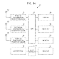
- FIG. 14 is a diagram illustrating an example of the wireless communication apparatus according to the embodiment.
- Cellular phones and smart phones are examples of the wireless communication apparatus.
- the wireless communication apparatus corresponds to a cellular phone or a smart phone.
- the wireless communication apparatus of this embodiment is applicable to wireless communication apparatuses other than cellular phones and smart phones.
- a wireless communication apparatus 51 includes a first radio frequency (RF) transmission/reception device 52, a second RF transmission/reception device 53, and a third RF transmission/reception device 54.
- the number of the FR transmission/reception devices may be one, two, four, or more.
- the wireless communication apparatus 51 includes a microphone 55, a central processing unit (CPU) 56, an audio circuit 57, a display 58, an input key 59, a memory 60, and a speaker 61.
- CPU central processing unit
- the first RF transmission/reception device 52 is coupled to an antenna 62 and the CPU 56.
- the antenna 62 may be the antenna 1 illustrated in FIG. 1 or FIG. 6 .
- the first RF transmission/reception device 52 receives a wireless signal from a mobile telephone network through the antenna 62, for example, generates reception data from the received signal, and transmits the reception data to the CPU 56.
- the first RF transmission/reception device 52 generates a transmission signal from transmission data supplied from the CPU 56 and transmits the transmission signal to the mobile telephone network through the antenna 62, for example.
- the second RF transmission/reception device 53 is connected to an antenna 63 and the CPU 56.
- the antenna 63 may be the antenna 1 illustrated in FIG. 1 or FIG. 6 .
- the second RF transmission/reception device 53 receives a wireless signal from a wireless local area network (LAN) through the antenna 63, for example, generates reception data from the received signal, and transmits the reception data to the CPU 56.
- the second RF transmission/reception device 53 generates a transmission signal from transmission data supplied from the CPU 56 and transmits the transmission signal to the wireless LAN through the antenna 63, for example.
- LAN wireless local area network
- the third RF transmission/reception device 54 is coupled to an antenna 64 and the CPU 56.
- the antenna 64 may be the antenna 1 illustrated in FIG. 1 or FIG. 6 .
- the third RF transmission/reception device 54 receives a wireless signal from a near field communication (NFC) network through the antenna 64, for example, generates reception data from the received signal, and transmits the reception data to the CPU 56.
- the third RF transmission/reception device 54 generates a transmission signal from transmission data supplied from the CPU 56 and transmits the transmission signal to the NFC network through the antenna 64, for example.
- NFC near field communication
- the wireless communication apparatus 51 may include an antenna and an RF reception device which receive electromagnetic waves of frequencies used for wireless chargers, digital terrestrial broadcasting, satellite broadcasting, or a global positioning system (GPS).
- the wireless communication apparatus 51 may include an antenna and an RF transmission/reception device which transmit and receive electromagnetic waves of frequencies used for FM transmitters and the Bluetooth (registered trademark).
- the display 58 is coupled to the CPU 56.
- the display 58 displays text and images in accordance with data output from the CPU 56.
- a touch panel may be disposed on a surface of the display 58 so that characters and symbols are input using the touch panel.
- the input key 59 is coupled to the CPU 56.
- the input key 59 is used to input characters and symbols to the CPU 56.
- the memory 60 is coupled to the CPU 56.
- the memory 60 stores programs of an operating system (OS) and various applications which are to be executed by the CPU 56.
- the memory 60 is used as a working area of the CPU 56.
- the speaker 61 is coupled to the audio circuit 57.
- the speaker 61 outputs audio in accordance with a signal output from the audio circuit 57.
- the microphone 55 is coupled to the audio circuit 57.
- the microphone 55 is used to input an audio signal to the audio circuit 57.
- the audio circuit 57 is coupled to the CPU 56.
- the audio circuit 57 generates audio data from an audio signal supplied from the microphone 55 and transmits the audio data to the CPU 56. Furthermore, the audio circuit 57 generates an audio signal from audio data supplied from the CPU 56 and transmits the audio signal to the speaker 61.
- the CPU 56 executes the programs of the operating system and the various applications.
- the CPU 56 processes data input from the first RF transmission/reception device 52, the second RF transmission/reception device 53, the third RF transmission/reception device 54, the input key 59, the memory 60, and the audio circuit 57.
- the CPU 56 outputs processed data to the first RF transmission/reception device 52, the second RF transmission/reception device 53, the third RF transmission/reception device 54, the display 58, the memory 60, and the audio circuit 57.
- the CPU 56 controls entire operation of the wireless communication apparatus 51.
- the wireless communication apparatus 51 may include a CPU used for wireless communication and a CPU used to execute application programs.
- FIG. 15 is a diagram illustrating arrangement of the antennas in the wireless communication apparatus 51 of FIG. 14 .
- FIG. 16 is a diagram illustrating the example of the arrangement of the antennas of FIG. 14 viewed from a side.
- antennas 74, 75, and 76 when antennas 74, 75, and 76 correspond to the antenna 1 illustrated in FIG. 1 or FIG. 6 , the antennas 74, 75, and 76 may be linearly implemented on plates 71, 72, and 73 having the ground potential so as not to be away from the plates 71, 72, and 73.
- reference numerals 77, 78, and 79 denote contact springs for the antennas 74, 75, and 76.
- FIG. 17 is a diagram illustrating an example of arrangement of antennas when the antennas of the embodiment are not used.
- FIG. 18 is a diagram illustrating an example of the arrangement of the antennas of FIG. 17 viewed from a side.
- antennas 84, 85, and 86 do not correspond to the antenna 1 illustrated in FIG. 1 or FIG. 6
- the antennas 84, 85, and 86 are implemented so as not to be arranged on plates 81, 82, and 83 and bypass the plates 81, 82, and 83.
- the antennas 84, 85, and 86 are implemented so as to be away from the plates 81, 82, and 83 having the ground potential.
- the antennas 84, 85, and 86 are implemented so as to be away from the plates 81, 82, and 83 having the ground potential by a distance h.
- the distance h is equal to or larger than 1 mm, for example.
- reference numerals 87, 88, and 89 denote contact springs for the antennas 84, 85, and 86.
- the wireless communication apparatus 51 since each of the antennas 74, 75, and 76 has an electric wall and a magnetic wall, the antennas 74, 75, and 76 may be linearly implemented on the plates 71, 72, and 73 so as not to be away from the plates 71, 72, and 73. Therefore, a dead space to be used by the antennas 74, 75, and 76 for bypassing the plates 71, 72, and 73 is not provided and a space for separating the antennas 74, 75, and 76 from the plates 71, 72, and 73 is not provided. Accordingly, the small and thin wireless communication apparatus 51 may be obtained.
- a thickness of the wireless communication apparatus 51 may be reduced by 1 mm or more, for example, when compared with the wireless communication apparatus corresponding to the antenna arrangement example illustrated in FIGs. 17 and 18 .
- use of the antenna 1 illustrated in FIG. 1 or FIG. 6 may omit the via holes included in the mushroom structure. Accordingly, a thinner wireless communication apparatus may be obtained when compared with the case where the antenna having the electromagnetic wall having the mushroom structure is used.
Landscapes
- Details Of Aerials (AREA)
- Aerials With Secondary Devices (AREA)
- Transceivers (AREA)
Applications Claiming Priority (1)
| Application Number | Priority Date | Filing Date | Title |
|---|---|---|---|
| JP2013075083A JP2014200031A (ja) | 2013-03-29 | 2013-03-29 | アンテナ及び無線通信装置 |
Publications (2)
| Publication Number | Publication Date |
|---|---|
| EP2784875A1 true EP2784875A1 (fr) | 2014-10-01 |
| EP2784875B1 EP2784875B1 (fr) | 2016-03-16 |
Family
ID=50289590
Family Applications (1)
| Application Number | Title | Priority Date | Filing Date |
|---|---|---|---|
| EP14160912.3A Not-in-force EP2784875B1 (fr) | 2013-03-29 | 2014-03-20 | Antenne et appareil de communication sans fil |
Country Status (3)
| Country | Link |
|---|---|
| US (1) | US20140292600A1 (fr) |
| EP (1) | EP2784875B1 (fr) |
| JP (1) | JP2014200031A (fr) |
Families Citing this family (3)
| Publication number | Priority date | Publication date | Assignee | Title |
|---|---|---|---|---|
| KR102605856B1 (ko) * | 2017-01-03 | 2023-11-24 | 주식회사 위츠 | 안테나 장치 및 이를 구비하는 휴대 단말기 |
| JP7141110B2 (ja) * | 2019-06-06 | 2022-09-22 | 国立研究開発法人宇宙航空研究開発機構 | メタマテリアルアンテナ |
| CN116937177B (zh) * | 2023-07-13 | 2024-04-26 | 苏州铂韬新材料科技有限公司 | 一种手机nfc天线及其吸波材料的制备方法 |
Citations (4)
| Publication number | Priority date | Publication date | Assignee | Title |
|---|---|---|---|---|
| US20090174609A1 (en) * | 2006-07-14 | 2009-07-09 | Yamaguchi University | Stripline-type composite right/left-handed transmission line or left-handed transmission line, and antenna that uses same |
| WO2010013496A1 (fr) | 2008-08-01 | 2010-02-04 | 日本電気株式会社 | Structure, carte de circuit imprimé, antenne, convertisseur de longueur d'onde de ligne de transmission, antenne en réseau et dispositif électronique |
| JP2011055054A (ja) | 2009-08-31 | 2011-03-17 | Mitsubishi Electric Corp | 磁気壁基板および磁気壁基板を用いたアンテナシステム |
| WO2012108351A1 (fr) * | 2011-02-10 | 2012-08-16 | 株式会社村田製作所 | Métamatériau, appareil électrique et appareil électrique équipé d'un métamatériau |
Family Cites Families (16)
| Publication number | Priority date | Publication date | Assignee | Title |
|---|---|---|---|---|
| AU9261598A (en) * | 1997-08-08 | 1999-03-01 | Ird A/S | Polymeric radio frequency resonant tags and method for manufacture |
| WO2001071774A2 (fr) * | 2000-03-17 | 2001-09-27 | The Regents Of The University Of California | Milieu composite polarisé à gauche |
| WO2003030298A1 (fr) * | 2001-08-23 | 2003-04-10 | Broadcom Corporation | Dispositif de formation d'interfaces magnetiques et applications afferentes |
| US6774866B2 (en) * | 2002-06-14 | 2004-08-10 | Etenna Corporation | Multiband artificial magnetic conductor |
| US8271241B2 (en) * | 2005-01-18 | 2012-09-18 | University Of Massachusetts Lowell | Chiral metamaterials |
| JP2006253929A (ja) * | 2005-03-09 | 2006-09-21 | Mitsubishi Electric Corp | Ebgマテリアル |
| US7629931B2 (en) * | 2005-04-15 | 2009-12-08 | Nokia Corporation | Antenna having a plurality of resonant frequencies |
| JP2007243559A (ja) * | 2006-03-08 | 2007-09-20 | Mitsumi Electric Co Ltd | アンテナモジュール及びアンテナ装置 |
| US7492329B2 (en) * | 2006-10-12 | 2009-02-17 | Hewlett-Packard Development Company, L.P. | Composite material with chirped resonant cells |
| JP5380919B2 (ja) * | 2008-06-24 | 2014-01-08 | 日本電気株式会社 | 導波路構造およびプリント配線板 |
| US9570814B2 (en) * | 2008-09-11 | 2017-02-14 | Nec Corporation | Structure, antenna, communication device and electronic component |
| JP5336873B2 (ja) * | 2009-02-09 | 2013-11-06 | Necトーキン株式会社 | 高表面インピーダンス構造体、アンテナ装置、及びrfidタグ |
| WO2010116675A1 (fr) * | 2009-03-30 | 2010-10-14 | 日本電気株式会社 | Antenne de résonateur |
| WO2010125784A1 (fr) * | 2009-04-30 | 2010-11-04 | 日本電気株式会社 | Corps structurel, carte de circuit imprimé, antenne, convertisseur guide d'ondes de ligne de transmission, antenne réseau, et dispositif électronique |
| CN102792519A (zh) * | 2010-03-08 | 2012-11-21 | 日本电气株式会社 | 结构、线路板和制造线路板的方法 |
| WO2011152055A1 (fr) * | 2010-06-02 | 2011-12-08 | 日本電気株式会社 | Corps structuré |
-
2013
- 2013-03-29 JP JP2013075083A patent/JP2014200031A/ja active Pending
-
2014
- 2014-03-13 US US14/209,373 patent/US20140292600A1/en not_active Abandoned
- 2014-03-20 EP EP14160912.3A patent/EP2784875B1/fr not_active Not-in-force
Patent Citations (5)
| Publication number | Priority date | Publication date | Assignee | Title |
|---|---|---|---|---|
| US20090174609A1 (en) * | 2006-07-14 | 2009-07-09 | Yamaguchi University | Stripline-type composite right/left-handed transmission line or left-handed transmission line, and antenna that uses same |
| WO2010013496A1 (fr) | 2008-08-01 | 2010-02-04 | 日本電気株式会社 | Structure, carte de circuit imprimé, antenne, convertisseur de longueur d'onde de ligne de transmission, antenne en réseau et dispositif électronique |
| US20110134010A1 (en) * | 2008-08-01 | 2011-06-09 | Nec Corporation | Structure, printed circuit board, antenna, transmission line to waveguide converter, array antenna, and electronic device |
| JP2011055054A (ja) | 2009-08-31 | 2011-03-17 | Mitsubishi Electric Corp | 磁気壁基板および磁気壁基板を用いたアンテナシステム |
| WO2012108351A1 (fr) * | 2011-02-10 | 2012-08-16 | 株式会社村田製作所 | Métamatériau, appareil électrique et appareil électrique équipé d'un métamatériau |
Non-Patent Citations (9)
| Title |
|---|
| D. R. SMITH ET AL.: "Electromagnetic Parameter Retrieval from Inhomogeneous Metamaterials", PHYSICAL REVIEW, vol. E71, 2005, pages 036617 - 1,036617-11 |
| KATAYAMA NAOKI ET AL.: "Estimation for Material Parameters of Metamaterial by Using Complex Chart Procedure", PROCEEDINGS OF IEEE HIROSHIMA STUDENT SYMPOSIUM, vol. 10, 2008, pages 86 - 89 |
| KATAYAMA NAOKI ET AL.: "Estimation for Material Parameters of Metamaterial by Using Complex Chart Procedure", PROCEEDINGS OF.TEEE HIROSHIMA STUDENT SYMPOSIUM, vol. 10, 2008, pages 86 - 89 |
| MATSUNAGA NAOKO ET AL.: "On a Novel Two-Dimensional Planer Distributed Structure with Negative Refractive Index", THE 2005 IEICE GENERAL CONFERENCE, vol. CS-2-3, pages S22 - S23 |
| NAKANO HISAMATSU: "Applications of Metamaterials to Antennas", THE 2006 IEICE GENERAL CONFERENCE, vol. BT-1-2, pages SS40 - SS41 |
| SANADA ATSUSHI, WHAT IS METAMATERIALS, 12 January 2009 (2009-01-12), pages 104 - 111 |
| SANADA ATSUSHI, WHAT IS METAMATERIALS, 15 December 2008 (2008-12-15), pages 159 - 169 |
| SANADA ATSUSHI, WHAT IS METAMATERIALS, 17 November 2008 (2008-11-17), pages 128 - 134 |
| SANADA ATSUSHI, WHAT IS METAMATERIALS, 9 February 2009 (2009-02-09), pages 110 - 116 |
Also Published As
| Publication number | Publication date |
|---|---|
| JP2014200031A (ja) | 2014-10-23 |
| US20140292600A1 (en) | 2014-10-02 |
| EP2784875B1 (fr) | 2016-03-16 |
Similar Documents
| Publication | Publication Date | Title |
|---|---|---|
| KR102233837B1 (ko) | 통신 및 레인징 능력들을 갖는 전자 디바이스들 | |
| US11641061B2 (en) | Millimeter wave patch antennas | |
| Sharawi et al. | A CSRR loaded MIMO antenna system for ISM band operation | |
| US10608321B2 (en) | Antennas in patterned conductive layers | |
| US10879592B2 (en) | Vertical antenna patch in cavity region | |
| EP3883061B1 (fr) | Dispositif d'antenne et terminal | |
| EP3025392B1 (fr) | Antenne à bande électromagnétique interdite dépendant de la polarisation et procédés associés | |
| US8624788B2 (en) | Antenna assembly utilizing metal-dielectric resonant structures for specific absorption rate compliance | |
| CN111129704B (zh) | 一种天线单元和电子设备 | |
| US8786507B2 (en) | Antenna assembly utilizing metal-dielectric structures | |
| JP2015185946A (ja) | アンテナ装置 | |
| CN107706529A (zh) | 一种去耦组件、多天线系统及终端 | |
| KR102742799B1 (ko) | 콤팩트한 초광대역 안테나 모듈들을 갖는 전자 디바이스들 | |
| WO2008128582A1 (fr) | Eléments de connexion électrique disposés dans la structure amc d'un agencement d'antenne | |
| CN109478721A (zh) | 形成在多层印刷电路板边缘上的c馈电天线 | |
| WO2017114024A1 (fr) | Antenne à double polarisation et dispositif de communication | |
| WO2015001181A1 (fr) | Appareil et procédés pour une communication sans fil | |
| EP2784875B1 (fr) | Antenne et appareil de communication sans fil | |
| EP2518823B1 (fr) | Ensemble formant antenne utilisant des structures résonantes diélectriques métalliques pour conformité à un taux d'absorption spécifique | |
| KR20230084051A (ko) | 틸팅된 안테나 어레이들을 갖는 전자 디바이스들 | |
| Shakir et al. | A compact 8-element 3D UWB diversity antenna system for off device installation | |
| CN110808455B (zh) | 一种天线单元及电子设备 | |
| JP7753446B2 (ja) | 再帰性反射構造を含む通信デバイス | |
| US20110240744A1 (en) | Antenna substrate and rfid tag | |
| CN107645038B (zh) | 一种天线及移动终端 |
Legal Events
| Date | Code | Title | Description |
|---|---|---|---|
| 17P | Request for examination filed |
Effective date: 20140320 |
|
| AK | Designated contracting states |
Kind code of ref document: A1 Designated state(s): AL AT BE BG CH CY CZ DE DK EE ES FI FR GB GR HR HU IE IS IT LI LT LU LV MC MK MT NL NO PL PT RO RS SE SI SK SM TR |
|
| AX | Request for extension of the european patent |
Extension state: BA ME |
|
| PUAI | Public reference made under article 153(3) epc to a published international application that has entered the european phase |
Free format text: ORIGINAL CODE: 0009012 |
|
| R17P | Request for examination filed (corrected) |
Effective date: 20150112 |
|
| RBV | Designated contracting states (corrected) |
Designated state(s): AL AT BE BG CH CY CZ DE DK EE ES FI FR GB GR HR HU IE IS IT LI LT LU LV MC MK MT NL NO PL PT RO RS SE SI SK SM TR |
|
| REG | Reference to a national code |
Ref country code: DE Ref legal event code: R079 Ref document number: 602014001074 Country of ref document: DE Free format text: PREVIOUS MAIN CLASS: H01Q0015000000 Ipc: H01Q0001360000 |
|
| RIC1 | Information provided on ipc code assigned before grant |
Ipc: H01Q 1/36 20060101AFI20150827BHEP Ipc: H01Q 15/00 20060101ALI20150827BHEP |
|
| GRAP | Despatch of communication of intention to grant a patent |
Free format text: ORIGINAL CODE: EPIDOSNIGR1 |
|
| INTG | Intention to grant announced |
Effective date: 20151002 |
|
| GRAS | Grant fee paid |
Free format text: ORIGINAL CODE: EPIDOSNIGR3 |
|
| GRAA | (expected) grant |
Free format text: ORIGINAL CODE: 0009210 |
|
| AK | Designated contracting states |
Kind code of ref document: B1 Designated state(s): AL AT BE BG CH CY CZ DE DK EE ES FI FR GB GR HR HU IE IS IT LI LT LU LV MC MK MT NL NO PL PT RO RS SE SI SK SM TR |
|
| REG | Reference to a national code |
Ref country code: GB Ref legal event code: FG4D |
|
| REG | Reference to a national code |
Ref country code: FR Ref legal event code: PLFP Year of fee payment: 3 |
|
| REG | Reference to a national code |
Ref country code: CH Ref legal event code: EP |
|
| REG | Reference to a national code |
Ref country code: IE Ref legal event code: FG4D |
|
| REG | Reference to a national code |
Ref country code: AT Ref legal event code: REF Ref document number: 781928 Country of ref document: AT Kind code of ref document: T Effective date: 20160415 |
|
| REG | Reference to a national code |
Ref country code: DE Ref legal event code: R096 Ref document number: 602014001074 Country of ref document: DE |
|
| REG | Reference to a national code |
Ref country code: NL Ref legal event code: MP Effective date: 20160316 |
|
| REG | Reference to a national code |
Ref country code: LT Ref legal event code: MG4D |
|
| PG25 | Lapsed in a contracting state [announced via postgrant information from national office to epo] |
Ref country code: FI Free format text: LAPSE BECAUSE OF FAILURE TO SUBMIT A TRANSLATION OF THE DESCRIPTION OR TO PAY THE FEE WITHIN THE PRESCRIBED TIME-LIMIT Effective date: 20160316 Ref country code: HR Free format text: LAPSE BECAUSE OF FAILURE TO SUBMIT A TRANSLATION OF THE DESCRIPTION OR TO PAY THE FEE WITHIN THE PRESCRIBED TIME-LIMIT Effective date: 20160316 Ref country code: NO Free format text: LAPSE BECAUSE OF FAILURE TO SUBMIT A TRANSLATION OF THE DESCRIPTION OR TO PAY THE FEE WITHIN THE PRESCRIBED TIME-LIMIT Effective date: 20160616 Ref country code: GR Free format text: LAPSE BECAUSE OF FAILURE TO SUBMIT A TRANSLATION OF THE DESCRIPTION OR TO PAY THE FEE WITHIN THE PRESCRIBED TIME-LIMIT Effective date: 20160617 |
|
| REG | Reference to a national code |
Ref country code: AT Ref legal event code: MK05 Ref document number: 781928 Country of ref document: AT Kind code of ref document: T Effective date: 20160316 |
|
| PG25 | Lapsed in a contracting state [announced via postgrant information from national office to epo] |
Ref country code: RS Free format text: LAPSE BECAUSE OF FAILURE TO SUBMIT A TRANSLATION OF THE DESCRIPTION OR TO PAY THE FEE WITHIN THE PRESCRIBED TIME-LIMIT Effective date: 20160316 Ref country code: NL Free format text: LAPSE BECAUSE OF FAILURE TO SUBMIT A TRANSLATION OF THE DESCRIPTION OR TO PAY THE FEE WITHIN THE PRESCRIBED TIME-LIMIT Effective date: 20160316 Ref country code: LV Free format text: LAPSE BECAUSE OF FAILURE TO SUBMIT A TRANSLATION OF THE DESCRIPTION OR TO PAY THE FEE WITHIN THE PRESCRIBED TIME-LIMIT Effective date: 20160316 Ref country code: SE Free format text: LAPSE BECAUSE OF FAILURE TO SUBMIT A TRANSLATION OF THE DESCRIPTION OR TO PAY THE FEE WITHIN THE PRESCRIBED TIME-LIMIT Effective date: 20160316 Ref country code: BE Free format text: LAPSE BECAUSE OF NON-PAYMENT OF DUE FEES Effective date: 20160331 Ref country code: LT Free format text: LAPSE BECAUSE OF FAILURE TO SUBMIT A TRANSLATION OF THE DESCRIPTION OR TO PAY THE FEE WITHIN THE PRESCRIBED TIME-LIMIT Effective date: 20160316 |
|
| PG25 | Lapsed in a contracting state [announced via postgrant information from national office to epo] |
Ref country code: PL Free format text: LAPSE BECAUSE OF FAILURE TO SUBMIT A TRANSLATION OF THE DESCRIPTION OR TO PAY THE FEE WITHIN THE PRESCRIBED TIME-LIMIT Effective date: 20160316 Ref country code: IS Free format text: LAPSE BECAUSE OF FAILURE TO SUBMIT A TRANSLATION OF THE DESCRIPTION OR TO PAY THE FEE WITHIN THE PRESCRIBED TIME-LIMIT Effective date: 20160716 Ref country code: EE Free format text: LAPSE BECAUSE OF FAILURE TO SUBMIT A TRANSLATION OF THE DESCRIPTION OR TO PAY THE FEE WITHIN THE PRESCRIBED TIME-LIMIT Effective date: 20160316 |
|
| PG25 | Lapsed in a contracting state [announced via postgrant information from national office to epo] |
Ref country code: ES Free format text: LAPSE BECAUSE OF FAILURE TO SUBMIT A TRANSLATION OF THE DESCRIPTION OR TO PAY THE FEE WITHIN THE PRESCRIBED TIME-LIMIT Effective date: 20160316 Ref country code: RO Free format text: LAPSE BECAUSE OF FAILURE TO SUBMIT A TRANSLATION OF THE DESCRIPTION OR TO PAY THE FEE WITHIN THE PRESCRIBED TIME-LIMIT Effective date: 20160316 Ref country code: AT Free format text: LAPSE BECAUSE OF FAILURE TO SUBMIT A TRANSLATION OF THE DESCRIPTION OR TO PAY THE FEE WITHIN THE PRESCRIBED TIME-LIMIT Effective date: 20160316 Ref country code: PT Free format text: LAPSE BECAUSE OF FAILURE TO SUBMIT A TRANSLATION OF THE DESCRIPTION OR TO PAY THE FEE WITHIN THE PRESCRIBED TIME-LIMIT Effective date: 20160718 Ref country code: CZ Free format text: LAPSE BECAUSE OF FAILURE TO SUBMIT A TRANSLATION OF THE DESCRIPTION OR TO PAY THE FEE WITHIN THE PRESCRIBED TIME-LIMIT Effective date: 20160316 Ref country code: SK Free format text: LAPSE BECAUSE OF FAILURE TO SUBMIT A TRANSLATION OF THE DESCRIPTION OR TO PAY THE FEE WITHIN THE PRESCRIBED TIME-LIMIT Effective date: 20160316 Ref country code: SM Free format text: LAPSE BECAUSE OF FAILURE TO SUBMIT A TRANSLATION OF THE DESCRIPTION OR TO PAY THE FEE WITHIN THE PRESCRIBED TIME-LIMIT Effective date: 20160316 |
|
| REG | Reference to a national code |
Ref country code: DE Ref legal event code: R097 Ref document number: 602014001074 Country of ref document: DE |
|
| REG | Reference to a national code |
Ref country code: IE Ref legal event code: MM4A |
|
| PG25 | Lapsed in a contracting state [announced via postgrant information from national office to epo] |
Ref country code: BE Free format text: LAPSE BECAUSE OF FAILURE TO SUBMIT A TRANSLATION OF THE DESCRIPTION OR TO PAY THE FEE WITHIN THE PRESCRIBED TIME-LIMIT Effective date: 20160316 |
|
| PLBE | No opposition filed within time limit |
Free format text: ORIGINAL CODE: 0009261 |
|
| STAA | Information on the status of an ep patent application or granted ep patent |
Free format text: STATUS: NO OPPOSITION FILED WITHIN TIME LIMIT |
|
| PG25 | Lapsed in a contracting state [announced via postgrant information from national office to epo] |
Ref country code: IE Free format text: LAPSE BECAUSE OF NON-PAYMENT OF DUE FEES Effective date: 20160320 Ref country code: DK Free format text: LAPSE BECAUSE OF FAILURE TO SUBMIT A TRANSLATION OF THE DESCRIPTION OR TO PAY THE FEE WITHIN THE PRESCRIBED TIME-LIMIT Effective date: 20160316 |
|
| REG | Reference to a national code |
Ref country code: FR Ref legal event code: PLFP Year of fee payment: 4 |
|
| 26N | No opposition filed |
Effective date: 20161219 |
|
| PG25 | Lapsed in a contracting state [announced via postgrant information from national office to epo] |
Ref country code: BG Free format text: LAPSE BECAUSE OF FAILURE TO SUBMIT A TRANSLATION OF THE DESCRIPTION OR TO PAY THE FEE WITHIN THE PRESCRIBED TIME-LIMIT Effective date: 20160616 |
|
| PGFP | Annual fee paid to national office [announced via postgrant information from national office to epo] |
Ref country code: DE Payment date: 20170314 Year of fee payment: 4 Ref country code: FR Payment date: 20170213 Year of fee payment: 4 |
|
| PG25 | Lapsed in a contracting state [announced via postgrant information from national office to epo] |
Ref country code: SI Free format text: LAPSE BECAUSE OF FAILURE TO SUBMIT A TRANSLATION OF THE DESCRIPTION OR TO PAY THE FEE WITHIN THE PRESCRIBED TIME-LIMIT Effective date: 20160316 |
|
| PG25 | Lapsed in a contracting state [announced via postgrant information from national office to epo] |
Ref country code: IT Free format text: LAPSE BECAUSE OF FAILURE TO SUBMIT A TRANSLATION OF THE DESCRIPTION OR TO PAY THE FEE WITHIN THE PRESCRIBED TIME-LIMIT Effective date: 20160316 |
|
| PG25 | Lapsed in a contracting state [announced via postgrant information from national office to epo] |
Ref country code: MT Free format text: LAPSE BECAUSE OF FAILURE TO SUBMIT A TRANSLATION OF THE DESCRIPTION OR TO PAY THE FEE WITHIN THE PRESCRIBED TIME-LIMIT Effective date: 20160316 |
|
| REG | Reference to a national code |
Ref country code: CH Ref legal event code: PL |
|
| PG25 | Lapsed in a contracting state [announced via postgrant information from national office to epo] |
Ref country code: CH Free format text: LAPSE BECAUSE OF NON-PAYMENT OF DUE FEES Effective date: 20170331 Ref country code: LI Free format text: LAPSE BECAUSE OF NON-PAYMENT OF DUE FEES Effective date: 20170331 |
|
| PGFP | Annual fee paid to national office [announced via postgrant information from national office to epo] |
Ref country code: GB Payment date: 20180103 Year of fee payment: 5 |
|
| PG25 | Lapsed in a contracting state [announced via postgrant information from national office to epo] |
Ref country code: HU Free format text: LAPSE BECAUSE OF FAILURE TO SUBMIT A TRANSLATION OF THE DESCRIPTION OR TO PAY THE FEE WITHIN THE PRESCRIBED TIME-LIMIT; INVALID AB INITIO Effective date: 20140320 |
|
| PG25 | Lapsed in a contracting state [announced via postgrant information from national office to epo] |
Ref country code: MC Free format text: LAPSE BECAUSE OF FAILURE TO SUBMIT A TRANSLATION OF THE DESCRIPTION OR TO PAY THE FEE WITHIN THE PRESCRIBED TIME-LIMIT Effective date: 20160316 Ref country code: MT Free format text: LAPSE BECAUSE OF FAILURE TO SUBMIT A TRANSLATION OF THE DESCRIPTION OR TO PAY THE FEE WITHIN THE PRESCRIBED TIME-LIMIT Effective date: 20160331 Ref country code: LU Free format text: LAPSE BECAUSE OF NON-PAYMENT OF DUE FEES Effective date: 20160320 Ref country code: MK Free format text: LAPSE BECAUSE OF FAILURE TO SUBMIT A TRANSLATION OF THE DESCRIPTION OR TO PAY THE FEE WITHIN THE PRESCRIBED TIME-LIMIT Effective date: 20160316 Ref country code: CY Free format text: LAPSE BECAUSE OF FAILURE TO SUBMIT A TRANSLATION OF THE DESCRIPTION OR TO PAY THE FEE WITHIN THE PRESCRIBED TIME-LIMIT Effective date: 20160316 Ref country code: TR Free format text: LAPSE BECAUSE OF FAILURE TO SUBMIT A TRANSLATION OF THE DESCRIPTION OR TO PAY THE FEE WITHIN THE PRESCRIBED TIME-LIMIT Effective date: 20160316 |
|
| REG | Reference to a national code |
Ref country code: DE Ref legal event code: R119 Ref document number: 602014001074 Country of ref document: DE |
|
| PG25 | Lapsed in a contracting state [announced via postgrant information from national office to epo] |
Ref country code: AL Free format text: LAPSE BECAUSE OF FAILURE TO SUBMIT A TRANSLATION OF THE DESCRIPTION OR TO PAY THE FEE WITHIN THE PRESCRIBED TIME-LIMIT Effective date: 20160316 |
|
| PG25 | Lapsed in a contracting state [announced via postgrant information from national office to epo] |
Ref country code: DE Free format text: LAPSE BECAUSE OF NON-PAYMENT OF DUE FEES Effective date: 20181002 |
|
| PG25 | Lapsed in a contracting state [announced via postgrant information from national office to epo] |
Ref country code: FR Free format text: LAPSE BECAUSE OF NON-PAYMENT OF DUE FEES Effective date: 20180331 |
|
| GBPC | Gb: european patent ceased through non-payment of renewal fee |
Effective date: 20190320 |
|
| PG25 | Lapsed in a contracting state [announced via postgrant information from national office to epo] |
Ref country code: GB Free format text: LAPSE BECAUSE OF NON-PAYMENT OF DUE FEES Effective date: 20190320 |