WO2012108351A1 - Métamatériau, appareil électrique et appareil électrique équipé d'un métamatériau - Google Patents
Métamatériau, appareil électrique et appareil électrique équipé d'un métamatériau Download PDFInfo
- Publication number
- WO2012108351A1 WO2012108351A1 PCT/JP2012/052498 JP2012052498W WO2012108351A1 WO 2012108351 A1 WO2012108351 A1 WO 2012108351A1 JP 2012052498 W JP2012052498 W JP 2012052498W WO 2012108351 A1 WO2012108351 A1 WO 2012108351A1
- Authority
- WO
- WIPO (PCT)
- Prior art keywords
- metamaterial
- region
- antenna
- specific region
- electrode
- Prior art date
- Legal status (The legal status is an assumption and is not a legal conclusion. Google has not performed a legal analysis and makes no representation as to the accuracy of the status listed.)
- Ceased
Links
Images


Classifications
-
- H—ELECTRICITY
- H01—ELECTRIC ELEMENTS
- H01Q—ANTENNAS, i.e. RADIO AERIALS
- H01Q1/00—Details of, or arrangements associated with, antennas
- H01Q1/36—Structural form of radiating elements, e.g. cone, spiral, umbrella; Particular materials used therewith
-
- H—ELECTRICITY
- H01—ELECTRIC ELEMENTS
- H01Q—ANTENNAS, i.e. RADIO AERIALS
- H01Q1/00—Details of, or arrangements associated with, antennas
- H01Q1/12—Supports; Mounting means
- H01Q1/22—Supports; Mounting means by structural association with other equipment or articles
- H01Q1/24—Supports; Mounting means by structural association with other equipment or articles with receiving set
- H01Q1/241—Supports; Mounting means by structural association with other equipment or articles with receiving set used in mobile communications, e.g. GSM
- H01Q1/242—Supports; Mounting means by structural association with other equipment or articles with receiving set used in mobile communications, e.g. GSM specially adapted for hand-held use
- H01Q1/243—Supports; Mounting means by structural association with other equipment or articles with receiving set used in mobile communications, e.g. GSM specially adapted for hand-held use with built-in antennas
-
- H—ELECTRICITY
- H01—ELECTRIC ELEMENTS
- H01Q—ANTENNAS, i.e. RADIO AERIALS
- H01Q13/00—Waveguide horns or mouths; Slot antennas; Leaky-waveguide antennas; Equivalent structures causing radiation along the transmission path of a guided wave
- H01Q13/08—Radiating ends of two-conductor microwave transmission lines, e.g. of coaxial lines, of microstrip lines
-
- H—ELECTRICITY
- H01—ELECTRIC ELEMENTS
- H01Q—ANTENNAS, i.e. RADIO AERIALS
- H01Q15/00—Devices for reflection, refraction, diffraction or polarisation of waves radiated from an antenna, e.g. quasi-optical devices
- H01Q15/0006—Devices acting selectively as reflecting surface, as diffracting or as refracting device, e.g. frequency filtering or angular spatial filtering devices
- H01Q15/0086—Devices acting selectively as reflecting surface, as diffracting or as refracting device, e.g. frequency filtering or angular spatial filtering devices said selective devices having materials with a synthesized negative refractive index, e.g. metamaterials or left-handed materials
-
- H—ELECTRICITY
- H04—ELECTRIC COMMUNICATION TECHNIQUE
- H04M—TELEPHONIC COMMUNICATION
- H04M1/00—Substation equipment, e.g. for use by subscribers
- H04M1/02—Constructional features of telephone sets
- H04M1/0202—Portable telephone sets, e.g. cordless phones, mobile phones or bar type handsets
Definitions
- the present invention relates to a metamaterial, an electric device, and an electric device provided with the metamaterial.
- a normal antenna is configured by forming a line having a length of ⁇ / 4 into a bar or plate shape, or forming a conductor on a film or a printed board.
- Patent Document 1 Japanese Patent Laid-Open No. 9-162625
- Patent Document 2 a structure called a mushroom structure with a slit in the surface has been proposed (for example, JP 2009-535942 A (hereinafter referred to as “Patent Document 2”) and JP 2010-502131 A. Gazette (hereinafter referred to as “Patent Document 3”).
- a 1-segment partial reception service for mobile phones / mobile terminals a so-called mono-segment antenna for receiving one-segment broadcasting, is provided outside the device as a telescopic rod type.
- the antenna of a mobile phone is often configured on a printed circuit board.
- the chip antenna is mounted on the substrate.
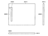
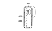
- FIG. 75 is a diagram showing the arrangement of the conventional antenna 3000 when the case 3001 is made of resin.
- antenna 3000 when antenna 3000 is formed on a substrate 3300 such as a cellular phone, there is no problem because radio waves can be transmitted if case 3001 outside the cellular phone is made of resin.
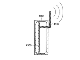
- FIG. 76 is a diagram showing a case where the case 4001 is made of metal. Referring to FIG. 76, when case 4001 is made of metal or conductive resin, it does not transmit radio waves. Therefore, even if antenna 4000 is formed on internal substrate 4300, it functions as antenna 4000. I can't.
- the antennas described in Patent Document 1 to Patent Document 3 described above cannot function as an antenna when formed inside a case that does not transmit radio waves.
- FIG. 77 is a diagram showing a case where a part of the case 4002 of the metal case 4001 is formed of resin.
- the case 4001 does not transmit radio waves
- a portion of the case 4002 of the metal case 4001 is made of resin that transmits radio waves so that the radio waves are not blocked.
- a part of a metal top plate is made of resin, and an antenna is formed there.
- FIG. 78 is a diagram showing a case where the antenna 4100 is arranged outside the metal case 4001. Referring to FIG. 78, when case 4001 does not transmit radio waves, as a second method, antenna 4100 is provided outside the device.
- the antenna 4100 is attached to the outside of the device, there is no problem in the function of the antenna 4100. However, in that case, there is a problem that the antenna 4100 does not meet the needs of consumers because the antenna 4100 may be in the way or it may be troublesome to put out the antenna 4100. For this reason, a built-in antenna is still desired.
- the antenna since the portion to be replaced with resin can be minimized, the antenna must be mounted in a narrow space, and a small antenna is required, which may sacrifice the gain. Furthermore, as many wireless standards are developed, the required number of antennas is increasing, and the mounting positions of antennas are becoming insufficient.
- the separated part can function as an antenna, so the above-mentioned problems are solved.
- the present invention has been made to solve the above-described problems, and one of the objects of the present invention is to provide a metamaterial and an electric device capable of electromagnetically separating a specific area from other areas. It is to be.
- the metamaterial has a dielectric constant having an absolute value less than 1 and a permeability having an absolute value greater than 1 for a predetermined resonance wavelength of the electromagnetic field.
- a component in the vicinity of the resonance wavelength of the current that can be expressed and that flows through the conductive layer of a component having a conductive layer in a certain range in the depth direction for example, a metal layer only, a metal layer less than the skin depth + an insulator layer
- the blocking area (for example, high impedance area, reflection area) to be blocked is arranged to form a specific area of the conductive layer in a partition area that separates the other area, and at least a part of the specific area can radiate electromagnetic waves It is.
- the certain range in the depth direction of the component means a range in which the depth from one surface of the component is, for example, a to b (0 ⁇ a ⁇ b ⁇ t where the thickness of the component is t).
- the conductive layer occupies the entire range of component thickness.
- the conductive layer occupies a range from one side of the component to the depth b.
- the conductive layer occupies a range sandwiched between a layer from one side of the component to the depth a and a layer from the other side to the depth tb.
- the conductive layer occupies a range from the other surface of the component to the depth ta.
- the conductive layer has a thickness less than the skin depth according to the material of the conductive layer.
- a portion capable of emitting an electromagnetic wave in a specific region is formed on the surface of the conductive layer in the specific region.
- the specific area is in contact with the contour of the component (the edge of the component, if a slit is provided, the contour of the slit).
- the portion of the specific region that can emit electromagnetic waves is the end surface of the conductive layer in the specific region in contact with the contour of the component (for example, the end surface of the conductive layer exposed at the slit provided in contact with the specific region, the end of the component.
- the electric device includes a component having a conductive layer in a certain range in the depth direction (for example, only a metal layer, a metal layer less than the skin depth + insulator layer).
- the conductive layer includes a region that electromagnetically blocks a specific region of the conductive layer from other regions.
- the electric device further includes a metamaterial capable of exhibiting a dielectric constant having an absolute value of less than 1 and a magnetic permeability having an absolute value exceeding 1 with respect to a predetermined resonance wavelength of the electromagnetic field.
- the metamaterial is arranged so that a blocking region (for example, a high impedance region, a reflection region) that blocks a component near the resonance wavelength of the current flowing through the conductive layer is formed in a partition region that partitions the specific region from other regions.
- the At least a part of the specific region can emit electromagnetic waves.
- the certain range in the depth direction of the component means a range in which the depth from one surface of the component is, for example, a to b (0 ⁇ a ⁇ b ⁇ t where the thickness of the component is t).
- the conductive layer occupies the entire range of component thickness.
- the conductive layer occupies a range from one side of the component to the depth b.
- the conductive layer occupies a range sandwiched between a layer from one side of the component to the depth a and a layer from the other side to the depth tb.
- the conductive layer occupies a range from the other surface of the component to the depth ta.
- the conductive layer has a thickness less than the skin depth according to the material of the conductive layer.
- a portion capable of emitting an electromagnetic wave in a specific region is formed on the surface of the conductive layer in the specific region.
- the specific area is in contact with the contour of the component (the edge of the component, or the contour of the slit if a slit is provided).
- the portion of the specific region that can emit electromagnetic waves is the end surface of the conductive layer in the specific region in contact with the contour of the component (for example, the end surface of the conductive layer exposed at the slit provided in contact with the specific region, the end of the component The end surface of the conductive layer in a specific region provided on the substrate.
- a feeding point is provided in the specific area.
- the current flowing through the conductive layer is a current fed from a feeding point.
- the specific area is an antenna fed from a feeding point.
- the component constitutes a part of a casing molded so as to shield the inside from the outside.
- the metamaterial is provided inside the housing.
- the circuit further includes a circuit (for example, a tuning circuit, an amplifier circuit, an output circuit, etc.) that is provided inside the housing and supplies power to the feeding point and processes electromagnetic waves in the vicinity of the resonance wavelength that resonates in a specific region.
- the electric device further includes a grounding component disposed on the opposite side of the specific region with the metamaterial interposed therebetween.
- the electric device further includes a grounding part provided in place of the metamaterial in a part near the feeding point of the partition area.
- the electric device further includes a predetermined function unit (such as a camera unit) having a predetermined function (such as a camera function).
- a predetermined function unit such as a camera unit
- a predetermined function such as a camera function
- the metamaterial is preliminarily incorporated in the predetermined function unit so that the metamaterial is disposed at a position where the blocking region is formed in the partition region by attaching the predetermined function unit to the predetermined position.
- electromagnetic waves are incident on one surface of the specific region.
- the current flowing through the conductive layer is a current generated by an electromagnetic wave incident on one surface of the specific region.
- the specific region radiates an electromagnetic wave having the wavelength of the incident electromagnetic wave from the other surface.
- the metamaterial is composed of a multilayer ceramic capacitor or a chip coil.
- the specific area is an area in which a part of the part is partitioned by at least one of a slit and a grounding portion. At least a part of the specific region can emit electromagnetic waves.
- the specific area of the component functions as an antenna.
- part of the component having the conductive layer can function as an antenna.
- the opening of the part by the slit is closed with the insulating part.
- the opening is reinforced by the insulating component. As a result, even if a slit is provided in the component, the strength can be ensured.
- a grounding portion is provided in the insulating component.
- the grounding portion is provided as a part of the insulating component. As a result, the grounding portion can be formed efficiently.
- the resonance frequency of the specific region can be adjusted by the position of the grounding portion. If the slit is formed by punching, it can be manufactured at low cost. However, in this case, the resonance frequency cannot be adjusted by the size of the slit. According to this invention, even after the slit is formed, the resonance frequency can be adjusted by the position of the grounding portion provided later. As a result, the resonance frequency can be adjusted without increasing the cost.
- the slit has a U-shape, and the specific area is an area inside the U-shape.
- the electric device is an electric device such as a portable terminal, a PC, a video, a TV, a refrigerator or an air conditioner, a transport device such as an automobile or a train, or a building equipment such as a door for a house with an electric lock.
- the specific area is electromagnetically cut off from other areas.
- the metamaterial and electric device which can electromagnetically isolate
- the specific area is separated from the outside of the partition area in resonance with the resonance wavelength component of the electromagnetic field. Therefore, it is possible to provide a metamaterial and an electric device that can electromagnetically separate a specific region of a component from other regions.
- the specific region when fed from the feeding point, it is electromagnetically separated from the outside of the partition region and functions as an antenna that resonates with a component near the resonance wavelength of the electromagnetic field. For this reason, a part of components can function as an antenna.
- a specific region as an electric window that allows electromagnetic waves from one surface to pass through the other surface can be formed on a plane having a conductive layer.
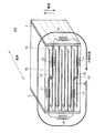
- FIG. 1 is a schematic external view of a capacitor-type resonator 300.
- FIG. It is the II-II sectional view taken on the line shown in FIG. It is a figure for demonstrating the resonant circuit formed with the capacitor
- 6 is a diagram illustrating an example of frequency characteristics of relative permeability generated in the capacitor-type resonator 300.
- FIG. 3 is a diagram showing a metamaterial having a negative dielectric constant using a coiled resonator 100.
- FIG. It is a figure which shows the relative magnetic permeability of the metamaterial shown in FIG. It is a figure which shows the dielectric constant of the metamaterial shown in FIG.
- FIG. 3 is a diagram illustrating a metamaterial having a negative magnetic permeability using a coiled resonator 100.
- FIG. It is a figure which shows the relative magnetic permeability of the metamaterial shown in FIG. It is a figure which shows the dielectric constant of the metamaterial shown in FIG. It is a figure which shows the capacitor
- FIG. 3 is a perspective view of a unit 600.
- FIG. 2 It is the side view which looked at the unit 600 from the y direction.
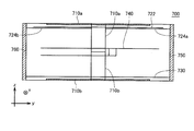
- 3 is a perspective view of a unit 700.
- FIG. 3 is a side view of a unit 700.
- FIG. 4 is a perspective view of a unit 800.
- FIG. 3 is a side view of a unit 800.
- FIG. 4 is a top view of a unit 800.
- FIG. 2 is a perspective view of a unit 900.
- FIG. 3 is a front view of a unit 900.
- FIG. 2 is a side view of a unit 900.
- FIG. It is a figure for demonstrating the production method of the unit 900 which concerns on 5th Embodiment. It is a figure which shows the structure of the unit 1000 which concerns on 6th Embodiment. It is the figure which showed typically the positional relationship of the metamaterial which combined the split ring type
- FIG. It is a figure which shows typically the mode of an electric charge and an electric field when the metamaterial shown in FIG. 32 shows a negative dielectric constant. It is a figure which shows typically the mode of a magnetic field when the metamaterial shown in FIG. 32 shows a negative magnetic permeability. It is the figure which showed typically the positional relationship of the metamaterial from which the arrangement
- FIG. It is a figure for demonstrating the area
- 35 shows a negative magnetic permeability. It is a figure which shows transmission of the electromagnetic wave on a transmission line for every range of the value of magnetic permeability (mu) and dielectric constant (epsilon). It is a figure which shows the antenna using the metamaterial which concerns on 7th Embodiment. It is a figure which shows in more detail the antenna using the metamaterial which concerns on 7th Embodiment. It is a figure which shows the example of the structure which forms the antenna using the metamaterial which concerns on 7th Embodiment. It is a figure which shows the structure of the simulation of the resonance of the electromagnetic wave in the metal flat plate when not using a metamaterial.
- FIG. 71 is a diagram showing an arrow AA in FIG. 70. It is a perspective view of the structure of the antenna using the slit which concerns on 26th Embodiment. It is a figure for demonstrating the case where multiple conventional slot antennas are provided in the same metal flat plate. It is a figure for demonstrating the case where multiple antennas using the slit which concerns on 27th Embodiment are provided in the same metal flat plate. It is a figure which shows arrangement
- metamaterials are an artificial material having electromagnetic or optical characteristics that a substance existing in nature does not have.
- Typical properties of such metamaterials include negative permeability ( ⁇ ⁇ 0), negative dielectric constant ( ⁇ ⁇ 0), or negative refractive index (when both permeability and dielectric constant are negative) Is mentioned.
- the region of ⁇ ⁇ 0 and ⁇ > 0, or the region of ⁇ > 0 and ⁇ ⁇ 0 is also referred to as “evanescent solution region”, and the region of ⁇ ⁇ 0 and ⁇ ⁇ 0 is also referred to as “left-handed region”.
- Left-handed metamaterials with ⁇ ⁇ 0 and ⁇ ⁇ 0 have a periodic arrangement of elements with negative permittivity and elements with negative permeability in order to simultaneously realize negative permittivity and negative permeability. Made.
- the left-handed metamaterial can be broadly divided into a circuit system and a resonance system.
- a split ring resonator for example, “left-handed metamaterial” (Nikkei Electronics January 2 issue, Nikkei BP) , January 2, 2006, pages 75-81)).
- the metamaterial cannot be miniaturized by a method using a thin metal wire sufficiently long with respect to the wavelength of the electromagnetic wave for realizing negative ⁇ . Therefore, it is conceivable to use a metal wire having a length half the wavelength ⁇ of the electromagnetic wave.
- the ⁇ / 2 long metal wire is a kind of resonator.
- the combination of the metal wire and the resonator may not exhibit negative ⁇ and negative ⁇ simultaneously.
- the left-handed metamaterial according to the present invention is a resonant system in which resonators are combined. Therefore, first, a resonator constituting the left-handed metamaterial of the present invention will be described.
- One of the resonators used in the present embodiment is a multilayer capacitor type resonator including a plurality of electrodes.
- a resonance circuit mainly composed of electrostatic capacitance (capacitance) generated between the electrodes is formed.
- This resonant circuit is sensitive to a specific frequency component of the electromagnetic wave generated by the alternating current flowing in the signal line arranged around the resonator, and generates an electrical resonance phenomenon by receiving the electromagnetic wave of this frequency component. obtain. Due to this resonance phenomenon, negative magnetic permeability appears.
- the length of each resonator in the propagation direction of the current is at least ⁇ with respect to the wavelength ⁇ of the electromagnetic wave at the frequency to be targeted. Must be shorter than / 4. Furthermore, the length of each resonator in the current propagation direction is preferably ⁇ / 20 or less.
- a multilayer capacitor formed by laminating a plurality of plate electrodes with an insulator (dielectric) can be used.
- achieves a resonator using a multilayer capacitor is illustrated.
- the resonator can be easily configured using a multilayer capacitor such as a commercially available multilayer ceramic capacitor.
- FIG. 1 is a schematic external view of a capacitor-type resonator 300.
- a capacitor resonator 300 is covered with an exterior part 10 that is a nonmagnetic material.
- a resin material such as Teflon (registered trademark) is suitable.
- the capacitor-type resonator 300 is disposed close to the signal line 200 through which a current including a predetermined frequency component flows, so that it receives a specific frequency component (resonance frequency) of an electromagnetic wave generated by the current and resonates.
- a ground 220 is disposed on the surface of the capacitor type resonator 300 opposite to the surface in contact with the signal line 200.
- the capacitor type resonator 300 In order for the capacitor type resonator 300 to exhibit a negative magnetic permeability, that is, to exhibit a negative magnetic permeability that is a function as a metamaterial, in the current propagation direction in the signal line 200 of the capacitor type resonator 300.
- the length l ′ needs to be at least shorter than ⁇ / 4 with respect to the wavelength ⁇ of the electromagnetic wave at the resonance frequency. Furthermore, the length l of the capacitor resonator 300 is preferably ⁇ / 20 or less.
- the distance h between the signal line 200 and the multilayer capacitor is 0.2 mm, and the distance between the multilayer capacitor and the ground h ′ is 0.2 mm.
- this capacitor type resonator 300 is arranged at a pitch of ⁇ / 4 or less, it can be used as a metamaterial in the gigahertz band.
- the length l of the resonator can be appropriately designed according to the frequency region to be applied.
- FIG. 2 is a cross-sectional view taken along line II-II shown in FIG.
- an alternating magnetic field is generated in the circumferential direction around signal line 200. That is, the magnetic field lines of the magnetic field are concentric circles with the signal line 200 as the center. Further, since an electric potential is generated when a current flows through the signal line 200, an alternating electric field is generated between the signal line 200 and the ground 220.
- the capacitor-type resonator 300 includes a plurality of first internal electrodes 4 and a plurality of second internal electrodes 5 that are opposed to each other with spacers 6 each being an insulator having a high relative dielectric constant.
- the plurality of first internal electrodes 4 are electrically connected to the first external electrode 2, and the plurality of second internal electrodes 5 are electrically connected to the second external electrode 3.
- the plurality of plate-like internal electrodes 4 and 5 are laminated, and the area of the electrode is between the adjacent first internal electrode 4 and second internal electrode 5. Then, a capacitance (capacitance) whose value is determined by the distance between the electrodes, the relative dielectric constant of the spacer 6 and the like is generated.
- the electrode surfaces of the first internal electrode 4 and the second internal electrode 5 constituting the capacitor resonator 300 are arranged so as to be substantially parallel to the magnetic field lines of the magnetic field.
- the electrode surfaces of the first external electrode 2 and the second external electrode 3 are substantially different from the magnetic field lines on the surfaces different from the electrode surfaces of the first external electrode 2 and the second external electrode 3. It arrange
- the electrode cross-section longitudinal direction of the first external electrode 2 and the second external electrode 3 is arranged so that the longitudinal direction of the electrode cross-section coincides with the vertical direction of the paper.
- a resonance circuit as shown in FIG. 3 is formed with respect to a predetermined frequency component. Magnetic susceptibility develops.
- FIG. 3 is a diagram for explaining a resonance circuit formed by the capacitor-type resonator 300 at the resonance frequency.
- the electrode 3 acts as a coil (inductor) according to the path length.
- the uppermost electrode 4a of the first internal electrodes, the first external electrode 2, and the lowermost electrode 4b of the first internal electrodes are electrically connected to each other. Is formed.
- the uppermost electrode 5a, the second outer electrode 3, and the lowermost electrode 5b of the second internal electrodes are electrically connected to each other, and a current path including these is connected. It is formed.
- both current paths are electrically connected to each other via the electrostatic capacitance (capacitance C1) between the electrode 4a and the electrode 5a and the electrostatic capacitance (capacitance C2) between the electrode 4b and the electrode 5b.
- a resonant circuit is formed which is connected and includes capacitances C1 and C2 and inductances L1 to L6 generated by the respective electrodes. Therefore, the capacitor-type resonator 300 according to the present embodiment has a resonance frequency determined by the capacitance (C1 + C2) and the inductance (L1 + L2 + L3 + L4 + L5 + L6), and permeability resonance occurs when an electromagnetic wave having this resonance frequency is incident.
- a capacitance is generated between the adjacent internal electrodes.
- the other capacitances except the uppermost capacitance and the lowest capacitance are the same.
- the influence on the formation of the resonant circuit is small. This is because current concentrates on the outermost layer of the circulation path causing resonance.
- FIG. 4 is a diagram illustrating an example of frequency characteristics of relative permeability generated in the capacitor-type resonator 300.
- the change characteristics shown in FIG. 4 are calculated by simulation.
- the relative magnetic permeability represents a ratio of magnetic permeability to vacuum magnetic permeability.
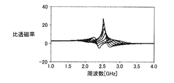
- the capacitor-type resonator 300 has about 4.9 GHz as one resonance frequency, and the relative permeability greatly fluctuates before and after the resonance frequency, resulting in a negative permeability.
- the electrode surfaces of the first internal electrode 4 and the second internal electrode 5, and the first external electrode 2 and the second external electrode 3 are arranged so as to be substantially parallel to the magnetic field lines of the magnetic field. It was described that negative permeability, which is a function as a metamaterial, can be expressed.
- substantially parallel means to exclude the state in which each electrode surface is orthogonal to the magnetic field lines of magnetic force, and in addition to the state in which each electrode surface is completely parallel to the magnetic field lines of magnetic field, Including a state having a predetermined angle. Practically, if the magnitude of the negative magnetic permeability developed in the capacitor-type resonator 300 is a value that can satisfy the requirements of the application, etc., it can be regarded as “substantially parallel”.
- the capacitor type resonator has a negative magnetic permeability
- the coil type resonator is arranged so that the central axis is parallel to the electric field direction (perpendicular to the magnetic field).
- a negative dielectric constant can be realized.
- the coiled resonator arranged so that the central axis is perpendicular to the electric field direction (parallel to the magnetic field direction) can achieve negative magnetic permeability.
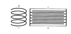
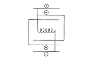
- FIG. 5 is a diagram for explaining a configuration of a metamaterial that develops a negative dielectric constant using a coil-type resonator.
- the metamaterial includes a coiled resonator 100 and an exterior part 10.
- the coiled resonator 100 is covered with an exterior part 10 that is a non-magnetic material.
- the coiled resonator 100 is disposed between the signal line 200 and the ground 220.
- the ground 220 is disposed on the surface of the exterior portion 10 on the surface opposite to the surface in contact with the signal line 200 of the coiled resonator 100.
- the signal line 200 is a strip line.
- the signal line 200 is an example of a conductor through which a current flows, and the form of the conductor is not limited to this.
- the coil-type resonator 100 is a metal wire.
- the total length of the coiled resonator 100 (the total length of the metal wire) is about half of the wavelength of the current flowing through the signal line 200.
- the frequency of the current flowing through the signal line 200 is in the GHz band, and the length of the coiled resonator 100 is 28 mm.
- FIG. 5 shows the coil-type resonator 100 wound around the central axis 110, that is, having a spring shape.
- the shape of the coil-type resonator 100 is not limited to that shown in FIG.
- the coiled resonator 100 may have a shape that is wound along a quadrangular prism.
- the coiled resonator 100 may have a shape wound along a spherical surface.
- the coiled resonator 100 only needs to have the length and shape as described above.
- a coil type resonator 100 a coil wound with a metal wire or the like can be used.
- a pre-made one for example, a pre-made coil
- a dedicated one may be used.
- the exterior part 10 fixes the position of the coiled resonator 100.
- a resin material such as Teflon (registered trademark) is suitable.
- Teflon registered trademark
- the exterior part 10 is an example of a support member that fixes the position of the coiled resonator 100, and the coiled resonator 100 may be fixed by another member.
- the central axis 110 of the coiled resonator 100 is parallel to the electric field generated by the current flowing through the signal line 200, more specifically, the electric field generated between the signal line 200 and the ground 220. That is, the exterior part 10 fixes the coiled resonator 100 so that the central axis 110 is parallel to the electric field. In other words, the coiled resonator 100 is arranged so that there is a difference in potential between both ends of the coil along the gradient of the electric field.
- the central axis 110 is in the direction from the signal line 200 toward the ground 220. That is, the central axis 110 is orthogonal to the ground 220 plane and penetrates the signal line 200. With this arrangement, the central axis 110 is parallel to the electric field generated by the current flowing through the signal line 200 (perpendicular to the magnetic field generated by the current flowing through the signal line 200).
- the coiled resonator 100 receives a specific frequency (resonance frequency) component of the electric field generated by the current flowing through the signal line 200, thereby causing resonance.
- the electromagnetic properties of the coiled resonator 100 are shown in FIGS.
- the relative permeability and relative permittivity of the metamaterial shown in FIG. 5 are shown in FIGS. 6 and 7, respectively.
- the relative dielectric constant represents the ratio of the dielectric constant to the vacuum dielectric constant
- the relative magnetic permeability represents the ratio of the magnetic permeability to the vacuum magnetic permeability.
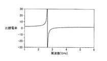
- the metamaterial of FIG. 5 exhibits a negative dielectric constant near 2.6 GHz.
- the relative magnetic permeability is always positive as shown in FIG.
- a negative dielectric constant is expressed by a coiled metal wire having a length of 1 ⁇ 2 of the wavelength.
- a metamaterial using a coiled metal wire can be made smaller than a metamaterial that achieves a negative dielectric constant using a straight metal wire.
- the metamaterial having negative ⁇ is realized by placing the coil type resonator 100 having the same length and shape as the coil type resonator 100 shown in FIG. 5 so that the central axis 110 is parallel to the magnetic field. Is done.
- the fact that the coiled resonator 100 arranged in this manner exhibits a negative magnetic permeability will be described below with reference to FIGS.
- FIG. 8 is a diagram for explaining the configuration of a metamaterial that develops a negative dielectric constant using a coil-type resonator.
- the metamaterial shown in FIG. 8 rotates the coiled resonator 100 shown in FIG. 6 90 degrees around the Y axis, and the central axis of the coiled resonator 100 is parallel to the magnetic field generated by the current flowing through the signal line 200 ( It is arranged so as to be perpendicular to the electric field generated by the current flowing through the signal line 200.
- FIG. 9 and FIG. 10 show the relative permeability and relative permittivity of the metamaterial shown in FIG. As shown in FIG. 9, the metamaterial of FIG. 8 exhibits a negative permeability near 2.6 GHz. On the other hand, as shown in FIG. 10, the relative dielectric constant is always positive.
- the coiled resonator 100 having the same structure may exhibit a negative dielectric constant or a negative magnetic permeability.
- each resonator In order for the combination of these resonators to become a left-handed metamaterial, that is, to simultaneously exhibit a negative magnetic permeability and a negative dielectric constant, the arrangement and structure of each resonator are important. First, each resonator must be arranged so that the coil-type resonator exhibits a negative dielectric constant and the capacitor-type resonator exhibits a negative magnetic permeability. Furthermore, it is necessary to consider the structure of the resonator so that the resonators do not cause inappropriate interference.
- the coil type resonator may be arranged so that its axis is parallel to the electric field direction (the z direction).
- the inner pole plate is parallel to the magnetic field direction, that is, a plane (xy plane) normal to the z-direction so that the capacitor-type resonator exhibits negative permeability. ) So as to be parallel to each other.
- the capacitor-type resonator preferably satisfies the condition that the outermost two internal electrodes are in reverse phase, that is, the signs of charges stored in the respective internal electrodes are opposite. This is to avoid interference between the capacitor-type resonator and the coil-type resonator.
- this will be described in more detail with reference to FIGS.
- FIG. 11 is a diagram showing a capacitor-type resonator and a coil-type resonator to which the outermost internal electrodes are directly connected. These resonators are arranged close to each other. However, the coil type resonator and the capacitor type resonator are not in electrical contact with each other. Since the coiled resonator is placed in an electric field, different signs of charge appear at both ends.
- FIG. 11 shows a situation where a positive charge (+ in FIG. 11) appears at the upper end and a negative charge ( ⁇ in FIG. 11) appears at the lower end. At the anti-resonance frequency, the sign of the charge at both ends is reversed, an electric field vector in the opposite direction is generated, and a negative dielectric constant is expressed.
- FIG. 11 of the capacitor-type resonator are electrically connected directly by the uppermost electrode by the external electrode, and therefore, charge of the same sign is stored.
- FIG. 11 shows a case where the uppermost electrode and the lowermost electrode are negatively charged.
- FIG. 12 is a diagram showing the relative dielectric constant of the resonator group shown in FIG.
- FIG. 13 is a diagram showing the relative permeability of the resonator group shown in FIG.
- FIG. 12 shows the relative dielectric constant characteristics of the entire resonator group when the shape (length, etc.) of the coiled resonator is changed. According to the shape change of the coil type resonator, the resonance frequency of the dielectric constant changes, and thus the frequency at which the negative dielectric constant is generated changes.
- FIG. 13 shows the relative permeability characteristics of the entire resonator group when the shape (length, etc.) of the coiled resonator is changed.
- the resonance frequency of the magnetic permeability changes, and therefore the frequency at which the negative magnetic permeability is generated changes.
- the change in the resonance frequency of the magnetic permeability despite the fact that the shape of the capacitor type resonator is not changed is due to the interference of the charges at the end of each resonator.
- both the band where the negative dielectric constant is generated and the band where the negative permeability is generated change. Therefore, the negative dielectric constant and the negative magnetic permeability cannot be expressed at the same frequency.
- the frequency indicating the negative dielectric constant (permeability) is increased, the frequency indicating the negative magnetic permeability (dielectric constant) also increases. Conversely, if the frequency indicating the negative dielectric constant (permeability) is decreased, the frequency indicating the negative magnetic permeability (dielectric constant) is also decreased.
- the metamaterial according to the present embodiment includes a coil-type resonator 100, a capacitor-type resonator 300, and an exterior part 10 (not shown in FIG. 14).
- the exterior portion 10 fixes the capacitor-type resonator and the coil-type resonator at positions close to each other. Similar to the above description, other support members may be used instead of the exterior portion 10.
- FIG. 14 shows a situation in which a positive charge (+ in FIG. 14) appears at the upper end and a negative charge ( ⁇ in FIG. 14) appears at the lower end, as in FIG.
- a positive charge (+ in FIG. 14) appears at the upper end
- a negative charge ⁇ in FIG. 14
- the sign of the charge at both ends is reversed, an electric field vector in the opposite direction is generated, and a negative dielectric constant is expressed.
- the capacitor type resonator is different from that shown in FIG.
- the uppermost electrode and the lowermost electrode in FIG. 14 of the capacitor-type resonator are not electrically directly connected by an external electrode, but are connected via an electric capacity. Therefore, the uppermost electrode and the lowermost electrode are in opposite phases (stores charges with opposite signs).
- FIG. 14 shows a case where the uppermost electrode has a negative charge and the lowermost electrode has a positive charge.
- FIG. 15 shows the relative dielectric constant characteristics of the entire resonator group when the shape of the coiled resonator is changed. According to the shape change of the coil type resonator, the resonance frequency of the dielectric constant changes, and thus the frequency at which the negative dielectric constant is generated changes.
- FIG. 16 shows the relative permeability characteristics of the entire resonator group when the shape of the coil-type resonator is changed. Even if the shape of the coil-type resonator is changed, the resonance frequency of the magnetic permeability does not substantially change. This is because charge interference at the end of each resonator is suppressed, and the resonance characteristics of the capacitor-type resonator do not change.
- the metamaterial according to the present embodiment can generate a negative dielectric constant and a negative magnetic permeability at the same time, and becomes a left-handed system.
- the metamaterial may include a plurality of sets.
- the set is fixed by a support member at a one-dimensional or two-dimensional continuous position.
- the resonator having a negative ⁇ is not limited to a coil-type resonator, and a resonator including a line having a length of approximately ⁇ / 2 that resonates with an electromagnetic wave can be used.
- the resonator having negative ⁇ and the resonator having negative ⁇ are not necessarily arranged side by side. Absent.
- a resonator having negative ⁇ a resonator including a ⁇ / 2 length line and two conductive plates connected to both ends of the line is used, and a resonator having negative ⁇ . And a configuration in which a capacitor-type resonator having a negative ⁇ is combined in a common space.
- FIG. 18 is a schematic diagram of a metamaterial according to the second embodiment.
- FIG. 17 shows the metamaterial of the second embodiment in which the configuration of the capacitor type resonator is changed.
- two conductive plates are arranged outside the two outermost electrodes of the capacitor resonator so as to face the outermost electrodes.
- the conductive plates are connected by a wound line.
- the line is designed so that its length is approximately ⁇ / 2 of the resonance wavelength.
- the track Since the track is wound, its length can be secured in a small space.
- the line may not be wound depending on the resonance wavelength or when downsizing is not necessary.
- 17 and 18 show the line wound in a coil shape, but downsizing is not limited to the method of winding the line, and can be realized by bending the line. For example, a meander line may be used.
- each conductive plate increases the capacitance between the line and the absolute value of the negative dielectric constant at the resonance frequency.
- the substantial length of ⁇ / 2 can be shortened by the wavelength shortening effect due to the capacitance.
- each conductive plate may not be installed. Further, the conductive plate may be connected to only one end of the line for design reasons.
- FIG. 17 The difference between FIG. 17 and FIG. 18 is that in FIG. 17, the two outermost electrodes of the capacitor-type resonator are directly connected, whereas in FIG. In that point. Since the metamaterial according to the present embodiment shown in FIG. 18 can suppress the interference of electric charges similarly to the metamaterial according to the first embodiment, the negative permittivity and the negative permeability can be expressed simultaneously. Can do. In the structure shown in FIG. 17, it is difficult to simultaneously develop a negative dielectric constant and a negative magnetic permeability.
- FIG. 19 shows a specific configuration of the metamaterial according to the present embodiment schematically shown in FIG.
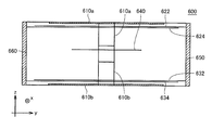
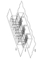
- the metamaterial according to the present embodiment includes a plurality of units 600 in which a negative dielectric constant resonator and a negative magnetic permeability resonator are formed in a substrate material.
- a negative dielectric constant resonator and a negative magnetic permeability resonator are formed in one chip by using a technique such as a multilayer substrate.
- the substrate material corresponds to the support member.
- Each unit 600 is disposed immediately below the signal line 200 and between the signal line 200 and the ground 220. Each unit 600 is arranged spatially continuously.
- FIG. 19 shows an example in which four units 600 are arranged in a direction along the signal line 200, the arrangement of the units 600 is not limited to this. It is also possible to arrange the one-dimensionally arranged resonators in the same plane to form a planar metamaterial. Furthermore, a planar metamaterial can be stacked to form a three-dimensional metamaterial.
- FIG. 20 is a perspective view of the unit 600.
- FIG. 21 is a side view of the unit 600 as viewed from the y direction.
- the unit 600 includes an uppermost electrode 610a, a lowermost electrode 610b, a first internal electrode 622, a second internal electrode 624, a third internal electrode 632, and a fourth An internal electrode 634 and a line 640 are provided. As shown in FIG. 21, the unit 600 further includes a first external electrode 650 and a second external electrode 660.
- the uppermost electrode 610a is disposed above the first internal electrode 622, the second internal electrode 624, the third internal electrode 632, and the fourth internal electrode 634 (at a position where the z coordinate is large).
- the lowermost electrode 610b is disposed below the first internal electrode 622, the second internal electrode 624, the third internal electrode 632, and the fourth internal electrode 634 (where the z coordinate is small).
- the uppermost electrode 610a has a side surface portion extending in the ⁇ z direction.
- the lowermost electrode 610b has a side surface portion extending in the + z direction. Further, the uppermost electrode 610 a is disposed directly below the signal line 200.
- the line 640 connects the side surface portion of the uppermost electrode 610a extending in the ⁇ z direction and the side surface portion of the lowermost electrode 610b extending in the + z direction.
- the line 640 functions as a part of a ⁇ / 2 line that realizes a negative dielectric constant by connecting the uppermost electrode 610a and the lowermost electrode 610b to each side surface portion.
- the length of the line composed of the line 640 and each side part is designed according to the resonance frequency.
- the line 640 is a meander line drawn in the center layer.
- the shape of the line 640 is not limited to this, and may be helical or spiral, for example.
- the uppermost electrode 610a and the lowermost electrode 610b are provided for increasing the absolute value of the negative dielectric constant and shortening the resonance wavelength.
- the resonance wavelength is shortened by the wavelength shortening effect due to the capacitance between the uppermost electrode 610a and the signal line.
- the uppermost electrode 610a and the lowermost electrode 610b can be omitted depending on the required negative dielectric constant and resonance wavelength.
- the first internal electrode 622 and the second internal electrode 624 are disposed in close proximity to each other.
- the third internal electrode 632 and the fourth internal electrode 634 are disposed close to and opposed to each other.
- a pair of first internal electrode 622 and second internal electrode 624 (referred to as an upper electrode pair) is disposed on the uppermost electrode 610a side.
- a pair of the third internal electrode 632 and the fourth internal electrode 634 (referred to as a lower electrode pair) is disposed on the lowermost electrode 610b side.
- Each internal electrode surface is disposed in parallel to the direction of the magnetic field generated by the current flowing through the signal line 200 (perpendicular to the electric field direction).
- the first external electrode 650 connects the first internal electrode 622 and the third internal electrode 632 as shown in FIG. As shown in FIG. 21, the second external electrode 660 connects the second internal electrode 624 and the fourth internal electrode 634.
- Each external electrode surface is disposed parallel to the direction of the magnetic field generated by the current flowing through the signal line 200 (perpendicular to the electric field direction).
- the line 640, the uppermost electrode 610a, and the lowermost electrode 610b described above realize a negative dielectric constant.
- the first to fourth internal electrodes 622, 624, 632, 634, the first external electrode 650, and the second external electrode 660 form a capacitor-type resonator having two upper and lower electrodes, and are negative. Realize permeability.
- the ⁇ / 2 line that realizes the negative dielectric constant and the capacitor-type resonator that realizes the negative magnetic permeability are not directly electrically connected to each other.
- the ⁇ / 2 line and the capacitor type resonator are not electrically connected to the signal line 200 and the ground 220, and are in a floating state. Further, the units 600 are not in contact with each other.
- the metamaterial according to the present embodiment functions as a left-handed metamaterial.
- the arrangement of the units 600 is not limited to the above. For example, it may be arranged two-dimensionally in a plane.
- the metamaterial according to the present embodiment is created by forming a negative dielectric resonator and a negative magnetic permeability resonator in the unit, industrial production is easy.
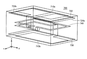
- FIG. 22 and FIG. 23 show the structure of one unit 700 of the metamaterial according to the third embodiment.
- FIG. 22 is a perspective view of the unit 700.
- FIG. 23 is a side view of the unit 700.
- unit 700 includes an uppermost electrode 710a, a lowermost electrode 710b, a first internal electrode 722, a second internal electrode 724a, a third internal electrode 724b, and a fourth An internal electrode 730 and a line 740 are provided.
- unit 700 further includes a first external electrode 750 and a second external electrode 760.
- the uppermost electrode 710a and the lowermost electrode 710b have the same structure as the uppermost electrode 610a and the lowermost electrode 610b according to the second embodiment, and are arranged outside the internal electrodes.
- the line 740 connects the uppermost electrode 710a and the lowermost electrode 710b.
- the line 740 functions as a part of the ⁇ / 2 line and realizes a negative dielectric constant, like the line 640 of the second embodiment.
- the line 740 has a helical structure that makes a half turn in the horizontal plane.
- the second internal electrode 724a and the third internal electrode 724b are arranged apart from each other in the same plane.
- the first external electrode 750 connects the second internal electrode 724 a and the fourth internal electrode 730.
- the second external electrode 760 connects the third internal electrode 724 b and the fourth internal electrode 730. That is, the second internal electrode 724a, the first external electrode 750, the third internal electrode 724b, the second external electrode 760, and the fourth internal electrode 730 have a structure similar to that of the split ring resonator. . Therefore, these electrodes develop a negative magnetic permeability.
- the first internal electrode 722 is arranged to face the second internal electrode 724a and the third internal electrode 724b so as not to be in electrical contact with the second internal electrode 724a and the third internal electrode 724b.
- the The first internal electrode 722 supplements the capacitance at the break between the second internal electrode 724a and the third internal electrode 724b, and serves to lower the resonance frequency.
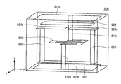
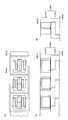
- FIG. 24 is a perspective view of the unit 800.
- FIG. 25 is a side view of the unit 800.
- FIG. 26 is a top view of the unit 800.
- the unit 800 includes a coiled conductor 810, a first electrode 822, a second electrode 824, a third electrode 832, a fourth electrode 834, a first via 842, and a second via 844.
- the coiled conductor 810 circulates in a plurality of regions (eight times in the example shown here) close to the surface of the unit 800.
- the coiled conductor 810 is disposed so as to surround the first electrode 822, the second electrode 824, the third electrode 832, the fourth electrode 834, the first via 842, and the second via 844.
- the first electrode 822 and the second electrode 824 are disposed in close proximity to each other. Further, the first electrode 822 and the second electrode 824 are arranged with their positions in the horizontal plane being shifted from each other.
- the third electrode 832 and the fourth electrode 834 are disposed close to and opposed to each other. In addition, the third electrode 832 and the fourth electrode 834 are arranged with their positions in the horizontal plane shifted from each other.
- the pair of the first electrode 822 and the second electrode 824 is formed in the upper part in the unit 800.
- the pair of the third electrode 832 and the fourth electrode 834 is formed in the lower part in the unit 800.
- the upper part and the lower part here are based on FIG. 24 and FIG.
- the first via 842 connects the first electrode 822 and the third electrode 832.
- the second via 844 connects the second electrode 824 and the fourth electrode 834.
- the first to fourth electrodes 822, 824, 832, 834, the first via 842, and the second via 844 function as a capacitor-type resonator and develop negative magnetic permeability.
- the length of the line (coil) can be increased while maintaining the size of the unit as compared with the second and third embodiments. Therefore, a low resonance frequency can be obtained.
- the negative magnetic permeability resonator is an external electrode for connecting the internal electrode.
- the conductive portion for connecting the internal electrode is realized by a via.
- FIG. 27 to FIG. 29 show the structure of one metamaterial unit 900 according to the fifth embodiment.
- FIG. 27 is a perspective view of the unit 900.
- FIG. 28 is a front view of the unit 900.
- FIG. 29 is a side view of the unit 900.
- the unit 900 includes an uppermost electrode 910a, a first via 912a, a second via 912b, a lowermost electrode 910b, a first internal electrode 922, and a second
- the internal electrode 924a, the third internal electrode 924b, the fourth internal electrode 930, the line 940, the third via 950, and the fourth via 960 are provided.
- the first via 912a, the line 940, and the second via 912b connect the uppermost electrode 910a and the lowermost electrode 910b.
- the total length of the first via 912a, the line 940, and the second via 912b is approximately half the resonance wavelength.
- the first via 912a, the line 940, and the second via 912b function as part of the ⁇ / 2 line and realize a negative dielectric constant.
- the shape of the line 940 is not limited to the meander line shown in the figure, and may be helical or spiral, for example.
- the uppermost electrode 910a and the lowermost electrode 910b exhibit the functions of increasing the absolute value of the negative dielectric constant and shortening the resonance wavelength, like the uppermost electrode 610a and the lowermost electrode 610b shown in FIG. However, the uppermost electrode 910a and the lowermost electrode 910b can be omitted.
- the outer end of the first via 912a (the end not connected to the line 940) and the outer end of the second via 912b (the end not connected to the line 940) are Regardless of the presence or absence of the upper electrode 910a and the lowermost electrode 910b, it is preferable to be outside the negative permeability resonator so that electric charges are accumulated at both ends of the ⁇ / 2 line.
- the third via 950 connects the second internal electrode 924a and the fourth internal electrode 930.
- the fourth via 960 connects the third internal electrode 924 b and the fourth internal electrode 930.
- the second internal electrode 924a, the third via 950, the third internal electrode 924b, the fourth via 960, and the fourth internal electrode 930 have a structure similar to that of the split ring type resonator, and are negative. It functions as a resonator that exhibits magnetic permeability.
- the first internal electrode 922 compensates for the capacitance of the cut portion between the second internal electrode 924a and the third internal electrode 924b, similarly to the first internal electrode 722 of the fourth embodiment. It plays a role of lowering the resonance frequency.
- the unit 900 according to this embodiment does not require an external electrode. This unit is therefore easy to manufacture.
- a unit including an external electrode is created, usually, after a portion other than the external electrode is laminated, the external electrode is attached to the laminated part.
- the unit 900 according to the present embodiment can be created only by stacking.
- the unit 900 is suitable for creating a metamaterial in which a plurality of units are arranged.
- unit processing such as arranging the units apart from each other or covering the external electrode with an insulator. Since the units 900 according to the present embodiment can be arranged adjacent to each other, the metamaterial can be further reduced. Further, since no processing is required, creation of a metamaterial using the unit 900 is easy.
- FIG. 30 is a diagram for explaining a method of creating the unit 900 according to the sixth embodiment.
- the unit 900 is created by sequentially stacking a plurality of layers.
- FIG. 30 shows layers L 1 to L 6 including the main components of the unit 900.
- the material (substrate material) of each layer is an insulating material such as a resin.
- Metal parts are formed on several layers of substrate material. Further, vias are formed in some layers of the substrate material so as to penetrate the substrate material.
- FIG. 30 shows a part of the layers L1 to L6. Actually, the layers L1 to L6 further extend in the lateral direction in FIG.
- the layer L1 includes a plurality of bottom electrodes 910b.
- the layer L2 includes a plurality of fourth internal electrodes 930.
- the layer L3 includes a plurality of lines 940.
- the layer L4 includes a plurality of pairs of the second internal electrode 924a and the third internal electrode 924b.
- the layer L5 includes a plurality of first internal electrodes 922.
- Layer L6 includes a plurality of top electrodes 910a.
- vias are formed in regions corresponding to the first via 912a, the second via 912b, the third via 950, and the fourth via 960.
- vias are indicated by thin vertical lines.
- the laminate After stacking each layer to make a laminate, the laminate is cut to create a unit 900.
- Nine units 900 are formed from the portion shown in FIG.
- several units 900 may be cut out from the laminated body as a group.
- the structure in which the conductive portion of the split resonator shown in the third embodiment is a via is shown, but the conductive portion of another type of resonator can be a via.
- the external electrode of the multilayer capacitor type resonator shown in the second embodiment may be a via.
- a line for expressing a negative dielectric constant is connected to an LC resonator (specifically, a multilayer capacitor type resonator and a split type resonator).
- the line does not necessarily have to be inside the LC resonator.
- a unit 1000 in which a ⁇ / 2 line is disposed outside the LC resonator will be described.
- FIG. 31 shows the structure of a unit 1000 according to the sixth embodiment.
- FIG. 31 is a diagram showing a structure of a unit 1000 according to the sixth embodiment.
- unit 1000 includes an uppermost electrode 1010a, a first via 1012, a lowermost electrode 1010b, a first internal electrode 1022, a second internal electrode 1024a, and a third internal electrode.
- An electrode 1024b, a fourth internal electrode 1030, a second via 1050, and a third via 1060 are provided.
- the first via 1012 connects the uppermost electrode 1010a and the lowermost electrode 1010b.
- the length of the first via 1012 is approximately 1 ⁇ 2 of the resonance wavelength. Therefore, the first via 1012 exhibits a negative dielectric constant with respect to the electromagnetic wave having the resonance wavelength.
- the uppermost electrode 1010a and the lowermost electrode 1010b are connected by a straight first via 1012.
- a ⁇ / 2 line may be realized by combining a plurality of vias and a line in a horizontal plane as in the structure shown in FIG.
- the line in this case is preferably a bent one such as a meander line as described in other embodiments.
- the top electrode 1010a and the bottom electrode 1010b like the top electrode 910a and the bottom electrode 910b in the fifth embodiment, increase the absolute value of the negative dielectric constant and reduce the resonance frequency. To do.
- the second internal electrode 1024a, the second via 1050, the third internal electrode 1024b, the fourth internal electrode 1030, the third via 1060, and the third internal electrode 1024b are split ring type resonators. It has the same structure and functions as a resonator that develops negative magnetic permeability. Similar to the first internal electrode 722 of the fourth embodiment, the first internal electrode 1022 compensates for the capacitance of the cut portion between the second internal electrode 1024a and the third internal electrode 1024b, It plays a role of lowering the resonance frequency.
- the first internal electrode 1022, the second internal electrode 1024a, the second via 1050, the third internal electrode 1024b, the third via 1060, and the fourth internal electrode 1030 are the uppermost electrode 1010a and the lowermost electrode. It arrange
- the unit 1000 according to the present embodiment can be easily created because the internal electrodes are connected by vias, similarly to the unit 900 according to the fifth embodiment. Moreover, since the unit 1000 does not have an electrode on the surface of the unit, it is suitable for creating a metamaterial.
- FIG. 32 is a diagram schematically showing a positional relationship between a metamaterial that is a combination of the split ring resonator 1210 and the half-wave resonator 1220, the signal line 200, and the ground 220.
- this metamaterial simultaneously exhibits a negative magnetic permeability and a negative dielectric constant. This is because the region where the electric field concentrates when the metamaterial resonates with the electromagnetic field does not overlap the region where the magnetic field concentrates.
- FIG. 33 is a diagram schematically showing the state of electric charge and electric field when the metamaterial shown in FIG. 32 shows a negative dielectric constant.
- half-wave resonator 1220 includes a first outermost electrode 1222, a second outermost electrode 1224, and a line 1226.
- the first outermost electrode 1222 is disposed on the signal line 200 side.
- the second outermost electrode 1244 is disposed on the ground 220 side.
- FIG. 33 shows a situation where a current flows through the signal line 200 and an electric field is generated from the signal line 200 toward the ground 220.
- a current having a resonance frequency flows, negative charge is accumulated in the first outermost electrode 1222 and positive charge is accumulated in the second outermost electrode 1224.
- a large electric field is generated in a region 1230 between the first outermost electrode 1222 and the signal line 200 and a region 1240 between the second outermost electrode 1224 and the ground 220.
- the region sandwiched between the end of the half-wave resonator 1220 where charges are accumulated by half-wave resonance and the signal line 200 or the ground is a region where the electric field due to resonance is concentrated.
- the electrodes connected to both ends of the half-wavelength line correspond to the ends of the half-wave resonator 1220.
- both ends of the half-wave line correspond to end portions of the half-wave resonator 1220.
- split ring resonator 1210 includes a first conductor 1212 and a second conductor 1214.
- FIG. 34 shows a situation in which a current flows through the signal line 200 and a magnetic field is generated from the split ring resonator 1210.
- a current having a resonance frequency flows, the current and the split ring resonator 1210 LC resonate, and a large magnetic field cancels out the magnetic field generated by the current flowing through the signal line 200 in the region 1250 inside the second conductor 1214.
- the generated magnetic field is mainly orthogonal to the paper surface.
- the internal region of the loop where the LC resonance occurs is a region where the magnetic field due to the resonance is concentrated.
- the space surrounded by the electrode pair that forms the capacitance and the conductive portion that forms the inductance is the region where the magnetic field due to resonance is concentrated.
- the region where the electric field concentrates region 1230 and region 1240
- the region where the magnetic field concentrates region 1250
- the metamaterial shown in FIG. 32 can simultaneously exhibit a negative dielectric constant and a negative magnetic permeability.
- the magnetic field generated by the magnetic permeability resonance is concentrated in a region different from the region where the electric field generated by the dielectric resonance is concentrated.
- FIG. 35 is a diagram schematically showing a positional relationship between a metamaterial having a different resonator arrangement from the metamaterial of FIG. 34, the signal line 200, and the ground 220.
- split ring resonator 1310 includes a split ring resonator 1310 and a half-wave resonator 1320.
- the metamaterial shown in FIG. Split ring resonator 1310 includes a first conductor 1312 and a second conductor 1314.
- the half-wave resonator 1320 is entirely disposed in the second conductor 1314.
- FIG. 36 is a diagram for explaining a region where an electric field concentrates when the metamaterial shown in FIG. 35 exhibits a negative dielectric constant.
- half-wave resonator 1320 includes a first outermost electrode 1322, a second outermost electrode 1324, and a line 1326.
- the first outermost electrode 1322 is disposed on the signal line 200 side.
- the second outermost electrode 1344 is disposed on the ground 220 side.
- FIG. 37 is a diagram for explaining a region where a magnetic field concentrates when the metamaterial shown in FIG. 35 exhibits negative magnetic permeability.
- a large magnetic field is generated in the region 1350 inside the second conductor 1314 in a direction that cancels the magnetic field generated by the current flowing through the signal line 200.
- metamaterials having other types of resonators also applies to metamaterials having other types of resonators.
- the above description also applies to a metamaterial in which a split resonator is replaced with a multilayer capacitor resonator.
- the resonator is configured so that charges of the same polarity are generated so far as not to affect each other's expression.
- the polarity of the outermost two outermost electrodes among the plurality of electrodes forming the electrostatic capacitance is opposite.
- FIG. 38 is a diagram showing transmission of electromagnetic waves on the transmission line for each range of values of magnetic permeability ⁇ and dielectric constant ⁇ . Referring to FIG. 38, electromagnetic waves are transmitted without being attenuated in the region of ⁇ > 1 and ⁇ > 1 and the region of ⁇ ⁇ 0 and ⁇ ⁇ 0 (the left-handed region described above).
- the MLCC multi-layer ceramic capacitor, multilayer ceramic capacitor
- the helical coil which can express the negative dielectric constant demonstrated in 1st Embodiment may be used, a chip coil may be used, and metal wire resin may be used.
- an LC resonator, a half-wave resonator, and a left-handed metamaterial chip may be used.
- the half-wave resonator may be a metal wire having a length of ⁇ / 2 which is not particularly molded.
- a resonator having a length of ⁇ / 4 may be used as long as a ground is provided on the opposite side across the metamaterial in the region 2000 of the metal casing 2001.
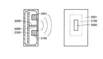
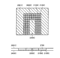
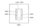
- FIG. 39 is a diagram illustrating an antenna using the metamaterial 2100 according to the seventh embodiment.
- a plurality of metamaterials 2100 as described above are attached to the inside of metal casing 2001 in a region that divides region 2000 desired to function as an antenna from other regions.
- the region of the metal housing 2001 to which the metamaterial 2100 is attached largely blocks the electromagnetic wave component equivalent to the high impedance region with respect to the electromagnetic wave component in the vicinity of the resonance wavelength of the metamaterial 2100.
- it is a region where the electromagnetic wave component is substantially blocked.
- the region 2000 is separated from other regions in resonance with the resonance wavelength component of the electromagnetic field.
- the region 2000 when power is supplied to the region 2000 from the circuit board 2300 via the feeder line 2200, the region 2000 is electromagnetically separated from other regions, and electromagnetic waves having components in the vicinity of the resonance wavelength of the metamaterial 2100 of the electromagnetic field are separated. It functions as an antenna that resonates with.
- part of the metal casing 2001 can function as an antenna. That is, even if the entire surface of the metal casing 2001 is metal, there is no need to provide an antenna outside, open a part of the casing, or use an insulator. For this reason, the cost can be reduced, the design can be given a degree of freedom, and the strength can be prevented from being lowered.
- a circuit for supplying power to the feeding point of the region 2000 functioning as an antenna through the feeder line 2200, and a circuit for processing an electromagnetic wave in the vicinity of the resonance wavelength resonated in the region 2000 functioning as the antenna. For example, a tuning circuit, an amplifier circuit, and an output circuit are mounted.
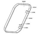
- the antenna is not limited to the rectangular antenna having a long side length of ⁇ / 4 and a short side length of less than ⁇ / 4 as shown in FIG.
- the antenna may be a strip-shaped antenna having a length of ⁇ / 4, may be folded into a meander shape to save space, may be an inverted F shape, or may be a folded dipole shape. There may be other shapes.
- the band of EBG Electromagnetic Band Gap
- the band of the antenna constituted by the region 2000 is widened. be able to.
- a resonance-type metamaterial when used as in this embodiment, a specific region 2000 can be electromagnetically separated by attaching the metamaterial to the back surface while keeping the surface of the metal housing as it is. . For this reason, there are advantages in terms of strength and design of the metal casing.
- the metal casing of an electric device such as a top panel of a notebook PC can be made to function as an antenna with all the metal, so the area usable as an antenna is wide. I can take it. For this reason, a plurality of antennas can be mounted. Even if a plurality of antennas are provided in the same metal casing, each antenna portion is separated by EBG, so that they are not electromagnetically coupled.
- the antenna of this embodiment is advantageous in terms of gain and bandwidth.
- the antenna using the metamaterial EBG is more disadvantageous than the metal antenna of the same size in terms of bandwidth and gain.
- such disadvantages can be compensated for by the advantage that the area of the antenna is not limited.
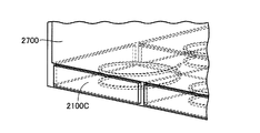
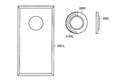
- FIG. 40 is a diagram showing in more detail an antenna using the metamaterial 2100 according to the seventh embodiment.
- a ground 2400 may be provided on the opposite side of region 2000 of metal casing 2001 with the metamaterial interposed therebetween. Further, the periphery of the ground 2400 may be connected to the metal casing 2001. As a result, the portion that functions as a shield remains, and the radiation surface of the antenna is mainly outside the metal housing 2001, so that the problem of noise can be eliminated.
- FIG. 41 is a diagram illustrating an example of a structure for forming an antenna using the metamaterial 2100 according to the seventh embodiment. Referring to FIG. 41, a chip coil is used as metamaterial 2100 in the present embodiment.
- the chip coil metamaterial 2100 is arranged and pasted, and a region 2000 is formed in the metal casing 2001 inside the region where the metamaterial 2100 is pasted. For this reason, even if the device is covered with the metal casing 2001, an antenna function can be added.
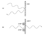
- FIG. 42 is a diagram showing a simulation structure of electromagnetic wave resonance in the metal flat plate 4001A when no metamaterial is used. 42, power supply line 4200A is connected to the back surface of the central portion of metal flat plate 4001A. In addition, ground flat plate 4400A is arranged at a minute distance from the back surface of metal flat plate 4001A.
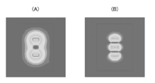
- FIG. 43 is a diagram showing a result of simulation of electromagnetic wave resonance in the metal flat plate 4001A when no metamaterial is used.
- FIG. 43 when power is supplied from the power supply line 4200A described with reference to FIG. 42, it resonates with electromagnetic waves of various frequencies of the electromagnetic field, whereby FIGS. 43 (A), 43 (B), and 43 (C).
- FIGS. 43 (A), 43 (B), and 43 (C) As shown in the figure, the simulation result of the electric field strength distribution showing various resonances is obtained with the whole metal flat plate 4001A.
- FIG. 44 is a diagram showing a simulation structure of electromagnetic wave resonance on a metal flat plate when a metamaterial is used.
- feed line 2200A is connected to the back surface of the central portion of metal flat plate 2001A.
- the ground flat plate 2400A is arranged at a minute distance from the back surface of the metal flat plate 2001A.
- the metamaterial 2100A is attached to an area that partitions the area including the feeding point to which the feeding line 2200A of the metal flat plate 2001A is connected with other areas. Accordingly, the metamaterial 2100A is disposed between the metal flat plate 2001A and the ground flat plate 2400A.
- metal flat plate 2001A and the ground flat plate 2400A are electrically connected outside the region where the metamaterial 2100A is attached.
- FIG. 45 is a diagram showing a result of simulation of electromagnetic wave resonance on a metal flat plate when a metamaterial is used.
- FIG. 45 when power is supplied from the power supply line 2200A described with reference to FIG. 44, by resonating with electromagnetic waves of various frequencies of the electromagnetic field, as shown in FIG. 45 (A) and FIG.
- a simulation result of the electric field intensity distribution is obtained that shows various resonances only inside the region where the material 2100A is pasted and does not show resonance outside the region where the metamaterial 2100A is pasted. Thus, it will be in the state which cut off a part of metal flat plate 2001A.
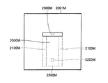
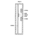
- FIG. 46 is a diagram illustrating an example in which an antenna using the metamaterial 2100B according to the ninth embodiment is applied to a product.
- a case where an antenna using the metamaterial 2100B is applied to a mobile terminal such as a smartphone will be described with reference to FIG.
- the center figure shows the metal casing 2001B in a state where the surface provided with the liquid crystal display on the surface of the portable terminal is opened.
- an antenna using the metamaterial 2100B is formed in the vicinity of the central portion inside the metal casing 2001B.
- the upper right diagram in FIG. 46 shows a state in which the metal casing 2001B in the center diagram is turned over.
- an antenna is formed in the region 2000B of the metal casing 2001B.
- the components for forming antennas, such as metamaterial 2100B are provided inside the metal housing 2001B, they cannot be seen from the outside. For this reason, the design and texture of the metal casing 2001B are not affected.
- FIG. 46 is an enlarged view of a portion where the antenna shown in the center of FIG. 46 is formed. In this state, the feeder line 2200B and the ground plane 2400B are visible.
- the lower left figure in FIG. 46 shows a state in which components for forming the antenna are removed from the metal casing 2001B and viewed from the surface to be bonded to the metal casing 2001B.
- 46 is an enlarged view of a portion including the feeder line 2200B in the lower left diagram of FIG. In this manner, the metamaterial 2100B is arranged outside the region including the feeder line 2200B on the metal housing 2001B side of the ground plane 2400B.
- FIG. 47 is a diagram illustrating an example of a structure for forming an antenna using the metamaterial 2100C according to the tenth embodiment.
- metamaterial 2100C formed of a helical coil is not directly attached to metal flat plate 2001C, but transparent between metamaterial 2100C and metal flat plate 2001C.
- a magnetic body 2700 having a magnetic constant ⁇ 30 is provided.
- one side of the rectangular region 2000C including the feeder line 2200C is a part of one side of the rectangular metal flat plate 2001C, and the other three sides are in contact with the region where the metamaterial 2100C and the magnetic body 2700 are provided. .
- the feed point to which the feed line 2200C is connected is provided in the vicinity of the side of the region 2000C which is a part of one side of the metal flat plate 2001C.
- FIG. 48 is a diagram showing in detail a part of the structure forming the antenna using the metamaterial 2100C according to the tenth embodiment.
- a magnetic body 2700 is provided on the metal plate 2001C side of a metamaterial 2100C formed of a helical coil.
- FIG. 49 is a diagram showing a result of an antenna simulation using the metamaterial 2100C according to the tenth embodiment.
- FIG. 49A shows an electric field distribution of the metal flat plate 2001C.
- FIG. 49B shows the current distribution of the metal flat plate 2001C.
- FIG. 49 (A) and FIG. 49 (B) various resonances are shown only inside the region of the metal flat plate 2001C where the metamaterial 2100C and the magnetic body 2700 are provided, and the metamaterial 2100C and the magnetic body Outside the region of the metal flat plate 2001C where 2700 is provided, a simulation result showing no resonance is obtained. Thus, it will be in the state which cut off a part of metal flat plate 2001C.
- the metamaterial 2100 is attached to a region partitioned by surrounding the entire circumference of the specific region 2000 of the metal casing 2001, thereby the region 2000.
- the region 2000 is explained what works as an antenna.
- FIG. 50 is a diagram for schematically explaining the structure of the antenna using the metamaterial 2100 according to the seventh to ninth embodiments.
- the seventh to ninth embodiments the case where there is a region where the metamaterial 2100 is pasted so as to surround the entire circumference of the specific region 2000 has been described. .
- FIG. 51 is a diagram for schematically explaining the structure of an antenna using the metamaterial 2100D according to the eleventh embodiment.
- the antenna structure using metamaterial 2100D according to the eleventh embodiment two long sides and one short side of specific rectangular region 2000D are pasted by metamaterial 2100. The remaining short side in the vicinity of the feed point to which the feed line 2200 in the region 2000D is connected is connected to the ground plane 2500.
- the ground plane 2500 is connected to the ground 2400D. Even in such a configuration, the region 2000D functions as an antenna.
- the tip is open and the voltage is maximum and current is minimum, and the other is voltage minimum and current maximum. Therefore, the vicinity of the feeding point may be grounded.
- at least one surface is the ground plane 2500, so the amount of the metamaterial 2100D is small. Less cost and cost savings.
- the transmission of electromagnetic waves cannot be completely cut off and cannot be separated electromagnetically. Therefore, if it is dropped to the ground, the blocking efficiency is higher, and it is formed in the region 2000D. This is also advantageous in terms of the characteristics of the antenna used.
- the antenna length needs to be ⁇ / 2. However, if one surface is dropped to the ground, the antenna length can be ⁇ / 4. can do.
- the feeding point may be slightly separated from the ground plane like an inverted F antenna.
- the impedance may be increased by using a structure like a folded monopole antenna.
- FIG. 52 is a diagram for schematically explaining the structure of the antenna using the metamaterial 2100E according to the twelfth embodiment.
- the two long sides of specific rectangular region 2000D are respectively part of the sides of metal flat plate 2001E. Composed. Further, the two short sides of the specific region 2000D are in contact with the region where the metamaterial 2100E is pasted. Even in such a configuration, the region 2000E functions as an antenna.
- the metal flat plate 2001E having the same size as the wavelength, only a part is separated electromagnetically by the metamaterial 2100E, and the separated region 2000E can function as an antenna.
- FIG. 53 is a diagram for schematically explaining the structure of the antenna using the metamaterial 2100F according to the thirteenth embodiment.
- the metamaterial in the antenna structure using metamaterial 2100E in the thirteenth embodiment, the metamaterial is formed such that a specific region 2000F of metal flat plate 2001F is bent like a meander shape. An area to which 2100F is attached is provided. Thereby, the region 2000F functions as an antenna having a longer resonance wavelength (shorter resonance frequency) than when the metal plate 2001F is used as an antenna as it is.
- FIG. 54 is a diagram for schematically explaining the structure of the antenna using the metamaterial 2100G according to the fourteenth embodiment.
- the antenna structure using metamaterial 2100G in the fourteenth embodiment one long side and one short side of a specific rectangular region 2000D are respectively formed on metal plate 2001G. Consists of part of the side. Further, the remaining long side and short side of the specific region 2000D are in contact with the region where the metamaterial 2100E is pasted. Even in such a configuration, the region 2000G functions as an antenna.
- the feeding point can be provided at the end or corner of the metal housing, a part of the entire circumference of the region functioning as the antenna is not the region where the metamaterial is pasted. It doesn't matter.
- the antenna using the metamaterial having one resonance wavelength has been described.
- an antenna using metamaterials having a plurality of resonance wavelengths will be described.
- FIG. 55 is a diagram for explaining the structure of an antenna using metamaterials 2100HA and 2100HB according to the fifteenth embodiment.
- a specific region 2000H is surrounded by a region where metamaterial 2100HA having a resonance frequency of f1 (resonance wavelength is ⁇ 1 ) is attached.
- the resonance frequency f2 in (resonance wavelength lambda 2) attached metamaterials 2100HB an area, to surround the pasted area metamaterial 2100HA.
- a feed point to which the feed line 2200H is connected is provided in the vicinity of the short side of the specific region 2000H.
- the region 2000H can function as an antenna that resonates at both the resonance wavelengths ⁇ 1 and ⁇ 2.
- the specific region 2000H is not limited to being surrounded by a double layer, but may be surrounded by a region to which a metamaterial having more resonance wavelengths is attached.
- the band of the antenna formed in the specific region 2000H can be widened.
- FIG. 56 is a diagram illustrating an example in which an antenna using the metamaterial according to the sixteenth embodiment is applied to a product. With reference to FIG. 56, the case where the antenna using metamaterial 2100KA and 2100KB is applied to portable terminals, such as a smart phone, is demonstrated.
- This figure shows a metal casing 2001K and a non-metal casing 2002K in a state where a surface provided with a liquid crystal display on the surface of the portable terminal is opened. Note that a portion of the casing having the liquid crystal display that is in contact with the metal casing 2001K is also formed of a non-metal.
- the non-metallic material is, for example, resin.
- the areas where the metamaterials 2100KA and 2100KB are attached are provided so that the entire area of the metal casing 2001K is divided into two areas. Thereby, the two short sides of the specific region 2000K including the feed point to which the feed line 2200K is connected are in contact with the region where the metamaterials 2100KA and 2100KB are pasted, and the two long sides are each non-metallic. Touch the housing. Thereby, the specific area 2000K functions as an antenna.
- the entire area of the metal casing 2001K is divided into two areas.
- the entire circumference of the metal casing 2001J is functioned as an antenna without being divided into two regions.
- FIG. 57 is a diagram illustrating an example in which an antenna using the metamaterial according to the seventeenth embodiment is applied to a product.
- metal casing 2001J and nonmetal casing 2002J are the same as metal casing 2001K and nonmetal casing 2002K of the sixteenth embodiment.
- a region to which the metamaterial 2100J is attached is provided at one place in the entire region of the metal casing 2001J.
- the two short sides of the specific region 2000J including the feed point to which the feed line 2200J is connected are in contact with the region to which the metamaterial 2100J is attached, and the two long sides are each a non-metallic housing. Touch.
- the specific area 2000J functions as an antenna.
- the metal casing 2001 in the seventh to ninth embodiments desirably has a thickness less than the skin depth corresponding to the material of the metal casing 2001. This is because if the thickness is greater than the skin depth, the current supplied from the feeder 2200 flows only inside the metal housing 2001 in the region 2000 and does not flow outside the metal housing 2001 in the region 2000. This is because it is difficult to function as an antenna.
- the metal casing 2001 is configured by a metal layer having a thickness less than the skin depth and an insulator layer for maintaining the strength of the metal casing 2001.
- a metal layer having a thickness less than the skin depth is formed by performing metal plating on an insulating layer such as a resin.
- the skin depth value is about 2 ⁇ m for electromagnetic waves having a frequency of 1 GHz in the case of silver, which is a relatively small value among the conductor metals, and increases as the frequency decreases, and copper, gold, aluminum And other metals such as iron are larger than silver.
- the metal layer preferably has a thickness less than the skin depth, but may be thicker than the skin depth as long as the region 2000 can emit an electromagnetic wave necessary for functioning as an antenna. .
- the specific regions 2000E to 2000G, 2000J, and 2000K If the end face is the end face of the metal flat plates 2001E to 2001G and the metal casings 2001J and 2001K, electromagnetic waves can be radiated from the end face, so the thickness of the metal layer may be greater than the skin depth. For this reason, even if the casing is composed of only a metal layer having a thickness capable of maintaining strength, the specific regions 2000E to 2000G, 2000J, and 2000K can function as an antenna.
- the specific region 2000M can function as an antenna.
- FIG. 58 is a view for explaining the structure of an antenna using the metamaterial 2100M according to the eighteenth embodiment.
- two long sides of rectangular specific region 2000M are regions to which metamaterial 2100M is attached, respectively. Touch.
- one of the short sides of the specific region 2000M is in contact with the slit 2900M.
- the other short side in the vicinity of the feed point to which the feed line 2200M in the specific region 2000M is connected is connected to the ground plane 2500M.
- the ground plane 2500M is connected to the ground in the same manner as the ground plane 2500 in FIG. 51 of the eleventh embodiment. Even in such a configuration, the region 2000M functions as an antenna.
- the end surface of the specific region 2000M is exposed on the inner surface of the slit 2900M provided in the metal flat plate 2001M. Since electromagnetic waves can be emitted, the specific region 2000M can function as an antenna.
- At least one surface is not only the grounding surface 2500M, but the other 1 Since the surface is also a slit, the amount of the metamaterial 2100M can be reduced, and the cost can be reduced.
- the ground plane 2500M may not be provided.
- the antenna length of ⁇ / 4 needs to be ⁇ / 2.
- the slit is provided in contact with the short side of the region 2000M. In the nineteenth embodiment, the slit is provided in contact with the long side of the region 2000N.
- FIG. 59 is a view for explaining the structure of the antenna using the metamaterial 2100N according to the nineteenth embodiment.
- the two long sides of specific rectangular region 2000N are in contact with slit 2900N.
- One of the short sides of the region 2000N is in contact with the region where the metamaterial 2100N is attached.
- the other short side in the vicinity of the feed point to which the feed line 2200N in the specific region 2000N is connected is connected to the ground plane 2500N.
- the ground plane 2500N is connected to the ground in the same manner as the ground plane 2500 in FIG. 51 of the eleventh embodiment. Even in such a configuration, the region 2000N functions as an antenna.
- the end surface of the specific region 2000N is exposed on the inner surface of the slit 2900N provided in the metal flat plate 2001N. Since electromagnetic waves can be radiated, the specific region 2000N can function as an antenna.
- the region 2000N functioning as an antenna is entirely surrounded by the region to which the metamaterial is pasted
- at least one surface is not only the ground plane 2500N, but the other two Since the surface is also a slit, the amount of the metamaterial 2100N can be further reduced as compared with the eighteenth embodiment, and the cost can be reduced.
- the slit As compared with the eighteenth embodiment, there are more slits, which is disadvantageous in strength.
- the slit is provided as in the eighteenth embodiment and the nineteenth embodiment, it is preferable to ensure the strength by reinforcing the slit portion with an insulator.
- an inside is an electrical component, it is preferable to provide the structure for waterproofing a slit part.
- the ground plane 2500N may not be provided.
- the antenna length of ⁇ / 4 needs to be ⁇ / 2.
- the metamaterial 2100L is incorporated in advance in a component unit such as the camera unit 2800. Then, when the component unit is attached to a predetermined position of the electric device such as the smartphone 2010, the metamaterial 2100L is a region other than the specific region 2000L where the component of the electromagnetic wave near the resonance wavelength of the metamaterial 2100L is attenuated. It is arranged so as to be formed in a region that divides the region.
- FIG. 60 is a first diagram illustrating an example in which an antenna using the metamaterial 2100L according to the twentieth embodiment is applied to the smartphone 2010.
- smartphone 2010 includes a camera unit 2800. In a state where the camera unit 2800 is attached to the metal casing 2001L, only the lens portion of the camera unit 2800 is outside the metal casing 2001L.
- FIG. 61 is a second diagram illustrating an example in which an antenna using the metamaterial 2100L according to the twentieth embodiment is applied to the smartphone 2010.
- metamaterial 2100L is embedded in the portion of camera unit 2800 that contacts metal casing 2001L when camera unit 2800 is produced.
- FIG. 62 is a third diagram illustrating an example in which the antenna using the metamaterial 2100L according to the twentieth embodiment is applied to the smartphone 2010.
- the camera unit 2800 is attached to the metal casing 2001L.
- FIG. 63 is a fourth diagram illustrating an example in which the antenna using the metamaterial 2100L according to the twentieth embodiment is applied to the smartphone 2010.
- metal casing 2001L where metamaterial 2100L is in contact
- metal casing 2001L through which the lens of camera unit 2800 penetrates.
- the specific region 2000L surrounded by the holes is electromagnetically separated.
- a power supply line is connected near the lower end in the drawing of the specific region 2000L.
- a grounding portion may be provided at the lower end in the drawing of the specific region 2000L.
- the separated specific area 2000L functions as an antenna.
- a hole is originally formed in a portion to which the camera unit 2800 of the metal casing 2001L is attached, and a specific region 2000L is defined by the hole and the metamaterial 2100L previously incorporated in the camera unit 2800. Can be separated electromagnetically and can function as an antenna. For this reason, an antenna can be easily formed in a part of the metal casing 2001L using a hole or a slit for attaching a device such as the camera unit 2800 of a mobile terminal such as the smartphone 2010.
- a metamaterial may be incorporated in the component unit in advance.
- the metamaterial forms a region that blocks the electromagnetic wave component near the resonance wavelength of the metamaterial in a region that partitions the specific region from the other region. If it arrange
- the feeder line is connected to a specific area defined by the metamaterial or the outline of the flat plate so as to function as an antenna.
- the power supply line is not connected to a specific region defined by the metamaterial or the flat plate contour, but functions as an electric window.
- FIG. 64 is a diagram for explaining the structure of an electric window using the metamaterial 2100P according to the twenty-first embodiment.
- FIG. 64A is a plan view.
- FIG. 64B is a side view. Referring to FIGS. 64A and 64B, a plurality of metamaterials 2100P are pasted on the inner surface of metal casing 2001P in a region that divides region 2000P to be functioned as an electric window from other regions. It is done.
- the region of the metal casing 2001P to which the metamaterial 2100P is attached largely blocks the electromagnetic wave component equivalent to the high impedance region with respect to the electromagnetic wave component near the resonance wavelength of the metamaterial 2100P. Or, it is a region that substantially blocks the electromagnetic wave component. For this reason, the region 2000P is separated from other regions in resonance with the resonance wavelength component of the electromagnetic field.
- the region 2000 is electromagnetically separated from other regions, and a component in the vicinity of the resonance wavelength of the metamaterial 2100P of the electromagnetic field. It functions as an electrical window that resonates with the electromagnetic wave and emits the electromagnetic wave having the wavelength of the electromagnetic wave incident from the inner surface from the outer surface.
- part of the metal casing 2001P can function as an electric window. That is, even if the entire surface of the metal casing 2001P is metal, the antenna can be mounted inside the metal casing 2001P.
- FIG. 65 is a diagram for explaining the function of the electric window using the metamaterial 2100P according to the twenty-first embodiment.
- FIG. 65A shows the progress of electromagnetic waves in the case of a conventional metal casing 5001.
- FIG. 65B shows the progress of electromagnetic waves in the case of the electric window of the present embodiment.
- electromagnetic waves cannot pass through the metal casing 5001.
- electromagnetic waves can pass through the portion of the electric window in region 2000P of metal casing 2001P.
- FIG. 66 is a diagram illustrating an example in which an electric window using the metamaterial 2100Q according to the twenty-second embodiment is applied to a product. Referring to FIG. 66, by attaching metamaterial 2100Q to the inside of metal casing 2001Q, region 2000Q that functions as an electrical window is formed. A plurality of antennas 2600 are provided on the internal circuit board 2300Q.
- the electromagnetic waves radiated from the plurality of antennas 2600 respectively pass through the electric window in the region 2000Q.
- the electromagnetic wave cannot pass through the metal casing 2001Q other than the electric window portion in the region 2000Q.
- a plurality of antennas can be provided inside the metal casing 2001Q.
- antenna 2600 the antenna by the wiring on a chip antenna and a printed circuit board can be used, for example. Therefore, when a plurality of antennas are provided, space can be saved and manufacturing cost can be reduced.
- the antenna has a long history, and there are many known technologies such as monopole, dipole, helical, and inverse F. There is also a chip-type antenna using ceramics (see Japanese Patent Application Laid-Open No. 9-162525).
- antennas are installed inside the housing for reasons of miniaturization, heat dissipation, and design. Therefore, a resin that allows radio waves to pass through is used for the housing.
- the top end of the housing on the liquid crystal display side is made of resin and an antenna is installed there. Therefore, since strength can be ensured compared with the case where the whole is made of resin, it can be made thinner.
- a 1-segment partial reception service for mobile phones / mobile terminals a so-called mono-segment antenna for receiving one-segment broadcasting, is provided outside the device as a telescopic rod type.
- the antenna of a mobile phone is often configured on a printed circuit board.
- the chip antenna is mounted on the substrate.
- FIG. 75 is a diagram showing the arrangement of the conventional antenna 3000 when the case 3001 is made of resin.
- antenna 3000 when antenna 3000 is formed on a substrate 3300 such as a cellular phone, there is no problem because radio waves can be transmitted if case 3001 outside the cellular phone is made of resin.
- FIG. 76 is a diagram showing a case where the case 4001 is made of metal. Referring to FIG. 76, when case 4001 is made of metal or conductive resin, it does not transmit radio waves. Therefore, even if antenna 4000 is formed on internal substrate 4300, it functions as antenna 4000. I can't.
- the antenna described in the above-mentioned Japanese Patent Laid-Open No. 9-162525 cannot function as an antenna when formed inside a case that does not transmit radio waves.
- FIG. 77 is a diagram showing a case where a part of the case 4002 of the metal case 4001 is formed of resin.
- the case 4001 does not transmit radio waves
- a portion of the case 4002 of the metal case 4001 is made of resin that transmits radio waves so that the radio waves are not blocked.
- a part of a metal top plate is made of resin, and an antenna is formed there.
- FIG. 78 is a diagram showing a case where the antenna 4100 is arranged outside the metal case 4001. Referring to FIG. 78, when case 4001 does not transmit radio waves, as a second method, antenna 4100 is provided outside the device.
- the antenna 4100 is attached to the outside of the device, there is no problem in the function of the antenna 4100. However, in that case, there is a problem that the antenna 4100 does not meet the needs of consumers because the antenna 4100 may be in the way or it may be troublesome to put out the antenna 4100. For this reason, a built-in antenna is still desired.
- the antenna since the portion to be replaced with resin can be minimized, the antenna must be mounted in a narrow space, and a small antenna is required, which may sacrifice the gain.
- wireless communication standards such as W-LAN, Bluetooth (registered trademark), and WiMAX (registered trademark) (Worldwide Interoperability for Microwave Access) are increasing, and the number of antennas that must be installed in wireless devices has increased. continuing.
- LTE Long Term Evolution
- a notebook PC with a metal casing as described above has a problem that a space for mounting an antenna cannot be secured.
- the above-described problems can be solved and a part of the flat plate having the conductive layer can function as an antenna.
- the feeder line is connected to a specific area defined by the metamaterial or the outline of the flat plate so as to function as an antenna.
- the feeder line is connected to a specific area defined by the metamaterial and the slit so as to function as an antenna.
- a feed line is connected to a specific area defined by the slit so as to function as an antenna.
- FIG. 67 is a view for explaining the structure of the antenna using the slit 2900R according to the twenty-third embodiment.
- a U-shaped slit 2900R is provided on a metal flat plate 2001R.
- a specific region 2000R is partitioned inside the U-shape.
- the shape of the specific region 2000R is a shape in which the specific region 2000R functions as an antenna by supplying power to the specific region 2000R (in this embodiment, the shape of a rectangular monopole antenna).
- a ground is provided around the side connected to the other region of the metal flat plate 2001R of the specific region 2000R.
- the shape of the specific region 2000R is not limited to the shape of a rectangular monopole antenna, and may be other antenna shapes such as a dipole antenna shape as long as it functions as an antenna.
- a specific area 2000R of the part of the housing of the electrical product can be used as an antenna as it is. This eliminates the need for an existing external antenna and an antenna provided inside a part of the metal casing made of resin.
- the antenna can be formed by punching and molding the slits of the metal casing without the need to bond the metal and the resin as in the case where a part of the metal casing is made of resin. For this reason, not only manufacturing is simplified, but also manufacturing costs can be reduced.
- the slits do not need to be hollowed out around the antenna shape and may be grounded on one side, and may be U-shaped as in this embodiment. If it is U shape, the intensity
- the U-shaped slit, including a dummy that is not used as an antenna, can be designed not only as an antenna but also as a design if it is placed in a periodic pattern. It is possible to maintain the aesthetic appearance by providing the slit.
- the radiation efficiency is close when compared with the same size. It is lower than a normal antenna without ground.
- an antenna is incorporated in the resin casing portion at the tip of the display-side casing. Compared with this, an antenna using a slit is formed on a metal surface. For example, since a large area can be used, the antenna size can be increased. As a result, there is an advantage that radiation efficiency is improved.
- the metal plate 2001R is located near the specific region 2000R that functions as an antenna, so the gain as the antenna is reduced, but the antenna is formed on the same surface as the housing. Therefore, significant space saving can be achieved.
- the slit 2900R is basically a metal casing, so that the strength is higher than that of a conventional resin casing, and the product can be made thinner.
- a feeding line is connected to a specific area defined by a slit so as to function as an antenna.
- a feeder line is connected to a specific area defined by the outline of the slit and the metal flat plate so as to function as an antenna.
- FIG. 68 is a view for explaining the structure of the antenna using the slit 2900S according to the twenty-fourth embodiment.
- an L-shaped slit 2900S connected to the end of the metal flat plate 2001S is provided in the metal flat plate 2001S.
- a specific region 2000S is defined by the L-shaped slit 2900S and the end of the metal flat plate 2001S.
- the shape of the specific region 2000S is a shape in which the specific region 2000S functions as an antenna by supplying power to the specific region 2000S (in the present embodiment, the shape of a rectangular monopole antenna).
- a ground is provided around the side connected to the other region of the metal flat plate 2001S of the specific region 2000S.
- the shape of the specific region 2000S is not limited to the shape of a rectangular monopole antenna, and may be other antenna shapes such as a dipole antenna shape as long as it functions as an antenna.
- the following effects can be obtained. Since the end portion of the metal flat plate 2001S is used, the number of locations that can function as an antenna is reduced as compared with the case of the twenty-third embodiment in which the entire surface of the metal flat plate 2001R can be used. The slit when forming the film can be short, and the mechanical strength can be increased.
- the antenna is formed using the surface of the metal flat plate 2001R, and in the twenty-fourth embodiment, the antenna is formed using the side of the metal flat plate 2001S. Similarly, you may make it form an antenna using the corner of a metal flat plate.
- FIG. 69 is a diagram for explaining the structure of the antenna using the slit 2900T according to the twenty-fifth embodiment.
- a slit 2900T connected to a mounting hole of camera unit 2800T of metal casing 2001T is provided in metal casing 2001T. This corresponds to the side of the metal flat plate 2001S according to the twenty-fourth embodiment being around a hole in the surface of the metal casing 2001T.
- a specific region 2000T is defined by the slit 2900T and the mounting hole of the camera unit 2800T.
- the shape of the specific region 2000T is a shape in which the specific region 2000T functions as an antenna by supplying power to the specific region 2000T (in this embodiment, the shape of a monopole antenna).
- a ground is provided around the side connected to the other region of the metal casing 2001T in the specific region 2000T.
- the shape of the specific region 2000T is not limited to the shape of the monopole antenna, and may be the shape of another antenna such as the shape of a dipole antenna as long as it functions as an antenna.
- the shape of the specific region 2000T functioning as an antenna is an arc shape, and can be an ideal shape as an antenna.
- the camera unit 2800T is adhered to the specific region 2000T so that the mechanical unit 2800T adheres to the structure so that the specific region 2000T is supported from the back side, thereby improving the mechanical strength of the specific region 2000T. it can.
- FIG. 70 is a view for explaining the structure of the antenna using the slit 2900U according to the twenty-sixth embodiment.
- 71 is a diagram showing an arrow AA in FIG.
- FIG. 72 is a perspective view of the structure of the antenna using the slit 2900U according to the twenty-sixth embodiment.
- a U-shaped slit 2900U is provided on the metal flat plate 2001U in the same manner as described in FIG. 67 of the twenty-third embodiment.
- a specific region 2000U is partitioned inside the U-shape.
- the shape of the specific region 2000U is such a shape that the specific region 2000U functions as an antenna by supplying power to the specific region 2000U (in this embodiment, the shape of a rectangular monopole antenna).
- the printed board 2750 is attached from the back side of the metal flat plate 2001U so as to close the slit 2900U.
- This printed circuit board 2750 is provided with a power supply line 2200U for supplying power to a specific region 2000U and a ground electrode 2400U connected to the ground of the power supply line 2200U in advance.
- the ground electrode 2400U is electrically connected to the side connected to the other region of the metal flat plate 2001U in the specific region 2000U.
- the impedance matching of the antenna in the specific area 2000U can be adjusted.
- the resonance frequency of the antenna in the specific region 2000U can be adjusted.
- the shape of the specific region 2000U is not limited to the shape of the rectangular monopole antenna, and may be other antenna shapes such as the shape of a dipole antenna as long as the shape functions as an antenna.
- the following effects are obtained.
- the slit 2900U is formed by punching, it is difficult to finely adjust the size of the slit 2900U because it is performed using a mold.
- the antenna in the specific region 2000U has the same slit 2900U shape, and the resonance frequency changes slightly due to the influence of the internal dielectric constant and metal distribution, so fine adjustment is usually required.
- impedance matching and resonance frequency can be changed by changing the circuit board. Adjustment is possible.
- the printed circuit board 2750 is attached so as to close the slit 2900U from the back side of the slit 2900U, the mechanical strength of the specific region 2000U can be reinforced.
- the printed board 2750, the ground electrode 2400U, and the power supply line 2200U for reinforcing the slit 2900U may be formed integrally as in the present embodiment, or may be formed separately.
- portion of the slit 2900U may be filled with an insulating adhesive resin or the like instead of the above-described printed board 2750 or together with the printed board 2750.
- FIG. 73 is a diagram for explaining a case where a plurality of conventional slot antennas 5900 are provided on the same metal flat plate 6001. Referring to FIG. 73, slot antenna 5900 generates an electromagnetic field in the slot. However, current flows around the slot and couples when there are multiple slot antennas 5900.
- FIG. 74 is a diagram for explaining a case where a plurality of antennas using the slits 2900V according to the twenty-seventh embodiment are provided on the same metal flat plate 2001V.
- a specific region 2000V that functions as a monopole antenna separated by a plurality of slits 2900V current concentrates in each separated specific region 2000V, so that even if there are a plurality of antennas, coupling is performed. do not do.
- the following effects can be obtained.
- the area where the antenna can be installed is increased, and a plurality of antennas can be provided on the entire surface of the metal flat plate 2001V constituting the metal casing. The number of installed can be increased.
- a slit is provided in contact with a specific area, and electromagnetic waves can be radiated from the slit portion.
- the thickness of the metal layer may be greater than the skin depth.
- the method using a coil and a magnetic material aims to increase the impedance Z by increasing the magnetic permeability ⁇ in addition to lowering the dielectric constant ⁇ .
- YIG Yttrium Iron Garnet
- YIG has a problem that the Q value is not high and a magnet is required.
- the impedance can be increased as compared with the method using a coil. Further, in the method using the coil and the magnetic body, there is no suitable material that can be used in the GHz band, but according to the structure of the metamaterial 2100W according to the twenty-eighth embodiment, the impedance can be increased.
- FIG. 79 is a diagram for explaining a structure for electrically cutting off the metal line 2001W using the metamaterial 2100W according to the twenty-eighth embodiment.
- FIG. 80 is a side view of a structure for electrically blocking the metal line 2001W using the metamaterial 210W according to the twenty-eighth embodiment.
- FIG. 81 is a front view of a structure for electrically blocking metal line 2001W using metamaterial 2100W according to the twenty-eighth embodiment.
- FIG. 82 is a trihedral view showing details of the upper stage portion of the structure for electrically blocking the metal line 2001W using the metamaterial 2100W according to the twenty-eighth embodiment.
- FIG. 83 is a three-view drawing showing details of the lower part of the structure for electrically blocking the metal line 2001W using the metamaterial 2100W according to the twenty-eighth embodiment.
- the upper part and the lower part are each configured to express a positive magnetic permeability greater than 1 and a dielectric constant whose absolute value is less than 1, or less than ⁇ 1 It is configured to develop a negative magnetic permeability and a dielectric constant having an absolute value of less than 1.
- the metal line 2001W can be electrically interrupted
- the dielectric constant having an absolute value of less than 1 includes a case where the dielectric constant is zero.
- a ground 2400W is provided on the opposite side of the metal line 2001W across the metamaterial 2100W.
- lower stage portion 2102 ⁇ / b> W includes uppermost electrode 2110 a, first via 2112 a, second via 2112 b, lowermost electrode 2110 b, and line 2140.
- the first via 2112a, the line 2140, and the second via 2112b connect the uppermost electrode 2110a and the lowermost electrode 2110b.
- the total length of the first via 2112a, the line 2140, and the second via 2112b is approximately 1 ⁇ 4 of the resonance wavelength.
- the first via 2112a, the line 2140, and the second via 2112b function as part of the ⁇ / 4 line, and realize a dielectric constant having an absolute value of less than 1.
- the shape of the line 2140 is not limited to the meander line shown in the figure, and may be helical or spiral, for example.
- the uppermost electrode 2110a and the lowermost electrode 2110b exhibit a function of reducing the absolute value of the dielectric constant to less than 1 and shortening the resonance wavelength. However, the uppermost electrode 2110a and the lowermost electrode 2110b can be omitted.
- the lowermost electrode 2110b is electrically connected to the ground 2400W.
- the resonance of ⁇ / 4 is used as the ⁇ / 4 line, it is electrically connected to the ground 2400W.
- the coil becomes long, but it is not necessary to connect to the ground 2400W, so the manufacturing process is simplified.
- the size of the lower step 2102W is 3.2 mm in width, 3.4 mm in depth, and 1.5 mm in height.
- the structure of the lower step 2102W is a structure in which five resonators of this size are connected in the width direction.
- Lower step 2102W is made of, for example, a resin substrate.
- upper stage portion 2101W includes a first internal electrode 2122, a second internal electrode 2124a, a third internal electrode 2124b, a fourth internal electrode 2130, and a third via 2150. , And a fourth via 2160.
- the third via 2150 connects the second internal electrode 2124a and the fourth internal electrode 2130.
- the fourth via 2160 connects the third internal electrode 2124b and the fourth internal electrode 2130.
- the second internal electrode 2124a, the third via 2150, the third internal electrode 2124b, the fourth via 2160, and the fourth internal electrode 2130 have a structure similar to that of the split ring resonator, and are negative It functions as a resonator that exhibits magnetic permeability or positive magnetic permeability.
- the first internal electrode 2122 compensates for the capacitance of the cut portion between the second internal electrode 2124a and the third internal electrode 2124b, similarly to the first internal electrode 722 of the fourth embodiment. It plays a role of lowering the resonance frequency.
- the upper stage 2101W has a width of 2.4 mm, a depth of 2.0 mm, and a height of 1.8 mm. Five resonators of this size are respectively disposed on the resonators of the lower stage 2102W.
- the upper step 2101W is made of, for example, a ceramic multilayer substrate.
- the resonator of the upper stage 2101W is an LC resonator, and functions as an artificial magnetic body at the resonance point. Because of resonance, there is a demerit that the frequency band that can be used as a magnetic material is narrow, but there is an advantage that it can also be used in the GHz band.
- the LC resonator has an anisotropy in a general configuration and has a demerit that it resonates only with a magnetic field in a specific direction. For this reason, although it is difficult to apply to a flat plate having a relatively small aspect ratio, there is no problem if it is used for a line-shaped metal having a relatively large aspect ratio and a relatively narrow width like the metal line 2001W.
- the length of the metal line 2001W is not limited, and a part of the metal line 2001W can be an antenna that resonates at a desired frequency.
- the metal line 2001W is used as a multimode antenna that resonates only at a frequency corresponding to ⁇ / 4, 3 ⁇ / 4, 5 ⁇ / 4,...,
- Resonance at an arbitrary frequency can be newly added without significantly affecting the resonating frequency. For this reason, it can be set as the antenna corresponding to arbitrary frequencies in addition to the original resonant frequency.
- a plurality of (in this case, five) metamaterial units are arranged is to cover a plurality of phases.
- the number of units is not limited to five as long as a plurality of phases can be covered.
- the upper stage 2101W is separated.
- the present invention is not limited to this, and may be integrated.
- the upper step portion 2101W and the lower step portion 2102W are bonded together.
- the present invention is not limited to this, and the upper step portion 2101W and the lower step portion 2102W are manufactured integrally. May be.
- FIG. 84 is a diagram for explaining the structure of the metamaterial 2100X according to the twenty-ninth embodiment.
- FIG. 85 is a three-view drawing of the metamaterial 2100X according to the twenty-ninth embodiment.
- the metamaterial 2100X is obtained by changing the metamaterial 2100W of the 28th embodiment from five to three.
- the structures of the upper stage 2101X and lower stage 2102X of each unit of the metamaterial 2100X and the positional relationship between the metamaterial 2100X, the metal frame 2001X, and the ground 2400X are the same as those in the twenty-eighth embodiment, and thus overlap. The explanation will not be repeated.
- FIG. 86 is a plan view schematically showing a state in which the metamaterial 2100X according to the 29th embodiment is mounted on a smartphone.
- FIG. 87 is a perspective view schematically showing a state in which the metamaterial 2100X according to the 29th embodiment is mounted on a smartphone.
- the smartphone includes a metal frame 2001X and a ground substrate 2410X.
- the metal frame 2001X and the ground substrate 2410X are electrically connected.
- the metamaterial 2100X described in FIG. 84 and FIG. 85 is mounted so that the upper stage portion 2101X is brought close to the metal frame 2001X side and blocks components near the resonance wavelength of the metamaterial 2100X of the current flowing through the metal frame 2001X. Is done.
- the ground 2400X is electrically connected to the ground substrate 2410X, and is disposed close to the lower step portion 2102X side of the metamaterial 2100X.
- the ground 2400X is preferably longer than the metamaterial 2100X.
- the blocking of electromagnetic waves uses the increase in impedance due to the metamaterial 2100X. For this reason, if the ground 2400X is made longer than the metamaterial 2100X and the impedance near the metamaterial 2100X is lowered, the impedance difference becomes larger and the blocking effect becomes larger.
- the feeder line 2200X is connected to a specific region 2000X from the region where the metamaterial 2100X of the metal frame 2001X is brought close to the portion connected to the ground substrate 2410X and grounded.
- the specific region 2000X functions as an antenna having a frequency corresponding to the vicinity of the resonance wavelength.
- metal frames or bars may be used mainly for design purposes on the side or surface of devices such as mobile phones and PCs equipped with antennas. In that case, there is a demand for using them as antennas.
- the resonance frequency is determined by the physical length of the metal frame or bar. For this reason, since it is necessary to give priority to the design as a product, it is difficult to use a metal frame or bar as an antenna.
- a physical slit can be provided in the metal frame to function as an antenna.
- a physical slit can be provided in the metal frame to function as an antenna.
- the lower stage 2102X can lower the apparent dielectric constant ⁇ at the resonance frequency, and the upper stage Since the apparent permeability ⁇ can be increased by 2101X, the impedance can be increased.
- a plurality of metamaterials 2100X may be installed to electrically separate a plurality of locations. Thereby, a plurality of antennas can be formed on one metal frame 2001X.
- portable terminals such as a smart phone
- portable terminals such as a smart phone
- an antenna using a metamaterial or an apparatus using a slit without using a metamaterial has a metal outer plate (for example, a housing, a body, etc.) and is mounted on the antenna. Any electrical device that is necessary may be used.
- it may be an electric device such as a portable terminal, PC, video, TV, refrigerator or air conditioner, a transport device such as an automobile or a train, or a building equipment such as a door for an electric lock house.
- the external antenna can be eliminated, and the outer plate can be made entirely of metal, so that it is possible to realize a product that does not impair rigidity and a beautiful texture.
- an antenna using a metamaterial or an antenna using a slit without using a metamaterial is provided inside a car roof or bonnet
- the conventional antenna is used.
- the elimination of extraneous external components is advantageous in terms of air resistance and design.
- an antenna embedded in the glass surface is not preferred by the user because it enters the user's field of view, but according to the present embodiment, it is not necessary to embed the antenna in the glass surface. . It can also be applied to keyless entry.
- the twelfth embodiment is different from the twelfth embodiment.
- the end surface of the specific area is also a metal flat plate or an end surface of a metal housing, As described from the embodiment to the twentieth embodiment and from the twenty-third embodiment to the twenty-seventh embodiment, if the end surface of the specific region is exposed on the inner surface of the slit, An electromagnetic wave can be emitted from the antenna.
- the present invention can also be applied to a side panel of a desktop PC, such as a back panel of a thin PC such as a notebook PC and a slate PC, or a liquid crystal back panel, and a PC equipped with MIMO (Multiple Input Multiple Output).
- a side panel of a desktop PC such as a back panel of a thin PC such as a notebook PC and a slate PC, or a liquid crystal back panel, and a PC equipped with MIMO (Multiple Input Multiple Output).
- MIMO Multiple Input Multiple Output
- a metal frame as a multiband antenna was shown.
- a cable used for wiring as an antenna. Since the cable is low-cost and flexible, it is optimal as an antenna wire. However, the cable functions only as a monopole antenna and cannot support multiband. For this reason, there have been few examples that have been used as antennas. However, if a metamaterial is used, a resonance frequency can be freely added. As a result, the cable can be used as a multi-antenna.
- the antenna function can be added using the metal casing without demetalization.
- the antenna has both a metal part and a non-metal part, since the thing like the glass embedded antenna of a motor vehicle as mentioned above attaches importance to appearance and a function, it can be mounted in a metal part.
- the antenna is mounted inside, what is currently a non-metal casing can be advantageous in terms of appearance and strength by forming a metal casing and configuring the antenna function in the metal casing. .
- the strength of the antenna can be increased and the size of the device can be reduced.
- the resonance frequency fluctuates even if the specific area that functions as the antenna is partitioned by the area where the metamaterial is pasted. It does n’t happen.
- a feeding point is provided in a specific region, and the electromagnetic wave component equivalent to the high impedance region with respect to the component near the resonance wavelength of the current fed from the feeding point is largely blocked.
- the specific region is made an antenna. It was made to function as.
- the specific region is not limited to the one that functions as an antenna.
Landscapes
- Engineering & Computer Science (AREA)
- Computer Networks & Wireless Communication (AREA)
- Details Of Aerials (AREA)
Abstract
L'invention concerne un appareil électrique comprenant une partie (2001X) munie d'une couche conductrice située dans une plage prédéterminée dans le sens de la profondeur. La couche conductrice comprend une région pour réaliser le blindage électromagnétique d'une région spécifique dans la couche conductrice par rapport aux autres régions. L'appareil électrique comprend en outre un métamatériau (2100X) qui peut présenter une permittivité inférieure à 1 en valeur absolue et une perméabilité supérieure à 1 en valeur absolue, par rapport à une longueur d'onde de résonance prédéterminée du champ électromagnétique. Le métamatériau est disposé de telle sorte qu'une région de coupure pour couper les composantes de longueur d'onde de résonance proches d'un courant qui circule dans la couche conductrice est formée au niveau d'une région de cloisonnement destinée à cloisonner la région spécifique (2000X) de la couche conductrice par rapport aux autres régions. Au moins une partie de la région spécifique peut rayonner des ondes électromagnétiques. La région spécifique peut être isolée électromagnétiquement des autres régions.
Priority Applications (2)
| Application Number | Priority Date | Filing Date | Title |
|---|---|---|---|
| JP2012556856A JP5482915B2 (ja) | 2011-02-10 | 2012-02-03 | メタマテリアル、電気装置、および、メタマテリアルを備えた電気装置 |
| US13/961,997 US20130321220A1 (en) | 2011-02-10 | 2013-08-08 | Metamaterial, electric apparatus, and electric apparatus including metamaterial |
Applications Claiming Priority (4)
| Application Number | Priority Date | Filing Date | Title |
|---|---|---|---|
| JP2011027484 | 2011-02-10 | ||
| JP2011-027484 | 2011-02-10 | ||
| JP2011044838 | 2011-03-02 | ||
| JP2011-044838 | 2011-03-02 |
Related Child Applications (1)
| Application Number | Title | Priority Date | Filing Date |
|---|---|---|---|
| US13/961,997 Continuation US20130321220A1 (en) | 2011-02-10 | 2013-08-08 | Metamaterial, electric apparatus, and electric apparatus including metamaterial |
Publications (1)
| Publication Number | Publication Date |
|---|---|
| WO2012108351A1 true WO2012108351A1 (fr) | 2012-08-16 |
Family
ID=46638567
Family Applications (1)
| Application Number | Title | Priority Date | Filing Date |
|---|---|---|---|
| PCT/JP2012/052498 Ceased WO2012108351A1 (fr) | 2011-02-10 | 2012-02-03 | Métamatériau, appareil électrique et appareil électrique équipé d'un métamatériau |
Country Status (3)
| Country | Link |
|---|---|
| US (1) | US20130321220A1 (fr) |
| JP (1) | JP5482915B2 (fr) |
| WO (1) | WO2012108351A1 (fr) |
Cited By (5)
| Publication number | Priority date | Publication date | Assignee | Title |
|---|---|---|---|---|
| EP2784875A1 (fr) * | 2013-03-29 | 2014-10-01 | Fujitsu Limited | Antenne et appareil de communication sans fil |
| CN106033845A (zh) * | 2015-03-20 | 2016-10-19 | 深圳光启高等理工研究院 | 超材料及超材料的导电微结构制作方法 |
| JP2018137557A (ja) * | 2017-02-20 | 2018-08-30 | 学校法人 龍谷大学 | 人工誘電体及び人工誘電体共振器 |
| JPWO2018079305A1 (ja) * | 2016-10-24 | 2019-09-12 | 日本精機株式会社 | 携帯型通信装置 |
| JP2020182107A (ja) * | 2019-04-25 | 2020-11-05 | 地方独立行政法人大阪産業技術研究所 | 電子部材およびその製造方法 |
Families Citing this family (8)
| Publication number | Priority date | Publication date | Assignee | Title |
|---|---|---|---|---|
| TWI565400B (zh) * | 2014-07-01 | 2017-01-01 | 華碩電腦股份有限公司 | 電磁帶隙結構與具有電磁帶隙結構的電子裝置 |
| JP6402774B2 (ja) * | 2014-10-16 | 2018-10-10 | 株式会社村田製作所 | アンテナモジュール収納構造 |
| TW201644096A (zh) * | 2015-06-01 | 2016-12-16 | 華碩電腦股份有限公司 | 人工磁導結構及其電子裝置 |
| CN106450787A (zh) * | 2015-08-11 | 2017-02-22 | 广东格林精密部件股份有限公司 | 一种全封闭金属框架作反射器的移动设备天线设计方法 |
| US10097031B2 (en) | 2016-09-20 | 2018-10-09 | Hong Kong Applied Science And Technology Research Insittute Company Limited | Charging device having small loop transmission coils for wireless charging a target device |
| US11037765B2 (en) * | 2018-07-03 | 2021-06-15 | Tokyo Electron Limited | Resonant structure for electron cyclotron resonant (ECR) plasma ionization |
| US20230102508A1 (en) * | 2020-01-24 | 2023-03-30 | Jyri Kaija | Functional Housing Structure for an Electronic Device |
| JP2021135850A (ja) * | 2020-02-28 | 2021-09-13 | レノボ・シンガポール・プライベート・リミテッド | 電子機器 |
Citations (5)
| Publication number | Priority date | Publication date | Assignee | Title |
|---|---|---|---|---|
| WO2009081663A1 (fr) * | 2007-12-21 | 2009-07-02 | Murata Manufacturing Co., Ltd. | Filtre d'élimination de bande et connecteur doté de ce filtre |
| WO2009128310A1 (fr) * | 2008-04-18 | 2009-10-22 | 株式会社村田製作所 | Substrat fonctionnel |
| WO2010026907A1 (fr) * | 2008-09-03 | 2010-03-11 | 株式会社村田製作所 | Metamateriau |
| JP2010103609A (ja) * | 2008-10-21 | 2010-05-06 | Olympus Corp | 電磁波伝搬媒質 |
| WO2010125784A1 (fr) * | 2009-04-30 | 2010-11-04 | 日本電気株式会社 | Corps structurel, carte de circuit imprimé, antenne, convertisseur guide d'ondes de ligne de transmission, antenne réseau, et dispositif électronique |
-
2012
- 2012-02-03 JP JP2012556856A patent/JP5482915B2/ja active Active
- 2012-02-03 WO PCT/JP2012/052498 patent/WO2012108351A1/fr not_active Ceased
-
2013
- 2013-08-08 US US13/961,997 patent/US20130321220A1/en not_active Abandoned
Patent Citations (5)
| Publication number | Priority date | Publication date | Assignee | Title |
|---|---|---|---|---|
| WO2009081663A1 (fr) * | 2007-12-21 | 2009-07-02 | Murata Manufacturing Co., Ltd. | Filtre d'élimination de bande et connecteur doté de ce filtre |
| WO2009128310A1 (fr) * | 2008-04-18 | 2009-10-22 | 株式会社村田製作所 | Substrat fonctionnel |
| WO2010026907A1 (fr) * | 2008-09-03 | 2010-03-11 | 株式会社村田製作所 | Metamateriau |
| JP2010103609A (ja) * | 2008-10-21 | 2010-05-06 | Olympus Corp | 電磁波伝搬媒質 |
| WO2010125784A1 (fr) * | 2009-04-30 | 2010-11-04 | 日本電気株式会社 | Corps structurel, carte de circuit imprimé, antenne, convertisseur guide d'ondes de ligne de transmission, antenne réseau, et dispositif électronique |
Cited By (5)
| Publication number | Priority date | Publication date | Assignee | Title |
|---|---|---|---|---|
| EP2784875A1 (fr) * | 2013-03-29 | 2014-10-01 | Fujitsu Limited | Antenne et appareil de communication sans fil |
| CN106033845A (zh) * | 2015-03-20 | 2016-10-19 | 深圳光启高等理工研究院 | 超材料及超材料的导电微结构制作方法 |
| JPWO2018079305A1 (ja) * | 2016-10-24 | 2019-09-12 | 日本精機株式会社 | 携帯型通信装置 |
| JP2018137557A (ja) * | 2017-02-20 | 2018-08-30 | 学校法人 龍谷大学 | 人工誘電体及び人工誘電体共振器 |
| JP2020182107A (ja) * | 2019-04-25 | 2020-11-05 | 地方独立行政法人大阪産業技術研究所 | 電子部材およびその製造方法 |
Also Published As
| Publication number | Publication date |
|---|---|
| JP5482915B2 (ja) | 2014-05-07 |
| US20130321220A1 (en) | 2013-12-05 |
| JPWO2012108351A1 (ja) | 2014-07-03 |
Similar Documents
| Publication | Publication Date | Title |
|---|---|---|
| JP5482915B2 (ja) | メタマテリアル、電気装置、および、メタマテリアルを備えた電気装置 | |
| TWI686009B (zh) | 多天線及具備其之無線裝置 | |
| US9077081B2 (en) | Multi-antenna device and communication apparatus | |
| CN110176670B (zh) | 具有用于处理近场通信和非近场通信的隙缝的电子设备 | |
| US10741909B2 (en) | Electronic devices having multi-band slot antennas | |
| JP5641166B2 (ja) | アンテナ装置及びそれを備える無線装置 | |
| CN116345145B (zh) | 可折叠电子设备及其天线系统 | |
| US20190165466A1 (en) | Antenna system | |
| US7932869B2 (en) | Antenna with volume of material | |
| CN113328233A (zh) | 电子设备 | |
| TW202141851A (zh) | 天線結構及具有該天線結構之電子設備 | |
| WO2011090080A1 (fr) | Dispositif à antenne et appareil terminal de communication | |
| JP2011082985A (ja) | 電磁フィルタ装置および当該電磁フィルタ装置を備える電子機器 | |
| WO2014034587A1 (fr) | Dispositif d'antenne, et dispositif de terminal de communication | |
| JP5381463B2 (ja) | アンテナとそれを有する通信装置 | |
| JP5969821B2 (ja) | アンテナ装置 | |
| KR20100042704A (ko) | 미모 안테나 장치 | |
| US9306277B2 (en) | Multi-antenna device and communication device | |
| KR101018628B1 (ko) | 다중 대역 안테나 장치 및 이를 이용한 통신 장치 | |
| CN113809517A (zh) | 天线装置与电子设备 | |
| JP5900660B2 (ja) | Mimoアンテナおよび無線装置 | |
| JP2014120989A (ja) | 入力装置、および、その入力装置を備えた電気機器 | |
| JP6865072B2 (ja) | アンテナ装置及びアンテナ装置を備えた電子機器 | |
| WO2014203967A1 (fr) | Dispositif d'antenne et dispositif sans fil équipé de ce dernier | |
| WO2014027457A1 (fr) | Élément de suppression de courant et procédé de suppression de courant |
Legal Events
| Date | Code | Title | Description |
|---|---|---|---|
| 121 | Ep: the epo has been informed by wipo that ep was designated in this application |
Ref document number: 12745252 Country of ref document: EP Kind code of ref document: A1 |
|
| ENP | Entry into the national phase |
Ref document number: 2012556856 Country of ref document: JP Kind code of ref document: A |
|
| NENP | Non-entry into the national phase |
Ref country code: DE |
|
| 122 | Ep: pct application non-entry in european phase |
Ref document number: 12745252 Country of ref document: EP Kind code of ref document: A1 |