EP2797115A2 - Affichage à diode électroluminescente organique et unité de masque - Google Patents
Affichage à diode électroluminescente organique et unité de masque Download PDFInfo
- Publication number
- EP2797115A2 EP2797115A2 EP14165873.2A EP14165873A EP2797115A2 EP 2797115 A2 EP2797115 A2 EP 2797115A2 EP 14165873 A EP14165873 A EP 14165873A EP 2797115 A2 EP2797115 A2 EP 2797115A2
- Authority
- EP
- European Patent Office
- Prior art keywords
- opening
- emission layer
- electrode
- organic emission
- mask
- Prior art date
- Legal status (The legal status is an assumption and is not a legal conclusion. Google has not performed a legal analysis and makes no representation as to the accuracy of the status listed.)
- Granted
Links
Images


Classifications
-
- H—ELECTRICITY
- H10—SEMICONDUCTOR DEVICES; ELECTRIC SOLID-STATE DEVICES NOT OTHERWISE PROVIDED FOR
- H10K—ORGANIC ELECTRIC SOLID-STATE DEVICES
- H10K59/00—Integrated devices, or assemblies of multiple devices, comprising at least one organic light-emitting element covered by group H10K50/00
- H10K59/30—Devices specially adapted for multicolour light emission
- H10K59/35—Devices specially adapted for multicolour light emission comprising red-green-blue [RGB] subpixels
- H10K59/352—Devices specially adapted for multicolour light emission comprising red-green-blue [RGB] subpixels the areas of the RGB subpixels being different
-
- H—ELECTRICITY
- H10—SEMICONDUCTOR DEVICES; ELECTRIC SOLID-STATE DEVICES NOT OTHERWISE PROVIDED FOR
- H10K—ORGANIC ELECTRIC SOLID-STATE DEVICES
- H10K59/00—Integrated devices, or assemblies of multiple devices, comprising at least one organic light-emitting element covered by group H10K50/00
- H10K59/10—OLED displays
- H10K59/12—Active-matrix OLED [AMOLED] displays
- H10K59/121—Active-matrix OLED [AMOLED] displays characterised by the geometry or disposition of pixel elements
-
- G—PHYSICS
- G09—EDUCATION; CRYPTOGRAPHY; DISPLAY; ADVERTISING; SEALS
- G09F—DISPLAYING; ADVERTISING; SIGNS; LABELS OR NAME-PLATES; SEALS
- G09F9/00—Indicating arrangements for variable information in which the information is built-up on a support by selection or combination of individual elements
- G09F9/30—Indicating arrangements for variable information in which the information is built-up on a support by selection or combination of individual elements in which the desired character or characters are formed by combining individual elements
- G09F9/301—Indicating arrangements for variable information in which the information is built-up on a support by selection or combination of individual elements in which the desired character or characters are formed by combining individual elements flexible foldable or roll-able electronic displays, e.g. thin LCD, OLED
-
- G—PHYSICS
- G09—EDUCATION; CRYPTOGRAPHY; DISPLAY; ADVERTISING; SEALS
- G09G—ARRANGEMENTS OR CIRCUITS FOR CONTROL OF INDICATING DEVICES USING STATIC MEANS TO PRESENT VARIABLE INFORMATION
- G09G3/00—Control arrangements or circuits, of interest only in connection with visual indicators other than cathode-ray tubes
- G09G3/20—Control arrangements or circuits, of interest only in connection with visual indicators other than cathode-ray tubes for presentation of an assembly of a number of characters, e.g. a page, by composing the assembly by combination of individual elements arranged in a matrix no fixed position being assigned to or needed to be assigned to the individual characters or partial characters
- G09G3/22—Control arrangements or circuits, of interest only in connection with visual indicators other than cathode-ray tubes for presentation of an assembly of a number of characters, e.g. a page, by composing the assembly by combination of individual elements arranged in a matrix no fixed position being assigned to or needed to be assigned to the individual characters or partial characters using controlled light sources
- G09G3/30—Control arrangements or circuits, of interest only in connection with visual indicators other than cathode-ray tubes for presentation of an assembly of a number of characters, e.g. a page, by composing the assembly by combination of individual elements arranged in a matrix no fixed position being assigned to or needed to be assigned to the individual characters or partial characters using controlled light sources using electroluminescent panels
- G09G3/32—Control arrangements or circuits, of interest only in connection with visual indicators other than cathode-ray tubes for presentation of an assembly of a number of characters, e.g. a page, by composing the assembly by combination of individual elements arranged in a matrix no fixed position being assigned to or needed to be assigned to the individual characters or partial characters using controlled light sources using electroluminescent panels semiconductive, e.g. using light-emitting diodes [LED]
- G09G3/3208—Control arrangements or circuits, of interest only in connection with visual indicators other than cathode-ray tubes for presentation of an assembly of a number of characters, e.g. a page, by composing the assembly by combination of individual elements arranged in a matrix no fixed position being assigned to or needed to be assigned to the individual characters or partial characters using controlled light sources using electroluminescent panels semiconductive, e.g. using light-emitting diodes [LED] organic, e.g. using organic light-emitting diodes [OLED]
-
- H—ELECTRICITY
- H10—SEMICONDUCTOR DEVICES; ELECTRIC SOLID-STATE DEVICES NOT OTHERWISE PROVIDED FOR
- H10K—ORGANIC ELECTRIC SOLID-STATE DEVICES
- H10K50/00—Organic light-emitting devices
- H10K50/80—Constructional details
- H10K50/805—Electrodes
-
- H—ELECTRICITY
- H10—SEMICONDUCTOR DEVICES; ELECTRIC SOLID-STATE DEVICES NOT OTHERWISE PROVIDED FOR
- H10K—ORGANIC ELECTRIC SOLID-STATE DEVICES
- H10K50/00—Organic light-emitting devices
- H10K50/80—Constructional details
- H10K50/805—Electrodes
- H10K50/81—Anodes
- H10K50/813—Anodes characterised by their shape
-
- H—ELECTRICITY
- H10—SEMICONDUCTOR DEVICES; ELECTRIC SOLID-STATE DEVICES NOT OTHERWISE PROVIDED FOR
- H10K—ORGANIC ELECTRIC SOLID-STATE DEVICES
- H10K59/00—Integrated devices, or assemblies of multiple devices, comprising at least one organic light-emitting element covered by group H10K50/00
- H10K59/10—OLED displays
- H10K59/12—Active-matrix OLED [AMOLED] displays
- H10K59/122—Pixel-defining structures or layers, e.g. banks
-
- H—ELECTRICITY
- H10—SEMICONDUCTOR DEVICES; ELECTRIC SOLID-STATE DEVICES NOT OTHERWISE PROVIDED FOR
- H10K—ORGANIC ELECTRIC SOLID-STATE DEVICES
- H10K59/00—Integrated devices, or assemblies of multiple devices, comprising at least one organic light-emitting element covered by group H10K50/00
- H10K59/10—OLED displays
- H10K59/12—Active-matrix OLED [AMOLED] displays
- H10K59/126—Shielding, e.g. light-blocking means over the TFTs
-
- H—ELECTRICITY
- H10—SEMICONDUCTOR DEVICES; ELECTRIC SOLID-STATE DEVICES NOT OTHERWISE PROVIDED FOR
- H10K—ORGANIC ELECTRIC SOLID-STATE DEVICES
- H10K59/00—Integrated devices, or assemblies of multiple devices, comprising at least one organic light-emitting element covered by group H10K50/00
- H10K59/30—Devices specially adapted for multicolour light emission
- H10K59/35—Devices specially adapted for multicolour light emission comprising red-green-blue [RGB] subpixels
- H10K59/353—Devices specially adapted for multicolour light emission comprising red-green-blue [RGB] subpixels characterised by the geometrical arrangement of the RGB subpixels
-
- H—ELECTRICITY
- H10—SEMICONDUCTOR DEVICES; ELECTRIC SOLID-STATE DEVICES NOT OTHERWISE PROVIDED FOR
- H10K—ORGANIC ELECTRIC SOLID-STATE DEVICES
- H10K59/00—Integrated devices, or assemblies of multiple devices, comprising at least one organic light-emitting element covered by group H10K50/00
- H10K59/80—Constructional details
- H10K59/805—Electrodes
- H10K59/8051—Anodes
- H10K59/80515—Anodes characterised by their shape
-
- H—ELECTRICITY
- H10—SEMICONDUCTOR DEVICES; ELECTRIC SOLID-STATE DEVICES NOT OTHERWISE PROVIDED FOR
- H10K—ORGANIC ELECTRIC SOLID-STATE DEVICES
- H10K59/00—Integrated devices, or assemblies of multiple devices, comprising at least one organic light-emitting element covered by group H10K50/00
- H10K59/80—Constructional details
- H10K59/87—Passivation; Containers; Encapsulations
-
- H—ELECTRICITY
- H10—SEMICONDUCTOR DEVICES; ELECTRIC SOLID-STATE DEVICES NOT OTHERWISE PROVIDED FOR
- H10K—ORGANIC ELECTRIC SOLID-STATE DEVICES
- H10K71/00—Manufacture or treatment specially adapted for the organic devices covered by this subclass
- H10K71/10—Deposition of organic active material
- H10K71/16—Deposition of organic active material using physical vapour deposition [PVD], e.g. vacuum deposition or sputtering
- H10K71/166—Deposition of organic active material using physical vapour deposition [PVD], e.g. vacuum deposition or sputtering using selective deposition, e.g. using a mask
-
- H—ELECTRICITY
- H10—SEMICONDUCTOR DEVICES; ELECTRIC SOLID-STATE DEVICES NOT OTHERWISE PROVIDED FOR
- H10K—ORGANIC ELECTRIC SOLID-STATE DEVICES
- H10K50/00—Organic light-emitting devices
- H10K50/10—OLEDs or polymer light-emitting diodes [PLED]
- H10K50/11—OLEDs or polymer light-emitting diodes [PLED] characterised by the electroluminescent [EL] layers
- H10K50/125—OLEDs or polymer light-emitting diodes [PLED] characterised by the electroluminescent [EL] layers specially adapted for multicolour light emission, e.g. for emitting white light
- H10K50/13—OLEDs or polymer light-emitting diodes [PLED] characterised by the electroluminescent [EL] layers specially adapted for multicolour light emission, e.g. for emitting white light comprising stacked EL layers within one EL unit
-
- H—ELECTRICITY
- H10—SEMICONDUCTOR DEVICES; ELECTRIC SOLID-STATE DEVICES NOT OTHERWISE PROVIDED FOR
- H10K—ORGANIC ELECTRIC SOLID-STATE DEVICES
- H10K71/00—Manufacture or treatment specially adapted for the organic devices covered by this subclass
Definitions
- Embodiments of the present invention relate generally to an organic light emitting diode display and a mask unit, and more particularly, to an organic light emitting diode display including a plurality of organic emission layers emitting different colored light and a mask unit used when the organic emission layer is deposited.
- a display device is a device displaying an image, and recently, an organic light emitting diode display has received attention.
- the organic light emitting diode display has a self-emission characteristic and does not require a separate light source unlike a liquid crystal display device, it is possible to reduce a thickness and a weight thereof. Further, the organic light emitting diode display has high-quality characteristics such as low power consumption, high luminance, and a high response speed.
- the organic light emitting diode display includes an anode, a pixel defining layer including an opening defining an area and a shape of a pixel by opening the anode, an organic emission layer positioned on the anode corresponding to the opening, and a cathode positioned on the organic emission layer.
- the pixel means a minimum unit displaying an image, and is a portion where the organic emission layer substantially emits light.
- An organic emission layer configuring a pixel of an organic light emitting diode display in the related art is deposited by using a mask such as a fine metal mask (FMM).
- a mask such as a fine metal mask (FMM).
- a distance between adjacent pixels becomes decreased, and as a result, when the organic emission layer is deposited on an opening through a pattern of the mask, an edge of the deposited organic emission layer intrudes into the other opening and two or more organic emission layers are deposited in the other opening, and thus there is a problem in that colors of light emitted by a pixel corresponding to the other opening are mixed.
- the described technology has been made in an effort to provide an organic light emitting diode display having advantages of preventing colors of light emitted by one pixel from being mixed, even though the organic light emitting diode display is implemented at high resolution in a limited display area.
- the present invention has been made in an effort to provide a mask unit having advantages of improving manufacturing yield, even though the mask unit is used when a high resolution organic light emitting diode display is manufactured in a limited display area.
- An embodiment provides an organic light emitting diode display including a first electrode, a pixel defining layer positioned on the first electrode and including a first opening having a first polygonal shape opening the first electrode, and a first organic emission layer positioned on the pixel defining layer through the first electrode corresponding to the first opening and including a first chamfer adjacent to a corner of the first opening.
- a first distance between one edge of the first opening disposed on a first virtual straight line traversing the first opening and one edge of the first organic emission layer may be different from a second distance between the other edge of the first opening disposed on a second virtual straight line which is parallel to the first straight line to traverse the first opening and the other edge of the first organic emission layer.
- the entire edge of the first organic emission layer may include four first chamfers which are spaced apart from each other and four first connection portions connecting ends of the first chamfers.
- Each of the four first connection portions may be curved one time or more and extended.
- a central point of the first opening may be positioned at a first vertex of a virtual triangle
- the organic light emitting diode display may further include a second electrode which is spaced apart from the first electrode and of which a central area is positioned at a second vertex of the virtual triangle
- the pixel defining layer further may include a second opening which has a second polygonal shape opening the second electrode and of which a central point is positioned at the second vertex
- the organic light emitting diode display may further include a second organic emission layer positioned on the pixel defining layer through the second electrode corresponding to the second opening and including a second chamfer adjacent to a corner of the second opening.
- the entire edge of the second organic emission layer may include four second chamfers which are spaced apart from each other and four second connection portions connecting ends of the second chamfers.
- Each of the four second connection portions may be curved one time or more and extended.
- the first chamfer of the first organic emission layer may be overlapped with the second chamfer of the second organic emission layer.
- One of the first organic emission layer and the second organic emission layer may emit red light, and the other may emit blue light.
- the organic light emitting diode display may further include a third electrode which is spaced apart from the first electrode and the second electrode and of which a central area is positioned at a third vertex of the virtual triangle, the pixel defining layer further may include a third opening which has a third polygonal shape opening the third electrode and of which a central point is positioned at the third vertex, and the organic light emitting diode display may further include a third organic emission layer positioned on the pixel defining layer through the third electrode corresponding to the third opening.
- the entire edge of the third organic emission layer may have an octagonal shape.
- a part of the entire edge of the third organic emission layer which is spaced apart from the first chamfer and the second chamfer, respectively may be overlapped with each edge of the first organic emission layer and the second organic emission layer.
- One of the first organic emission layer, the second organic emission layer, and the third organic emission layer may emit red light, another may emit blue light, and the other may emit green light.
- the virtual triangle may be an isosceles triangle in which a length of a first side connecting the first vertex and the third vertex is the same as a length of a second side connecting the second vertex and the third vertex.
- the first polygon may be a quadrangle
- the second polygon may be a hexagon
- the third polygon may be an octagon
- Another embodiment provides a mask unit disposed on a substrate including a first electrode and a pixel defining layer positioned on the first electrode and including a first opening having a first polygonal shape opening the first electrode.
- the mask unit includes a first mask through-formed to correspond to the pixel defining layer through the first electrode corresponding to the first opening and includes a first mask pattern portion including a first mask chamfer corresponding to a corner of the first opening.
- the entire edge of the first mask pattern portion may include four first mask chamfers which are spaced apart from each other and four first mask connection portions connecting ends of the first mask chamfers.
- Each of the four first mask connection portions may be curved one time or more and extended.
- a central point of the first opening may be positioned at a first vertex of a virtual triangle
- the substrate may further include a second electrode which is spaced apart from the first electrode and of which a central area is positioned at a second vertex of the virtual triangle
- the pixel defining layer may further include a second opening which has a second polygonal shape opening the second electrode and of which a central point is positioned at the second vertex
- the mask unit may further include a second mask through-formed to correspond to the pixel defining layer through the second electrode corresponding to the second opening and including a second mask pattern portion including a second mask chamfer adjacent to a corner of the second opening.
- the entire edge of the second mask pattern portion may include four second mask chamfers which are spaced apart from each other and four second mask connection portions connecting ends of the second mask chamfers.
- Each of the four second mask connection portions may be curved one time or more and extended.
- the first chamfer of the first organic emission layer formed on the pixel defining layer through the first mask pattern portion may be overlapped with the second mask chamfer of the second mask.
- the substrate may further include a third electrode which is spaced apart from the first electrode and the second electrode and of which a central area is positioned at a third vertex of the virtual triangle
- the pixel defining layer may further include a third opening which has a third polygonal shape opening the third electrode and of which a central point is positioned at the third vertex
- the mask unit may further include a third mask including a third mask pattern portion through-formed to correspond to the pixel defining layer through the third electrode corresponding to the third opening.
- the entire edge of the third mask pattern portion may have an octagonal shape.
- a part of the entire edge of the third mask pattern portion which is spaced apart from the first chamfer of the first organic emission layer formed on the pixel defining layer through the first mask pattern portion and the second chamfer of the second organic emission layer formed on the pixel defining layer through the second mask pattern portion may be overlapped with each edge of the first organic emission layer and the second organic emission layer.
- an organic light emitting diode display including a first electrode, a pixel defining layer positioned on the first electrode and including a first opening having a first polygonal shape opening the first electrode, and a first organic emission layer positioned on the pixel defining layer through the first electrode corresponding to the first opening and including a first convex portion adjacent to a corner of the first opening.
- a first distance between one edge of the first opening disposed on a first virtual straight line traversing the first opening and one edge of the first organic emission layer may be different from a second distance between the other edge of the first opening disposed on a second virtual straight line which is parallel to the first straight line to traverse the first opening and the other edge of the first organic emission layer.
- the entire edge of the first organic emission layer may include four first convex portions which are connected to each other.
- a central point of the first opening may be positioned at a first vertex of a virtual triangle
- the organic light emitting diode display may further include a second electrode which is spaced apart from the first electrode and of which a central area is positioned at a second vertex of the virtual triangle
- the pixel defining layer may further include a second opening which has a second polygonal shape opening the second electrode and of which a central point is positioned at the second vertex
- the organic light emitting diode display may further include a second organic emission layer positioned on the pixel defining layer through the second electrode corresponding to the second opening and including a second convex portion adjacent to a corner of the second opening.
- the entire edge of the second organic emission layer may include four second convex portions which are connected to each other.
- the first convex portion of the first organic emission layer may be overlapped with the second convex portion of the second organic emission layer.
- One of the first organic emission layer and the second organic emission layer may emit red light, and the other may emit blue light.
- the organic light emitting diode display may further include a third electrode which is spaced apart from the first electrode and the second electrode and of which a central area is positioned at a third vertex of the virtual triangle, the pixel defining layer may further include a third opening which has a third polygonal shape opening the third electrode and of which a central point is positioned at the third vertex, and the organic light emitting diode display may further include a third organic emission layer positioned on the pixel defining layer through the third electrode corresponding to the third opening.
- the entire edge of the third organic emission layer may have a closed loop shape surrounding the edge of the third opening.
- One of the first organic emission layer, the second organic emission layer, and the third organic emission layer may emit red light, another may emit blue light, and the other may emit green light.
- the virtual triangle may be an isosceles triangle in which a length of a first side connecting the first vertex and the third vertex is the same as a length of a second side connecting the second vertex and the third vertex.
- the first polygon may be a quadrangle
- the second polygon may be a hexagon
- the third polygon may be an octagon
- the organic emission layers are formed to comprise truncated corner portions having profiles of, for example, chamfers or curved portions comprising convex portions, wherein certain outermost edges of the organic emission layer are truncated, such that a potential corner region of an organic emission layer that would have otherwise intruded another opening is removed.
- This enables the distances between the corners of openings of pixel defining layers to be decreased, whilst preventing intrusions of organic emission layers into an opening that the organic emission layer is not assigned to.
- manufacturing process is made easier as the patterns in the masks may also be larger in size due to the truncated corner portions.
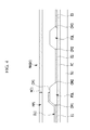
- FIG. 1 is a diagram illustrating a partial plane of an organic light emitting diode display according to a first embodiment.
- FIG. 1 mainly illustrates a first electrode, a pixel defining layer, and an organic emission layer.
- FIG. 2 is a cross-sectional view taken along line ⁇ - ⁇ of FIG. 1 .
- an organic light emitting diode display includes a substrate SU, a circuit part PC, a first electrode E1, a second electrode E2, a third electrode E3, a pixel defining layer PDL, a first organic emission layer OL1, a second organic emission layer OL2, a third organic emission layer OL3, and a common electrode CE.
- the substrate SU is formed by an insulating substrate made of glass, quartz, ceramics, metal, plastic, and the like. Further, in the case where the substrate SU is made of plastic, the organic light emitting diode display may have a flexible characteristic, and a stretchable or rollable characteristic.
- the circuit part PC is positioned on the substrate SU, and may include wires including one or more scan lines, data lines, driving power lines, common power lines, and the like, and a pixel circuit such as two or more thin film transistors (TFT) connected to the wires to correspond to one pixel and one or more capacitors, and the like.
- the circuit part PC may be formed to have various known structures.
- the first electrode E1 is positioned on the circuit part PC, and connected with the thin film transistor (TFT) of the circuit part PC.
- a central area of the first electrode E1 is positioned at a first vertex P1 of a virtual triangle VT.
- the virtual triangle VT is an isosceles triangle in which central areas of the first electrode E1, the second electrode E2, and the third electrode E3 which are adjacent to each other are connected to each other.
- a length of a first side V1 connecting the first vertex P1 and the third vertex P3 of the virtual triangle VT is the same as a length of a second side V2 connecting the second vertex P2 and the third vertex P3.
- the first electrode E1 may have various polygonal shapes, and the central area of the first electrode E1 is opened by a first opening OM1 of the pixel defining layer PDL.
- the second electrode E2 is positioned on the circuit part PC, and spaced apart from the first electrode E1.
- the second electrode E2 is connected with the thin film transistor (TFT) of the circuit part PC.
- a central area of the second electrode E2 is positioned at the second vertex P2 of the virtual triangle VT.
- the second electrode E2 may have various polygonal shapes, and the central area of the second electrode E2 is opened by a second opening OM2 of the pixel defining layer PDL.
- the third electrode E3 is spaced apart from the first electrode E1 and the second electrode E2 and positioned on the circuit part PC.
- the third electrode E3 is connected with the thin film transistor (TFT) of the circuit part PC.
- a central area of the third electrode E3 is positioned at the third vertex P3 of the virtual triangle VT.
- the third electrode E3 may have various polygonal shapes, and the central area of the third electrode E3 is opened by a third opening OM3 of the pixel defining layer PDL.
- the first electrode E1 and the second electrode E2 are disposed on a virtual square with the third electrode E3 as the center, and the first electrode E1 and the second electrode E2 surround the third electrode E3 with the third electrode E3 as the center.
- Each of the first electrode E1, the second electrode E2, and the third electrode E3 may be an anode functioning as a hole injection electrode or a cathode.
- the first electrode E1, the second electrode E2, and the third electrode E3 may be formed by light transmitting electrodes or light reflecting electrodes.
- the pixel defining layer PDL is positioned on the first electrode E1, the second electrode E2, and the third electrode E3, respectively, and covers edges of the first electrode E1, the second electrode E2, and the third electrode E3.
- the pixel defining layer PDL includes the first opening OM1, the second opening OM2, and the third opening OM3.
- the first opening OM1 opens the first electrode E1 and has a first polygonal shape which is a quadrangle.
- the first opening OM1 is spaced apart from the third opening OM3 and the second opening OM2, and a central point thereof is positioned at the first vertex P1 of the virtual triangle VT.
- the first opening OM1 has a larger area than the adjacent third opening OM3 and has a smaller area than the adjacent second opening OM2.
- the first opening OM1 has a quadrangular shape among the polygonal shapes, but is not limited thereto and may have polygonal shapes such as a triangle, a pentagon, a hexagon, a heptagon, and an octagon.
- a plurality of first openings OM1 is included, and the plurality of first openings OM1 has the same quadrangular shape.
- the plurality of first openings OM1 is spaced apart from each other with the third opening OM3 therebetween.
- the first organic emission layer OL1 emitting red light is positioned on the first electrode E1 opened by the first opening OM1.
- an organic emission layer emitting various colored light such as blue, green, or white may be positioned on the first electrode E1 opened by the first opening OM1.
- the second opening OM2 opens the second electrode E2 and has a second polygonal shape which is a hexagon.
- the second opening OM2 is spaced apart from the first opening OM1 and the third opening OM3, respectively, and a central point thereof is positioned at the second vertex P2 of the virtual triangle VT.
- the second opening OM2 has a larger area than the adjacent third opening OM3 and first opening OM1, respectively.
- the second opening OM2 has a hexagonal shape among the polygonal shapes, but is not limited thereto and may have polygonal shapes such as a triangle, a quadrangle, a pentagon, a heptagon, and an octagon.
- a plurality of second openings OM2, and the plurality of second openings OM2 has the same hexagonal shape.
- the plurality of second openings OM2 is spaced apart from each other with the third opening OM3 therebetween.
- the second organic emission layer OL2 emitting blue light is positioned on the second electrode E2 opened by the second opening OM2.
- an organic emission layer emitting various colored light such as red, green, or white may be positioned on the second electrode E2 opened by the second opening OM2.
- the third opening OM3 opens the third electrode E3 and has a third polygonal shape which is an octagon.
- the third opening OM3 is spaced apart from the first opening OM1 and the second opening OM2, respectively, and a central point thereof is positioned at the third vertex P3 of the virtual triangle VT.
- the third opening OM3 has a smaller area than the adjacent second opening OM2 and first opening OM1, respectively.
- the third opening OM3 has an octagonal shape among the polygonal shapes, but is not limited there to and may have polygonal shapes such as a triangle, a quadrangle, a pentagon, a hexagon, and a heptagon.
- a plurality of third openings OM3 is included, and adjacent third openings OM3 among the plurality of third openings OM3 have octagonal shapes which are symmetrical to each other. Meanwhile, the plurality of third openings OM3 may have the same octagonal shape.
- the third organic emission layer OL3 emitting green light is positioned on the third electrode E3 opened by the third opening OM3.
- an organic emission layer emitting various colored light such as blue, red, or white may be positioned on the third electrode E3 opened by the third opening OM3.
- center of the third opening OM3 is positioned at the central point of the virtual square, and centers of the first opening OM1 and the second opening OM2 surrounding the third opening OM3 along the virtual square may be positioned at adjacent vertexes of the virtual square, respectively.
- the first organic emission layer OL1 is positioned on the pixel defining layer PDL through the first electrode E1 corresponding to the first opening OM1.
- the first organic emission layer OL1 includes a first chamfer CM1 adjacent to a corner of the first opening OM1 which is a quadrangle.
- a 'chamfer' refers to a truncated corner portion.
- Such truncated corner portions may also be in a form of a convex portion as described in other embodiments.
- the first chamfer CM1 may be an edge of the first organic emission layer OL1 that intersects a straight line crossing the central point of the first opening OM1 and a vertex, for example, the corner, of the first opening OM1, wherein the vertex or the corner of the first opening OM1 is disposed between the first chamfer CM1 and the central point of the first opening OM1.
- the entire edge of the first organic emission layer OL1 has a hexadecagonal shape, and includes four first chamfers CM1 and four first connection portions CO1 connecting ends of the first chamfers CM1.
- Each of the four first connection portions CO1 is curved twice and extended to connect the adjacent first chamfers CM1.
- the first connection portions CO1 are curved once or three times or more and extended or extended in a straight line to connect the adjacent first chamfers CM1.
- the entire edge of the first organic emission layer OL1 includes four first chamfers CM1 and four first connection portions CO1, and as a result, a distance L1 between one edge of the first opening OM1 disposed on a first virtual straight line VL1 traversing the first opening OM1 and one edge of the first organic emission layer OL1 is different from a second distance L2 between the other edge of the first opening OM1 disposed on a second virtual straight line VL2 which is parallel to the first straight line VL1 to traverse the first opening OM1 and the other edge of the first organic emission layer OL1.
- the same first connection portion CO1 has at least two points that have different distances from a same edge, which is disposed between the same first connection portion CO1 and a central point of the first opening OM1, of the first opening OM1. More specifically, the second distance L2 close to the first chamfer CM1 adjacent to the corner of the first opening OM1 is longer than the first distance L1.
- the first organic emission layer OL1 includes an organic material emitting red light, and a portion which is positioned at the first opening OM1 and contacts the first electrode E1 emits red light. That is, the first organic emission layer OL1 has a quadrangular shape which is the first polygonal shape of the first opening OM1 and emits the red light.
- the first organic emission layer OL1 may include an organic material emitting blue, green, or white light, and in this case, the portion which is positioned at the first opening OM1 and contacts the first electrode E1 emits blue, green, or white light.
- the second organic emission layer OL2 is positioned on the pixel defining layer PDL through the second electrode E2 corresponding to the second opening OM2.
- the second organic emission layer OL2 includes a second chamfer CM2 adjacent to a corner of the second opening OM2 which is a hexagon.
- the entire edge of the second organic emission layer OL2 has a hexadecagonal shape, and includes four second chamfers CM2 and four second connection portions CO2 connecting ends of the second chamfers CM2.
- Each of the four second connection portions CO2 is curved twice and extended to connect the adjacent second chamfers CM2.
- the second connection portions CO2 are curved once or three times or more and extended or extended in a straight line to connect the adjacent second chamfers CM2.
- the second chamfer CM2 of the second organic emission layer OL2 is overlapped with the first chamfer CM1 of the first organic emission layer OL1 at a top portion of the pixel defining layer PDL. Even though the second chamfer CM2 of the second organic emission layer OL2 is overlapped with the first chamfer CM1 of the first organic emission layer OL1, since the first electrode E1 or the second electrode E2 is not positioned at the top portion of the pixel defining layer PDL, the first chamfer CM1 of the first organic emission layer OL1 and the second chamfer CM2 of the second organic emission layer OL2 which are the overlapped portions do not emit light.
- the second organic emission layer OL2 includes an organic material emitting blue light, and a portion which is positioned at the second opening OM2 and contacts the second electrode E2 emits blue light. That is, the second organic emission layer OL2 has a hexagonal shape which is the second polygonal shape of the second opening OM2 and emits the blue light.
- the second organic emission layer OL2 may include an organic material emitting red, green, or white light, and in this case, the portion which is positioned at the second opening OM2 and contacts the second electrode E2 emits red, green, or white light.
- the third organic emission layer OL3 is positioned on the pixel defining layer PDL through the third electrode E3 corresponding to the third opening OM3.
- the entire edge of the third organic emission layer OL3 has an octagonal shape having a larger area than the third opening OM3.
- the partial edge spaced apart from the first chamfer CM1 and the second chamfer CM2 among the entire edges of the third organic emission layer OL3 is overlapped with the edges of the first organic emission layer OL1 and the second organic emission layer OL2 at a top portion of the pixel defining layer PDL, respectively.
- the partial edge of the third organic emission layer OL3 is overlapped with the edges of the first organic emission layer OL1 and the second organic emission layer OL2, respectively, since the first electrode E1, the second electrode E2, or the third electrode E3 is not positioned at the top portion of the pixel defining layer PDL, the partial edges of the first organic emission layer OL1, the second organic emission layer OL2, and the third organic emission layer OL3 which are the overlapped portions do not emit light.
- the third organic emission layer OL3 includes an organic material emitting green light, and a portion which is positioned at the third opening OM3 and contacts the third electrode E3 emits green light. That is, the third organic emission layer OL3 has an octagonal shape which is the third polygonal shape of the third opening OM3 and emits the green light.
- the third organic emission layer OL3 may include an organic material emitting red, blue, or white light, and in this case, the portion which is positioned at the third opening OM3 and contacts the third electrode E3 emits red, blue, or white light.
- the common electrodes CE are positioned on the first organic emission layer OL1, the second organic emission layer OL2, and the third organic emission layer OL3 all over the surface of the substrate SU, and each of the common electrodes CE may be a cathode functioning as an electron injection electrode or an anode.
- the common electrode CE may be formed as a light transmitting electrode or a light reflecting electrode.
- the organic light emitting diode display according to the first embodiment is implemented at high resolution in a limited display area, and as a result, distances between the corners of the first opening OM1, the second opening OM2, and the third opening OM3 which are adjacent to each other are decreased and simultaneously, the first organic emission layer OL1 is formed to have a larger area than the first opening OM1.
- the first organic emission layer OL1 includes the first chamfer CM1 adjacent to the corner of the first opening OM1, and as a result, when the first organic emission layer OL1 is deposited, the first chamfer CM1 which is an outermost edge of the first organic emission layer OL1 is prevented from intruding into the second opening OM2 or the third opening OM3. That is, the organic light emitting diode display, which prevents colors of light emitted from the first opening OM1, the second opening OM2, and the third opening OM3 from being mixed, is provided.
- the organic light emitting diode display according to the first embodiment is implemented at high resolution in a limited display area, and as a result, distances between the corners of the first opening OM1, the second opening OM2, and the third opening OM3 which are adjacent to each other are decreased and simultaneously, the second organic emission layer OL2 is formed to have a larger area than the second opening OM2.
- the second organic emission layer OL2 includes the second chamfer CM2 adjacent to the corner of the second opening OM2, and as a result, when the second organic emission layer OL2 is deposited, the second chamfer CM2 which is an outermost edge of the second organic emission layer OL2 is prevented from intruding into the first opening OM1 or the third opening OM3. That is, the organic light emitting diode display, which prevents colors of light emitted from the first opening OM1, the second opening OM2, and the third opening OM3 from being mixed, is provided.
- the mask unit includes a first mask, a second mask, and a third mask used when the first organic emission layer, the second organic emission layer, and the third organic emission layer are manufactured.
- FIG. 3 is a diagram illustrating a partial plane of a first mask of a mask unit according to a second embodiment.
- FIG. 4 is a diagram for describing formation of a first organic emission layer using the first mask illustrated in FIG. 3 .
- a first mask MASK1 of the mask unit according to the second embodiment is used when depositing the first organic emission layer OL1 and includes a first mask pattern portion MP1.
- the first mask MASK1 is disposed on the pixel defining layer PDL during a depositing process for forming the first organic emission layer OL1.
- the first mask pattern portion MP1 is positioned on the first electrode E1, disposed on the pixel defining layer PDL including the first opening OM1 having a first polygonal shape opening the first electrode E1, and used when the first organic emission layer OL1 is formed.
- the first mask pattern portion MP1 has a dotted shape, and is through-formed to correspond to the pixel defining layer PDL through the first electrode E1 corresponding to the first opening OM1.
- the first mask pattern portion MP1 includes a first mask chamfer MC1 corresponding to the corner of the first opening OM1.
- the entire edge of the first mask pattern portion MP1 has a hexadecagonal shape corresponding to the entire shape of the first organic emission layer OL1, and includes four first mask chamfers MC1 which are spaced apart from each other and four first mask connection portions MO1 connecting ends of the first mask chamfers MC1.
- Each of the four first mask connection portions MO1 is curved twice and extended to connect the adjacent first mask chamfers MC1.
- the first mask connection portions MO1 are curved once or three times or more and extended or extended in a straight line to connect the adjacent first mask chamfers MC1.
- the first organic emission layer OL1 is formed on the first electrode E1 through the first mask pattern portion MP1.
- FIG. 5 is a diagram illustrating a partial plane of a second mask of the mask unit according to the second embodiment.
- FIG. 6 is a diagram for describing formation of a second organic emission layer using the second mask illustrated in FIG. 5 .
- a second mask MASK2 of the mask unit according to the second embodiment is used when depositing the second organic emission layer OL2 and includes a second mask pattern portion MP2.
- the second mask MASK2 is disposed on the pixel defining layer PDL during a depositing process for forming the second organic emission layer OL2.
- the second mask pattern portion MP2 is positioned on the second electrode E2, disposed on the pixel defining layer PDL including the second opening OM2 having a second polygonal shape opening the second electrode E2, and used when the second organic emission layer OL2 is formed.
- the second mask pattern portion MP2 has a dotted shape, and is through-formed to correspond to the pixel defining layer PDL through the second electrode E2 corresponding to the second opening OM2.
- the second mask pattern portion MP2 includes a second mask chamfer MC2 corresponding to the corner of the second opening OM2.
- the entire edge of the second mask pattern portion MP2 has a hexadecagonal shape corresponding to the entire shape of the second organic emission layer OL2, and includes four second mask chamfers MC2 which are spaced apart from each other and four second mask connection portions M02 connecting ends of the second mask chamfers MC2.
- Each of the four second mask connection portions M02 is curved twice and extended to connect the adjacent second mask chamfers MC2.
- the second mask connection portions M02 are curved once or three times or more and extended or extended in a straight line to connect the adjacent second mask chamfers MC2.
- the second mask chamfer MC2 of the second mask pattern portion MP2 is overlapped with the first chamfer CM1 of the first organic emission layer OL1 formed on the pixel defining layer PDL through the first mask pattern portion MP1 of the first mask MASK1.
- the second organic emission layer OL2 is formed on the second electrode E2 through the second mask pattern portion MP2.
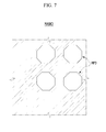
- FIG. 7 is a diagram illustrating a partial plane of a third mask of the mask unit according to the second embodiment.
- FIG. 8 is a diagram for describing formation of a third organic emission layer using the third mask illustrated in FIG. 7 .
- a third mask MASK3 of the mask unit according to the second embodiment is used when depositing the third organic emission layer OL3 and includes a third mask pattern portion MP3.
- the third mask MASK3 is disposed on the pixel defining layer PDL during a depositing process for forming the third organic emission layer OL3.
- the third mask pattern portion MP3 is positioned on the third electrode E3, disposed on the pixel defining layer PDL including the third opening OM3 having a third polygonal shape opening the third electrode E3, and used when the third organic emission layer OL3 is formed.
- the third mask pattern portion MP3 has a dotted shape, and is through-formed to correspond to the pixel defining layer PDL through the third electrode E3 corresponding to the third opening OM3.
- the third mask pattern portion MP3 is formed in a shape corresponding to the third opening OM3.
- the entire edge of the third mask pattern portion MP3 has an octagonal shape to correspond to the entire shape of the third organic emission layer OL3.
- the third organic emission layer OL3 is formed on the third electrode E3 through the third mask pattern portion MP3.
- the first mask pattern portion MP1, the second mask pattern portion MP2, and the third mask pattern portion MP3 of the first mask MASK1, the second mask MASK2, and the third mask MASK3 are expanded up to the top portion of the pixel defining layer PDL through the first opening OM1, the second opening OM2, and the third opening OM3 to be largely formed, and as a result, the first mask pattern portion MP1, the second mask pattern portion MP2, and the third mask pattern portion MP3 may be easily formed at the first mask MASK1, the second mask MASK2, and the third mask MASK3, respectively. That is, the mask unit including the first mask MASK1, the second mask MASK2, and the third mask MASK3 of which manufacturing yield is improved is provided.
- the first mask pattern portion MP1 and the second mask pattern portion MP2 include the first mask chamfer MC1 corresponding to the corner of the first opening OM1 and the second mask chamfer MC2 corresponding to the corner of the second opening OM2 and as a result, when the first organic emission layer OL1 and the second organic emission layer OL2 are deposited through the first mask pattern portion MP1 and the second mask pattern portion MP2, the first chamfer CM1 which is an outermost edge of the first organic emission layer OL1 is prevented from intruding into the second opening OM2 or the third opening OM3 and simultaneously, the second chamfer CM2 which is an outermost edge of the second organic emission layer OL2 is prevented from intruding into the
- FIG. 9 is a diagram illustrating a partial plane of an organic light emitting diode display according to a third embodiment.
- the organic light emitting diode display according to the third embodiment may be an organic light emitting diode display which is manufactured by a process error generated when designing the organic light emitting diode display according to the first embodiment described above and manufacturing the designed organic light emitting diode display.
- an organic light emitting diode display includes a substrate, a circuit part, a first electrode E1, a second electrode E2, a third electrode E3, a pixel defining layer PDL, a first organic emission layer OL1, a second organic emission layer OL2, a third organic emission layer OL3, and a common electrode.
- the first electrode E1 is positioned on the circuit part and connected with a thin film transistor of the circuit part.
- a central area of the first electrode E1 is positioned at a first vertex P1 of a virtual triangle VT.
- the virtual triangle VT is an isosceles triangle in which central areas of the first electrode E1, the second electrode E2, and the third electrode E3 which are adjacent to each other are connected to each other.
- a length of a first side V1 connecting the first vertex P1 and a third vertex P3 of the virtual triangle VT is the same as a length of a second side V2 connecting the second vertex P2 and the third vertex P3.
- the first electrode E1 may have various polygonal shapes, and the central area of the first electrode E1 is opened by a first opening OM1 of the pixel defining layer PDL.
- the second electrode E2 is positioned on the circuit part, and spaced apart from the first electrode E1.
- the second electrode E2 is connected with a thin film transistor of the circuit part.
- a central area of the second electrode E2 is positioned at the second vertex P2 of the virtual triangle VT.
- the second electrode E2 may have various polygonal shapes, and the central area of the second electrode E2 is opened by a second opening OM2 of the pixel defining layer PDL.
- the third electrode E3 is spaced apart from the first electrode E1 and the second electrode E2 and positioned on the circuit part.
- the third electrode E3 is connected with the thin film transistor (TFT) of the circuit part PC.
- TFT thin film transistor
- a central area of the third electrode E3 is positioned at the third vertex P3 of the virtual triangle VT.
- the third electrode E3 may have various polygonal shapes, and the central area of the third electrode E3 is opened by a third opening OM3 of the pixel defining layer PDL.
- the first electrode E1 and the second electrode E2 are disposed on a virtual square with the third electrode E3 as the center, and the first electrode E1 and the second electrode E2 surround the third electrode E3 with the third electrode E3 as the center.
- Each of the first electrode E1, the second electrode E2, and the third electrode E3 may be an anode functioning as a hole injection electrode or a cathode.
- the first electrode E1, the second electrode E2, and the third electrode E3 may be formed by light transmitting electrodes or light reflecting electrodes.
- the pixel defining layer PDL is positioned on the first electrode E1, the second electrode E2, and the third electrode E3, respectively, and covers edges of the first electrode E1, the second electrode E2, and the third electrode E3.
- the pixel defining layer PDL includes the first opening OM1, the second opening OM2, and the third opening OM3.
- the first opening OM1 opens the first electrode E1 and has a first polygonal shape which is a quadrangle.
- the first opening OM1 is spaced apart from the third opening OM3 and the second opening OM2, respectively, and a central point thereof is positioned at the first vertex P1 of the virtual triangle VT.
- the first opening OM1 has a larger area than the adjacent third opening OM3 and has a smaller area than the adjacent second opening OM2.
- the first opening OM1 has a quadrangular shape among the polygonal shapes, but is not limited thereto and may have polygonal shapes such as a triangle, a pentagon, a hexagon, a heptagon, and an octagon.
- a plurality of first openings OM1 is included, and the plurality of first openings OM1 has the same quadrangular shape.
- the plurality of first openings OM1 is spaced apart from each other with the third opening OM3 therebetween.
- the first organic emission layer OL1 emitting red light is positioned on the first electrode E1 opened by the first opening OM1.
- an organic emission layer emitting various colored light such as blue, green, or white may be positioned on the first electrode E1 opened by the first opening OM1.
- the second opening OM2 opens the second electrode E2 and has a second polygonal shape which is a hexagon.
- the second opening OM2 is spaced apart from the first opening OM1 and the third opening OM3, respectively, and a central point thereof is positioned at the second vertex P2 of the virtual triangle VT.
- the second opening OM2 has a larger area than the adjacent third opening OM3 and the adjacent first opening OM1, respectively.
- the second opening OM2 has a hexagonal shape among the polygonal shapes, but is not limited thereto and may have polygonal shapes such as a triangle, a quadrangle, a pentagon, a heptagon, and an octagon.
- a plurality of second openings OM2 is included, and the plurality of second openings OM2 has the same hexagonal shape.
- the plurality of second openings OM2 is spaced apart from each other with the third opening OM3 therebetween.
- the second organic emission layer OL2 emitting blue light is positioned on the second electrode E2 opened by the second opening OM2.
- an organic emission layer emitting various colored light such as red, green, or white may be positioned on the second electrode E2 opened by the second opening OM2.
- the third opening OM3 opens the third electrode E3 and has a third polygonal shape which is an octagon.
- the third opening OM3 is spaced apart from the first opening OM1 and the second opening OM2, respectively, and a central point thereof is positioned at the third vertex P3 of the virtual triangle VT.
- the third opening OM3 has a smaller area than the adjacent second opening OM2 and first opening OM1, respectively.
- the third opening OM3 has an octagonal shape among the polygonal shapes, but is not limited thereto and may have polygonal shapes such as a triangle, a quadrangle, a pentagon, a hexagon, and a heptagon.
- a plurality of third openings OM3 is included, and adjacent third openings OM3 among the plurality of third openings OM3 have octagonal shapes which are symmetrical to each other. Meanwhile, the plurality of third openings OM3 may have the same octagonal shape.
- the third organic emission layer OL3 emitting green light is positioned on the third electrode E3 opened by the third opening OM3.
- an organic emission layer emitting various colored light such as blue, red, or white may be positioned on the third electrode E3 opened by the third opening OM3.
- center of the third opening OM3 is positioned at the central point of the virtual square, and centers of the first opening OM1 and the second opening OM2 surrounding the third opening OM3 along the virtual square may be positioned at adjacent vertexes of the virtual square, respectively.
- the first organic emission layer OL1 is positioned on the pixel defining layer PDL through the first electrode E1 corresponding to the first opening OM1.
- the first organic emission layer OL1 includes a first convex portion CON1 adjacent to a corner of the first opening OM1 which is a quadrangle.
- the first convex portion CON1 intersects a straight line crossing the central point of the first opening OM1 and a vertex, for example, the corner, of the first opening OM1, wherein the vertex or the corner of the first opening OM1 is disposed between the first convex portion CON1 and the central point of the first opening OM1.
- the entire edge of the first organic emission layer OL1 has a closed loop shape formed by curved lines, and is configured by four first convex portions CON1 which are connected to each other.
- a connection portion between the adjacent first convex portions CON1 is formed by a concave portion.
- the entire edge of the first organic emission layer OL1 includes the four first convex portions CON1, and as a result, a first distance L1 between one edge of the first opening OM1 disposed on a first virtual straight line VL1 traversing the first opening OM1 and one edge of the first organic emission layer OL1 is different from a second distance L2 between the other edge of the first opening OM1 disposed on a second virtual straight line VL2 which is parallel to the first straight line VL1 to traverse the first opening OM1 and the other edge of the first organic emission layer OL1. That is, the second distance L2 close to the first convex portion CON1 adjacent to the corner of the first opening OM1 is longer than the first distance L1.
- the first organic emission layer OL1 includes an organic material emitting red light, and a portion which is positioned at the first opening OM1 and contacts the first electrode E1 emits red light. That is, the first organic emission layer OL1 has a quadrangular shape which is the first polygonal shape of the first opening OM1 and emits the red light.
- the first organic emission layer OL1 may include an organic material emitting blue, green, or white light, and in this case, the portion which is positioned at the first opening OM1 and contacts the first electrode E1 emits blue, green, or white light.
- the second organic emission layer OL2 is positioned on the pixel defining layer PDL through the second electrode E2 corresponding to the second opening OM2.
- the second organic emission layer OL2 includes a second convex portion CON2 adjacent to a corner of the second opening OM2 which is a hexagon.
- the entire edge of the second organic emission layer OL2 has a closed loop shape formed by curved lines, and is configured by four second convex portions CON2 which are connected to each other.
- a connection portion between the adjacent second convex portions CON2 is formed by a concave portion.
- the second convex portion CON2 of the second organic emission layer OL2 is overlapped with the first convex portion CON1 of the first organic emission layer OL1 at a top portion of the pixel defining layer PDL.
- the second convex portion CON2 of the second organic emission layer OL2 is overlapped with the first convex portion CON1 of the first organic emission layer OL1
- the first electrode E1 or the second electrode E2 is not positioned at the top portion of the pixel defining layer PDL, the first convex portion CON1 of the first organic emission layer OL1 and the second convex portion CON2 of the second organic emission layer OL2 which are the overlapped portions do not emit light.
- the second organic emission layer OL2 includes an organic material emitting blue light, and a portion which is positioned at the second opening OM2 and contacts the second electrode E2 emits blue light. That is, the second organic emission layer OL2 has a hexagonal shape which is the second polygonal shape of the second opening OM2 and emits the blue light.
- the second organic emission layer OL2 may include an organic material emitting red, green, or white light, and in this case, the portion which is positioned at the second opening OM2 and contacts the second electrode E2 emits red, green, or white light.
- the third organic emission layer OL3 is positioned on the pixel defining layer PDL through the third electrode E3 corresponding to the third opening OM3.
- the entire edge of the third organic emission layer OL3 has a closed loop shape surrounding the third opening OM3 and is not overlapped with each edge of the first organic emission layer OL1 and the second organic emission layer OL2.
- the third organic emission layer OL3 includes an organic material emitting green light, and a portion which is positioned at the third opening OM3 and contacts the third electrode E3 emits green light. That is, the third organic emission layer OL3 has an octagonal shape which is the third polygonal shape of the third opening OM3 and emits the green light.
- the third organic emission layer OL3 may include an organic material emitting red, blue, or white light, and in this case, the portion which is positioned at the third opening OM3 and contacts the third electrode E3 emits red, blue, or white light.
- the opened first mask pattern portion, second mask pattern portion, and third mask pattern portion of the used first mask, second mask, and third mask may have the same shape as the first organic emission layer OL1, the second organic emission layer OL2, and the third organic emission layer OL3, respectively.
- the organic light emitting diode display according to the third embodiment is implemented at high resolution in a limited display area, and as a result, distances between the corners of the first opening OM1, the second opening OM2, and the third opening OM3 which are adjacent to each other are decreased and simultaneously, the first organic emission layer OL1 is formed to have a larger area than the first opening OM1.
- the first organic emission layer OL1 includes the first convex portion CON1 adjacent to the corner of the first opening OM1, and as a result, when the first organic emission layer OL1 is deposited, the first convex portion CON1 which is an outermost edge of the first organic emission layer OL1 is prevented from intruding into the second opening OM2 or the third opening OM3. That is, the organic light emitting diode display, which prevents colors of light emitted from the first opening OM1, the second opening OM2, the third opening OM3 from being mixed, is provided.
- the organic light emitting diode display according to the third embodiment is implemented at high resolution in a limited display area, and as a result, distances between the corners of the first opening OM1, the second opening OM2, and the third opening OM3 which are adjacent to each other are decreased and simultaneously, the second organic emission layer OL2 is formed to have a larger area than the second opening OM2.
- the second organic emission layer OL2 includes the second convex portion CON2 adjacent to the corner of the second opening OM2, and as a result, when the second organic emission layer OL2 is deposited, the second convex portion CON2 which is an outermost edge of the second organic emission layer OL2 is prevented from intruding into the first opening OM1 or the third opening OM3. That is, the organic light emitting diode display, which prevents colors of light emitted from the first opening OM1, the second opening OM2, and the third opening OM3 from being mixed, is provided.
- the first organic emission layer OL1 covers the entire first opening OM1 and also covers a portion of the pixel defining layer PDL that forms the first opening OM1.
- an area of the first organic emission layer OL1 is greater than an area of the first opening OM1.
- an outer shape of the first organic emission layer OL1 is geometrically dissimilar to the first polygon formed by the first opening OM1.
- the outer shape of the first organic emission layer OL1 of the first embodiment shown in FIG. 1 has more edges than the first opening OM1 due to the first chamfers CM1 and the curved first connection portions C01.
- the outer shape of the first organic emission layer OL1 of the third embodiment shown in FIG. 9 has the convex portions CON1 and the concave portions connecting the convex portions CON1.
- the first opening OM1 has four straight edges.
- an area of the second organic emission layer OL2 is greater than an area of the second opening OM2, but on the other hand, an outer shape of the second organic emission layer OL2 is geometrically dissimilar to the second polygon formed by the second opening OM2.
- an organic light emitting diode display preventing colors of light emitted by one pixel from being mixed, even though the organic light emitting diode display is implemented at high resolution in a limited display area.
Landscapes
- Engineering & Computer Science (AREA)
- Physics & Mathematics (AREA)
- Microelectronics & Electronic Packaging (AREA)
- Geometry (AREA)
- Optics & Photonics (AREA)
- General Physics & Mathematics (AREA)
- Theoretical Computer Science (AREA)
- Manufacturing & Machinery (AREA)
- Computer Hardware Design (AREA)
- Electroluminescent Light Sources (AREA)
- Devices For Indicating Variable Information By Combining Individual Elements (AREA)
Applications Claiming Priority (1)
| Application Number | Priority Date | Filing Date | Title |
|---|---|---|---|
| KR20130046362A KR101485166B1 (ko) | 2013-04-25 | 2013-04-25 | 유기 발광 표시 장치 및 마스크 유닛 |
Publications (3)
| Publication Number | Publication Date |
|---|---|
| EP2797115A2 true EP2797115A2 (fr) | 2014-10-29 |
| EP2797115A3 EP2797115A3 (fr) | 2015-01-28 |
| EP2797115B1 EP2797115B1 (fr) | 2021-03-03 |
Family
ID=50543494
Family Applications (1)
| Application Number | Title | Priority Date | Filing Date |
|---|---|---|---|
| EP14165873.2A Active EP2797115B1 (fr) | 2013-04-25 | 2014-04-24 | Affichage à diode électroluminescente organique et son procédé de fabrication |
Country Status (5)
| Country | Link |
|---|---|
| US (5) | US9484391B2 (fr) |
| EP (1) | EP2797115B1 (fr) |
| KR (1) | KR101485166B1 (fr) |
| CN (2) | CN109599418B (fr) |
| TW (6) | TWI624935B (fr) |
Cited By (4)
| Publication number | Priority date | Publication date | Assignee | Title |
|---|---|---|---|---|
| CN112002726A (zh) * | 2019-05-27 | 2020-11-27 | 三星显示有限公司 | 显示设备和制造该显示设备的方法 |
| EP3686933A4 (fr) * | 2017-09-18 | 2021-08-18 | BOE Technology Group Co., Ltd. | Substrat d'affichage, dispositif d'affichage et procédé de fabrication du substrat de réseau |
| EP3748680A4 (fr) * | 2018-02-01 | 2021-10-20 | Wuhan China Star Optoelectronics Semiconductor Display Technology Co., Ltd. | Structure d'agencement de pixel |
| CN113540387A (zh) * | 2021-07-15 | 2021-10-22 | 昆山梦显电子科技有限公司 | 一种微显示器及其制作方法 |
Families Citing this family (57)
| Publication number | Priority date | Publication date | Assignee | Title |
|---|---|---|---|---|
| CN104576695B (zh) * | 2014-12-22 | 2017-08-25 | 信利(惠州)智能显示有限公司 | Oled像素排列结构及显示装置 |
| KR102471237B1 (ko) * | 2015-01-21 | 2022-11-28 | 삼성디스플레이 주식회사 | 폴더블 표시장치 |
| KR102378421B1 (ko) * | 2015-03-31 | 2022-03-25 | 삼성디스플레이 주식회사 | 증착용 마스크 세트 및 이를 이용한 표시 패널의 제조 방법 |
| KR102547213B1 (ko) * | 2015-06-15 | 2023-06-26 | 삼성디스플레이 주식회사 | 유기 발광 표시 장치 및 유기 발광 표시 장치의 제조 방법 |
| WO2017169961A1 (fr) * | 2016-03-31 | 2017-10-05 | ソニー株式会社 | Dispositif d'affichage et dispositif électronique |
| KR102679664B1 (ko) * | 2016-09-02 | 2024-06-28 | 삼성디스플레이 주식회사 | 유기 발광 표시 장치 |
| KR102825728B1 (ko) * | 2016-11-30 | 2025-06-26 | 엘지디스플레이 주식회사 | 유기 발광 다이오드 표시 장치 |
| CN108155205B (zh) * | 2016-12-02 | 2020-09-11 | 信利(惠州)智能显示有限公司 | 一种amoled显示器 |
| KR102792403B1 (ko) | 2017-01-12 | 2025-04-07 | 삼성디스플레이 주식회사 | 유기발광 표시장치 |
| KR102838375B1 (ko) * | 2017-01-24 | 2025-07-25 | 삼성디스플레이 주식회사 | 전기 도금 마스크, 이를 이용하여 제작된 유기발광 표시장치 및 이의 제작방법 |
| TWI658583B (zh) * | 2017-06-14 | 2019-05-01 | 友達光電股份有限公司 | 畫素陣列及其製造方法 |
| CN111149055A (zh) * | 2017-09-29 | 2020-05-12 | 夏普株式会社 | 光掩膜、显示装置以及显示装置的制造方法 |
| JP6978739B2 (ja) * | 2017-10-27 | 2021-12-08 | Tianma Japan株式会社 | Oled表示装置、マスク及びoled表示装置の製造方法 |
| CN109994509B (zh) | 2018-01-02 | 2025-01-03 | 京东方科技集团股份有限公司 | 一种像素排布结构及相关装置 |
| CN108258018A (zh) * | 2018-01-10 | 2018-07-06 | 上海天马有机发光显示技术有限公司 | 一种有机发光显示面板及其显示装置 |
| CN110137211A (zh) * | 2018-02-09 | 2019-08-16 | 京东方科技集团股份有限公司 | 一种像素排布结构、高精度金属掩模板及显示装置 |
| KR102587116B1 (ko) * | 2018-05-31 | 2023-10-10 | 삼성디스플레이 주식회사 | 표시 장치 |
| KR102622792B1 (ko) * | 2018-08-30 | 2024-01-08 | 엘지디스플레이 주식회사 | 발광 표시 장치 |
| CN109449178B (zh) * | 2018-10-15 | 2020-09-22 | Oppo广东移动通信有限公司 | 显示屏、显示装置及电子设备 |
| CN120187240A (zh) * | 2018-11-30 | 2025-06-20 | 京东方科技集团股份有限公司 | 像素结构和精细金属掩模板组 |
| KR102582392B1 (ko) * | 2018-12-10 | 2023-09-26 | 삼성디스플레이 주식회사 | 표시 장치 및 표시 장치 제조 방법 |
| KR102731596B1 (ko) | 2018-12-24 | 2024-11-22 | 삼성디스플레이 주식회사 | 표시 장치 및 그의 리페어 방법 |
| CN109728044B (zh) * | 2018-12-29 | 2021-07-30 | 武汉天马微电子有限公司 | 有机发光显示面板和显示装置 |
| KR102778472B1 (ko) * | 2019-02-08 | 2025-03-12 | 삼성디스플레이 주식회사 | 표시 장치 및 그 제조방법 |
| US20220190069A1 (en) * | 2019-03-27 | 2022-06-16 | Sharp Kabushiki Kaisha | Display device and deposition mask |
| CN112313801B (zh) * | 2019-05-14 | 2024-02-09 | 京东方科技集团股份有限公司 | 阵列基板及其制作方法、显示装置 |
| CN111969114B (zh) * | 2019-05-20 | 2022-04-12 | 京东方科技集团股份有限公司 | 显示面板、制造显示面板的方法和掩模板 |
| KR20200136551A (ko) * | 2019-05-27 | 2020-12-08 | 삼성디스플레이 주식회사 | 표시 장치 |
| CN110578112B (zh) * | 2019-08-09 | 2020-09-01 | 武汉华星光电半导体显示技术有限公司 | 一种掩膜版和像素结构 |
| JP7421284B2 (ja) * | 2019-08-09 | 2024-01-24 | JDI Design and Development 合同会社 | 表示パネル、および、表示パネルの製造方法 |
| CN112750863A (zh) * | 2019-10-31 | 2021-05-04 | 京东方科技集团股份有限公司 | 显示背板、掩膜版组件和显示装置 |
| KR102708648B1 (ko) * | 2019-11-07 | 2024-09-23 | 삼성디스플레이 주식회사 | 표시 장치 |
| US11903300B2 (en) * | 2019-11-18 | 2024-02-13 | Universal Display Corporation | Pixel configurations for high resolution OVJP printed OLED displays |
| KR102761517B1 (ko) * | 2019-11-26 | 2025-02-04 | 삼성디스플레이 주식회사 | 증막 마스크, 이를 이용한 디스플레이 장치의 제조 방법 및 디스플레이 장치 |
| KR102698236B1 (ko) * | 2019-12-16 | 2024-08-23 | 삼성디스플레이 주식회사 | 표시 장치 |
| KR102741307B1 (ko) * | 2019-12-30 | 2024-12-10 | 엘지디스플레이 주식회사 | 표시장치 |
| KR102916745B1 (ko) * | 2020-02-25 | 2026-01-22 | 삼성디스플레이 주식회사 | 표시 장치 |
| CN111599942B (zh) * | 2020-05-27 | 2022-12-27 | 京东方科技集团股份有限公司 | 阵列基板、显示面板及显示装置 |
| CN115996612A (zh) * | 2020-09-01 | 2023-04-21 | 京东方科技集团股份有限公司 | 显示面板以及显示装置 |
| MX2021016051A (es) | 2020-09-10 | 2022-04-07 | Boe Technology Group Co Ltd | Serie de pixeles y dispositivo de pantalla. |
| US12302730B2 (en) | 2020-09-29 | 2025-05-13 | Chengdu Boe Optoelectronics Technology Co., Ltd. | Pixel array and display device |
| CN114420722B (zh) | 2020-09-10 | 2026-03-06 | 京东方科技集团股份有限公司 | 显示基板及显示装置 |
| US11983040B2 (en) | 2020-10-15 | 2024-05-14 | Dell Products L.P. | Multi-axis edge bended display for infinity portable information handling system |
| KR20220064479A (ko) | 2020-11-11 | 2022-05-19 | 삼성디스플레이 주식회사 | 디스플레이 패널 및 이를 구비하는 디스플레이 장치 |
| CN115485848A (zh) * | 2020-11-30 | 2022-12-16 | 京东方科技集团股份有限公司 | 显示基板、显示装置及高精度金属掩模板 |
| KR20220091699A (ko) * | 2020-12-23 | 2022-07-01 | 삼성디스플레이 주식회사 | 마스크, 마스크 어셈블리 및 표시 패널 제조 방법 |
| CN112992997B (zh) * | 2021-02-09 | 2024-04-19 | 京东方科技集团股份有限公司 | 一种像素结构、显示基板、显示装置及显示方法 |
| KR102864436B1 (ko) | 2021-02-15 | 2025-09-25 | 삼성디스플레이 주식회사 | 표시 장치 |
| CN113053973B (zh) * | 2021-03-11 | 2023-04-07 | 云南创视界光电科技有限公司 | 显示基板、彩膜基板、显示面板及显示装置 |
| CN113130609B (zh) * | 2021-04-09 | 2025-01-17 | 京东方科技集团股份有限公司 | 显示面板、显示装置和掩模板 |
| CN115480727A (zh) * | 2021-05-31 | 2022-12-16 | 西安诺瓦星云科技股份有限公司 | 显示屏的显示方法、装置、存储介质和存储器 |
| CN120379471A (zh) * | 2021-06-25 | 2025-07-25 | 京东方科技集团股份有限公司 | 显示基板以及显示装置 |
| JP2023117639A (ja) * | 2022-02-14 | 2023-08-24 | 株式会社ジャパンディスプレイ | 表示装置 |
| US12495709B2 (en) | 2022-04-12 | 2025-12-09 | Samsung Display Co., Ltd. | Light emitting display device including light blocking member having an opening and manufacturing method thereof |
| CN115117134B (zh) * | 2022-06-28 | 2025-02-25 | 武汉天马微电子有限公司 | 显示面板及显示装置 |
| CN118434226A (zh) * | 2024-05-15 | 2024-08-02 | 京东方科技集团股份有限公司 | 显示基板、显示装置和掩膜板 |
| CN120981125B (zh) * | 2025-10-15 | 2026-01-02 | 武汉华星光电技术有限公司 | 显示面板 |
Family Cites Families (39)
| Publication number | Priority date | Publication date | Assignee | Title |
|---|---|---|---|---|
| US77189A (en) * | 1868-04-28 | heath | ||
| TW461228B (en) * | 2000-04-26 | 2001-10-21 | Ritdisplay Corp | Method to manufacture the non-photosensitive polyimide pixel definition layer of organic electro-luminescent display panel |
| US7110012B2 (en) * | 2000-06-12 | 2006-09-19 | Sharp Laboratories Of America, Inc. | System for improving display resolution |
| JP3620490B2 (ja) * | 2000-11-22 | 2005-02-16 | ソニー株式会社 | アクティブマトリクス型表示装置 |
| JP2002320235A (ja) * | 2001-04-19 | 2002-10-31 | Fujitsu Ltd | 空間解像度の低下を抑えて縮小画像信号を生成するcmosイメージセンサ |
| US7583279B2 (en) * | 2004-04-09 | 2009-09-01 | Samsung Electronics Co., Ltd. | Subpixel layouts and arrangements for high brightness displays |
| JP4287820B2 (ja) * | 2003-02-13 | 2009-07-01 | 富士フイルム株式会社 | 表示装置、及びその製造方法 |
| US7091941B2 (en) * | 2003-04-11 | 2006-08-15 | Eastman Kodak Company | Color OLED display with improved power efficiency |
| JP2005005227A (ja) * | 2003-06-16 | 2005-01-06 | Hitachi Displays Ltd | 有機el発光表示装置 |
| US7407252B2 (en) * | 2004-07-01 | 2008-08-05 | Applied Materials, Inc. | Area based optical proximity correction in raster scan printing |
| KR100635570B1 (ko) * | 2004-10-19 | 2006-10-17 | 삼성에스디아이 주식회사 | 유기전계발광표시장치의 제조방법 |
| JP5177957B2 (ja) | 2005-03-31 | 2013-04-10 | 株式会社半導体エネルギー研究所 | 表示装置、およびそれを用いた電子機器 |
| US8866707B2 (en) * | 2005-03-31 | 2014-10-21 | Semiconductor Energy Laboratory Co., Ltd. | Display device, and apparatus using the display device having a polygonal pixel electrode |
| KR101085449B1 (ko) * | 2005-04-12 | 2011-11-21 | 삼성전자주식회사 | 표시장치 |
| JP2007265696A (ja) * | 2006-03-27 | 2007-10-11 | Seiko Epson Corp | 発光装置の製造方法、発光装置および電子機器 |
| TWI361637B (en) * | 2007-09-20 | 2012-04-01 | Chi Mei El Corp | Organic light emitting panel and compound organic light emitting device |
| US20120138904A1 (en) * | 2007-09-21 | 2012-06-07 | Takahisa Shimizu | Organic electroluminescence display and production method thereof |
| KR101388582B1 (ko) * | 2007-10-26 | 2014-04-23 | 삼성디스플레이 주식회사 | 전기 영동 표시 장치 |
| US8330352B2 (en) * | 2007-11-13 | 2012-12-11 | Samsung Display Co., Ltd. | Organic light emitting diode display and method for manufacturing the same |
| JP4650495B2 (ja) * | 2008-02-05 | 2011-03-16 | セイコーエプソン株式会社 | 発光装置及び電子機器 |
| KR100953539B1 (ko) | 2008-06-11 | 2010-04-21 | 삼성모바일디스플레이주식회사 | 유기 발광 디스플레이 장치 |
| KR101499234B1 (ko) | 2008-06-27 | 2015-03-05 | 삼성디스플레이 주식회사 | 유기 발광 표시 장치, 그 제조 방법 및 이에 사용되는섀도우 마스크 |
| JP2010095744A (ja) * | 2008-10-15 | 2010-04-30 | Seiko Epson Corp | 蒸着マスク、蒸着マスクの製造方法、電気光学装置の製造方法および電子機器 |
| JP2010129345A (ja) * | 2008-11-27 | 2010-06-10 | Sumitomo Chemical Co Ltd | 有機エレクトロルミネッセンス素子の製造方法 |
| KR20120022967A (ko) | 2009-06-26 | 2012-03-12 | 세키스이가가쿠 고교가부시키가이샤 | 필름의 표면 처리 방법 및 장치, 및 편광판의 제조 방법 |
| KR101546552B1 (ko) * | 2009-11-11 | 2015-08-21 | 가부시키가이샤 제이올레드 | 유기 el 소자 및 그 제조 방법 |
| KR101084245B1 (ko) * | 2010-01-04 | 2011-11-16 | 삼성모바일디스플레이주식회사 | 표시 장치 |
| KR101189025B1 (ko) * | 2010-05-31 | 2012-10-08 | 삼성디스플레이 주식회사 | 유기전계발광 표시장치의 화소배열구조 |
| DE102011053000B4 (de) * | 2010-08-27 | 2017-08-17 | Lg Display Co., Ltd. | Organische elektrolumineszente Vorrichtung |
| KR101257734B1 (ko) * | 2010-09-08 | 2013-04-24 | 엘지디스플레이 주식회사 | 유기전계발광 표시장치 |
| KR101739384B1 (ko) | 2010-12-24 | 2017-05-25 | 엘지디스플레이 주식회사 | 화이트 유기발광다이오드 표시소자 및 그 제조방법 |
| KR101734920B1 (ko) | 2010-12-27 | 2017-05-12 | 엘지디스플레이 주식회사 | 유기전계발광소자 및 그 제조방법 |
| GB201105582D0 (en) * | 2011-04-01 | 2011-05-18 | Cambridge Display Tech Ltd | Organic light-emitting device and method |
| KR101845332B1 (ko) * | 2011-06-13 | 2018-05-21 | 삼성디스플레이 주식회사 | 유기 발광 표시 장치 및 그 제조 방법 |
| KR101328979B1 (ko) | 2011-06-30 | 2013-11-13 | 삼성디스플레이 주식회사 | 유기 발광 표시장치 |
| US8552420B2 (en) | 2011-08-09 | 2013-10-08 | Universal Display Corporation | OLED light panel with controlled brightness variation |
| KR101958434B1 (ko) | 2011-09-05 | 2019-03-15 | 삼성디스플레이 주식회사 | 유기 발광 표시 장치 |
| KR101615332B1 (ko) * | 2012-03-06 | 2016-04-26 | 삼성디스플레이 주식회사 | 유기 발광 표시 장치의 화소 배열 구조 |
| KR20140086315A (ko) * | 2012-12-28 | 2014-07-08 | 삼성디스플레이 주식회사 | 유기발광 표시패널 및 유기발광 표시패널의 제조방법 |
-
2013
- 2013-04-25 KR KR20130046362A patent/KR101485166B1/ko active Active
-
2014
- 2014-01-31 US US14/169,829 patent/US9484391B2/en active Active
- 2014-02-18 TW TW103105368A patent/TWI624935B/zh active
- 2014-02-18 TW TW111137218A patent/TWI854316B/zh active
- 2014-02-18 TW TW109115422A patent/TWI839515B/zh active
- 2014-02-18 TW TW107112002A patent/TWI696282B/zh active
- 2014-02-18 TW TW113115215A patent/TWI905729B/zh active
- 2014-02-18 TW TW114118036A patent/TW202535222A/zh unknown
- 2014-04-14 CN CN201811216252.2A patent/CN109599418B/zh active Active
- 2014-04-14 CN CN201410149137.3A patent/CN104124265B/zh active Active
- 2014-04-24 EP EP14165873.2A patent/EP2797115B1/fr active Active
-
2016
- 2016-10-03 US US15/284,210 patent/US11309356B2/en active Active
-
2022
- 2022-03-14 US US17/694,613 patent/US11997905B2/en active Active
-
2024
- 2024-03-28 US US18/620,692 patent/US20240244910A1/en active Pending
-
2025
- 2025-04-25 US US19/190,121 patent/US20250255134A1/en active Pending
Non-Patent Citations (1)
| Title |
|---|
| None |
Cited By (9)
| Publication number | Priority date | Publication date | Assignee | Title |
|---|---|---|---|---|
| EP3686933A4 (fr) * | 2017-09-18 | 2021-08-18 | BOE Technology Group Co., Ltd. | Substrat d'affichage, dispositif d'affichage et procédé de fabrication du substrat de réseau |
| US11233101B2 (en) | 2017-09-18 | 2022-01-25 | Boe Technology Group Co., Ltd. | Display substrate, display device, and manufacturing method of display substrate |
| EP3748680A4 (fr) * | 2018-02-01 | 2021-10-20 | Wuhan China Star Optoelectronics Semiconductor Display Technology Co., Ltd. | Structure d'agencement de pixel |
| CN112002726A (zh) * | 2019-05-27 | 2020-11-27 | 三星显示有限公司 | 显示设备和制造该显示设备的方法 |
| EP3745463A3 (fr) * | 2019-05-27 | 2021-01-06 | Samsung Display Co., Ltd. | Afficheur et son procédé de fabrication |
| US11469276B2 (en) | 2019-05-27 | 2022-10-11 | Samsung Display Co., Ltd. | OLED display apparatus including first and second pluralities of opposite electrodes having different shapes corresponding to a display area and sensor area |
| US11785829B2 (en) | 2019-05-27 | 2023-10-10 | Samsung Display Co., Ltd. | Display apparatus and method of manufacturing the same, the method including depositing different electrode portions by moving a mask |
| CN113540387A (zh) * | 2021-07-15 | 2021-10-22 | 昆山梦显电子科技有限公司 | 一种微显示器及其制作方法 |
| CN113540387B (zh) * | 2021-07-15 | 2024-05-24 | 昆山梦显电子科技有限公司 | 一种微显示器及其制作方法 |
Also Published As
| Publication number | Publication date |
|---|---|
| TW202303962A (zh) | 2023-01-16 |
| US20240244910A1 (en) | 2024-07-18 |
| TW202535222A (zh) | 2025-09-01 |
| EP2797115A3 (fr) | 2015-01-28 |
| CN104124265A (zh) | 2014-10-29 |
| CN109599418B (zh) | 2023-09-29 |
| KR101485166B1 (ko) | 2015-01-22 |
| TW202431967A (zh) | 2024-08-01 |
| US11997905B2 (en) | 2024-05-28 |
| TWI854316B (zh) | 2024-09-01 |
| US20220352260A1 (en) | 2022-11-03 |
| CN104124265B (zh) | 2018-11-13 |
| US11309356B2 (en) | 2022-04-19 |
| US9484391B2 (en) | 2016-11-01 |
| TWI696282B (zh) | 2020-06-11 |
| EP2797115B1 (fr) | 2021-03-03 |
| CN109599418A (zh) | 2019-04-09 |
| TW201830689A (zh) | 2018-08-16 |
| KR20140127690A (ko) | 2014-11-04 |
| TWI905729B (zh) | 2025-11-21 |
| US20250255134A1 (en) | 2025-08-07 |
| TW201442214A (zh) | 2014-11-01 |
| TW202034523A (zh) | 2020-09-16 |
| US20140319484A1 (en) | 2014-10-30 |
| TWI839515B (zh) | 2024-04-21 |
| US20170025483A1 (en) | 2017-01-26 |
| TWI624935B (zh) | 2018-05-21 |
Similar Documents
| Publication | Publication Date | Title |
|---|---|---|
| EP2797115A2 (fr) | Affichage à diode électroluminescente organique et unité de masque | |
| US12512050B2 (en) | Pixel arrangement structure for organic light emitting diode display | |
| TWI649870B (zh) | 有機發光二極體顯示器 | |
| US9508778B2 (en) | Organic light emitting diode display | |
| EP2637209B1 (fr) | Structure de disposition de pixels pour dispositif d'affichage électroluminescent organique | |
| KR102141166B1 (ko) | 유기 발광 표시 장치 및 마스크 유닛 | |
| KR101991431B1 (ko) | 유기 발광 표시 장치 및 마스크 유닛 | |
| KR20150044292A (ko) | 유기 발광 표시 장치 | |
| KR20160048744A (ko) | 유기 발광 표시 장치의 화소 배열 구조 | |
| KR102679664B1 (ko) | 유기 발광 표시 장치 | |
| US20260128007A1 (en) | Pixel arrangement structure for organic light emitting diode display |
Legal Events
| Date | Code | Title | Description |
|---|---|---|---|
| PUAI | Public reference made under article 153(3) epc to a published international application that has entered the european phase |
Free format text: ORIGINAL CODE: 0009012 |
|
| 17P | Request for examination filed |
Effective date: 20140424 |
|
| AK | Designated contracting states |
Kind code of ref document: A2 Designated state(s): AL AT BE BG CH CY CZ DE DK EE ES FI FR GB GR HR HU IE IS IT LI LT LU LV MC MK MT NL NO PL PT RO RS SE SI SK SM TR |
|
| AX | Request for extension of the european patent |
Extension state: BA ME |
|
| PUAL | Search report despatched |
Free format text: ORIGINAL CODE: 0009013 |
|
| AK | Designated contracting states |
Kind code of ref document: A3 Designated state(s): AL AT BE BG CH CY CZ DE DK EE ES FI FR GB GR HR HU IE IS IT LI LT LU LV MC MK MT NL NO PL PT RO RS SE SI SK SM TR |
|
| AX | Request for extension of the european patent |
Extension state: BA ME |
|
| RIC1 | Information provided on ipc code assigned before grant |
Ipc: H01L 51/52 20060101ALI20141219BHEP Ipc: H01L 27/32 20060101AFI20141219BHEP |
|
| R17P | Request for examination filed (corrected) |
Effective date: 20150727 |
|
| RBV | Designated contracting states (corrected) |
Designated state(s): AL AT BE BG CH CY CZ DE DK EE ES FI FR GB GR HR HU IE IS IT LI LT LU LV MC MK MT NL NO PL PT RO RS SE SI SK SM TR |
|
| RAP1 | Party data changed (applicant data changed or rights of an application transferred) |
Owner name: SAMSUNG DISPLAY CO., LTD. |
|
| STAA | Information on the status of an ep patent application or granted ep patent |
Free format text: STATUS: EXAMINATION IS IN PROGRESS |
|
| 17Q | First examination report despatched |
Effective date: 20190820 |
|
| GRAP | Despatch of communication of intention to grant a patent |
Free format text: ORIGINAL CODE: EPIDOSNIGR1 |
|
| STAA | Information on the status of an ep patent application or granted ep patent |
Free format text: STATUS: GRANT OF PATENT IS INTENDED |
|
| INTG | Intention to grant announced |
Effective date: 20200922 |
|
| GRAS | Grant fee paid |
Free format text: ORIGINAL CODE: EPIDOSNIGR3 |
|
| GRAA | (expected) grant |
Free format text: ORIGINAL CODE: 0009210 |
|
| STAA | Information on the status of an ep patent application or granted ep patent |
Free format text: STATUS: THE PATENT HAS BEEN GRANTED |
|
| AK | Designated contracting states |
Kind code of ref document: B1 Designated state(s): AL AT BE BG CH CY CZ DE DK EE ES FI FR GB GR HR HU IE IS IT LI LT LU LV MC MK MT NL NO PL PT RO RS SE SI SK SM TR |
|
| REG | Reference to a national code |
Ref country code: GB Ref legal event code: FG4D |
|
| REG | Reference to a national code |
Ref country code: AT Ref legal event code: REF Ref document number: 1368155 Country of ref document: AT Kind code of ref document: T Effective date: 20210315 Ref country code: CH Ref legal event code: EP |
|
| REG | Reference to a national code |
Ref country code: DE Ref legal event code: R096 Ref document number: 602014075310 Country of ref document: DE |
|
| REG | Reference to a national code |
Ref country code: IE Ref legal event code: FG4D |
|
| REG | Reference to a national code |
Ref country code: LT Ref legal event code: MG9D |
|
| PG25 | Lapsed in a contracting state [announced via postgrant information from national office to epo] |
Ref country code: LT Free format text: LAPSE BECAUSE OF FAILURE TO SUBMIT A TRANSLATION OF THE DESCRIPTION OR TO PAY THE FEE WITHIN THE PRESCRIBED TIME-LIMIT Effective date: 20210303 Ref country code: GR Free format text: LAPSE BECAUSE OF FAILURE TO SUBMIT A TRANSLATION OF THE DESCRIPTION OR TO PAY THE FEE WITHIN THE PRESCRIBED TIME-LIMIT Effective date: 20210604 Ref country code: HR Free format text: LAPSE BECAUSE OF FAILURE TO SUBMIT A TRANSLATION OF THE DESCRIPTION OR TO PAY THE FEE WITHIN THE PRESCRIBED TIME-LIMIT Effective date: 20210303 Ref country code: FI Free format text: LAPSE BECAUSE OF FAILURE TO SUBMIT A TRANSLATION OF THE DESCRIPTION OR TO PAY THE FEE WITHIN THE PRESCRIBED TIME-LIMIT Effective date: 20210303 Ref country code: BG Free format text: LAPSE BECAUSE OF FAILURE TO SUBMIT A TRANSLATION OF THE DESCRIPTION OR TO PAY THE FEE WITHIN THE PRESCRIBED TIME-LIMIT Effective date: 20210603 Ref country code: NO Free format text: LAPSE BECAUSE OF FAILURE TO SUBMIT A TRANSLATION OF THE DESCRIPTION OR TO PAY THE FEE WITHIN THE PRESCRIBED TIME-LIMIT Effective date: 20210603 |
|
| REG | Reference to a national code |
Ref country code: NL Ref legal event code: MP Effective date: 20210303 |
|
| REG | Reference to a national code |
Ref country code: AT Ref legal event code: MK05 Ref document number: 1368155 Country of ref document: AT Kind code of ref document: T Effective date: 20210303 |
|
| PG25 | Lapsed in a contracting state [announced via postgrant information from national office to epo] |
Ref country code: LV Free format text: LAPSE BECAUSE OF FAILURE TO SUBMIT A TRANSLATION OF THE DESCRIPTION OR TO PAY THE FEE WITHIN THE PRESCRIBED TIME-LIMIT Effective date: 20210303 Ref country code: RS Free format text: LAPSE BECAUSE OF FAILURE TO SUBMIT A TRANSLATION OF THE DESCRIPTION OR TO PAY THE FEE WITHIN THE PRESCRIBED TIME-LIMIT Effective date: 20210303 Ref country code: PL Free format text: LAPSE BECAUSE OF FAILURE TO SUBMIT A TRANSLATION OF THE DESCRIPTION OR TO PAY THE FEE WITHIN THE PRESCRIBED TIME-LIMIT Effective date: 20210303 Ref country code: SE Free format text: LAPSE BECAUSE OF FAILURE TO SUBMIT A TRANSLATION OF THE DESCRIPTION OR TO PAY THE FEE WITHIN THE PRESCRIBED TIME-LIMIT Effective date: 20210303 |
|
| PG25 | Lapsed in a contracting state [announced via postgrant information from national office to epo] |
Ref country code: NL Free format text: LAPSE BECAUSE OF FAILURE TO SUBMIT A TRANSLATION OF THE DESCRIPTION OR TO PAY THE FEE WITHIN THE PRESCRIBED TIME-LIMIT Effective date: 20210303 |
|
| PG25 | Lapsed in a contracting state [announced via postgrant information from national office to epo] |
Ref country code: AT Free format text: LAPSE BECAUSE OF FAILURE TO SUBMIT A TRANSLATION OF THE DESCRIPTION OR TO PAY THE FEE WITHIN THE PRESCRIBED TIME-LIMIT Effective date: 20210303 Ref country code: CZ Free format text: LAPSE BECAUSE OF FAILURE TO SUBMIT A TRANSLATION OF THE DESCRIPTION OR TO PAY THE FEE WITHIN THE PRESCRIBED TIME-LIMIT Effective date: 20210303 Ref country code: EE Free format text: LAPSE BECAUSE OF FAILURE TO SUBMIT A TRANSLATION OF THE DESCRIPTION OR TO PAY THE FEE WITHIN THE PRESCRIBED TIME-LIMIT Effective date: 20210303 Ref country code: SM Free format text: LAPSE BECAUSE OF FAILURE TO SUBMIT A TRANSLATION OF THE DESCRIPTION OR TO PAY THE FEE WITHIN THE PRESCRIBED TIME-LIMIT Effective date: 20210303 |
|
| PG25 | Lapsed in a contracting state [announced via postgrant information from national office to epo] |
Ref country code: IS Free format text: LAPSE BECAUSE OF FAILURE TO SUBMIT A TRANSLATION OF THE DESCRIPTION OR TO PAY THE FEE WITHIN THE PRESCRIBED TIME-LIMIT Effective date: 20210703 Ref country code: SK Free format text: LAPSE BECAUSE OF FAILURE TO SUBMIT A TRANSLATION OF THE DESCRIPTION OR TO PAY THE FEE WITHIN THE PRESCRIBED TIME-LIMIT Effective date: 20210303 Ref country code: RO Free format text: LAPSE BECAUSE OF FAILURE TO SUBMIT A TRANSLATION OF THE DESCRIPTION OR TO PAY THE FEE WITHIN THE PRESCRIBED TIME-LIMIT Effective date: 20210303 Ref country code: ES Free format text: LAPSE BECAUSE OF FAILURE TO SUBMIT A TRANSLATION OF THE DESCRIPTION OR TO PAY THE FEE WITHIN THE PRESCRIBED TIME-LIMIT Effective date: 20210303 Ref country code: PT Free format text: LAPSE BECAUSE OF FAILURE TO SUBMIT A TRANSLATION OF THE DESCRIPTION OR TO PAY THE FEE WITHIN THE PRESCRIBED TIME-LIMIT Effective date: 20210705 |
|
| REG | Reference to a national code |
Ref country code: DE Ref legal event code: R097 Ref document number: 602014075310 Country of ref document: DE |
|
| PG25 | Lapsed in a contracting state [announced via postgrant information from national office to epo] |
Ref country code: LU Free format text: LAPSE BECAUSE OF NON-PAYMENT OF DUE FEES Effective date: 20210424 |
|
| PLBE | No opposition filed within time limit |
Free format text: ORIGINAL CODE: 0009261 |
|
| STAA | Information on the status of an ep patent application or granted ep patent |
Free format text: STATUS: NO OPPOSITION FILED WITHIN TIME LIMIT |
|
| REG | Reference to a national code |
Ref country code: BE Ref legal event code: MM Effective date: 20210430 |
|
| PG25 | Lapsed in a contracting state [announced via postgrant information from national office to epo] |
Ref country code: DK Free format text: LAPSE BECAUSE OF FAILURE TO SUBMIT A TRANSLATION OF THE DESCRIPTION OR TO PAY THE FEE WITHIN THE PRESCRIBED TIME-LIMIT Effective date: 20210303 Ref country code: CH Free format text: LAPSE BECAUSE OF NON-PAYMENT OF DUE FEES Effective date: 20210430 Ref country code: AL Free format text: LAPSE BECAUSE OF FAILURE TO SUBMIT A TRANSLATION OF THE DESCRIPTION OR TO PAY THE FEE WITHIN THE PRESCRIBED TIME-LIMIT Effective date: 20210303 Ref country code: MC Free format text: LAPSE BECAUSE OF FAILURE TO SUBMIT A TRANSLATION OF THE DESCRIPTION OR TO PAY THE FEE WITHIN THE PRESCRIBED TIME-LIMIT Effective date: 20210303 Ref country code: LI Free format text: LAPSE BECAUSE OF NON-PAYMENT OF DUE FEES Effective date: 20210430 |
|
| 26N | No opposition filed |
Effective date: 20211206 |
|
| PG25 | Lapsed in a contracting state [announced via postgrant information from national office to epo] |
Ref country code: SI Free format text: LAPSE BECAUSE OF FAILURE TO SUBMIT A TRANSLATION OF THE DESCRIPTION OR TO PAY THE FEE WITHIN THE PRESCRIBED TIME-LIMIT Effective date: 20210303 |
|
| PG25 | Lapsed in a contracting state [announced via postgrant information from national office to epo] |
Ref country code: IT Free format text: LAPSE BECAUSE OF FAILURE TO SUBMIT A TRANSLATION OF THE DESCRIPTION OR TO PAY THE FEE WITHIN THE PRESCRIBED TIME-LIMIT Effective date: 20210303 Ref country code: IE Free format text: LAPSE BECAUSE OF NON-PAYMENT OF DUE FEES Effective date: 20210424 |
|
| PG25 | Lapsed in a contracting state [announced via postgrant information from national office to epo] |
Ref country code: IS Free format text: LAPSE BECAUSE OF FAILURE TO SUBMIT A TRANSLATION OF THE DESCRIPTION OR TO PAY THE FEE WITHIN THE PRESCRIBED TIME-LIMIT Effective date: 20210703 |
|
| PG25 | Lapsed in a contracting state [announced via postgrant information from national office to epo] |
Ref country code: BE Free format text: LAPSE BECAUSE OF NON-PAYMENT OF DUE FEES Effective date: 20210430 |
|
| REG | Reference to a national code |
Ref country code: DE Ref legal event code: R079 Ref document number: 602014075310 Country of ref document: DE Free format text: PREVIOUS MAIN CLASS: H01L0027320000 Ipc: H10K0059000000 |
|
| PG25 | Lapsed in a contracting state [announced via postgrant information from national office to epo] |
Ref country code: HU Free format text: LAPSE BECAUSE OF FAILURE TO SUBMIT A TRANSLATION OF THE DESCRIPTION OR TO PAY THE FEE WITHIN THE PRESCRIBED TIME-LIMIT; INVALID AB INITIO Effective date: 20140424 |
|
| P01 | Opt-out of the competence of the unified patent court (upc) registered |
Effective date: 20230515 |
|
| PG25 | Lapsed in a contracting state [announced via postgrant information from national office to epo] |
Ref country code: CY Free format text: LAPSE BECAUSE OF FAILURE TO SUBMIT A TRANSLATION OF THE DESCRIPTION OR TO PAY THE FEE WITHIN THE PRESCRIBED TIME-LIMIT Effective date: 20210303 |
|
| PG25 | Lapsed in a contracting state [announced via postgrant information from national office to epo] |
Ref country code: MK Free format text: LAPSE BECAUSE OF FAILURE TO SUBMIT A TRANSLATION OF THE DESCRIPTION OR TO PAY THE FEE WITHIN THE PRESCRIBED TIME-LIMIT Effective date: 20210303 |
|
| PG25 | Lapsed in a contracting state [announced via postgrant information from national office to epo] |
Ref country code: MT Free format text: LAPSE BECAUSE OF FAILURE TO SUBMIT A TRANSLATION OF THE DESCRIPTION OR TO PAY THE FEE WITHIN THE PRESCRIBED TIME-LIMIT Effective date: 20210303 |
|
| PGFP | Annual fee paid to national office [announced via postgrant information from national office to epo] |
Ref country code: DE Payment date: 20250320 Year of fee payment: 12 |
|
| PG25 | Lapsed in a contracting state [announced via postgrant information from national office to epo] |
Ref country code: TR Free format text: LAPSE BECAUSE OF FAILURE TO SUBMIT A TRANSLATION OF THE DESCRIPTION OR TO PAY THE FEE WITHIN THE PRESCRIBED TIME-LIMIT Effective date: 20210303 |
|
| PGFP | Annual fee paid to national office [announced via postgrant information from national office to epo] |
Ref country code: GB Payment date: 20260324 Year of fee payment: 13 |
|
| PGFP | Annual fee paid to national office [announced via postgrant information from national office to epo] |
Ref country code: FR Payment date: 20260323 Year of fee payment: 13 |