EP2801969A1 - Pixel einer organischen lichtemittierenden Anzeigevorrichtung und organische lichtemittierende Anzeigevorrichtung - Google Patents
Pixel einer organischen lichtemittierenden Anzeigevorrichtung und organische lichtemittierende Anzeigevorrichtung Download PDFInfo
- Publication number
- EP2801969A1 EP2801969A1 EP14162813.1A EP14162813A EP2801969A1 EP 2801969 A1 EP2801969 A1 EP 2801969A1 EP 14162813 A EP14162813 A EP 14162813A EP 2801969 A1 EP2801969 A1 EP 2801969A1
- Authority
- EP
- European Patent Office
- Prior art keywords
- light emitting
- organic light
- pixel
- transistor
- emitting diode
- Prior art date
- Legal status (The legal status is an assumption and is not a legal conclusion. Google has not performed a legal analysis and makes no representation as to the accuracy of the status listed.)
- Withdrawn
Links
Images



Classifications
-
- G—PHYSICS
- G09—EDUCATION; CRYPTOGRAPHY; DISPLAY; ADVERTISING; SEALS
- G09G—ARRANGEMENTS OR CIRCUITS FOR CONTROL OF INDICATING DEVICES USING STATIC MEANS TO PRESENT VARIABLE INFORMATION
- G09G3/00—Control arrangements or circuits, of interest only in connection with visual indicators other than cathode-ray tubes
- G09G3/20—Control arrangements or circuits, of interest only in connection with visual indicators other than cathode-ray tubes for presentation of an assembly of a number of characters, e.g. a page, by composing the assembly by combination of individual elements arranged in a matrix no fixed position being assigned to or needed to be assigned to the individual characters or partial characters
- G09G3/22—Control arrangements or circuits, of interest only in connection with visual indicators other than cathode-ray tubes for presentation of an assembly of a number of characters, e.g. a page, by composing the assembly by combination of individual elements arranged in a matrix no fixed position being assigned to or needed to be assigned to the individual characters or partial characters using controlled light sources
- G09G3/30—Control arrangements or circuits, of interest only in connection with visual indicators other than cathode-ray tubes for presentation of an assembly of a number of characters, e.g. a page, by composing the assembly by combination of individual elements arranged in a matrix no fixed position being assigned to or needed to be assigned to the individual characters or partial characters using controlled light sources using electroluminescent panels
- G09G3/32—Control arrangements or circuits, of interest only in connection with visual indicators other than cathode-ray tubes for presentation of an assembly of a number of characters, e.g. a page, by composing the assembly by combination of individual elements arranged in a matrix no fixed position being assigned to or needed to be assigned to the individual characters or partial characters using controlled light sources using electroluminescent panels semiconductive, e.g. using light-emitting diodes [LED]
- G09G3/3208—Control arrangements or circuits, of interest only in connection with visual indicators other than cathode-ray tubes for presentation of an assembly of a number of characters, e.g. a page, by composing the assembly by combination of individual elements arranged in a matrix no fixed position being assigned to or needed to be assigned to the individual characters or partial characters using controlled light sources using electroluminescent panels semiconductive, e.g. using light-emitting diodes [LED] organic, e.g. using organic light-emitting diodes [OLED]
- G09G3/3225—Control arrangements or circuits, of interest only in connection with visual indicators other than cathode-ray tubes for presentation of an assembly of a number of characters, e.g. a page, by composing the assembly by combination of individual elements arranged in a matrix no fixed position being assigned to or needed to be assigned to the individual characters or partial characters using controlled light sources using electroluminescent panels semiconductive, e.g. using light-emitting diodes [LED] organic, e.g. using organic light-emitting diodes [OLED] using an active matrix
- G09G3/3258—Control arrangements or circuits, of interest only in connection with visual indicators other than cathode-ray tubes for presentation of an assembly of a number of characters, e.g. a page, by composing the assembly by combination of individual elements arranged in a matrix no fixed position being assigned to or needed to be assigned to the individual characters or partial characters using controlled light sources using electroluminescent panels semiconductive, e.g. using light-emitting diodes [LED] organic, e.g. using organic light-emitting diodes [OLED] using an active matrix with pixel circuitry controlling the voltage across the light-emitting element
-
- H—ELECTRICITY
- H10—SEMICONDUCTOR DEVICES; ELECTRIC SOLID-STATE DEVICES NOT OTHERWISE PROVIDED FOR
- H10K—ORGANIC ELECTRIC SOLID-STATE DEVICES
- H10K59/00—Integrated devices, or assemblies of multiple devices, comprising at least one organic light-emitting element covered by group H10K50/00
- H10K59/10—OLED displays
- H10K59/12—Active-matrix OLED [AMOLED] displays
- H10K59/131—Interconnections, e.g. wiring lines or terminals
-
- G—PHYSICS
- G09—EDUCATION; CRYPTOGRAPHY; DISPLAY; ADVERTISING; SEALS
- G09F—DISPLAYING; ADVERTISING; SIGNS; LABELS OR NAME-PLATES; SEALS
- G09F9/00—Indicating arrangements for variable information in which the information is built-up on a support by selection or combination of individual elements
- G09F9/30—Indicating arrangements for variable information in which the information is built-up on a support by selection or combination of individual elements in which the desired character or characters are formed by combining individual elements
- G09F9/301—Indicating arrangements for variable information in which the information is built-up on a support by selection or combination of individual elements in which the desired character or characters are formed by combining individual elements flexible foldable or roll-able electronic displays, e.g. thin LCD, OLED
-
- G—PHYSICS
- G09—EDUCATION; CRYPTOGRAPHY; DISPLAY; ADVERTISING; SEALS
- G09G—ARRANGEMENTS OR CIRCUITS FOR CONTROL OF INDICATING DEVICES USING STATIC MEANS TO PRESENT VARIABLE INFORMATION
- G09G3/00—Control arrangements or circuits, of interest only in connection with visual indicators other than cathode-ray tubes
- G09G3/20—Control arrangements or circuits, of interest only in connection with visual indicators other than cathode-ray tubes for presentation of an assembly of a number of characters, e.g. a page, by composing the assembly by combination of individual elements arranged in a matrix no fixed position being assigned to or needed to be assigned to the individual characters or partial characters
- G09G3/22—Control arrangements or circuits, of interest only in connection with visual indicators other than cathode-ray tubes for presentation of an assembly of a number of characters, e.g. a page, by composing the assembly by combination of individual elements arranged in a matrix no fixed position being assigned to or needed to be assigned to the individual characters or partial characters using controlled light sources
- G09G3/30—Control arrangements or circuits, of interest only in connection with visual indicators other than cathode-ray tubes for presentation of an assembly of a number of characters, e.g. a page, by composing the assembly by combination of individual elements arranged in a matrix no fixed position being assigned to or needed to be assigned to the individual characters or partial characters using controlled light sources using electroluminescent panels
- G09G3/32—Control arrangements or circuits, of interest only in connection with visual indicators other than cathode-ray tubes for presentation of an assembly of a number of characters, e.g. a page, by composing the assembly by combination of individual elements arranged in a matrix no fixed position being assigned to or needed to be assigned to the individual characters or partial characters using controlled light sources using electroluminescent panels semiconductive, e.g. using light-emitting diodes [LED]
- G09G3/3208—Control arrangements or circuits, of interest only in connection with visual indicators other than cathode-ray tubes for presentation of an assembly of a number of characters, e.g. a page, by composing the assembly by combination of individual elements arranged in a matrix no fixed position being assigned to or needed to be assigned to the individual characters or partial characters using controlled light sources using electroluminescent panels semiconductive, e.g. using light-emitting diodes [LED] organic, e.g. using organic light-emitting diodes [OLED]
-
- G—PHYSICS
- G09—EDUCATION; CRYPTOGRAPHY; DISPLAY; ADVERTISING; SEALS
- G09G—ARRANGEMENTS OR CIRCUITS FOR CONTROL OF INDICATING DEVICES USING STATIC MEANS TO PRESENT VARIABLE INFORMATION
- G09G3/00—Control arrangements or circuits, of interest only in connection with visual indicators other than cathode-ray tubes
- G09G3/20—Control arrangements or circuits, of interest only in connection with visual indicators other than cathode-ray tubes for presentation of an assembly of a number of characters, e.g. a page, by composing the assembly by combination of individual elements arranged in a matrix no fixed position being assigned to or needed to be assigned to the individual characters or partial characters
- G09G3/22—Control arrangements or circuits, of interest only in connection with visual indicators other than cathode-ray tubes for presentation of an assembly of a number of characters, e.g. a page, by composing the assembly by combination of individual elements arranged in a matrix no fixed position being assigned to or needed to be assigned to the individual characters or partial characters using controlled light sources
- G09G3/30—Control arrangements or circuits, of interest only in connection with visual indicators other than cathode-ray tubes for presentation of an assembly of a number of characters, e.g. a page, by composing the assembly by combination of individual elements arranged in a matrix no fixed position being assigned to or needed to be assigned to the individual characters or partial characters using controlled light sources using electroluminescent panels
- G09G3/32—Control arrangements or circuits, of interest only in connection with visual indicators other than cathode-ray tubes for presentation of an assembly of a number of characters, e.g. a page, by composing the assembly by combination of individual elements arranged in a matrix no fixed position being assigned to or needed to be assigned to the individual characters or partial characters using controlled light sources using electroluminescent panels semiconductive, e.g. using light-emitting diodes [LED]
- G09G3/3208—Control arrangements or circuits, of interest only in connection with visual indicators other than cathode-ray tubes for presentation of an assembly of a number of characters, e.g. a page, by composing the assembly by combination of individual elements arranged in a matrix no fixed position being assigned to or needed to be assigned to the individual characters or partial characters using controlled light sources using electroluminescent panels semiconductive, e.g. using light-emitting diodes [LED] organic, e.g. using organic light-emitting diodes [OLED]
- G09G3/3225—Control arrangements or circuits, of interest only in connection with visual indicators other than cathode-ray tubes for presentation of an assembly of a number of characters, e.g. a page, by composing the assembly by combination of individual elements arranged in a matrix no fixed position being assigned to or needed to be assigned to the individual characters or partial characters using controlled light sources using electroluminescent panels semiconductive, e.g. using light-emitting diodes [LED] organic, e.g. using organic light-emitting diodes [OLED] using an active matrix
- G09G3/3233—Control arrangements or circuits, of interest only in connection with visual indicators other than cathode-ray tubes for presentation of an assembly of a number of characters, e.g. a page, by composing the assembly by combination of individual elements arranged in a matrix no fixed position being assigned to or needed to be assigned to the individual characters or partial characters using controlled light sources using electroluminescent panels semiconductive, e.g. using light-emitting diodes [LED] organic, e.g. using organic light-emitting diodes [OLED] using an active matrix with pixel circuitry controlling the current through the light-emitting element
-
- H—ELECTRICITY
- H05—ELECTRIC TECHNIQUES NOT OTHERWISE PROVIDED FOR
- H05B—ELECTRIC HEATING; ELECTRIC LIGHT SOURCES NOT OTHERWISE PROVIDED FOR; CIRCUIT ARRANGEMENTS FOR ELECTRIC LIGHT SOURCES, IN GENERAL
- H05B45/00—Circuit arrangements for operating light-emitting diodes [LED]
- H05B45/60—Circuit arrangements for operating LEDs comprising organic material, e.g. for operating organic light-emitting diodes [OLED] or polymer light-emitting diodes [PLED]
-
- H—ELECTRICITY
- H10—SEMICONDUCTOR DEVICES; ELECTRIC SOLID-STATE DEVICES NOT OTHERWISE PROVIDED FOR
- H10K—ORGANIC ELECTRIC SOLID-STATE DEVICES
- H10K59/00—Integrated devices, or assemblies of multiple devices, comprising at least one organic light-emitting element covered by group H10K50/00
- H10K59/10—OLED displays
- H10K59/12—Active-matrix OLED [AMOLED] displays
- H10K59/121—Active-matrix OLED [AMOLED] displays characterised by the geometry or disposition of pixel elements
- H10K59/1213—Active-matrix OLED [AMOLED] displays characterised by the geometry or disposition of pixel elements the pixel elements being TFTs
-
- H—ELECTRICITY
- H10—SEMICONDUCTOR DEVICES; ELECTRIC SOLID-STATE DEVICES NOT OTHERWISE PROVIDED FOR
- H10K—ORGANIC ELECTRIC SOLID-STATE DEVICES
- H10K59/00—Integrated devices, or assemblies of multiple devices, comprising at least one organic light-emitting element covered by group H10K50/00
- H10K59/10—OLED displays
- H10K59/12—Active-matrix OLED [AMOLED] displays
- H10K59/121—Active-matrix OLED [AMOLED] displays characterised by the geometry or disposition of pixel elements
- H10K59/1216—Active-matrix OLED [AMOLED] displays characterised by the geometry or disposition of pixel elements the pixel elements being capacitors
-
- G—PHYSICS
- G09—EDUCATION; CRYPTOGRAPHY; DISPLAY; ADVERTISING; SEALS
- G09G—ARRANGEMENTS OR CIRCUITS FOR CONTROL OF INDICATING DEVICES USING STATIC MEANS TO PRESENT VARIABLE INFORMATION
- G09G2300/00—Aspects of the constitution of display devices
- G09G2300/08—Active matrix structure, i.e. with use of active elements, inclusive of non-linear two terminal elements, in the pixels together with light emitting or modulating elements
- G09G2300/0809—Several active elements per pixel in active matrix panels
- G09G2300/0819—Several active elements per pixel in active matrix panels used for counteracting undesired variations, e.g. feedback or autozeroing
-
- G—PHYSICS
- G09—EDUCATION; CRYPTOGRAPHY; DISPLAY; ADVERTISING; SEALS
- G09G—ARRANGEMENTS OR CIRCUITS FOR CONTROL OF INDICATING DEVICES USING STATIC MEANS TO PRESENT VARIABLE INFORMATION
- G09G2300/00—Aspects of the constitution of display devices
- G09G2300/08—Active matrix structure, i.e. with use of active elements, inclusive of non-linear two terminal elements, in the pixels together with light emitting or modulating elements
- G09G2300/0809—Several active elements per pixel in active matrix panels
- G09G2300/0842—Several active elements per pixel in active matrix panels forming a memory circuit, e.g. a dynamic memory with one capacitor
- G09G2300/0852—Several active elements per pixel in active matrix panels forming a memory circuit, e.g. a dynamic memory with one capacitor being a dynamic memory with more than one capacitor
-
- G—PHYSICS
- G09—EDUCATION; CRYPTOGRAPHY; DISPLAY; ADVERTISING; SEALS
- G09G—ARRANGEMENTS OR CIRCUITS FOR CONTROL OF INDICATING DEVICES USING STATIC MEANS TO PRESENT VARIABLE INFORMATION
- G09G2300/00—Aspects of the constitution of display devices
- G09G2300/08—Active matrix structure, i.e. with use of active elements, inclusive of non-linear two terminal elements, in the pixels together with light emitting or modulating elements
- G09G2300/0809—Several active elements per pixel in active matrix panels
- G09G2300/0842—Several active elements per pixel in active matrix panels forming a memory circuit, e.g. a dynamic memory with one capacitor
- G09G2300/0861—Several active elements per pixel in active matrix panels forming a memory circuit, e.g. a dynamic memory with one capacitor with additional control of the display period without amending the charge stored in a pixel memory, e.g. by means of additional select electrodes
-
- G—PHYSICS
- G09—EDUCATION; CRYPTOGRAPHY; DISPLAY; ADVERTISING; SEALS
- G09G—ARRANGEMENTS OR CIRCUITS FOR CONTROL OF INDICATING DEVICES USING STATIC MEANS TO PRESENT VARIABLE INFORMATION
- G09G2300/00—Aspects of the constitution of display devices
- G09G2300/08—Active matrix structure, i.e. with use of active elements, inclusive of non-linear two terminal elements, in the pixels together with light emitting or modulating elements
- G09G2300/0809—Several active elements per pixel in active matrix panels
- G09G2300/0842—Several active elements per pixel in active matrix panels forming a memory circuit, e.g. a dynamic memory with one capacitor
- G09G2300/0861—Several active elements per pixel in active matrix panels forming a memory circuit, e.g. a dynamic memory with one capacitor with additional control of the display period without amending the charge stored in a pixel memory, e.g. by means of additional select electrodes
- G09G2300/0866—Several active elements per pixel in active matrix panels forming a memory circuit, e.g. a dynamic memory with one capacitor with additional control of the display period without amending the charge stored in a pixel memory, e.g. by means of additional select electrodes by means of changes in the pixel supply voltage
-
- G—PHYSICS
- G09—EDUCATION; CRYPTOGRAPHY; DISPLAY; ADVERTISING; SEALS
- G09G—ARRANGEMENTS OR CIRCUITS FOR CONTROL OF INDICATING DEVICES USING STATIC MEANS TO PRESENT VARIABLE INFORMATION
- G09G2310/00—Command of the display device
- G09G2310/02—Addressing, scanning or driving the display screen or processing steps related thereto
- G09G2310/0262—The addressing of the pixel, in a display other than an active matrix LCD, involving the control of two or more scan electrodes or two or more data electrodes, e.g. pixel voltage dependent on signals of two data electrodes
-
- G—PHYSICS
- G09—EDUCATION; CRYPTOGRAPHY; DISPLAY; ADVERTISING; SEALS
- G09G—ARRANGEMENTS OR CIRCUITS FOR CONTROL OF INDICATING DEVICES USING STATIC MEANS TO PRESENT VARIABLE INFORMATION
- G09G2320/00—Control of display operating conditions
- G09G2320/02—Improving the quality of display appearance
- G09G2320/0238—Improving the black level
-
- G—PHYSICS
- G09—EDUCATION; CRYPTOGRAPHY; DISPLAY; ADVERTISING; SEALS
- G09G—ARRANGEMENTS OR CIRCUITS FOR CONTROL OF INDICATING DEVICES USING STATIC MEANS TO PRESENT VARIABLE INFORMATION
- G09G2320/00—Control of display operating conditions
- G09G2320/02—Improving the quality of display appearance
- G09G2320/029—Improving the quality of display appearance by monitoring one or more pixels in the display panel, e.g. by monitoring a fixed reference pixel
- G09G2320/0295—Improving the quality of display appearance by monitoring one or more pixels in the display panel, e.g. by monitoring a fixed reference pixel by monitoring each display pixel
-
- G—PHYSICS
- G09—EDUCATION; CRYPTOGRAPHY; DISPLAY; ADVERTISING; SEALS
- G09G—ARRANGEMENTS OR CIRCUITS FOR CONTROL OF INDICATING DEVICES USING STATIC MEANS TO PRESENT VARIABLE INFORMATION
- G09G2320/00—Control of display operating conditions
- G09G2320/04—Maintaining the quality of display appearance
- G09G2320/043—Preventing or counteracting the effects of ageing
- G09G2320/045—Compensation of drifts in the characteristics of light emitting or modulating elements
-
- G—PHYSICS
- G09—EDUCATION; CRYPTOGRAPHY; DISPLAY; ADVERTISING; SEALS
- G09G—ARRANGEMENTS OR CIRCUITS FOR CONTROL OF INDICATING DEVICES USING STATIC MEANS TO PRESENT VARIABLE INFORMATION
- G09G3/00—Control arrangements or circuits, of interest only in connection with visual indicators other than cathode-ray tubes
- G09G3/20—Control arrangements or circuits, of interest only in connection with visual indicators other than cathode-ray tubes for presentation of an assembly of a number of characters, e.g. a page, by composing the assembly by combination of individual elements arranged in a matrix no fixed position being assigned to or needed to be assigned to the individual characters or partial characters
- G09G3/2007—Display of intermediate tones
- G09G3/2018—Display of intermediate tones by time modulation using two or more time intervals
- G09G3/2022—Display of intermediate tones by time modulation using two or more time intervals using sub-frames
Definitions
- the invention relates to a display device.
- An active matrix type of organic light emitting display device may be driven with an analog driving method or a digital driving method.
- An analog driving method produces grayscale values with a variable voltage level of data.
- the driving integrated circuit IC
- the driving integrated circuit must have a large size, which may be difficult to manufacture. Also, it is difficult to manufacture such a display device with high resolution.
- the digital driving method produces grayscale values with a variable time duration for which an organic light emitting diode (OLED) emits light.
- OLED organic light emitting diode
- a digitally driven display device may have a simpler IC structure. Therefore, it may be easier to implement a higher-resolution display device using the digital driving method compared to an analog-driven display device.
- a digitally driven display device may also be more suitable for implementing larger panels.
- a desired luminance of an image may not be displayed because of changes in efficiency caused by degradation of the OLEDs in the display pixels.
- the OLED in one or more pixels may degrade over time, and thus a desired luminance of an image may not be displayed.
- the lifetime of the OLEDs may be reduced, thereby permanently affecting the display device in an adverse manner.
- the present invention sets out to overcome this problem with the prior art.
- a pixel of an organic light emitting display device may include a first switching transistor configured to be turned on in response to a switching signal; a first storage capacitor configured to store an emission data voltage applied through a data line while the first switching transistor is turned on; a driving transistor configured to be turned on in response to the emission data voltage stored in the first storage capacitor; a second switching transistor configured to be turned on in response to a scan signal; a second storage capacitor configured to store a scan data voltage applied through the data line while the second switching transistor is turned on; a third switching transistor coupled in series to the driving transistor and configured to be selectively turned on or off in response to the scan data voltage stored in the second storage capacitor; and an organic light emitting diode configured to be driven by the turned-on driving transistor when the third switching transistor is turned on.
- the driving transistor may operate in a saturation region based on the emission data voltage, and the third switching transistor may operate in a linear region based on the scan data voltage.
- the first switching transistor may include a gate terminal to which the switching signal is applied, a first terminal coupled to the data line, and a second terminal coupled to a first node
- the first storage capacitor may include a first electrode coupled to a first power supply voltage and a second electrode coupled to the first node
- the driving transistor may include a gate terminal coupled to the first node, a first terminal coupled to the first power supply voltage, and a second terminal.
- the second switching transistor may include a gate terminal to which the scan signal is applied, a first terminal coupled to the data line, and a second terminal coupled to a second node
- the second storage capacitor may include a first electrode coupled to the first power supply voltage, and a second electrode coupled to the second node
- the third switching transistor may include a gate terminal coupled to the second node, a first terminal coupled to the second terminal of the driving transistor, and a second terminal.
- the organic light emitting diode may include an anode electrode coupled to the second terminal of the third switching transistor and a cathode electrode coupled to a second power supply voltage, and the second power supply voltage may have substantially a same voltage level as the first power supply voltage while the emission data voltage is stored in the first storage capacitor and while the scan data voltage is stored in the second storage capacitor.
- An emission control transistor may be coupled between the second terminal of the third switching transistor and the organic light emitting diode.
- the emission control transistor may be configured to transfer a driving current generated by the turned-on driving transistor to the organic light emitting diode in response to an emission control signal, and the organic light emitting diode may be configured to emit light based on the driving current transferred through the emission control transistor.
- the emission control transistor may include a gate terminal to which an emission control signal is applied, a first terminal coupled to the second terminal of the third switching transistor, and a second terminal coupled to the organic light emitting diode.
- the emission data voltage may be adjusted to compensate for the degradation of the organic light emitting diode.
- the emission data voltage may be adjusted based on the current detected by the sensing transistor, the adjusted emission data voltage compensating for a degradation of the organic light emitting diode.
- the pixel may further include a sensing transistor configured to detect a current flowing through the organic light emitting diode.
- the sensing transistor may include a gate terminal to which a sensing signal is applied, a first terminal coupled to the data line, and a second terminal coupled to an anode electrode of the organic light emitting diode.
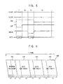
- FIG. 1 illustrates an embodiment of a frame 100 for driving an organic light emitting display device.
- an organic light emitting display device driven by frame 100 may perform a digital driving method that produces grayscale values with a variable time duration for each of a plurality of pixels.
- frame 100 may be divided into at least one refresh sub-frame 110 and a plurality of data sub-frames 120, 130 and 140.
- the refresh sub-frame 110 may include an initializing period T1 during which an emission data voltage is applied to and stored in the plurality of pixels.
- the refresh sub-frame 110 may further include a sensing period T2 during which the degradation of an organic light emitting diode of each pixel is detected.
- Each data sub-frame 120, 130 and 140 may include a scan period T3 during which a scan data voltage is applied to each pixel, and an emission period T4 during which the organic light emitting diode of each pixel emits light.
- T3 during which a scan data voltage is applied to each pixel
- T4 emission period during which the organic light emitting diode of each pixel emits light.
- the frame may include a different number of refresh and/or data sub-frames.
- a switching signal may be applied to the plurality of pixels at substantially the same time, and the emission data voltage may be received and stored from a data driver.
- the emission data voltage may have a voltage level that allows a driving transistor of each pixel to operate in a saturation region and that allows the organic light emitting diode to emit light in response to a driving current generated by the driving transistor.
- the emission data voltage may be adjusted to compensate for degradation of an organic emitting light diode detected during the refresh sub-frame 110 of a previous frame.
- the duration of periods T1 and T2 in the refresh sub-frame are shown to be equal. However, in other embodiments, periods T1 and T2 may have different durations.
- a sensing signal may be applied sequentially row-by-row to the plurality of pixels, and the degradation of the organic light emitting diode of each pixel may be detected to reflect the detected degradation into the emission data voltage of the next frame. Accordingly, since the degradation of the organic light emitting diode is compensated, a life time of the pixel may be increased.
- a scan signal from a scan driver may be applied sequentially row-by-row to the plurality of pixels, and the plurality of pixels may receive and store a scan data voltage transmitted from the data driver.
- the scan data voltage may have a voltage level that allows a third switching transistor coupled in series to the driving transistor to operate in a linear region.
- the scan data voltage applied to each pixel may be either a turn-on voltage that turns on the third switching transistor during the emission period T4 or a turn-off voltage that turns off the third switching transistor during the emission period T4.
- an emission control signal may be applied to the plurality of pixels at substantially the same time, and the organic light emitting diode of each pixel may emit light or not emit light in response to the stored emission data voltage and the stored scan data voltage.
- the plurality of pixels included in the organic light emitting display device may perform simultaneous light emission in response to the emission control signal SGE that is applied to the plurality of pixels at substantially the same time.
- an organic light emitting display device may divide one frame 100 into at least one refresh sub-frame 110 and a plurality of data sub-frames 120, 130 and 140.
- the emission data voltage V_DATA is applied to the driving transistor.
- the emission data voltage V_DATA may have a voltage level that makes the driving transistor operate in the saturation region and that makes the organic light emitting diode emit light.
- the degradation of the organic light emitting diode may be detected and may be reflected into the emission data voltage V_DATA of the next frame. Accordingly, since the degradation of the organic light emitting diode of each pixel is compensated, a life time of the pixel may be increased.
- FIG. 2 is a circuit diagram illustrating an embodiment of a pixel of an organic light emitting display device
- FIG. 3 is a timing diagram for describing operation of a pixel of FIG. 2 .
- a pixel of the organic light emitting display device 200 includes first through third switching transistors 210, 220 and 240, a driving transistor 230, a sensing transistor 250, a leakage current compensating transistor 280, an emission control transistor 260, first and second storage capacitors 292 and 294, and an organic light emitting diode 270.
- the plurality of switching transistors 210, 220 and 240, the driving transistor 230, the sensing transistor 250, the leakage current compensating transistor 280, and the emission control transistor 260 may be implemented as PMOS transistors or NMOS transistors, or a combination of both.
- the first switching transistor 210 may transfer an emission data voltage V_DATA to a first node N1 in response to a switching signal SGC.
- the switching signal SGC may be generated and applied from an external circuit of a display panel or a scan driving part (or a scan driver) of the display panel.
- the switching signal SGC may be applied to the plurality of pixels included in the organic light emitting display device at substantially the same time.
- the switching signal SGC may be applied sequentially row-by-row to the plurality of pixels.
- the first switching transistor 210 may have a gate terminal coupled to a switching line GC_L, a first terminal coupled to a data line DATA_L, and a second terminal coupled to the first node N1.
- the first storage capacitor 292 may store the emission data voltage V_DATA that is transferred to the first node N1 by the first switching transistor 210.
- the emission data voltage V_DATA may have a voltage level that allows the driving transistor 230 to operate in a saturation region and that allows the organic light emitting diode to emit light by a driving current generated by the driving transistor 230.
- the second switching transistor 220 may transfer the scan data voltage V_SCAN to a second node N2 in response to a scan signal SSCAN.
- the scan signal SSCAN may be applied from the scan driver sequentially row-by-row to the plurality of pixels.
- the second switching transistor 220 may have a gate terminal coupled to a scan line SCAN_L, a first terminal coupled to the data line DATA_L, and a second terminal coupled to the second node N2.
- the second storage capacitor 294 may store the scan data voltage V_SCAN that is transferred to the second node N2 by the second switching transistor 220.
- the scan data voltage V_SCAN may have a voltage level that allows the third switching transistor 240 to operate in a linear region and that allows the third switching transistor 240 to be turned on or off in the emission period T4.
- the driving transistor 230 may be turned on in response to the emission data voltage V_DATA stored in the first storage capacitor 292.
- the driving transistor 230 may have a gate terminal coupled to the first node N1, a first terminal coupled to a first power supply voltage ELVDD, and a second terminal coupled to a first terminal of the third switching transistor 240.
- the third switching transistor 240 may control the organic light emitting diode 270 to emit light or not to emit light. This may be accomplished by forming or blocking a path of the driving current flowing, from the first power supply voltage ELVDD through the driving transistor 230, the third switching transistor 240, the emission control transistor 260, and the organic light emitting diode 270, to a second power supply voltage ELVSS based on the scan data voltage V_SCAN stored in the second storage capacitor 294.
- the third switching transistor 240 allows the organic light emitting diode 270 to emit light by forming the path of the driving current. If the scan data voltage V_SCAN stored in the second storage capacitor 294 is a turn-off voltage, the third switching transistor 240 allows the organic light emitting diode 270 not to emit light by blocking the path of the driving current.
- the third switching transistor 240 may have a gate terminal coupled to the second node N2, the first terminal coupled to the second terminal of the driving transistor 230, and a second terminal coupled to a first terminal of the emission control transistor 260.
- the organic light emitting diode 270 may emit light in response to the driving current from the first power supply voltage ELVDD through the driving transistor 230, the third switching transistor 240, emission control transistor 260, and the organic light emitting diode 270 to the second power supply voltage ELVSS.
- the organic light emitting diode 270 may have an anode electrode coupled to a third node N3 and a cathode electrode coupled to the second power supply voltage ELVSS.
- the leakage current compensating transistor 280 may compensate for a black luminance by compensating for the leakage current at the organic light emitting diode 270.
- the leakage current compensating transistor 280 may have a gate terminal coupled to the first power supply voltage ELVDD, a first terminal coupled to the third node N3, and a second terminal coupled to the second power supply voltage ELVSS.
- the sensing transistor 250 may be turned on in response to the sensing signal SSENSE. At this time, the sensing signal SSENSE may be applied from the scan driver sequentially row-by-row to the plurality of pixels.
- the sensing transistor 250 may have a gate terminal coupled to a sensing line SENSE_L, a first terminal coupled to the data line DATA_L, and a second terminal coupled to the anode electrode of the organic light emitting diode 270.
- the emission control transistor 260 may control the organic light emitting diode 270 to emit light or not to emit light. This may be accomplished by forming or blocking the path of the driving current flowing, from the first power supply voltage ELVDD through the driving transistor 230, the third switching transistor 240, the emission control transistor 260, and the organic light emitting diode 270, to the second power supply voltage ELVSS in response to the emission control signal SGE.
- the emission control signal SGE may be generated from an external circuit of the display panel and may be applied to the plurality of pixels at substantially the same time.
- the emission control transistor 260 may have a gate terminal coupled to an emission control line GE_L, a first terminal coupled to the second terminal of the third switching transistor 240, and a second terminal coupled to the anode electrode of the organic light emitting diode 270.
- a frame may be divided into a refresh sub-frame and a plurality of data sub-frames.
- the emission data voltage V_DATA may allow driving transistors 230 of all pixels included in the organic light emitting display device to operate in the saturation region.
- the degradation of the organic light emitting diode 270 may be detected in the refresh sub-frame, and thus the organic light emitting diode 270 may emit light with a desired luminance by compensating for the degradation.
- a low level voltage (e.g., a low gate voltage VGL) may be applied as the switching signal SGC through the switching line GC_L, and the emission data voltage V_DATA may be applied through the data line DL.
- the first switching transistor 210 may transfer the emission data voltage V_DATA to the first node N1 in response to the low gate voltage VGL.
- the first storage capacitor 292 may store charges corresponding to a voltage difference between the first power supply voltage ELVDD and a voltage of the first node N1, or the emission data voltage V_DATA.
- the emission data voltage V_DATA may have a voltage level which allows the driving transistor 230 to operate in the saturation region.
- the low level voltage may be applied as the sensing signal SSENSE through the sensing line SENSE_L, and thus the anode electrode of the organic light emitting diode 270 and the data line DATA_L may be electrically coupled.
- the level of the degradation of the organic light emitting diode 270 may be measured by sensing the current flowing between the anode electrode and the cathode electrode of the organic light emitting diode 270. The measurement may be performed, for example, by an external device.
- the emission data voltage V_DATA of the next frame may be generated by reflecting the measured level of the degradation of the organic light emitting diode 270.
- the degradation of the organic light emitting diode 270 may be compensated using the emission data voltage V_DATA where the measured level of the degradation is reflected.
- the emission control transistor 260 may be turned off by applying a high level voltage (e.g., a high gate voltage VGH) as the emission control signal SGE through the emission control line GE_L, and thus the organic light emitting diode 270 may not emit light.
- a high level voltage e.g., a high gate voltage VGH
- the emission control transistor 260 since the emission control transistor 260 is turned off for the organic light emitting diode 270 not to emit light during the refresh sub-frame 110, an image displayed by the organic light emitting display device may not be affected by the refresh sub-frame 110.
- the emission control signal SGE may be generated and applied from an external device, and the emission control signal SGE may be applied to the plurality of pixels at substantially the same time.
- a low level voltage (e.g., a low gate voltage VGL) may be applied as the scan signal SSCAN through the scan line SL, and the scan data voltage V_SCAN may be applied as the data signal DATA through the data line DL.
- the scan data voltage V_SCAN may have a voltage level corresponding to a value of a corresponding bit of the input data.
- the second switching transistor 220 may transfer the scan data voltage V_SCAN to the second node N2 in response to the low gate voltage VGL.
- the second storage capacitor 294 may store charges corresponding to a voltage difference between the first power supply voltage ELVDD and a voltage of the second node N2, or the scan data voltage V_SCAN.
- the voltage of the second node N2 may be maintained as the scan data voltage V_SCAN even though the second switching transistor 220 is turned off.
- the low level voltage (e.g., low gate voltage VGL) may be applied as the emission control signal SGE through the emission control line GE_L.
- the emission control transistor 260 may be turned on in respond to the low gate voltage VGL. If the driving transistor 230 is turned on by the voltage of the first node N1 (or, the voltage of the second electrode of the first storage capacitor 292), the third switching transistor 240 is turned on by the voltage of the second node N2 (or, the voltage of the second electrode of the second storage capacitor 294), and the emission control transistor 260 is turned on by the low gate voltage VGL, the path of the driving current may be formed.
- the driving current may flow from the first power supply voltage ELVDD (through the path of the driving current including the driving transistor 230, the third switching transistor 240, the emission control transistor 260, and the organic light emitting diode 270) to the second power supply voltage ELVSS.
- the organic light emitting diode 270 may emit light in response to the driving current flowing through the path.
- the emission data voltage V_DATA applied to each pixel is adjusted to compensate for the degradation of the organic light emitting diode 270, the life time of the pixel may be increased.
- FIG. 4 is a circuit diagram illustrating another embodiment of a pixel of an organic light emitting display device
- FIG. 5 is a timing diagram for describing an operation of a pixel of FIG 4 .
- a pixel of the organic light emitting display device 300 includes first through third switching transistors 310, 320 and 340, a driving transistor 330, a leakage current compensating transistor 380, an emission control transistor 360, first and second storage capacitors 392 and 394, and an organic light emitting diode 370.
- the plurality of switching transistors 310, 320 and 340, the driving transistor 330, the leakage current compensating transistor 380, and the emission control transistor 360 may be implemented by PMOS transistors or NMOS transistors, or a combination of both.
- the pixel of the organic light emitting display device 300 may have a configuration and operation similar to the pixel 200 of FIG. 2 , except that a sensing transistor is not included.
- the emission control transistor 360 may be turned off in response to the high gate voltage VGH and an anode electrode of the organic light emitting diode 370 may be coupled directly to an external device.
- the level of the degradation of the organic light emitting diode 370 may be measured by sensing the current flowing between the anode electrode and the cathode electrode of the organic light emitting diode 370. This measurement may be taken by an external device.
- the emission data voltage V_DATA of the next frame may be generated by reflecting the measured level of the degradation of the organic light emitting diode 270.
- the degradation of the organic light emitting diode 370 may be compensated using the emission data voltage V_DATA where the measured level of the degradation is reflected.
- FIG. 6 illustrates another embodiment of a frame for driving an organic light emitting display device.
- an organic light emitting display device 400 performs a digital driving method that produces grayscale values with a variable time duration of each of a plurality of pixels. This is accomplished by dividing a frame into at least one refresh sub-frame 410 and a plurality of data sub-frames 420, 430 and 440.
- the refresh sub-frame 410 may include an initializing period T1 during which an emission data voltage is applied to and stored in each pixel, and a sensing period T2 during which the degradation of an organic light emitting diode of each pixel is detected.
- Each data sub-frame 420, 430 and 440 may include a scan period T3 during which a scan data voltage is applied to and stored in each pixel, and an emission period T4 during which the organic light emitting diode of each pixel emits light.
- T3 scan period
- T4 emission period
- one refresh and three data sub-frames are included.
- a different number of refresh and/or data sub-frames may be included in other embodiments.
- a switching signal SGC may be applied to the plurality of pixels at substantially the same time, and the emission data voltage may be received and stored from the data driver.
- the emission data voltage may have a voltage level that allows a driving transistor of each pixel to operate in saturation region and that allows the organic light emitting diode to emit light in response to a driving current generated by the driving transistor. Further, the emission data voltage may be adjusted to compensate for the degradation of the organic emitting light diode that is detected during the refresh sub-frame 410 of the previous frame.
- a sensing signal may be applied sequentially, row-by-row, to the plurality of pixels.
- the degradation of the organic light emitting diode of each pixel may be detected to reflect the detected degradation into the emission data voltage of the next frame. Accordingly, since the degradation of the organic light emitting diode is compensated, a life time of the pixel may be increased.
- a scan signal from a scan driver may be applied sequentially, row-by-row, to the plurality of pixels.
- the plurality of pixels may receive and store a scan data voltage transmitted from the data driver.
- the scan data voltage may have a voltage level that allows a third switching transistor coupled in series to the driving transistor to operate in a linear region.
- the scan data voltage applied to each pixel may be either a turn-on voltage that turns on the third switching transistor during the emission period T4 or a turn-off voltage that turns off the third switching transistor during the emission period T4.
- an emission control signal may be applied sequentially, row-by-row, to the plurality of pixels.
- the organic light emitting diode of each pixel may emit light or not emit light in response to the stored emission data voltage and the stored scan data voltage.
- the plurality of pixels included the organic light emitting display device may perform sequential light emission in response to the emission control signal SEM that is applied sequentially, row-by-row, to the plurality of pixels.
- an organic light emitting display device may divide one frame 400 into at least one refresh sub-frame 410 and the plurality of data sub-frames 420, 430 and 440.
- the emission data voltage V_DATA having the voltage level that makes the driving transistor operate in the saturation region and that makes the organic light emitting diode emit light may be applied to the driving transistor.
- the degradation of the organic light emitting diode may be detected and may be reflected into the emission data voltage V_DATA of the next frame. Accordingly, since the degradation of the organic light emitting diode of each pixel is compensated, a life time of the pixel may be increased.
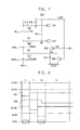
- FIG. 7 illustrates another embodiment of a pixel of an organic light emitting display device
- FIG. 8 is a timing diagram for describing an operation of a pixel of FIG. 7 .
- a pixel of the organic light emitting display device 500 includes first through third switching transistors 510, 520 and 540, a driving transistor 530, a sensing transistor 550, a leakage current compensating transistor 580, an emission control transistor 560, first and second storage capacitor 592 and 594, and an organic light emitting diode 570.
- the plurality of switching transistors 510, 520 and 540, the driving transistor 530, the sensing transistor 550, the leakage current compensating transistor 580, and the emission control transistor 560 may be implemented as PMOS transistors or NMOS transistors, or a combination of both.
- the pixel 500 of FIG. 7 may have configuration and operation similar to the pixel 200 of FIG. 2 , except that an emission control signal is applied sequentially, row-by-row, to the emission control transistor of each pixel through an emission control line.
- the organic light emitting display device that includes pixels of the FIG. 7 may perform sequential light emission in response to the emission control signal that is applied sequentially, row-by-row, to each pixel through the plurality of the emission control line.
- the organic light emitting display device that includes pixels of the FIG. 2 may perform a simultaneous light emission in response to the emission control signal that is applied to each pixel through the emission control line from the external at substantially the same time.
- a low level voltage (e.g., a low gate voltage VGL) may be applied as the scan signal SSCAN, and the second storage capacitor 594 may store charges corresponding to a scan data voltage V_SCAN.
- a high level voltage (e.g., a high gate voltage VGH) may be applied as the emission control signal SEM, and the emission control transistor 560 is turned off. Thus, the organic light emitting diode 570 may not emit light.
- the low level voltage (e.g., low gate voltage VGL) may be applied as the emission control signal SEM through the emission control line EM_L.
- the emission control transistor 560 may be turned on in response to the low gate voltage VGL.
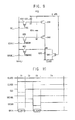
- FIG. 9 illustrates another embodiment of a pixel circuit of an organic light emitting display device
- FIG. 10 is a timing diagram for describing an operation of a pixel of FIG 9 .
- a pixel 600 of the organic light emitting display device may includes first through third switching transistors 610, 620 and 640, a driving transistor 630, a sensing transistor 650, a leakage current compensating transistor 680, first and second storage capacitors 692 and 694, and an organic light emitting diode 670.
- the plurality of switching transistors 610, 620 and 640, the driving transistor 630, the sensing transistor 650, and the leakage current compensating transistor 680 may be implemented by PMOS transistors or NMOS transistors, or a combination of both.
- the pixel 600 of the organic light emitting display device may have configuration and operation similar to the pixel 200 of FIG. 2 , except the emission control transistor is not included.
- a second power supply voltage ELVSS may have the same voltage level as a first power supply voltage ELVDD.
- a current may not be flowing from the first power supply voltage ELVDD to the second power supply voltage ELVSS.
- the organic light emitting diode 670 may not emit light.
- the organic light emitting diode 670 may not emit light by controlling the second power supply voltage ELVSS even though the drain electrode of the third switching transistor 640 and the organic light emitting diode 670 are connected directly.
- an organic light emitting display device may be implemented in various forms.
- a frame for driving the organic light emitting display device may be divided into at least one refresh sub-frame and the plurality of data sub-frames.
- the emission data voltage having the voltage level that makes the driving transistor operate in the saturation region and that makes the organic light emitting diode emit light may be applied to driving transistor.
- the degradation of the organic light emitting diode may be detected and may be reflected into the emission data voltage of the next frame. Accordingly, since the degradation of the organic light emitting diode is compensated, a life time of the pixel may be increased.
- FIG. 11 illustrates an embodiment of an organic light emitting display device 700 which includes a pixel unit 710 containing at least one pixel and PX the driving unit 750.
- the pixel unit 710 may be coupled to the data driver 760 of the driving unit 750 through a plurality of data lines, may be coupled to the scan driver 770 of the driving unit 750 through a plurality of scan lines and a plurality of sensing lines, and may be coupled to the emission control driver 780 of the driving unit 750 through a plurality of emission control lines.
- the pixel unit 710 may include a plurality of pixels PX located at crossing points of the plurality of data lines and the plurality of scan lines.
- the driving unit 750 may apply an emission data voltage V_DATA which makes the driving transistor operate in a saturation region and may apply a scan data voltage V_SCAN which makes the organic light emitting diode turn on or turn off to each pixel PX of the pixel unit 710. During one frame, the driving unit 750 may produce grayscale values with a variable time duration of each of a plurality of pixels PX.
- the driving unit 750 may drive the pixel unit 710 based on a frame divided into one refresh sub-frame and a plurality of data sub-frames. For example, the driving unit 750 may receive the input data about each pixel PX of the pixel unit 710, may divide one frame into one refresh sub-frame and the plurality of data sub-frames, and may apply the emission data voltage V_DATA corresponding to a value of a corresponding bit of the input data in the refresh sub-frame. At this time, the emission data voltage V_DATA may have a level which makes the driving transistor operate in the saturation region and which makes the organic light emitting diode emit light. Also, in each data sub-frame, the driving unit 750 may apply the scan data voltage V_SCAN.
- the driving unit 750 includes a data driver 760, a scan driver 770, and an emission control driver 780.
- the data driver 760 may apply the emission data voltage V_DATA to the pixel unit 710 through the plurality of data lines in each refresh sub-frame and may apply the scan data voltage V_SCAN to the pixel unit 710 through the data lines in each data sub-frame.
- the scan driver 770 may apply the scan signal SSCAN to the pixel unit 710 through the plurality of scan lines and may apply the sensing signal SSENSE to the pixel unit 710 through the plurality of sensing lines.
- the emission control driver 780 may apply the emission control signal SEM to the pixel unit 710 through the plurality of emission control lines.
- the timing controller 790 may control an operation of the organic light emitting display device 700.
- the timing controller 790 may control the operation of the organic light emitting diode 700 by providing control signals to the data driver 760, the scan driver 770 and the emission control driver 780.
- data driver 760, scan driver 770, emission control driver 780, and the timing controller 760 may be implemented with an integrated circuit IC.
- data driver 760, scan driver 770, emission control driver 780, and the timing controller 760 may be implemented with two or more integrated circuits IC.
Landscapes
- Engineering & Computer Science (AREA)
- Physics & Mathematics (AREA)
- General Physics & Mathematics (AREA)
- Theoretical Computer Science (AREA)
- Computer Hardware Design (AREA)
- Microelectronics & Electronic Packaging (AREA)
- Geometry (AREA)
- Control Of El Displays (AREA)
- Control Of Indicators Other Than Cathode Ray Tubes (AREA)
- Electroluminescent Light Sources (AREA)
Applications Claiming Priority (1)
| Application Number | Priority Date | Filing Date | Title |
|---|---|---|---|
| KR1020130052925A KR20140133189A (ko) | 2013-05-10 | 2013-05-10 | 유기 발광 표시 장치의 화소 및 유기 발광 표시 장치 |
Publications (1)
| Publication Number | Publication Date |
|---|---|
| EP2801969A1 true EP2801969A1 (de) | 2014-11-12 |
Family
ID=50389359
Family Applications (1)
| Application Number | Title | Priority Date | Filing Date |
|---|---|---|---|
| EP14162813.1A Withdrawn EP2801969A1 (de) | 2013-05-10 | 2014-03-31 | Pixel einer organischen lichtemittierenden Anzeigevorrichtung und organische lichtemittierende Anzeigevorrichtung |
Country Status (5)
| Country | Link |
|---|---|
| US (1) | US20140333680A1 (de) |
| EP (1) | EP2801969A1 (de) |
| KR (1) | KR20140133189A (de) |
| CN (1) | CN104143312B (de) |
| TW (1) | TW201503084A (de) |
Cited By (3)
| Publication number | Priority date | Publication date | Assignee | Title |
|---|---|---|---|---|
| US10672315B2 (en) | 2016-08-08 | 2020-06-02 | Hefei Xinsheng Optoelectronics Technology Co., Ltd. | Array substrate, display panel, display apparatus and current measuring method |
| CN113053313A (zh) * | 2021-03-26 | 2021-06-29 | 苏州科达科技股份有限公司 | Oled屏幕残影减少方法、系统、设备及存储介质 |
| EP3816978A4 (de) * | 2018-06-29 | 2022-07-20 | Boe Technology Group Co., Ltd. | Ansteuerungsschaltung und ansteuerungsverfahren dafür sowie anzeigevorrichtung |
Families Citing this family (35)
| Publication number | Priority date | Publication date | Assignee | Title |
|---|---|---|---|---|
| KR102168879B1 (ko) * | 2014-07-10 | 2020-10-23 | 엘지디스플레이 주식회사 | 유기발광다이오드의 열화를 센싱할 수 있는 유기발광 표시장치 |
| KR102218642B1 (ko) * | 2014-11-27 | 2021-02-23 | 삼성디스플레이 주식회사 | 표시 장치 및 표시 장치의 구동 방법 |
| KR102349175B1 (ko) | 2015-06-11 | 2022-01-11 | 삼성디스플레이 주식회사 | 영상 데이터의 프레임 구조 및 이를 이용한 유기 발광 표시 장치의 디지털 구동 방법 |
| KR102411075B1 (ko) * | 2015-08-24 | 2022-06-21 | 삼성디스플레이 주식회사 | 화소 회로 및 이를 포함하는 유기 발광 표시 장치 |
| KR102383741B1 (ko) * | 2015-09-10 | 2022-04-08 | 삼성디스플레이 주식회사 | 화소, 화소를 포함하는 유기전계발광 표시장치 및 화소의 구동 방법 |
| CN106920801B (zh) * | 2015-12-24 | 2020-07-14 | 群创光电股份有限公司 | 显示装置 |
| US10297191B2 (en) | 2016-01-29 | 2019-05-21 | Samsung Display Co., Ltd. | Dynamic net power control for OLED and local dimming LCD displays |
| DE112017003050B4 (de) * | 2016-06-20 | 2026-05-07 | Sony Corporation | Anzeigeeinrichtung und elektronische Einrichtung |
| KR102316564B1 (ko) * | 2017-05-29 | 2021-10-25 | 엘지디스플레이 주식회사 | 유기 발광 다이오드 디스플레이 장치 및 유기발광 다이오드 디스플레이 장치의 보상 데이터 처리 방법 |
| KR102413866B1 (ko) * | 2017-08-16 | 2022-06-27 | 엘지디스플레이 주식회사 | 유기 발광 표시 장치와 그의 구동 방법 |
| KR102398553B1 (ko) * | 2017-08-29 | 2022-05-17 | 엘지디스플레이 주식회사 | 유기발광 표시장치 |
| CN107492342B (zh) * | 2017-09-19 | 2020-07-03 | 深圳市华星光电半导体显示技术有限公司 | 一种显示面板实时sense的驱动方法及显示装置 |
| KR102472310B1 (ko) * | 2017-09-27 | 2022-11-30 | 삼성디스플레이 주식회사 | 유기 발광 표시 장치 |
| CN107507567B (zh) * | 2017-10-18 | 2019-06-07 | 京东方科技集团股份有限公司 | 一种像素补偿电路、其驱动方法及显示装置 |
| KR102518747B1 (ko) * | 2017-12-28 | 2023-04-07 | 삼성디스플레이 주식회사 | 유기전계발광 표시장치 및 그의 구동방법 |
| CN108520716B (zh) * | 2018-04-12 | 2019-10-01 | 京东方科技集团股份有限公司 | 一种像素电路单元及驱动方法、显示面板、显示装置 |
| CN110400538B (zh) * | 2018-04-19 | 2021-02-09 | 群创光电股份有限公司 | 电子装置 |
| CN110473496B (zh) * | 2018-05-09 | 2021-01-26 | 京东方科技集团股份有限公司 | 像素电路及其驱动方法、显示基板、显示装置 |
| CN108766360B (zh) * | 2018-05-23 | 2020-04-10 | 京东方科技集团股份有限公司 | 显示面板的驱动方法和显示装置 |
| CN108962106B (zh) * | 2018-07-13 | 2022-02-22 | 京东方科技集团股份有限公司 | 一种像素检测电路、显示基板及像素检测方法 |
| WO2020071826A1 (ko) | 2018-10-04 | 2020-04-09 | 삼성전자주식회사 | 정전류 설정 구성을 갖는 표시 장치 및 그 구동 방법 |
| JP7154928B2 (ja) * | 2018-10-04 | 2022-10-18 | 三星電子株式会社 | 表示装置、駆動回路、及び、表示装置の駆動方法 |
| KR102085516B1 (ko) * | 2019-05-01 | 2020-03-05 | 주식회사 티엘아이 | 효율적인 열화 보상 구조를 가지는 유기발광 디스플레이 장치 |
| TWI692749B (zh) * | 2019-05-21 | 2020-05-01 | 友達光電股份有限公司 | 驅動方法及顯示裝置 |
| KR102656469B1 (ko) * | 2019-07-09 | 2024-04-12 | 삼성디스플레이 주식회사 | 유기 발광 표시 장치의 화소, 및 유기 발광 표시 장치 |
| CN110517641B (zh) * | 2019-08-30 | 2021-05-14 | 京东方科技集团股份有限公司 | 像素电路、参数检测方法、显示面板和显示装置 |
| CN111063295B (zh) * | 2019-12-31 | 2021-05-07 | 深圳市华星光电半导体显示技术有限公司 | 一种发光二极管阵列面板的驱动装置及其驱动方法 |
| KR102812880B1 (ko) * | 2020-10-30 | 2025-05-27 | 삼성디스플레이 주식회사 | 표시 장치 |
| CN113539163B (zh) * | 2021-07-16 | 2024-03-19 | 北京京东方显示技术有限公司 | 显示基板、显示面板和显示装置 |
| KR102907790B1 (ko) * | 2021-11-24 | 2026-01-06 | 보에 테크놀로지 그룹 컴퍼니 리미티드 | 표시 기판, 그 구동 방법 및 표시 장치 |
| KR20230158142A (ko) * | 2022-05-10 | 2023-11-20 | 삼성디스플레이 주식회사 | 표시 장치와 그의 구동 방법 |
| US12062303B2 (en) * | 2022-05-31 | 2024-08-13 | Chip Design Systems Inc. | LED driver circuitry for an infrared scene projector system |
| CN115035854A (zh) * | 2022-06-24 | 2022-09-09 | 惠科股份有限公司 | 像素驱动电路、驱动方法和显示装置 |
| CN116741104B (zh) * | 2023-04-13 | 2025-10-10 | 天马微电子股份有限公司 | 像素驱动电路、驱动方法、显示面板及显示装置 |
| CN119152797B (zh) * | 2023-06-16 | 2025-09-02 | 武汉华星光电半导体显示技术有限公司 | 显示背板及显示装置 |
Citations (4)
| Publication number | Priority date | Publication date | Assignee | Title |
|---|---|---|---|---|
| US20050225683A1 (en) * | 2004-04-12 | 2005-10-13 | Seiko Epson Corporation | Electro-optical device and electronic apparatus |
| WO2007042973A1 (en) * | 2005-10-13 | 2007-04-19 | Koninklijke Philips Electronics N.V. | Emissive display devices |
| US20080284688A1 (en) * | 2004-06-11 | 2008-11-20 | Thilo Marx | Method for Driving, and a Circuit of an Element of an Illuminated Display |
| US20110205250A1 (en) * | 2010-02-23 | 2011-08-25 | Samsung Mobile Display Co., Ltd. | Organic Light Emitting Display and Driving Method Thereof |
Family Cites Families (5)
| Publication number | Priority date | Publication date | Assignee | Title |
|---|---|---|---|---|
| KR100902219B1 (ko) * | 2007-12-05 | 2009-06-11 | 삼성모바일디스플레이주식회사 | 유기전계발광 표시장치 |
| KR101938880B1 (ko) * | 2011-11-18 | 2019-01-16 | 엘지디스플레이 주식회사 | 유기발광다이오드 표시장치 |
| KR101517035B1 (ko) * | 2011-12-05 | 2015-05-06 | 엘지디스플레이 주식회사 | 유기발광 다이오드 표시장치 및 그 구동방법 |
| KR101893167B1 (ko) * | 2012-03-23 | 2018-10-05 | 삼성디스플레이 주식회사 | 화소 회로, 이의 구동 방법 및 유기 발광 표시 장치 |
| KR101987424B1 (ko) * | 2012-11-29 | 2019-06-11 | 삼성디스플레이 주식회사 | 화소 및 이를 포함하는 표시 장치, 및 그 구동 방법 |
-
2013
- 2013-05-10 KR KR1020130052925A patent/KR20140133189A/ko not_active Ceased
-
2014
- 2014-01-30 US US14/168,500 patent/US20140333680A1/en not_active Abandoned
- 2014-03-25 TW TW103111135A patent/TW201503084A/zh unknown
- 2014-03-31 EP EP14162813.1A patent/EP2801969A1/de not_active Withdrawn
- 2014-04-24 CN CN201410168672.3A patent/CN104143312B/zh active Active
Patent Citations (4)
| Publication number | Priority date | Publication date | Assignee | Title |
|---|---|---|---|---|
| US20050225683A1 (en) * | 2004-04-12 | 2005-10-13 | Seiko Epson Corporation | Electro-optical device and electronic apparatus |
| US20080284688A1 (en) * | 2004-06-11 | 2008-11-20 | Thilo Marx | Method for Driving, and a Circuit of an Element of an Illuminated Display |
| WO2007042973A1 (en) * | 2005-10-13 | 2007-04-19 | Koninklijke Philips Electronics N.V. | Emissive display devices |
| US20110205250A1 (en) * | 2010-02-23 | 2011-08-25 | Samsung Mobile Display Co., Ltd. | Organic Light Emitting Display and Driving Method Thereof |
Non-Patent Citations (1)
| Title |
|---|
| MIN U-G ET AL: "Real-time external sensing and compensation method for organic light emitting diode displays", ELECTRONIC LETTERS, THE INSTITUTION OF ENGINEERING AND TECHNOLOGY, vol. 45, no. 24, 19 November 2009 (2009-11-19), pages 1232 - 1234, XP006034313, ISSN: 1350-911X, DOI: 10.1049/EL:20091165 * |
Cited By (4)
| Publication number | Priority date | Publication date | Assignee | Title |
|---|---|---|---|---|
| US10672315B2 (en) | 2016-08-08 | 2020-06-02 | Hefei Xinsheng Optoelectronics Technology Co., Ltd. | Array substrate, display panel, display apparatus and current measuring method |
| EP3816978A4 (de) * | 2018-06-29 | 2022-07-20 | Boe Technology Group Co., Ltd. | Ansteuerungsschaltung und ansteuerungsverfahren dafür sowie anzeigevorrichtung |
| CN113053313A (zh) * | 2021-03-26 | 2021-06-29 | 苏州科达科技股份有限公司 | Oled屏幕残影减少方法、系统、设备及存储介质 |
| CN113053313B (zh) * | 2021-03-26 | 2022-08-02 | 苏州科达科技股份有限公司 | Oled屏幕残影减少方法、系统、设备及存储介质 |
Also Published As
| Publication number | Publication date |
|---|---|
| CN104143312A (zh) | 2014-11-12 |
| TW201503084A (zh) | 2015-01-16 |
| CN104143312B (zh) | 2018-03-16 |
| KR20140133189A (ko) | 2014-11-19 |
| US20140333680A1 (en) | 2014-11-13 |
Similar Documents
| Publication | Publication Date | Title |
|---|---|---|
| US20140333680A1 (en) | Pixel of an organic light emitting display device and organic light emitting display device | |
| KR101932744B1 (ko) | 픽셀 회로, 이를 위한 구동 방법 및 능동형 유기 발광 디스플레이 | |
| JP4887334B2 (ja) | エミッション駆動部及び有機電界発光表示装置 | |
| US9647047B2 (en) | Organic light emitting display for initializing pixels | |
| CN102047312B (zh) | 图像显示装置及其驱动方法 | |
| KR101528147B1 (ko) | 발광표시장치 | |
| US20190096330A1 (en) | Organic light emitting display device | |
| JP4630789B2 (ja) | 発光表示装置,及び画素回路 | |
| US9633625B2 (en) | Pixel circuit and method for driving the same | |
| KR102763628B1 (ko) | 에미션 구동부, 이를 포함하는 표시 장치 및 이를 이용한 표시 장치의 구동 방법 | |
| US20170365211A1 (en) | Stage and organic light emitting display device using the same | |
| US9792853B2 (en) | Pixel, driving method of pixel, and display device including pixel | |
| US20190012948A1 (en) | Pixel circuit, and display device and driving method therefor | |
| US10504440B2 (en) | Pixel circuit, driving method thereof, display panel and display apparatus | |
| US9633598B2 (en) | Pixel circuit and driving method thereof | |
| US10692440B2 (en) | Pixel and organic light emitting display device including the same | |
| US9633605B2 (en) | Pixel circuit having driving method for threshold compensation and display apparatus having the same | |
| KR20170132016A (ko) | Oled 표시 장치 및 그의 구동 방법 | |
| US9852690B2 (en) | Drive method and display device | |
| KR20180062276A (ko) | 유기 발광 다이오드 표시 장치 | |
| KR20180003387A (ko) | 유기발광 표시장치 및 그의 구동 방법 | |
| JP2014109703A (ja) | 表示装置および駆動方法 | |
| CN104167167A (zh) | 像素电路及其驱动方法、显示装置 | |
| US20140320476A1 (en) | Pixel and organic light emitting display device using the same | |
| JP2014038168A (ja) | 表示装置、電子機器、駆動方法および駆動回路 |
Legal Events
| Date | Code | Title | Description |
|---|---|---|---|
| PUAI | Public reference made under article 153(3) epc to a published international application that has entered the european phase |
Free format text: ORIGINAL CODE: 0009012 |
|
| 17P | Request for examination filed |
Effective date: 20140331 |
|
| AK | Designated contracting states |
Kind code of ref document: A1 Designated state(s): AL AT BE BG CH CY CZ DE DK EE ES FI FR GB GR HR HU IE IS IT LI LT LU LV MC MK MT NL NO PL PT RO RS SE SI SK SM TR |
|
| AX | Request for extension of the european patent |
Extension state: BA ME |
|
| RAP1 | Party data changed (applicant data changed or rights of an application transferred) |
Owner name: SAMSUNG DISPLAY CO., LTD. |
|
| STAA | Information on the status of an ep patent application or granted ep patent |
Free format text: STATUS: THE APPLICATION IS DEEMED TO BE WITHDRAWN |
|
| 18D | Application deemed to be withdrawn |
Effective date: 20150513 |