EP2802007A1 - Module de puissance à semi-conducteur - Google Patents
Module de puissance à semi-conducteur Download PDFInfo
- Publication number
- EP2802007A1 EP2802007A1 EP20130166986 EP13166986A EP2802007A1 EP 2802007 A1 EP2802007 A1 EP 2802007A1 EP 20130166986 EP20130166986 EP 20130166986 EP 13166986 A EP13166986 A EP 13166986A EP 2802007 A1 EP2802007 A1 EP 2802007A1
- Authority
- EP
- European Patent Office
- Prior art keywords
- power semiconductor
- bond wire
- bond
- semiconductor device
- circuit path
- Prior art date
- Legal status (The legal status is an assumption and is not a legal conclusion. Google has not performed a legal analysis and makes no representation as to the accuracy of the status listed.)
- Withdrawn
Links
Images


Classifications
-
- H—ELECTRICITY
- H10—SEMICONDUCTOR DEVICES; ELECTRIC SOLID-STATE DEVICES NOT OTHERWISE PROVIDED FOR
- H10W—GENERIC PACKAGES, INTERCONNECTIONS, CONNECTORS OR OTHER CONSTRUCTIONAL DETAILS OF DEVICES COVERED BY CLASS H10
- H10W72/00—Interconnections or connectors in packages
- H10W72/50—Bond wires
-
- H—ELECTRICITY
- H10—SEMICONDUCTOR DEVICES; ELECTRIC SOLID-STATE DEVICES NOT OTHERWISE PROVIDED FOR
- H10W—GENERIC PACKAGES, INTERCONNECTIONS, CONNECTORS OR OTHER CONSTRUCTIONAL DETAILS OF DEVICES COVERED BY CLASS H10
- H10W72/00—Interconnections or connectors in packages
- H10W72/071—Connecting or disconnecting
- H10W72/075—Connecting or disconnecting of bond wires
- H10W72/07551—Connecting or disconnecting of bond wires characterised by changes in properties of the bond wires during the connecting
- H10W72/07553—Connecting or disconnecting of bond wires characterised by changes in properties of the bond wires during the connecting changes in shapes
-
- H—ELECTRICITY
- H10—SEMICONDUCTOR DEVICES; ELECTRIC SOLID-STATE DEVICES NOT OTHERWISE PROVIDED FOR
- H10W—GENERIC PACKAGES, INTERCONNECTIONS, CONNECTORS OR OTHER CONSTRUCTIONAL DETAILS OF DEVICES COVERED BY CLASS H10
- H10W72/00—Interconnections or connectors in packages
- H10W72/071—Connecting or disconnecting
- H10W72/075—Connecting or disconnecting of bond wires
- H10W72/07551—Connecting or disconnecting of bond wires characterised by changes in properties of the bond wires during the connecting
- H10W72/07554—Connecting or disconnecting of bond wires characterised by changes in properties of the bond wires during the connecting changes in dispositions
-
- H—ELECTRICITY
- H10—SEMICONDUCTOR DEVICES; ELECTRIC SOLID-STATE DEVICES NOT OTHERWISE PROVIDED FOR
- H10W—GENERIC PACKAGES, INTERCONNECTIONS, CONNECTORS OR OTHER CONSTRUCTIONAL DETAILS OF DEVICES COVERED BY CLASS H10
- H10W72/00—Interconnections or connectors in packages
- H10W72/50—Bond wires
- H10W72/531—Shapes of wire connectors
- H10W72/5363—Shapes of wire connectors the connected ends being wedge-shaped
-
- H—ELECTRICITY
- H10—SEMICONDUCTOR DEVICES; ELECTRIC SOLID-STATE DEVICES NOT OTHERWISE PROVIDED FOR
- H10W—GENERIC PACKAGES, INTERCONNECTIONS, CONNECTORS OR OTHER CONSTRUCTIONAL DETAILS OF DEVICES COVERED BY CLASS H10
- H10W72/00—Interconnections or connectors in packages
- H10W72/50—Bond wires
- H10W72/541—Dispositions of bond wires
- H10W72/5438—Dispositions of bond wires the bond wires having multiple connections on the same bond pad
-
- H—ELECTRICITY
- H10—SEMICONDUCTOR DEVICES; ELECTRIC SOLID-STATE DEVICES NOT OTHERWISE PROVIDED FOR
- H10W—GENERIC PACKAGES, INTERCONNECTIONS, CONNECTORS OR OTHER CONSTRUCTIONAL DETAILS OF DEVICES COVERED BY CLASS H10
- H10W72/00—Interconnections or connectors in packages
- H10W72/50—Bond wires
- H10W72/541—Dispositions of bond wires
- H10W72/547—Dispositions of multiple bond wires
- H10W72/5473—Dispositions of multiple bond wires multiple bond wires connected to a common bond pad
-
- H—ELECTRICITY
- H10—SEMICONDUCTOR DEVICES; ELECTRIC SOLID-STATE DEVICES NOT OTHERWISE PROVIDED FOR
- H10W—GENERIC PACKAGES, INTERCONNECTIONS, CONNECTORS OR OTHER CONSTRUCTIONAL DETAILS OF DEVICES COVERED BY CLASS H10
- H10W72/00—Interconnections or connectors in packages
- H10W72/50—Bond wires
- H10W72/541—Dispositions of bond wires
- H10W72/547—Dispositions of multiple bond wires
- H10W72/5475—Dispositions of multiple bond wires multiple bond wires connected to common bond pads at both ends of the wires
-
- H—ELECTRICITY
- H10—SEMICONDUCTOR DEVICES; ELECTRIC SOLID-STATE DEVICES NOT OTHERWISE PROVIDED FOR
- H10W—GENERIC PACKAGES, INTERCONNECTIONS, CONNECTORS OR OTHER CONSTRUCTIONAL DETAILS OF DEVICES COVERED BY CLASS H10
- H10W72/00—Interconnections or connectors in packages
- H10W72/50—Bond wires
- H10W72/551—Materials of bond wires
- H10W72/552—Materials of bond wires comprising metals or metalloids, e.g. silver
- H10W72/5524—Materials of bond wires comprising metals or metalloids, e.g. silver comprising aluminium [Al]
-
- H—ELECTRICITY
- H10—SEMICONDUCTOR DEVICES; ELECTRIC SOLID-STATE DEVICES NOT OTHERWISE PROVIDED FOR
- H10W—GENERIC PACKAGES, INTERCONNECTIONS, CONNECTORS OR OTHER CONSTRUCTIONAL DETAILS OF DEVICES COVERED BY CLASS H10
- H10W72/00—Interconnections or connectors in packages
- H10W72/851—Dispositions of multiple connectors or interconnections
- H10W72/874—On different surfaces
- H10W72/884—Die-attach connectors and bond wires
-
- H—ELECTRICITY
- H10—SEMICONDUCTOR DEVICES; ELECTRIC SOLID-STATE DEVICES NOT OTHERWISE PROVIDED FOR
- H10W—GENERIC PACKAGES, INTERCONNECTIONS, CONNECTORS OR OTHER CONSTRUCTIONAL DETAILS OF DEVICES COVERED BY CLASS H10
- H10W72/00—Interconnections or connectors in packages
- H10W72/90—Bond pads, in general
- H10W72/921—Structures or relative sizes of bond pads
- H10W72/926—Multiple bond pads having different sizes
-
- H—ELECTRICITY
- H10—SEMICONDUCTOR DEVICES; ELECTRIC SOLID-STATE DEVICES NOT OTHERWISE PROVIDED FOR
- H10W—GENERIC PACKAGES, INTERCONNECTIONS, CONNECTORS OR OTHER CONSTRUCTIONAL DETAILS OF DEVICES COVERED BY CLASS H10
- H10W72/00—Interconnections or connectors in packages
- H10W72/90—Bond pads, in general
- H10W72/931—Shapes of bond pads
- H10W72/932—Plan-view shape, i.e. in top view
-
- H—ELECTRICITY
- H10—SEMICONDUCTOR DEVICES; ELECTRIC SOLID-STATE DEVICES NOT OTHERWISE PROVIDED FOR
- H10W—GENERIC PACKAGES, INTERCONNECTIONS, CONNECTORS OR OTHER CONSTRUCTIONAL DETAILS OF DEVICES COVERED BY CLASS H10
- H10W90/00—Package configurations
- H10W90/701—Package configurations characterised by the relative positions of pads or connectors relative to package parts
- H10W90/731—Package configurations characterised by the relative positions of pads or connectors relative to package parts of die-attach connectors
- H10W90/734—Package configurations characterised by the relative positions of pads or connectors relative to package parts of die-attach connectors between a chip and a stacked insulating package substrate, interposer or RDL
-
- H—ELECTRICITY
- H10—SEMICONDUCTOR DEVICES; ELECTRIC SOLID-STATE DEVICES NOT OTHERWISE PROVIDED FOR
- H10W—GENERIC PACKAGES, INTERCONNECTIONS, CONNECTORS OR OTHER CONSTRUCTIONAL DETAILS OF DEVICES COVERED BY CLASS H10
- H10W90/00—Package configurations
- H10W90/701—Package configurations characterised by the relative positions of pads or connectors relative to package parts
- H10W90/751—Package configurations characterised by the relative positions of pads or connectors relative to package parts of bond wires
- H10W90/754—Package configurations characterised by the relative positions of pads or connectors relative to package parts of bond wires between a chip and a stacked insulating package substrate, interposer or RDL
Definitions
- the Invention relates to a power semiconductor module.
- the invention relates to a power semiconductor module comprising at least one power semiconductor device with an improved electrical connection to a circuit path.
- the present invention further relates to a power semiconductor arrangement comprising such a power semiconductor module.
- Power semiconductor modules comprise a substrate with a plurality of circuit paths on which power semiconductor devices are arranged and connected thereto, respectively. Often, these semiconductor devices are connected to circuit paths by means of bond wires. Secure bond wiring thereby contributes to long term stability as well as safety of the power semiconductor modules.
- EP 2 159 834 A1 is a semiconductor device which comprises an electrical connection with a plurality of bond wire feet connecting a chip of the semiconductor device.
- each foot has a coating that attaches the bond wire to the chip, wherein the coating is electrically conductive.
- a power semiconductor module comprising a bonded electrical connection of a power semiconductor device to a circuit path.
- the bonding connection comprises a plurality of bond wires, wherein a plurality of bond feet of adjacent bond wires is arranged in a chessboard-like manner.
- a power semiconductor module providing an improved long-term stability and/or security.
- the invention relates to a power semiconductor module comprising a substrate, on which substrate at least one power semiconductor device is located, wherein the at least one power semiconductor device is electrically connected to a circuit path via at least one bond wire, wherein at least one bond wire comprises at least two bond wire feet for attaching the bond wire to a contact of the power semiconductor device, wherein the bond wire has a diameter d 1 , and wherein the contact is at least partly surrounded by a termination, wherein a first bond wire foot is located at a distance d 2 to the termination, and wherein the distance d 2 between the termination and the first bond wire foot lies in the range of d 2 ⁇ 1,5d 1 to d 2 ⁇ 6d 1 .
- Such a power semiconductor module may provide an improved long-term stability and thus reliability and additionally improved security behaviour.
- the power semiconductor module comprises a substrate, on which substrate at least one power semiconductor device is located.
- the substrate may generally be any substrate known in the art for power semiconductor modules.
- the substrate may be formed of an insulating material, such as of a ceramic material.
- the substrate may be formed from aluminium nitride (AIN), silicon nitride (Si 3 N 4 ) or aluminium oxide (Al 2 O 3 ).
- AIN aluminium nitride
- Si 3 N 4 silicon nitride
- Al 2 O 3 aluminium oxide
- a plurality of circuit paths may be provided like generally known in the art.
- Such circuit paths may for example be formed from a metallization, such as a copper metallization.
- the metal, such as the copper may be arranged on the substrate by physical or chemical deposition methods, for example.
- At least one, preferably a plurality of power semiconductor devices is arranged on the substrate, or a circuit path, respectively, and electrically connected thereto by means of their collector contact. Further the power semiconductor devices are connected via their emitter contact to a further circuit path, such as to the circuit path carrying the load current, via at least one bond wire.
- a plurality of bond wires may be provided in order to electrically connect a power semiconductor device, or its emitter contact, respectively, with said circuit path.
- the power semiconductor device may generally be provided as known in the art for power semiconductor modules, or power semiconductor arrangements, respectively.
- the power semiconductor device may be an insulated gate bipolar transistor (IGBT), a reverse conductive insulated gate bipolar transistor (reverse conducting IGBT), bi-mode insulated gate transistor (BIGT) and /or a diode, such as a Schottky diode.
- IGBT insulated gate bipolar transistor
- BIGT bi-mode insulated gate transistor
- a diode such as a Schottky diode.
- more than one semiconductor device may be present.
- a plurality of the same or of different power semiconductor devices may be present.
- an IGBT and a diode may be present in one module.
- a power semiconductor device may be particularly suitable for power electronics which may exemplary and typicaly refer to applications working with currents of more than approximately 74A and voltages of more than approximately 100V, the before named values being exemplary values only.
- the latter is arranged by at least one bond wire such as by an aluminium bond wire.
- the bond wire has a diameter d 1 .
- Such a diameter may particularly be the average diameter of the bond wire. This may be the case both for exactly round bond wires as well as for bond wires deviating from the exact round form and thus cross-section. Especially in the latter case the diameter shall be the averaged diameter taking into consideration all thicknesses of the diameter. It is thereby noted that the diameter of the pure bond wire is meant, without any additional parts, such as bond wire feet, like will be described down below.
- the bond wire comprises at least two bond wire feet for attaching the bond wire to a surface of the power semiconductor device, or its emitter contact, respectively.
- a wire foot is particularly a connection point of the bond wire to the semiconductor device, or its contact, respectively.
- the bond wire is fixed to the power semiconductor device, or its contact, respectively, these connection points being called bond wire feet.
- the latter arrangement may be described as a so-called stitch-bonding.
- the bond wire is attached to the power semiconductor device, or its contact, respectively, by welding.
- the bond wire feet are formed by welding the bond wire to the surface of the power semiconductor device.
- the bond wire may be attached and fixed to the surface of the power semiconductor device in an especially easy and cost-saving manner which also allows an automated manufacturing process.
- the bond wire feet are formed such that the current may flow through the respective feet without major resistivity. As a result, the heat formation due to high currents may be strongly reduced so that the reliability as well as security behaviour may be additionally improved.
- a plurality of bond wire feet are arranged subsequently essentially in a direction from the edge of the contact of the power semiconductor device, or its surface, respectively, being directed towards the circuit path, to the opposite direction of the power semiconductor device.
- the bond wire foot being located closest to the edge of the contact of the power semiconductor device being directed towards the circuit path, which in the further application is called the first bond wire foot, is located at a distance d 2 to a termination of the power semiconductor device.
- a termination of the power semiconductor device may particularly be a feature which as well may be called a guard ring and it may be formed as a one part structure or it may be formed as a multi-part structure as it is generally known for one skilled in the art.
- the termination may have the potential of the collector electrode and thus a different potential compared to the emitter electrode which is connected by the bond wires.
- the distance d 2 of the first bond wire foot to the termination of the power semiconductor device and thus the location of the first bond wire foot is chosen in dependence of the diameter of the bond wire. According to this, a plurality of advantages may be achieved.
- power semiconductor devices may provide elevated temperatures, or generate heat, respectively, during an operation of the power semiconductor module, or the power semiconductor device, respectively.
- the heat may be generated in a comparably greater amount at the centre, or the middle part, respectively, of the power semiconductor device, whereas the edge may provide a comparably cooler temperature. Therefore, due to the comparably low length of d 2 , the heat influence to the bond wire feet is significantly lowered and in fact under circumstances the bond wire may be cooled by the surface of the power semiconductor device. According to this, the stability of the bonding connection is as well significantly improved.
- the above further allows the module to be less sensitive against temperature cycling and thus power cycling.
- This in turn allows providing a significantly improved long-term stability and thus reliability. This may be especially advantageous due to the fact that depending on the specific application, rather long service-free working times of the power semiconductor modules are required. In case a module fails, however, time-intensive as well as cost-intensive measures are required which may be avoided or at least reduced according to the invention.
- a module like described above may further provide the capability of withstanding even higher currents being used. This may be especially advantageous with respect to the fact the especially the capability of carrying current in combination with temperature management may be important for being suitable for high class applications using high currents and high voltages.
- At least one bond wire has a diameter d 1 in the range of ⁇ 300 ⁇ m to ⁇ 500 ⁇ m.
- at least one bond wire has a diameter in the range of ⁇ 370 ⁇ m to ⁇ 410 ⁇ m, for example 385 ⁇ m.
- all bond wires present connecting the contact of one or more than one power semiconductor devices with a circuit path have the afore-mentioned diameters.
- the bond wires are arranged for withstanding even high currents making them suitable especially for power semiconductor applications. Further, these diameters d 1 and accordingly the distance d 2 may provide an especially preferred resistance against temperature and further temperature cycling allowing an especially good reliability as well as security for power applications.
- a minimum distance d 3 between the edge of the contact being directed towards the circuit path and the bond wire in a perpendicular direction of the edge of the contact lies in the range of ⁇ (voltage used/3KV) * 1 mm to ⁇ 3mm + (voltage used/3KV) * 1 mm.
- appropriate voltages being used by a performance of the respective power semiconductor module may in a non-limiting example be in the range of ⁇ 1,7kV to ⁇ 2,5kV with the distance d 3 being chosen accordingly.
- the minimum distance d 3 between the edge of the contact being directed towards the circuit path and the bond wire in a perpendicular direction of the edge of the contact is 0,5mm + (voltage used/3KV) * 1mm.
- a perpendicular direction of the edge of the contact shall particularly mean a perfect perpendicular direction, or the direction may vary in a range of +/- 20°, particularly +/- 10°, the perpendicular direction being chosen with regard to the upper surface of the contact of the semiconductor device, as will be clearly understood by one skilled in the art.
- the temperature influence from the contact to the bond wire may be especially reduced.
- the bonding wires often are formed of a metal material with a suitable thickness, or diameter, respectively.
- the combination of d 3 and d 2 thereby allows an essentially stress-free bending of the wire allowing an easy manufacturing without exerting high stresses on the bonding wire. This additionally may improve the reliability of the module.
- At least one bond wire proceeds from the first bond wire foot in a direction towards the circuit path with an angle ⁇ with respect to the upper surface of the contact of equal or more than 50°.
- the bond wire proceeds from the first bond wire foot and thus of the foot of the bond wire being located closest to the termination of the power semiconductor device being directed towards the circuit path in a direction towards the circuit path and thus towards the circuit path the power semiconductor device is connected to with an angle ⁇ with respect to the surface of equal or more than 50° to less than 80°, regarding the upper surface of the emitter contact of the semiconductor device.
- the bond wire may be allowed that the bond wire has a great distance to the surface of the power semiconductor device in a low distance with regard to the direction of the circuit path. Therefore, the reliability as well as the security behaviour of the power module may be especially high.
- the bond wires may be fixed to the surface of the power semiconductor device in an easy manner thereby still being capable of an automated manufacturing process.
- At least one power semiconductor device is electrically connected to a circuit path via two or more bond wires, wherein a distance d 4 between two bond wire feet of adjacent bond wires lies in a range of ⁇ 2mm.
- at least one power semiconductor device is electrically connected to a circuit path via two or more bond wires, wherein the distance d 4 between two bond wire feet of adjacent bond wires lies in a range of ⁇ 0,6m to ⁇ 2mm.
- an advantageous current equilibration may be achieved.
- a bond wire which potentially is carrying comparably high currents can transfer some current to the neighbouring wire that potentially carries less current via the respective bonding feet having the appropriate distance.
- This embodiment may be especially preferred in case the distance d 4 of two first bond wire feet of adjacent bond wires lies in the aforedefined range. This is due to the fact that especially the first bond wire foot carries an especially high amount of current because of which a current equilibration may be especially effective.
- At least one power semiconductor device is electrically connected to a circuit path via two or more bond wires, wherein between two first bond wire feet of adjacent bond wires is a distance d 4 and wherein between at least two subsequent adjacent bond wire feet having the same priority is distance d 5 , wherein d 5 is ⁇ 2d 4 .
- d 5 is ⁇ 3d 4 with d 5 being ⁇ 3d 4 to d 5 ⁇ 4d 4 as exemplary but in no way limiting examples.
- the distance d 4 between two bond wire feet being located closest to the termination of the power semiconductor device being directed towards the circuit path is smaller compared to the distance d 5 of two further bond wire feet having the same priority of adjacent bond wires, or neighbouring bond wires, respectively, such as of at least two second, two third and/or further two respective bond wire feet, coming from the direction of the circuit path.
- This embodiment may be realized, for example, in case the distance between two subsequent bond wire feet in one bond wire is different with respect to the same difference in an adjacent bond wire.
- an especially uniform current density across the contact of the semiconductor device may be achieved due to the fact that the bond wire feet may be spread over the whole surface of the power semiconductor device, or its contact, respectively. Therefore a high reliability as well a security behaviour may be achieved in a very cost-saving manner.
- At least one bond wire at least partly does not proceed parallel to at least one further bond wire.
- at least one bond wire does not proceed parallel to at least one further bond wire, the two respective bond wires being arranged adjacent to each other. This may be achieved, for example, by optionally changing the direction in which the respective bond wires proceed independently from each other.
- a divergent direction of the respective bond wires may thereby be arranged starting from the first bond wire foot, i.e. in the direction across the surface of the power semiconductor device starting from that bond wire foot which is located closest to the termination of the power semiconductor device being directed towards the circuit path. With respect to the region between that first bond wire foot and the circuit path, the bond wires may proceed parallel.
- two bond wires proceed in part parallel and in part not parallel.
- a superb distribution of the bond wires, and particularly the bond wire feet, across the surface of the power semiconductor device, or its contact, respectively, may be achieved. This again may result in a very uniform current density across the surface of the power semiconductor device which reduces the danger of hot spots and thus further improves the reliability as well as security behaviour of the power semiconductor module.
- At least one power semiconductor device is electrically connected to a circuit path via two or more bond wires, wherein at least two bond wires are provided having a different length.
- a very uniform current density over the whole surface of the power semiconductor device may be achieved, thereby saving material of the bond wires.
- an especially high reliability and security behaviour may be combined with an especially cost-saving manufacturing process of the power semiconductor module.
- At least one power semiconductor device is electrically connected to a circuit path via two or more bond wires, wherein at least two different bond wires are provided having a different number of bond wire feet.
- a very uniform current density over the whole surface of the power semiconductor device may be achieved, thereby allowing an especially easy manufacturing process of the bond wires.
- an especially high reliability and security behaviour may be combined with an especially cost-saving manufacturing process of the power semiconductor module.
- the invention furthermore relates to a power semiconductor arrangement comprising a plurality of power semiconductor modules according to the invention.
- Such a power semiconductor arrangement may be arranged for carrying even high amounts of currents and voltages, so that that the power arrangement is suitable for exceptional high power applications. Further, the high current carrying capability may be combined with a superb reliability behaviour as well as security behaviour allowing the arrangement to be used in a plurality of applications.
- Such an arrangement may comprise a plurality and thus two or more, as a non-limiting example 2 to 6, power semiconductor modules.
- Such a power semiconductor arrangement may be part of an electric device which is designed for carrying even high amounts of currents and voltages, so that the power module arrangement is suitable for exceptional high power applications.
- Exemplary and non-limiting applications comprise inverters such as traction inverters in trains.
- the invention is in no way limited to the above defined applications.
- Figure 1 shows a schematic top view of an embodiment of a power semiconductor module according to the invention
- Figure 2 shows a schematic sectional side view of an embodiment of a power semiconductor module according to the invention
- Figure 3 shows a schematic top view of a power semiconductor device with a bond layout according to the invention.
- Figure 4 shows a schematic top view of a power semiconductor device with a further bond layout according to the invention.
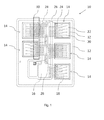
- FIG 1 an embodiment of a power semiconductor module 10 according to the invention is schematically shown. It is obvious for one skilled in the art that a plurality of modules 10 shown in figure 1 may be combined to a power semiconductor arrangement.
- the module 10 according to the invention is particularly suitable for high-voltage applications, or high current applications, respectively.
- the power semiconductor module 10 comprises a substrate 12, on which substrate 12 a plurality of metallizations are formed, these metallizations in turn forming circuit paths. Further, at least one power semiconductor device 14 is located on a metallization 15. Preferably, a plurality of power semiconductor devices 14 is located on a substrate 12, such as 4-5 power semiconductor devices 14. According to figure 2 , five power semiconductor devices 14 are provided.
- the power semiconductor devices 14 are electrically connected to a circuit path 16 via at least one bond wire 18, according to figure 1 by a plurality of bond wires 18. At least one bond wire 18 comprises at least two bond wire feet 20 for attaching the bond wire 18 to a contact 22 of the power semiconductor device 14.
- the bond layout is realized by using stitch bonds and thus at least two bond wire feet 20 on the contact 22, or chip, respectively, per wire 18.
- the bond wire feet 20 of different bond wires 18 which are located closest to the termination 32 of the power semiconductor device 14 being directed towards the circuit path 16, and thus the first bond wire feet 20a of respective power semiconductor devices 14, are highlighted by box 30. It can however be seen that the ends of the bond wires 18 are distributed on the whole bond pad, or contact 22, respectively. It can further be seen that the semiconductor devices 14 are electrically connected via a metallization 24 by bond wires 26 to a control circuit 28.
- bonding layout of bonding wires 18 and the bond wire feet 20 on the contact 22 may be indicated in figure 1 and is described in more detail in the subsequent figures.
- a first bond wire foot 20a is located at a distance d 2 to the termination 32, and that the distance d 2 between the termination 32 and the first bond wire foot 20a, and thus the distance between the respective outer points of the termination 32 and the bond wire foot 20a, lies in the range of d 2 ⁇ 1,5d 1 to d 2 ⁇ 6d 1 , d 1 being the diameter of the bond wire 18. Further, it may be provided that at least one bond wire 20 has a diameter d 1 in the range of ⁇ 300 ⁇ m to ⁇ 500 ⁇ m.
- the minimum distance d 3 between the edge 21 of the contact 22 being directed towards the circuit path 16 and the bond wire 18 in a perpendicular direction of the edge 21 of the contact 22 lies in the range of ⁇ (voltage used/3KV) * 1 mm to ⁇ 3mm + (voltage used/3KV) * 1 mm.
- ⁇ voltage used/3KV
- the bond wire 18 proceeds from the first bond wire foot 20a in a direction towards the circuit path 16 with an angle ⁇ with respect to the upper surface 23 of the contact 22 of equal or more than 50°. Additionally, the bond wire 18 may proceed from the circuit path 16 in the direction to the semiconductor device 14 in an angle ⁇ referring to the upper surface 17 of the circuit path 16 lying in the range ⁇ ⁇ ⁇ . For typical bond layouts this may enhance to reach a small distance between the first bond wire foot 20a and the termination 32 with an easy manufacturing process and further good thermal management. This can additionally avoid a small insulation distance which can lead to loss of voltage blocking capability.
- the bond wire 18 is hereby advantageous to start bonding the bond wire 18 on the chip, or on the contact 22, respectively, and end the bond wire 18 on the substrate 12, or the circuit path 16, respectively, where the bond wire 18 can be cut without risk of chip damage.
- the achievable loop shape of the bond wire 18 may depend on the wiring direction.
- the above bond layout has significant advantages with respect to thermal management and thus with security as well as reliability.
- FIG 3 an embodiment of a bond layout is shown in detail.
- at least one power semiconductor device 14 is electrically connected to a circuit path 16 via two or more bond wires 18, wherein the distance d 4 between two first bond wire feet 20a of adjacent bond wires 18 lies in a range of ⁇ 2mm. This is especially advantageous for current equilibration between the respective bond wire feet 20a and thus between the respective bond wires 18.
- at least one power semiconductor device 14 is electrically connected to a circuit path 16 via two or more bond wires 18, wherein at least two bond wires 18 are provided having a different length.
- the bond layout according to figure 3 further shows that at least one power semiconductor device 14 is electrically connected to a circuit path 16 via two or more bond wires 18, wherein between two first bond wire feet 20a of adjacent bond wires 18 is a distance d 4 and wherein between at least two subsequent adjacent bond wire feet 20b having the same priority is distance d 5 , wherein d 5 ⁇ 2d 4 and further that at least one bond wire 18 at least partly does not proceed parallel to at least one further bond wire 18.
- FIG 4 a further embodiment of a bond layout is shown.
- essentially the same features may be provided according to figure 3 with a comparable bond layout. It is thus referred to the respective description of figure 3 .
- the last bond wire feet 20c are arranged in a distance d 6 from the termination 32 being located opposite to the circuit path 16, which distance d 6 is as well chosen in small dimensions.
- the dimension d 6 may be chosen in the same range as described above with respect to the dimension d 2 . According to this, again the heat influence acting on these bond wire feet 20c is significantly reduced allowing the advantages as described above with respect to choosing the distance d 2 may be provided.
Landscapes
- Wire Bonding (AREA)
Priority Applications (1)
| Application Number | Priority Date | Filing Date | Title |
|---|---|---|---|
| EP20130166986 EP2802007A1 (fr) | 2013-05-08 | 2013-05-08 | Module de puissance à semi-conducteur |
Applications Claiming Priority (1)
| Application Number | Priority Date | Filing Date | Title |
|---|---|---|---|
| EP20130166986 EP2802007A1 (fr) | 2013-05-08 | 2013-05-08 | Module de puissance à semi-conducteur |
Publications (1)
| Publication Number | Publication Date |
|---|---|
| EP2802007A1 true EP2802007A1 (fr) | 2014-11-12 |
Family
ID=48227086
Family Applications (1)
| Application Number | Title | Priority Date | Filing Date |
|---|---|---|---|
| EP20130166986 Withdrawn EP2802007A1 (fr) | 2013-05-08 | 2013-05-08 | Module de puissance à semi-conducteur |
Country Status (1)
| Country | Link |
|---|---|
| EP (1) | EP2802007A1 (fr) |
Cited By (2)
| Publication number | Priority date | Publication date | Assignee | Title |
|---|---|---|---|---|
| WO2016142372A1 (fr) * | 2015-03-12 | 2016-09-15 | Infineon Technologies Bipolar Gmbh & Co. Kg | Module de semi-conducteur de puissance pourvu d'une structure de connexion par soudage améliorée |
| CN106024745A (zh) * | 2016-07-01 | 2016-10-12 | 长电科技(宿迁)有限公司 | 一种半导体管脚贴装结构及其焊接方法 |
Citations (5)
| Publication number | Priority date | Publication date | Assignee | Title |
|---|---|---|---|---|
| JP2004140072A (ja) * | 2002-10-16 | 2004-05-13 | Fuji Electric Device Technology Co Ltd | パワー半導体装置のワイヤボンディング方法 |
| US20040217488A1 (en) * | 2003-05-02 | 2004-11-04 | Luechinger Christoph B. | Ribbon bonding |
| JP2006066704A (ja) * | 2004-08-27 | 2006-03-09 | Toyota Motor Corp | 半導体装置 |
| DE102005039940B4 (de) | 2005-08-24 | 2009-07-02 | Semikron Elektronik Gmbh & Co. Kg | Leistungshalbleitermodul mit Bondverbindung der Leistungshalbleiterbauelemente |
| EP2159834A1 (fr) | 2009-09-01 | 2010-03-03 | ABB Technology AG | Revêtement de fil de connexion conducteur |
-
2013
- 2013-05-08 EP EP20130166986 patent/EP2802007A1/fr not_active Withdrawn
Patent Citations (5)
| Publication number | Priority date | Publication date | Assignee | Title |
|---|---|---|---|---|
| JP2004140072A (ja) * | 2002-10-16 | 2004-05-13 | Fuji Electric Device Technology Co Ltd | パワー半導体装置のワイヤボンディング方法 |
| US20040217488A1 (en) * | 2003-05-02 | 2004-11-04 | Luechinger Christoph B. | Ribbon bonding |
| JP2006066704A (ja) * | 2004-08-27 | 2006-03-09 | Toyota Motor Corp | 半導体装置 |
| DE102005039940B4 (de) | 2005-08-24 | 2009-07-02 | Semikron Elektronik Gmbh & Co. Kg | Leistungshalbleitermodul mit Bondverbindung der Leistungshalbleiterbauelemente |
| EP2159834A1 (fr) | 2009-09-01 | 2010-03-03 | ABB Technology AG | Revêtement de fil de connexion conducteur |
Cited By (6)
| Publication number | Priority date | Publication date | Assignee | Title |
|---|---|---|---|---|
| WO2016142372A1 (fr) * | 2015-03-12 | 2016-09-15 | Infineon Technologies Bipolar Gmbh & Co. Kg | Module de semi-conducteur de puissance pourvu d'une structure de connexion par soudage améliorée |
| CN107210281A (zh) * | 2015-03-12 | 2017-09-26 | 英飞凌科技有限两合公司 | 带有改进的键合连接结构的功率半导体模块 |
| EP3268989A1 (fr) * | 2015-03-12 | 2018-01-17 | Infineon Technologies Bipolar GmbH & Co. KG | Module de semi-conducteur de puissance pourvu d'une structure de connexion par soudage améliorée |
| RU2676190C1 (ru) * | 2015-03-12 | 2018-12-26 | Инфинеон Текнолоджиз Биполар Гмбх Унд Ко. Кг | Силовой полупроводниковый модуль с улучшенной структурой контактных соединителей для приваривания |
| CN107210281B (zh) * | 2015-03-12 | 2020-01-31 | 英飞凌科技有限两合公司 | 带有改进的键合连接结构的功率半导体模块 |
| CN106024745A (zh) * | 2016-07-01 | 2016-10-12 | 长电科技(宿迁)有限公司 | 一种半导体管脚贴装结构及其焊接方法 |
Similar Documents
| Publication | Publication Date | Title |
|---|---|---|
| JP7419781B2 (ja) | 半導体モジュール | |
| US8324726B2 (en) | Semiconductor device, electrode member and electrode member fabrication method | |
| US9171773B2 (en) | Semiconductor device | |
| US10242961B2 (en) | Semiconductor device | |
| US9159715B2 (en) | Miniaturized semiconductor device | |
| US10361136B2 (en) | Semiconductor device and semiconductor module provided with same | |
| US10217690B2 (en) | Semiconductor module that have multiple paths for heat dissipation | |
| JP5605095B2 (ja) | 半導体装置 | |
| US10128345B2 (en) | Semiconductor device | |
| CN103021979A (zh) | 半导体装置 | |
| EP2498289A2 (fr) | Boîtier pour un semi-conducteur à alimentation IGBT doté d'une attache conductrice d'électricité. | |
| CN103928408B (zh) | 功率半导体模块和用于制造功率半导体模块的方法 | |
| EP2571053A1 (fr) | Assemblage semi-conducteur de puissance et son procédé de fabrication | |
| KR101734712B1 (ko) | 파워모듈 | |
| US20170194296A1 (en) | Semiconductor module | |
| EP2178117A1 (fr) | Module d'alimentation semi-conducteur doté d'un refroidissement à double face | |
| US20170170150A1 (en) | Semiconductor module and semiconductor device | |
| EP2802007A1 (fr) | Module de puissance à semi-conducteur | |
| KR20120073302A (ko) | 회로 장치 및 그의 제조 방법 | |
| KR102296270B1 (ko) | 양면 냉각 파워 모듈 및 이의 제조방법 | |
| JP4706551B2 (ja) | パワー半導体素子及びパワーモジュール | |
| CN218996706U (zh) | 一种铜带键合的环氧塑封车用功率模块封装结构 | |
| JP7612545B2 (ja) | 半導体装置 | |
| CN107210281B (zh) | 带有改进的键合连接结构的功率半导体模块 | |
| CN111584422B (zh) | 半导体装置及其制造方法 |
Legal Events
| Date | Code | Title | Description |
|---|---|---|---|
| PUAI | Public reference made under article 153(3) epc to a published international application that has entered the european phase |
Free format text: ORIGINAL CODE: 0009012 |
|
| 17P | Request for examination filed |
Effective date: 20130508 |
|
| AK | Designated contracting states |
Kind code of ref document: A1 Designated state(s): AL AT BE BG CH CY CZ DE DK EE ES FI FR GB GR HR HU IE IS IT LI LT LU LV MC MK MT NL NO PL PT RO RS SE SI SK SM TR |
|
| AX | Request for extension of the european patent |
Extension state: BA ME |
|
| STAA | Information on the status of an ep patent application or granted ep patent |
Free format text: STATUS: THE APPLICATION IS DEEMED TO BE WITHDRAWN |
|
| 18D | Application deemed to be withdrawn |
Effective date: 20150513 |