EP2802137B1 - Verfahren und Vorrichtung zur Bilderzeugung und Verfahren zur Herstellung von gedruckten Produkten - Google Patents
Verfahren und Vorrichtung zur Bilderzeugung und Verfahren zur Herstellung von gedruckten Produkten Download PDFInfo
- Publication number
- EP2802137B1 EP2802137B1 EP14167390.5A EP14167390A EP2802137B1 EP 2802137 B1 EP2802137 B1 EP 2802137B1 EP 14167390 A EP14167390 A EP 14167390A EP 2802137 B1 EP2802137 B1 EP 2802137B1
- Authority
- EP
- European Patent Office
- Prior art keywords
- light
- image data
- region
- edge
- unit
- Prior art date
- Legal status (The legal status is an assumption and is not a legal conclusion. Google has not performed a legal analysis and makes no representation as to the accuracy of the status listed.)
- Active
Links
- 238000000034 method Methods 0.000 title claims description 14
- 238000004519 manufacturing process Methods 0.000 title description 2
- 230000003287 optical effect Effects 0.000 description 69
- 238000010586 diagram Methods 0.000 description 46
- 238000012545 processing Methods 0.000 description 42
- 238000012546 transfer Methods 0.000 description 27
- 230000004048 modification Effects 0.000 description 25
- 238000012986 modification Methods 0.000 description 25
- 238000006243 chemical reaction Methods 0.000 description 24
- 230000008878 coupling Effects 0.000 description 13
- 238000010168 coupling process Methods 0.000 description 13
- 238000005859 coupling reaction Methods 0.000 description 13
- 230000006870 function Effects 0.000 description 8
- 238000007600 charging Methods 0.000 description 7
- 238000004140 cleaning Methods 0.000 description 7
- 230000005684 electric field Effects 0.000 description 7
- 239000003086 colorant Substances 0.000 description 6
- 238000001514 detection method Methods 0.000 description 6
- 230000015654 memory Effects 0.000 description 5
- 238000004891 communication Methods 0.000 description 4
- 238000012937 correction Methods 0.000 description 3
- 230000007423 decrease Effects 0.000 description 3
- 238000007639 printing Methods 0.000 description 3
- 238000009499 grossing Methods 0.000 description 2
- 238000009877 rendering Methods 0.000 description 2
- 230000003936 working memory Effects 0.000 description 2
- 238000004458 analytical method Methods 0.000 description 1
- 230000008859 change Effects 0.000 description 1
- 239000011248 coating agent Substances 0.000 description 1
- 238000000576 coating method Methods 0.000 description 1
- 238000010276 construction Methods 0.000 description 1
- 238000009792 diffusion process Methods 0.000 description 1
- 238000007786 electrostatic charging Methods 0.000 description 1
- 238000005516 engineering process Methods 0.000 description 1
- 238000010191 image analysis Methods 0.000 description 1
- 230000007246 mechanism Effects 0.000 description 1
- 238000009966 trimming Methods 0.000 description 1
- 238000011144 upstream manufacturing Methods 0.000 description 1
Images






Classifications
-
- G—PHYSICS
- G03—PHOTOGRAPHY; CINEMATOGRAPHY; ANALOGOUS TECHNIQUES USING WAVES OTHER THAN OPTICAL WAVES; ELECTROGRAPHY; HOLOGRAPHY
- G03G—ELECTROGRAPHY; ELECTROPHOTOGRAPHY; MAGNETOGRAPHY
- G03G15/00—Apparatus for electrographic processes using a charge pattern
- G03G15/04—Apparatus for electrographic processes using a charge pattern for exposing, i.e. imagewise exposure by optically projecting the original image on a photoconductive recording material
- G03G15/04027—Apparatus for electrographic processes using a charge pattern for exposing, i.e. imagewise exposure by optically projecting the original image on a photoconductive recording material and forming half-tone image
-
- H—ELECTRICITY
- H04—ELECTRIC COMMUNICATION TECHNIQUE
- H04N—PICTORIAL COMMUNICATION, e.g. TELEVISION
- H04N1/00—Scanning, transmission or reproduction of documents or the like, e.g. facsimile transmission; Details thereof
- H04N1/40—Picture signal circuits
- H04N1/40025—Circuits exciting or modulating particular heads for reproducing continuous tone value scales
- H04N1/40037—Circuits exciting or modulating particular heads for reproducing continuous tone value scales the reproducing element being a laser
-
- H—ELECTRICITY
- H04—ELECTRIC COMMUNICATION TECHNIQUE
- H04N—PICTORIAL COMMUNICATION, e.g. TELEVISION
- H04N1/00—Scanning, transmission or reproduction of documents or the like, e.g. facsimile transmission; Details thereof
- H04N1/40—Picture signal circuits
- H04N1/405—Halftoning, i.e. converting the picture signal of a continuous-tone original into a corresponding signal showing only two levels
- H04N1/4055—Halftoning, i.e. converting the picture signal of a continuous-tone original into a corresponding signal showing only two levels producing a clustered dots or a size modulated halftone pattern
- H04N1/4058—Halftoning, i.e. converting the picture signal of a continuous-tone original into a corresponding signal showing only two levels producing a clustered dots or a size modulated halftone pattern with details for producing a halftone screen at an oblique angle
-
- H—ELECTRICITY
- H04—ELECTRIC COMMUNICATION TECHNIQUE
- H04N—PICTORIAL COMMUNICATION, e.g. TELEVISION
- H04N1/00—Scanning, transmission or reproduction of documents or the like, e.g. facsimile transmission; Details thereof
- H04N1/40—Picture signal circuits
- H04N1/409—Edge or detail enhancement; Noise or error suppression
- H04N1/4092—Edge or detail enhancement
Definitions
- the present invention relates generally to methods and apparatuses for forming images, and methods for producing printed products.
- Digital electrophotographic printers have come into wide use in the field of production printing in recent years. Accordingly, there is a demand for an increase in image quality and reliability of digital electrophotographic printers. In particular, there is a strong demand that digital printers be increased in uniformity of gray levels.
- a digital electrophotographic printer typically includes an image processing unit which performs image processing on image data to correct and thereby increase image quality.
- An image processing unit may perform image processing on multi-bit image data of high resolution of 1,200 dots per inch (dpi) or 2,400 dpi, for example.
- Such a digital electrophotographic printer typically includes: a photosensitive drum of which photosensitive surface functions as a surface to be scanned; a light source which emits laser light; a polygon mirror which deflects the laser light emitted from the light source; and a scanning optical system which causes the laser light deflected by the polygon mirror to impinge on the surface (the surface to be scanned) of the photosensitive drum.
- the digital electrophotographic printer may form an electrostatic latent image representing image data on the photosensitive drum by modulating a light beam emitted from the light source according to the image data, illuminating the surface to be scanned with the light beam from the light source, and scanning the light beam across the surface to be scanned.
- a digital electrophotographic printer configured as described above typically employs a device, such as a laser diode array (LDA) or a vertical-cavity surface-emitting laser (VCSEL), having a plurality of light emitters as the light source. Employment of such a device allows the digital electrophotographic printer to form an electrostatic latent image of a resolution of, for example, 2,400 dpi or 4,800 dpi, higher than that of 1,200-dpi image data.
- a device such as a laser diode array (LDA) or a vertical-cavity surface-emitting laser (VCSEL), having a plurality of light emitters as the light source.
- LDA laser diode array
- VCSEL vertical-cavity surface-emitting laser
- an image processing unit of a digital printer applies, as digital half-toning, parallel-line dithering which replaces each uniform-gray-level region (put another way, region of a same pixel value) of image data with a parallel-line pattern.
- Each width of lines constituting the parallel-line pattern varies depending on the pixel value, so that each gray level is expressed as an area percentage.
- Japanese Laid-open Patent Application No. 2004-282344 discloses a technique, in which an image processing unit suppresses image noise without changing screen ruling by generating a binary parallel-line pattern by digital half-toning, increasing resolution of the parallel-line pattern, and thereafter performing interpolation and smoothing.
- Japanese Patent No. 4026271 discloses a technique which increases image quality by increasing resolution by dividing pixels of an image into subpixels, and smoothing edge portions of the image.
- an electrostatic latent image of the pattern formed on a photosensitive drum can have a region where electric field intensity is weak due to an influence exerted from an adjacent line or the like. This is undesirable because, in such a region, toner sticks to the photosensitive drum less reliably.
- Edges of lines of a parallel-line pattern representing low-resolution image data have a shape (stepped profile) assuming a large-step staircase. For this reason, when a highly-dense parallel-line pattern of low-resolution image data is formed on a photosensitive drum, a weak electric-field region can be produced particularly at a stepped profile portion where lines of the pattern are close to each other. In the weak electric-field region, toner can undesirably unevenly stick to the photosensitive drum or be scattered between the lines. Accordingly, it has been difficult for digital printers to form an image of uniform gray levels from low-resolution image data to which parallel-line dithering is applied.
- US 2012/0120454 discloses an image forming apparatus in accordance with the preamble of claim 1.
- the present invention provides an image forming apparatus and method as defined by the appended claims.
- FIG. 1 is a diagram of a schematic configuration of a color printer 2000 according to an embodiment of the present invention.
- the color printer 2000 produces a printed product by transferring toner onto a sheet of recording paper (medium) (hereinafter, "recording sheet").
- the color printer 2000 is a tandem full-color printer which forms a full-color image by overlaying four colors (black, cyan, magenta, and yellow) on one another.
- the color printer 2000 includes an optical scanning device 2010, four photosensitive drum 2030a, 2030b, 2030c, and 2030d (these four are collectively referred to as “photosensitive drums 2030"), four cleaning units 2031a, 2031b, 2031c, and 2031d (these four are collectively referred to as “cleaning units 2031”), and four electrostatic charging devices 2032a, 2032b, 2032c, and 2032d (these four are collectively referred to as "charging devices 2032").
- the color printer 2000 further includes four developing rollers 2033a, 2033b, 2033c, and 2033d (these four are collectively referred to as “developing rollers 2033"), and four toner cartridges 2034a, 2034b, 2034c, and 2034d (these four are collectively referred to as “toner cartridges 2034").
- the color printer 2000 further includes a transfer belt 2040, a transfer roller 2042, a fixing roller 2050, a sheet feeding roller 2054, a pair of registration rollers 2056, a sheet output roller 2058, a sheet feeding tray 2060, a sheet output tray 2070, a communication control device 2080, a density detector 2245, four home-position sensors 2246a, 2246b, 2246c, and 2246d (these four are collectively referred to as "home-position sensors 2246”), and a printer control device 2090.
- the communication control device 2080 controls mutual communication with a host apparatus (e.g., a computer) over a network or the like.
- a host apparatus e.g., a computer
- the printer control device 2090 provides overall control of units included in the color printer 2000.
- the printer control device 2090 includes a central processing unit (CPU), a read only memory (ROM) in which a program described in codes for execution by the CPU and various types of data for use in execution of the program are stored, a random access memory (RAM) which is a working memory, and an analog-to-digital (A/D) converter circuit for converting analog data to digital data.
- the printer control device 2090 controls each of the units according to a request from the host apparatus and transmits image data fed from the host apparatus to the optical scanning device 2010.
- the photosensitive drum 2030a, the charging device 2032a, the developing roller 2033a, the toner cartridge 2034a, and the cleaning unit 2031a are used as a set. These units make up an image forming station (hereinafter, sometimes referred to as "K station") which forms black images.
- K station image forming station
- the photosensitive drum 2030b, the charging device 2032b, the developing roller 2033b, the toner cartridge 2034b, and the cleaning unit 2031b are used as a set. These units make up an image forming station (hereinafter, sometimes referred to as "C station") which forms cyan images.
- C station image forming station
- the photosensitive drum 2030c, the charging device 2032c, the developing roller 2033c, the toner cartridge 2034c, and the cleaning unit 2031c are used as a set. These units make up an image forming station (hereinafter, sometimes referred to as "M station") which forms magenta images.
- M station image forming station
- the photosensitive drum 2030d, the charging device 2032d, the developing roller 2033d, the toner cartridge 2034d, and the cleaning unit 2031d are used as a set. These units make up an image forming station (hereinafter, sometimes referred to as "Y station") which forms yellow images.
- Y station image forming station
- Each of the photosensitive drums 2030 is an example of a latent-image carrier and has a photosensitive layer on its surface.
- the surface of each of the photosensitive drums 2030 functions as a surface to be scanned.
- the photosensitive drums 2030a, 2030b, 2030c, and 2030d are arranged with their rotating axes parallel to each other and rotate in a same direction (e.g., the direction indicated by arrowed lines in FIG. 1 ).
- rotating axes of the photosensitive drums 2030 are parallel to the Y-axis of an XYZ three-dimensional Cartesian coordinate system, in which the photosensitive drums 2030 are arranged in the X-axis direction.
- Each of the charging devices 2032 uniformly electrostatically charges the surface of the corresponding photosensitive drum 2030.
- the optical scanning device 2010 emits light beams which are respectively modulated according to image data (black image data, cyan image data, magenta image data, and yellow image data) on a per-color basis onto the charged surfaces of the photosensitive drums 2030. Charges on the surface of the corresponding photosensitive drum 2030 are dissipated only at places exposed to light. As a result, a latent image representing the image data is formed on the surface of each of the photosensitive drums 2030. The thus-formed latent images move toward the developing rollers 2033 as the photosensitive drums 2030 rotate.
- the configuration of the optical scanning device 2010 will be described in detail later.
- An area, into which image data is to be written, on each of the photosensitive drums 2030 is generally referred to as, for example, "effective scanning area”, “image forming area”, or "effective image area”.
- the toner cartridge 2034a contains black toner.
- the black toner is supplied to the developing roller 2033a.
- the toner cartridge 2034b contains cyan toner.
- the cyan toner is supplied to the developing roller 2033b.
- the toner cartridge 2034c contains magenta toner.
- the magenta toner is supplied to the developing roller 2033c.
- the toner cartridge 2034d contains yellow toner. The yellow toner is supplied to the developing roller 2033d.
- a thin and uniform coating of toner supplied from the corresponding toner cartridge 2034 is applied to the surface of each of the developing rollers 2033 as the developing roller 2033 rotates.
- the toner on the surface of each of the developing rollers 2033 contacts the surface of the corresponding photosensitive drum 2030, the toner transfers only to the illuminated places on the surface and sticks thereto.
- each of the developing rollers 2033 develops the latent image formed on the corresponding photosensitive drum 2030 by causing the toner to stick to the latent image.
- the transfer belt 2040 which is looped over a belt conveying mechanism, is rotated in a fixed direction. An outer surface of the transfer belt 2040 is brought into contact with the surfaces of the photosensitive drums 2030a, 2030b, 2030c, and 2030d, respectively, at locations on the side opposite from the optical scanning device 2010. The outer surface of the transfer belt 2040 is also brought into contact with the transfer roller 2042.
- An image (toner image) formed with toner sticking to the surface of each of the photosensitive drums 2030 moves toward the transfer belt 2040 as the photosensitive drum 2030 rotates.
- the yellow, magenta, cyan, and black toner images are sequentially transferred onto the transfer belt 2040 at respective predetermined timing, and overlaid on one another to form a full-color image.
- the full-color image formed on the transfer belt 2040 moves toward the transfer roller 2042 as the transfer belt 2040 rotates.
- Sheets of recording paper are stored in the sheet feeding tray 2060.
- the sheet feeding roller 2054 is arranged near the sheet feeding tray 2060.
- the sheet feeding roller 2054 picks up the recording sheets one sheet by one sheet from the sheet feeding tray 2060 and conveys the recording sheet to the pair of registration rollers 2056.
- the pair of registration rollers 2056 delivers the recording sheet toward a nip between the transfer belt 2040 and the transfer roller 2042 at predetermined timing. Hence, the full-color image on the transfer belt 2040 is transferred onto the recording sheet.
- the recording sheet, onto which the full-color image is transferred, is delivered to the fixing roller 2050.
- the fixing roller 2050 applies heat and pressure onto the recording sheet.
- the fixing roller 2050 thereby fixes the toner onto the recording sheet.
- Recording sheets, to each of which toner is fixed, are delivered one sheet by one sheet to the sheet output tray 2070 via the sheet output roller 2058 to be stacked on the sheet output tray 2070.
- Each of the cleaning units 2031 removes toner (residual toner) remaining on the surface of the corresponding photosensitive drum 2030.
- the surface of the photosensitive drum 2030, from which the residual toner is removed, returns to a position where the surface faces the corresponding charging device 2032.
- the density detector 2245 is arranged on the negative side of the X-axis (hereinafter, "-X side") (the side upstream from the fixing roller 2050 in a moving direction of the transfer belt 2040 and downstream of the four photosensitive drums 2030) with respect to the transfer belt 2040.
- the density detector 2245 may include, for example, three optical sensors 2245a, 2245b, and 2245c as illustrated in FIG. 2 .
- the optical sensor 2245a is arranged at a position at which the optical sensor 2245a faces a portion (which is at one end in the width direction of the transfer belt 2040) near an end on the -Y side of the effective image area on the transfer belt 2040.
- the optical sensor 2245c is arranged at a position at which the optical sensor 2245c faces a portion (which is at the other end in the width direction of the transfer belt 2040) near an end on the +Y side of the effective image area on the transfer belt 2040.
- the optical sensor 2245b is arranged at about a midpoint position (which is at a width center of the transfer belt 2040) in the main-scanning direction between the optical sensor 2245a and the optical sensor 2245c.
- the center of the optical sensor 2245a in the main-scanning direction i.e., the Y-axis direction
- Y1 the center of the optical sensor 2245a in the main-scanning direction
- Y2 the center of the optical sensor 2245b
- Y3 the center of the optical sensor 2245c
- Each of the optical sensors 2245a, 2245b, and 2245c includes, for example, a light-emitting diode (LED) 11 for emitting light (hereinafter, “detection light”) toward the transfer belt 2040, a specularly-reflected-light photo-detector 12 for receiving light emitted from the LED 11 and then specularly reflected from the transfer belt 2040 or a toner pad on the transfer belt 2040, and a diffusely-reflected-light photo-detector 13 for receiving light emitted from the LED 11 and then diffusely reflected from the transfer belt 2040 or the toner pad on the transfer belt 2040 as illustrated in FIG. 3 .
- Each of the photodetectors 12 and 13 outputs a signal (photoelectric conversion signal) responsive to the intensity of the received light.
- the home-position sensor 2246a detects a rotational home position of the photosensitive drum 2030a.
- the home-position sensor 2246b detects a rotational home position of the photosensitive drum 2030b.
- the home-position sensor 2246c detects a rotational home position of the photosensitive drum 2030c.
- the home-position sensor 2246d detects a rotational home position of the photosensitive drum 2030d.
- FIG. 4 is a diagram of a configuration of an optical system of the optical scanning device 2010.
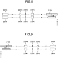
- FIG. 5 is a diagram of an example of an optical path from a light source 2200a to a polygon mirror 2104 and an optical path from a light source 2200b to the polygon mirror 2104.
- FIG. 6 is a diagram of an example of an optical path from a light source 2200c to the polygon mirror 2104 and an optical path from a light source 2200d to the polygon mirror 2104.
- FIG. 7 is a diagram of an example of optical paths from the polygon mirror 2104 to each of the photosensitive drums 2030.
- the configuration of the optical system of the optical scanning device 2010 is described below.
- the optical scanning device 2010 includes, as the optical system, the four light sources 2200a, 2200b, 2200c, and 2200d, four coupling lenses 2201a, 2201b, 2201c, and 2201d, four aperture plates 2202a, 2202b, 2202c, and 2202d, and four cylindrical lenses 2204a, 2204b, 2204c, and 2204d.
- the optical scanning device 2010 further includes, as the optical system, the polygon mirror 2104, four scanning lenses 2105a, 2105b, 2105c, and 2105d, and six folding mirrors 2106a, 2106b, 2106c, 2106d, 2108b, and 2108c. These elements are assembled to predetermined positions in an optical housing.
- the optical scanning device 2010 further includes an electrical system circuit, which will be described later with reference to FIG. 8 and other following figures.
- Each of the light sources 2200a, 2200b, 2200c, and 2200d includes a surface-emitting laser array, in which a plurality of light emitters is arranged in a two-dimensional array.
- the plurality of light emitters of the surface-emitting laser array is arranged in such a manner that when all the light emitters are orthogonally projected onto a virtual line extending in the sub-scanning direction, the light emitters are equidistant from each other.
- Each of the light sources 2200a, 2200b, 2200c, and 2200d may be a vertical-cavity surface-emitting laser (VCSEL), for example.
- VCSEL vertical-cavity surface-emitting laser
- the coupling lens 2201a which is arranged on the optical path of light emitted from the light source 2200a, shapes a light beam passing therethrough into a substantially parallel light beam.
- the coupling lens 2201b which is arranged on the optical path of light emitted from the light source 2200b, shapes a light beam passing therethrough into a substantially parallel light beam.
- the coupling lens 2201c which is arranged on the optical path of light emitted from the light source 2200c, shapes a light beam passing therethrough into a substantially parallel light beam.
- the coupling lens 2201d which is arranged on the optical path of light emitted from the light source 2200d, shapes a light beam passing therethrough into a substantially parallel light beam.
- the aperture plate 2202a has an opening which limits the size of the light beam passing therethrough after exiting from the coupling lens 2201a.
- the aperture plate 2202b has an opening which limits the size of the light beam passing therethrough after exiting from the coupling lens 2201b.
- the aperture plate 2202c has an opening which limits the size of the light beam passing therethrough after exiting from the coupling lens 2201c.
- the aperture plate 2202d has an opening which limits the size of the light beam passing therethrough after exiting from the coupling lens 2201d.
- the cylindrical lens 2204a focuses the light beam exiting from the opening of the aperture plate 2202a with respect to the Z-axis direction to form an image at a position near a deflection reflection surface of the polygon mirror 2104.
- the cylindrical lens 2204b focuses the light beam exiting from the opening of the aperture plate 2202b with respect to the Z-axis direction to form an image at a position near a deflection reflection surface of the polygon mirror 2104.
- the cylindrical lens 2204c focuses the light beam exiting from the opening of the aperture plate 2202c with respect to the Z-axis direction to form an image at a position near a deflection reflection surface of the polygon mirror 2104.
- the cylindrical lens 2204d focuses the light beam exiting from the opening of the aperture plate 2202d with respect to the Z-axis direction to form an image at a position near a deflection reflection surface of the polygon mirror 2104.
- the optical system made up of the coupling lens 2201a, the aperture plate 2202a, and the cylindrical lens 2204a is a pre-deflector optical system of the K station.
- the optical system made up of the coupling lens 2201b, the aperture plate 2202b, and the cylindrical lens 2204b is a pre-deflector optical system of the C station.
- the optical system made up of the coupling lens 2201c, the aperture plate 2202c, and the cylindrical lens 2204c is a pre-deflector optical system of the M station.
- the optical system made up of the coupling lens 2201d, the aperture plate 2202d, and the cylindrical lens 2204d is a pre-deflector optical system of the Y station.
- the polygon mirror 2104 includes four-facet polygon mirrors, which rotate about an axis parallel to the Z-axis, stacked in two layers. Each of the mirror facets is the deflection reflection surface.
- the four-facet polygon mirror on the first layer is arranged so as to deflect the light beam from the cylindrical lens 2204b and the light beam from the cylindrical lens 2204c.
- the four-facet polygon mirror on the second layer is arranged so as to deflect the light beam from the cylindrical lens 2204a and the light beam from the cylindrical lens 2204d.
- Each of the light beam exiting from the cylindrical lens 2204a and the light beam exiting from the cylindrical lens 2204b is deflected toward the -X side with respect to the polygon mirror 2104.
- Each of the light beam exiting from the cylindrical lens 2204c and the light beam exiting from the cylindrical lens 2204d is deflected toward the +X side with respect to the polygon mirror 2104.
- Each of the scanning lenses 2105a, 2105b, 2105c, and 2105d has optical power which causes a light beam to be focused on vicinity of the corresponding photosensitive drum 2030 and which causes a light spot on the surface of the photosensitive drum 2030 to move in the main-scanning direction with a constant velocity as the polygon mirror 2104 rotates.
- the scanning lens 2105a and the scanning lens 2105b are arranged on the -X side with respect to the polygon mirror 2104.
- the scanning lens 2105c and the scanning lens 2105d are arranged on the +X side with respect to the polygon mirror 2104.
- the scanning lens 2105a and the scanning lens 2105b are stacked in the Z-axis direction.
- the scanning lens 2105b is facing the four-facet polygon mirror on the first layer.
- the scanning lens 2105a is facing the four-facet polygon mirror on the second layer.
- the scanning lens 2105c and the scanning lens 2105d are stacked in the Z-axis direction.
- the scanning lens 2105c is facing the four-facet polygon mirror on the first layer.
- the scanning lens 2105d is facing the four-facet polygon mirror on the second layer.
- the light spot moves in the longitudinal direction of the photosensitive drum 2030a as the polygon mirror 2104 rotates. In other words, the light spot scans over the photosensitive drum 2030a.
- the direction in which the scanning light spot moves is the "main-scanning direction" of the photosensitive drum 2030a.
- the direction in which the photosensitive drum 2030a rotates is the "sub-scanning direction" of the photosensitive drum 2030a.
- the light spot moves in the longitudinal direction of the photosensitive drum 2030b as the polygon mirror 2104 rotates. In other words, the light spot scans over the photosensitive drum 2030b.
- the direction in which the scanning light spot moves is the "main-scanning direction" of the photosensitive drum 2030b.
- the direction in which the photosensitive drum 2030b rotates is the "sub-scanning direction" of the photosensitive drum 2030b.
- the light spot moves in the longitudinal direction of the photosensitive drum 2030c as the polygon mirror 2104 rotates. In other words, the light spot scans over the photosensitive drum 2030c.
- the direction in which the scanning light spot moves is the "main-scanning direction" of the photosensitive drum 2030c.
- the direction in which the photosensitive drum 2030c rotates is the "sub-scanning direction" of the photosensitive drum 2030c.
- the light spot moves in the longitudinal direction of the photosensitive drum 2030d as the polygon mirror 2104 rotates. In other words, the light spot scans over the photosensitive drum 2030d.
- the direction in which the scanning light spot moves is the "main-scanning direction" of the photosensitive drum 2030d.
- the direction in which the photosensitive drum 2030d rotates is the "sub-scanning direction" of the photosensitive drum 2030d.
- the folding mirrors 2106a, 2106b, 2106c, 2106d, 2108b, and 2108c are arranged so that optical paths from the polygon mirror 2104 to the photosensitive drums 2030 are equal to each other in length and that light beams impinge at a same incident angle on equivalent incident positions on the photosensitive drums 2030.
- Each of the optical systems arranged on the optical paths between the polygon mirror 2104 and the photosensitive drums 2030 is often referred to as a scanning optical system.
- the scanning lens 2105a and the folding mirror 2106a make up a scanning optical system of the K station.
- the scanning lens 2105b and the two folding mirrors 2106b and 2108b make up a scanning optical system of the C station.
- the scanning lens 2105c and the two folding mirrors 2106c and 2108c make up a scanning optical system of the M station.
- the scanning lens 2105d and the folding mirror 2106d make up a scanning optical system of the Y station.
- the scanning lens 2105 of each of the scanning optical systems may include a plurality of lenses.
- FIG. 8 is a diagram of a configuration of the electrical system of the optical scanning device 2010.
- the optical scanning device 2010 includes, as elements of the electrical system, an interface unit 3101, an image processing unit 3102, and a drive control unit 3103.
- the interface unit 3101 receives, from the printer control device 2090, image data transferred to the printer control device 2090 from a host apparatus (e.g., a computer).
- the interface unit 3101 passes the received image data to the image processing unit 3102 in the subsequent stage.
- the interface unit 3101 receives RGB 8-bit image data of a resolution of 1,200-dpi and passes the image data to the image processing unit 3102.
- the image processing unit 3102 receives the image data from the interface unit 3101 and converts it into color image data of a format suited for an employed printing method.
- the image processing unit 3102 may convert image data of the RGB system into image data for tandem printing (of the CMYK system).
- the image processing unit 3102 performs not only the data format conversion but also various types of image processing.
- the image processing unit 3102 outputs CMYK 2-bit image data of a resolution of 1,200-dpi.
- the resolution of image data to be output from the image processing unit 3102 is not limited to 1,200 dpi, and can be any resolution.
- the resolution of image data to be output from the image processing unit 3102 is referred to as a first resolution hereinafter.
- the drive control unit 3103 receives the image data of the first resolution from the image processing unit 3102 and converts it into color image data of a second resolution suited to driving the light sources. Note that the second resolution is higher than the first resolution. In this example, the drive control unit 3103 converts image data into CMYK 1-bit image data of a resolution of 4,800-dpi.
- the drive control unit 3103 generates a modulated signal for each of the colors by modulating the image data with clock signal which defines light emission timing of the light source 2200.
- the drive control unit 3103 drives each of the light sources 2200a, 2200b, 2200c, and 2200d according to the modulated signal of the corresponding color, thereby causing the light source 2200 to emit light.
- the drive control unit 3103 may be, for example, a one-chip integrated circuit (IC) arranged near the light sources 2200a, 2200b, 2200c, and 2200d.
- the image processing unit 3102 and the interface unit 3101 are arranged away from the light sources 2200a, 2200b, 2200c, and 2200d than the drive control unit 3103.
- a cable 3104 connects between the image processing unit 3102 and the drive control unit 3103.
- the optical scanning device 2010 configured as described above is capable of forming latent images by causing the light sources 2200a, 2200b, 2200c, and 2200d to emit light in accordance with image data.
- FIG. 9 is a diagram of a configuration of the interface unit 3101.
- the interface unit 3101 may include, for example, a flash memory 3211, a RAM 3212, an I/F circuit 3213, and a CPU 3214.
- the flash memory 3211, the RAM 3212, the I/F circuit 3213, and the CPU 3214 are connected to each other via a bus.
- the flash memory 3211 stores a program to be executed by the CPU 3214 and various types of data necessary for the CPU 3214 to execute the program.
- the RAM 3212 is a working memory for use by the CPU 3214 in execution of the program.
- the I/F circuit 3213 carries out mutual communication with the printer control device 2090.
- the CPU 3214 provides overall control of the optical scanning device 2010 by operating according to the program stored in the flash memory 3211.
- the interface unit 3101 configured as described above receives image data (in this example, RGB, 8-bit, 1,200-dpi image data) from the printer control device 2090 and passes the image data to the image processing unit 3102.
- FIG. 10 is a diagram of a configuration of the image processing unit 3102.
- the image processing unit 3102 includes a color conversion unit 3221, a gray component replacement unit (hereinafter, "GCR unit”) 3222, a gamma correction unit 3223, and a digital half-toning unit 3224.
- GCR unit gray component replacement unit
- the color conversion unit 3221 converts 8-bit RGB image data into 8-bit CMY image data.
- the GCR unit 3222 generates a gray (black) component based on the CMY image data, which is generated by the color conversion unit 3221, to thereby generate CMYK image data.
- the gamma correction unit 3223 linearly changes levels of the respective colors using a table or the like.
- the digital half-toning unit 3224 receives 8-bit image data (input image data) from the gamma correction unit 3223.
- the digital half-toning unit 3224 reduces the number of gray levels of the received (input) 8-bit image data and outputs 2-bit image data.
- the digital half-toning unit 3224 may reduce the number of gray levels of the input 8-bit image data by, for example, digital half-toning using a dithering technique or an error diffusion technique.
- the image processing unit 3102 configured as described above outputs CMYK 2-bit image data of the first resolution (e.g., 1,200 dpi) to the drive control unit 3103.
- CMYK 2-bit image data of the first resolution e.g., 1,200 dpi
- a part of or the entire image processing unit 3102 may be implemented in hardware or in a software program executed by a CPU.
- FIG. 11 is a diagram of an example of a parallel-line pattern generated by the digital half-toning unit 3224.
- the digital half-toning unit 3224 performs parallel-line dithering as one of half-toning schemes for reducing the number of gray levels. More specifically, the digital half-toning unit 3224 converts each uniform-pixel-value region in the input 8-bit image data to a parallel-line pattern formed with a plurality of parallel lines extending obliquely with respect to the direction in which pixels are arrayed, thereby expressing each gray level as an area percentage.
- the digital half-toning unit 3224 converts each uniform-pixel-value region, which is a region of pixels having a same pixel value, to a parallel-line pattern formed with a plurality of lines of which area percentage depends on the pixel value. By performing conversion in this manner, the digital half-toning unit 3224 can generate image data, in which each gray level of original (input) image regions is expressed as an area percentage.
- the digital half-toning unit 3224 may generate a parallel-line pattern formed with a predetermined number of lines (screen ruling) per unit length. In this case, the digital half-toning unit 3224 varies the line width of each of the parallel-line pattern according to a pixel value of the original image data. More specifically, the digital half-toning unit 3224 sets the line widths so that the smaller the pixel value, the narrower the line width, and vice versa. By setting the line widths in this manner, the digital half-toning unit 3224 can generate the plurality of lines of which area percentage depends on the corresponding pixel value.
- the digital half-toning unit 3224 may change the screen ruling according to a set value.
- the digital half-toning unit 3224 sets an angle (screen angle) relative to the direction, in which pixels are arrayed, of the plurality of lines constituting the parallel-line pattern according to the set value.
- the digital half-toning unit 3224 may form a parallel-line pattern by rendering a plurality of lines with two gray levels, for example.
- the digital half-toning unit 3224 may assign a black value (i.e., a value which sets the intensity of light to be emitted from the light source 2200 to 100%) to pixels belonging to any line and a white value (i.e., a value which sets the intensity of light to be emitted from the light source 2200 to 0%) to pixels not belonging to any line, for example.
- the digital half-toning unit 3224 may form a parallel-line pattern by rendering a plurality of lines with three or more gray levels, for example.
- the digital half-toning unit 3224 may assign the black value (i.e., the value which sets the intensity of light to be emitted from the light source 2200 to 100%) to pixels belonging to a center portion of any line, a midtone value (i.e., a value which sets the intensity of light to be emitted from the light source 2200 to 50%, for example) to pixels belonging to an edge portion of any line, and the white value (i.e., the value which sets the intensity of light to be emitted from the light source 2200 to 0%) to pixels not belonging to any line, for example.
- the black value i.e., the value which sets the intensity of light to be emitted from the light source 2200 to 100%
- a midtone value i.e., a value which sets the intensity of light to be emitted from the light source 2200 to 50%, for
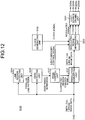
- FIG. 12 is a diagram of a configuration of the drive control unit 3103.
- the drive control unit 3103 includes a resolution converting unit 3231, a clock generating unit 3232, a modulated-signal generating unit 3233, a light-source driving unit 3234, a line-region detecting unit 3235, an edge detecting unit 3236, and an edge control unit 3237.
- the resolution converting unit 3231 receives image data of the first resolution from the image processing unit 3102 and converts it into color image data of the second resolution, which is higher than the first resolution.
- the resolution converting unit 3231 converts CMYK, 2-bit, 1,200-dpi image data into CMYK, 1-bit, 4,800-dpi image data. More specifically, for example, the resolution converting unit 3231 performs resolution conversion by converting each horizontal dot (in the main-scanning direction) in the 1,200-dpi image data represented in 2-bit gray scale into horizontal 4 dots in 4,800-dpi image data represented in 1-bit gray scale.
- the resolution converting unit 3231 converts image data of a resolution N (N is a natural number) into image data of a resolution of m ⁇ N (m is a natural number greater than one).
- the clock generating unit 3232 generates the clock signal which defines light emission timing of the light source 2200.
- the clock signal allows phase modulation at a resolution of, for example, a 1/8 clock period.
- the modulated-signal generating unit 3233 generates a modulated signal for each of the colors by modulating image data of each color with the clock signal.
- the modulated-signal generating unit 3233 generates a modulated signal for each of cyan (C), magenta (M), yellow (Y), and black (K).
- the modulated-signal generating unit 3233 modulates, on the per-color basis, the image data with the clock signal in a manner of synchronizing the image data with write-start timing which depends on the rotational position of the photosensitive drum 2030.
- the modulated-signal generating unit 3233 supplies the modulated signals of the respective colors to the light-source driving unit 3234.
- the light-source driving unit 3234 drives each of the light sources 2200a, 2200b, 2200c, and 2200d in accordance with corresponding one of the modulated signals of the respective colors fed from the modulated-signal generating unit 3233.
- the light-source driving unit 3234 can cause each of the light sources 2200a, 2200b, 2200c, and 2200d to emit light with light intensity according to the modulated signal.
- the line-region detecting unit 3235 receives the image data of the first resolution from the image processing unit 3102 and detects parallel-line patterns from the image data of the first resolution.
- the line-region detecting unit 3235 outputs signals indicating the parallel-line patterns of the image data of the first resolution and detection positions where the patterns are detected.
- the line-region detecting unit 3235 may detect the parallel-line patterns by performing image pattern analysis.
- the line-region detecting unit 3235 may detect the parallel-line patterns by receiving information indicating regions to which the parallel-line dithering is applied from the image processing unit 3102, for example.
- the edge detecting unit 3236 receives the image data of the first resolution from the image processing unit 3102, and the signals indicating the parallel-line patterns and the detection positions from the line-region detecting unit 3235.
- the edge detecting unit 3236 detects pixels (line neighborhoods), each of which is near an edge of any one of the plurality of lines, from the parallel-line patterns of the image data of the first resolution.
- the edge detecting unit 3236 then outputs signals indicating locations of the edge neighborhoods.
- a line neighborhood denotes a portion formed with pixels on a longitudinal side of a line and pixels within a predetermined range from the longitudinal side.
- the edge detecting unit 3236 may detect the edge neighborhoods from the parallel-line patterns of the image data of the first resolution detected by the line-region detecting unit 3235 by pattern matching, for example. Alternatively, the edge detecting unit 3236 may detect the edge neighborhoods by performing image analysis of the regions, which are detected as the parallel-line patterns by the line-region detecting unit 3235.
- the edge control unit 3237 receives the signals indicating the locations of the edge neighborhoods from the edge detecting unit 3236.
- the edge control unit 3237 narrows a region, which is to be illuminated by the light emitted from the light source 2200, in each of the edge neighborhoods of the plurality of lines constituting the parallel-line patterns, while increasing the intensity of the light to be emitted from the light source 2200.
- the edge control unit 3237 controls the resolution conversion performed on the edge neighborhood by supplying an illuminated-region control signal to the resolution converting unit 3231, thereby causing the to-be-illuminated region to be illuminated by the light emitted from the light source 2200 of the edge neighborhood to be narrowed.
- the edge control unit 3237 causes the to-be-illuminated region of the edge neighborhood to be narrowed when the resolution conversion of increasing the resolution of the edge neighborhood from the first resolution (1,200 dpi) to the second resolution (4,800 dpi) is performed.
- the edge control unit 3237 narrows the to-be-illuminated region of the edge neighborhood from an outer side toward a center of the line. In other words, the edge control unit 3237 narrows the to-be-illuminated region by trimming away an outer-edge portion of the line.
- the edge control unit 3237 controls modulation processing performed on the edge neighborhood by supplying a light-intensity control signal to the modulated-signal generating unit 3233, thereby causing the intensity of the light to be emitted to the edge neighborhood from the light source 2200 to increase.
- the edge control unit 3237 controls modulation so that the intensity of light incident on the edge neighborhood becomes higher than the intensity of light incident on the other portion.
- the edge control unit 3237 narrows the to-be-illuminated region and increases the light intensity in a manner of causing the light source 2200 to emit the same luminous energy as luminous energy to be emitted when the edge control unit 3237 controls none of the to-be-illuminated region and the light intensity. More specifically, for example, when halving the to-be-illuminated region, the edge control unit 3237 doubles the light intensity. That is, the edge control unit 3237 narrows the to-be-illuminated region and increases the light intensity so that a product of a ratio of the to-be-illuminated region decrease and a ratio of the light intensity increase is constantly one.
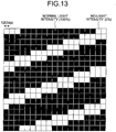
- FIG. 13 is a diagram of a portion of a parallel-line pattern of 1,200-dpi image data. Note that positions of cells in FIGS. 13 to 20 , 22 , and 24 , each illustrating image data, correspond to positions of pixels at the resolution specified in each drawing.
- a plurality of lines constituting a parallel-line pattern extends obliquely with respect to the direction in which pixels are arrayed. Accordingly, as shown in FIG. 13 , each of edges of the lines has a step-like shape of which step height is equal to or larger than one pixel of the first resolution (1,200 dpi).
- a pixel value which causes the light source 2200 to emit light at normal light intensity (100%) is assigned to (black) pixels constituting the lines.
- a pixel value which sets the light source 2200 to no-light intensity (0%) is assigned to (white) pixels not constituting any line.
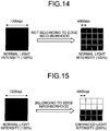
- FIG. 14 is a diagram illustrating resolution conversion performed on a pixel not belonging to any edge neighborhood.
- the resolution converting unit 3231 converts each pixel of the 1,200-dpi image data to 16 pixels (4 horizontal pixels by 4 vertical pixels) of the 4,800-dpi image data.
- the resolution converting unit 3231 assigns a value representing the normal light intensity (100%) to corresponding 16 pixels of the 4,800-dpi image data. By performing conversion in this manner, the resolution converting unit 3231 can keep the light intensity invariant before and after the resolution conversion.
- FIG. 15 is a diagram illustrating resolution conversion performed on a pixel in an edge neighborhood.
- the edge control unit 3237 causes some of the corresponding 16 pixels of 4,800-dpi image data to emit light at enhanced light intensity (200%), which is higher than the normal light intensity, and lights off the remainder of the 16 pixels.
- the edge control unit 3237 can narrow the to-be-illuminated region in the edge neighborhood of each of the lines constituting the parallel-line pattern while increasing the light intensity.
- the edge control unit 3237 may cause 8 pixels of 16 pixels of 4,800-dpi image data to emit light at the enhanced light intensity, and light off the other 8 pixels.
- the edge control unit 3237 can halve the to-be-illuminated region of the edge neighborhood while doubling the light intensity.
- the edge control unit 3237 can narrow the to-be-illuminated region and increase the light intensity in a manner of causing the light source 2200 to emit the same luminous energy as luminous energy to be emitted when the edge control unit 3237 controls none of the to-be-illuminated region and the light intensity.
- the edge control unit 3237 causes the 8 pixels near the center of the line of the 16 pixels of the 4,800-dpi image data to emit light, and lights off the other 8 pixels near the edge of the line. By performing control in this manner, the edge control unit 3237 can narrow the to-be-illuminated region from an outer side toward the center of the line.
- FIG. 16 is a diagram of a portion of a parallel-line pattern of 4,800-dpi image data obtained by increasing the resolution of and performing the edge processing on the parallel-line pattern illustrated in FIG. 13 .
- the edge control unit 3237 narrows a to-be-illuminated region of an edge neighborhood, and causes the edge neighborhood to emit light at the enhanced light intensity higher than the normal light intensity when the resolution conversion of increasing the resolution of a parallel-line pattern from the first resolution (1,200 dpi) to the second resolution (4,800 dpi) is performed.
- the drive control unit 3103 can cause electric field intensity to increase or decrease sharply at an edge portion of an electrostatic latent image formed on the photosensitive drum 2030. If the electric field intensity of the edge portion increases or decreases sharply, no weak electric-field region, to which toner sticks less reliably, will be produced. By making a boundary between a portion, to which toner is to stick, and a portion, to which toner is not to stick, of each of the lines on the electrostatic latent image clear and distinct in this manner, the drive control unit 3103 prevents such an undesirable condition that toner sticks unevenly or that toner is scattered between the lines. As a result, the color printer 2000 can print parallel-line patterns with uniform gray levels.
- a first modification of the embodiment is described below.
- the first modification is substantially similar in function and configuration to the embodiment described above with reference to FIGS. 1 to 16 . Accordingly, like reference symbols designate elements identical or corresponding in function and configuration to those in FIGS. 1 to 16 , for which reason repeated description is omitted below.
- FIG. 17 is a diagram of a portion of a parallel-line pattern of 1,200-dpi image data represented with three levels of light intensity.
- the digital half-toning unit 3224 according to the first modification forms a parallel-line pattern with pixels of three gray levels.
- the digital half-toning unit 3224 forms such a parallel-line pattern as that illustrated FIG. 17 of the first resolution (1,200 dpi) with three gray levels which are the no-light intensity (0%), intermediate light intensity (50%), and the normal light intensity (100%).
- the lines are formed with pixels (black in FIG. 17 ) which cause the light source 2200 to emit light at the normal light intensity (100%) and pixels (crosshatched in FIG. 17 ) which cause the light source 2200 to emit light at the intermediate light intensity (50%). Gaps between the lines are filled with pixels (white in FIG. 17 ) which set the light source 2200 to the no-light intensity (0%).
- FIG. 18 is a diagram illustrating resolution conversion performed on pixels not belonging to any edge neighborhood in image data represented with the three levels of light intensity.
- the resolution converting unit 3231 assigns a value representing the normal light intensity (100%) to corresponding 16 pixels of 4,800-dpi image data.
- the resolution converting unit 3231 causes two vertical center rows (8 pixels) of corresponding 16 pixels of 4,800-dpi image data to emit light at the normal light intensity (100%), and lights off the remainder (8 pixels of vertical rows on the outer sides) of the 16 pixels.
- the resolution converting unit 3231 can keep the light intensity invariant before and after the resolution conversion.
- FIG. 19 is a diagram illustrating resolution conversion performed on pixels in an edge neighborhood in image data represented with the three levels of light intensity.
- the edge control unit 3237 converts these two pixels together at a time as illustrated in FIG. 19 .
- the edge control unit 3237 causes some of corresponding 32 pixels of 4,800-dpi image data to emit light at the enhanced light intensity (200%), and lights off the remainder of the 32 pixels.
- the edge control unit 3237 may cause 12 pixels, which are on the side of the center of the line, of the 32 pixels of the 4,800-dpi image data to emit light at the enhanced light intensity (200%), and sets the other 20 pixels to the no-light intensity (0%).
- the edge control unit 3237 can narrow the to-be-illuminated region and increase the light intensity in a manner of causing the light source 2200 to emit the same luminous energy as luminous energy to be emitted when the edge control unit 3237 controls none of the to-be-illuminated region and the light intensity, also in a case where the parallel-line pattern is represented with three levels of light intensity.
- a second modification of the embodiment is described below.
- the second modification is substantially similar in function and configuration to the embodiment described above with reference to FIGS. 1 to 16 . Accordingly, like reference symbols designate elements identical or corresponding in function and configuration to those in FIGS. 1 to 16 , for which reason repeated description is omitted below.
- FIG. 21 is a diagram of a configuration of the drive control unit 3103 according to the second modification of the embodiment.
- the drive control unit 3103 according to the second modification does not include the resolution converting unit 3231.
- the modulated-signal generating unit 3233 according to the second modification receives, for example, CMYK, 1-bit, 1,200-dpi image data from the image processing unit 3102.
- the edge control unit 3237 supplies an illuminated-region control signal to the modulated-signal generating unit 3233, thereby narrowing a to-be-illuminated region in an edge neighborhood. More specifically, the edge control unit 3237 narrows the to-be-illuminated region by setting a light-on period of pixels in the edge neighborhood shorter than a light-on period of pixels in other region. For example, the edge control unit 3237 may narrow a to-be-illuminated region while increasing the light intensity by doubling the light intensity of pixels in an edge neighborhood and halving a light-on period of the pixels.
- FIG. 22 is a diagram of a portion of a parallel-line pattern of 1,200-dpi image data to be fed to the drive control unit 3103 according to the second modification.
- the drive control unit 3103 receives such 1,200-dpi image data as that illustrated in FIG. 22 represented with pixel values of two gray levels, which are the normal light intensity (100%) and the no-light intensity (0%), from the image processing unit 3102.
- FIG. 23 is a diagram of a portion of a parallel-line pattern of 4,800-dpi image data obtained by the drive control unit 3103 according to the second modification by performing edge processing on the parallel-line pattern illustrated in FIG. 22 .
- the edge control unit 3237 sets the light intensity of pixels in edge neighborhoods of lines to the enhanced light intensity (200%) while halves the light-on period of the pixels (i.e., setting a duty ratio to 50%). By performing control in this manner, the edge control unit 3237 can narrow a to-be-illuminated range of the pixels in the edge neighborhoods in the main-scanning direction.
- the drive control unit 3103 according to the second modification configured as described above can narrow the to-be-illuminated range by controlling the light-on period of the light source 2200. Accordingly, the second modification allows narrowing the to-be-illuminated range while increasing the resolution in the main-scanning direction without using the resolution converting unit 3231.
- a third modification of the embodiment is described below.
- the third modification is substantially similar in function and configuration to the embodiment described above with reference to FIGS. 1 to 16 . Accordingly, like reference symbols designate elements identical or corresponding in function and configuration to those in FIGS. 1 to 16 , for which reason repeated description is omitted below.
- FIG. 24 is a diagram of a configuration of the drive control unit 3103 according to the third modification of the embodiment.
- the line-region detecting unit 3235 according to the third modification receives not only image data but also object information from the image processing unit 3102.
- the object information specifies, on a per-region basis (e.g., on a per-pixel basis) of the image data, a type of an object represented by pixel(s) in the region.
- object information indicates a "text" attribute.
- object information indicates a "graphic shape” attribute.
- object information indicates a "photo" attribute.
- the line-region detecting unit 3235 detects parallel-line patterns based on the object information fed from the image processing unit 3102. For instance, the line-region detecting unit 3235 performs parallel-line pattern detection on a region, of which attribute is "photo” according to the object information and therefore to which parallel-line dithering can be applied. By contrast, the line-region detecting unit 3235 does not perform parallel-line pattern detection on a region, of which attribute is "text" or "graphic shape” according to the object information and therefore to which parallel-line dithering will never be applied. By performing detection in this manner, the line-region detecting unit 3235 can detect parallel-line patterns efficiently and accurately.
- the edge control unit 3237 may detect the number of lines per unit length or a density of the plurality of lines constituting the parallel-line pattern. For example, the edge control unit 3237 may detect the number of lines per unit length or the density of the plurality of lines by pattern matching. Alternatively, the edge control unit 3237 may detect the number of lines per unit length or the density of the plurality of lines by acquiring information about the number of lines per unit length or information about the density of the parallel-line pattern from the image processing unit 3102.
- the edge control unit 3237 may preferably stop changing a to-be-illuminated region and light intensity of an edge neighborhood if the number of lines per unit length or the density is smaller than a preset value.
- the edge control unit 3237 can stop changing the to-be-illuminated region and the light intensity, thereby reducing the amount of operations to be performed.
- an image with a parallel-line pattern can be formed with uniform gray levels.
Landscapes
- Engineering & Computer Science (AREA)
- Multimedia (AREA)
- Signal Processing (AREA)
- Physics & Mathematics (AREA)
- Optics & Photonics (AREA)
- General Physics & Mathematics (AREA)
- Laser Beam Printer (AREA)
- Control Or Security For Electrophotography (AREA)
- Facsimile Image Signal Circuits (AREA)
- Color, Gradation (AREA)
- Image Processing (AREA)
Claims (12)
- Bilderzeugungsvorrichtung zum Erzeugen eines Bilds in Übereinstimmung mit Licht, das veranlasst wird, von einer Lichtquelle (2200) emittiert zu werden, wobei die Bilderzeugungsvorrichtung Folgendes umfasst:eine Lichtquelle (2200);eine digitale Halbtonrastereinheit (3224), die konfiguriert ist, einen Bereich für einen einheitlichen Pixelwert, der mit Pixeln mit einem gleichen Pixelwert von Bilddaten gebildet wird, in ein Muster paralleler Linien, das mit einer Vielzahl von parallelen Linien gebildet wird, umzuwandeln, wobei die Pixel in einem rechteckigen Array mit einer ersten Achse und einer zweiten Achse angeordnet sind, wobei die erste Achse orthogonal zur zweiten Achse ist, wobei die Vielzahl von parallelen Linien sich in Bezug auf die erste Achse und die zweite Achse schräg erstreckt, wodurch jeder Grauwert der Bilddaten als ein Flächenprozentsatz ausgedrückt wird;eine Erzeugungseinheit für ein moduliertes Signal (3233), die konfiguriert ist, ein moduliertes Signal durch Modulieren der Bilddaten, bei denen jeder Grauwert als ein Flächenprozentsatz ausgedrückt wird, mit einem Taktsignal zu erzeugen; undeine Lichtquellenantriebseinheit (3234), die konfiguriert ist, die Lichtquelle gemäß dem modulierten Signal anzutreiben;gekennzeichnet durch:eine Kantensteuereinheit, die konfiguriert ist, ein Steuersignal für einen beleuchteten Bereich und ein Steuersignal für eine Lichtintensität zu erzeugen,die Kantensteuereinheit, die konfiguriert ist, einen zu beleuchtenden Bereich zu verengen, wobei der zu beleuchtende Bereich ein Bereich ist, der durch von der Lichtquelle emittiertes Licht beleuchtet werden soll, in jedem von Kantennahbereichen der Vielzahl von Linien, die das Muster paralleler Linien bilden, unddie Kantensteuereinheit, die auch konfiguriert ist, die Intensität des zu den Kantennahbereichen emittierten Lichts zu erhöhen, um höher als die Intensität von Licht, das auf einen anderen Abschnitt einfällt, zu werden.
- Bilderzeugungsvorrichtung nach Anspruch 1, wobei die digitale Halbtonrastereinheit (3224) den Bereich für einen einheitlichen Pixelwert in ein Muster paralleler Linien umwandelt, das mit einer Vielzahl von Linien gebildet ist, deren Flächenprozentsatz von dem Pixelwert abhängt.
- Bilderzeugungsvorrichtung nach Anspruch 1 oder 2, wobei die Kantensteuereinheit (3237) den zu beleuchtenden Bereich verengt und die Lichtintensität auf eine Weise erhöht, bei der die Lichtquelle (2200) veranlasst wird, eine gleiche Lichtenergie wie Lichtenergie, die emittiert werden soll, zu emittieren, wenn die Kantensteuereinheit (3237) keines von dem zu beleuchtenden Bereich und der Lichtintensität steuert.
- Bilderzeugungsvorrichtung nach einem der Ansprüche 1 bis 3, wobei die Kantensteuereinheit (3237) den zu beleuchtenden Bereich von einer Außenseite zu einer Mitte der Linie verengt.
- Bilderzeugungsvorrichtung nach einem der Ansprüche 1 bis 3, wobei die Kantensteuereinheit (3237) den zu beleuchtenden Bereich durch Festlegen einer Lichteinschaltdauer von Pixeln, die zu dem Kantennahbereich gehören, kürzer als eine Lichteinschaltdauer von Pixeln, die zu einem anderen Bereich gehören, verengt.
- Bilderzeugungsvorrichtung nach einem der Ansprüche 1 bis 5, ferner umfassend eine Auflösungsumwandlungseinheit (3231), wobei
die digitale Halbtonrastereinheit (3224) Bilddaten einer ersten Auflösung ausgibt,
die Auflösungsumwandlungseinheit (3231) die Bilddaten der ersten Auflösung in Bilddaten einer zweiten Auflösung umwandelt, wobei die zweite Auflösung höher als die erste Auflösung ist; und
die Kantensteuereinheit (3237) die Lichtquelle auf Grundlage der Bilddaten der zweiten Auflösung steuert. - Bilderzeugungsvorrichtung nach Anspruch 6, ferner umfassend:eine Linienbereicherfassungseinheit (3235), die konfiguriert ist, das Muster paralleler Linien aus den Bilddaten der ersten Auflösung zu erfassen; undeinen Kantenerfassungseinheit (3236), die konfiguriert ist, den Kantennahbereich von jeder der Vielzahl von Linien, die das Muster paralleler Linien bilden, durch Musterabgleich zu erfassen.
- Bilderzeugungsvorrichtung nach Anspruch 7, wobei die Linienbereicherfassungseinheit (3235) für jeden Bereich der Bilddaten der ersten Auflösung Objektinformationen, die einen Typ eines durch Pixel in dem Bereich dargestellten Objekts spezifizieren, erhält und das Muster paralleler Linien auf Grundlage der erhaltenen Objektinformationen erfasst.
- Bilderzeugungsvorrichtung nach einem der Ansprüche 1 bis 8, wobei, wenn eine Anzahl der Vielzahl von Linien pro Einheitslänge oder Dichte der Vielzahl von Linien kleiner als ein voreingestellter Wert ist, die Kantensteuereinheit (3237) ein Ändern des zu beleuchtenden Bereichs und der Lichtintensität in dem Kantennahbereich stoppt.
- Bilderzeugungsvorrichtung nach einem der Ansprüche 1 bis 9, wobei die Lichtquelle (2200) ein oberflächenemittierender Laser mit vertikaler Kavität ist.
- Bilderzeugungsverfahren zum Erzeugen eines Bilds in Übereinstimmung mit von einer Lichtquelle emittiertem Licht, wobei das Bilderzeugungsverfahren Folgendes umfasst:Durchführen von digitalem Halbtonrastern durch Umwandeln eines Bereichs für einen einheitlichen Pixelwert, der mit Pixeln mit einem gleichen Pixelwert von Bilddaten erzeugt wird, in ein Muster paralleler Linien, das mit einer Vielzahl von parallelen Linien erzeugt wird, wobei die Pixel in einem rechteckigen Array mit einer ersten Achse und einer zweiten Achse angeordnet sind, wobei die erste Achse orthogonal zur zweiten Achse ist, wobei die parallelen Linien sich schräg in Bezug auf die erste Achse und die zweite Achse erstrecken, wodurch jeder Grauwert der Bilddaten als ein Flächenprozentsatz ausgedrückt wird;Durchführen von Kantensteuerung durch Erzeugen eines Steuersignals für einen beleuchteten Bereich und eines Steuersignals für eine Lichtintensität,Verengen eines zu beleuchtenden Bereichs, wobei der zu beleuchtende Bereich ein Bereich ist, der durch von der Lichtquelle emittiertes Licht beleuchtet werden soll, in jedem von Kantennahbereichen der Vielzahl von Linien, die das Muster paralleler Linien bilden, undErhöhen der Intensität des zu den Kantennahbereichen emittierten Lichts, um höher als die Intensität von Licht, das von auf einen anderen Abschnitt einfällt, zu werden;Erzeugen eines modulierten Signals durch Modulieren der Bilddaten, bei denen jeder Grauwert als ein Flächenprozentsatz ausgedrückt wird, mit einem Taktsignal; undAntreiben der Lichtquelle gemäß dem modulierten Signal.
- Bilderzeugungsverfahren nach Anspruch 11, ferner umfassend:Erzeugen eines elektrostatischen latenten Bilds auf einem latenten Bildträger mit Licht von der Lichtquelle durch Antreiben der Lichtquelle gemäß dem modulierten Signal;Veranlassen, dass Toner an dem elektrostatischen latenten Bild, das auf dem latenten Bildträger erzeugt wird, festklebt; undÜbertragen des Toners auf ein Medium, wodurch ein Druckprodukt produziert wird.
Applications Claiming Priority (1)
| Application Number | Priority Date | Filing Date | Title |
|---|---|---|---|
| JP2013100139A JP6171547B2 (ja) | 2013-05-10 | 2013-05-10 | 画像形成装置、画像形成方法および印刷物の製造方法 |
Publications (2)
| Publication Number | Publication Date |
|---|---|
| EP2802137A1 EP2802137A1 (de) | 2014-11-12 |
| EP2802137B1 true EP2802137B1 (de) | 2019-07-24 |
Family
ID=50639374
Family Applications (1)
| Application Number | Title | Priority Date | Filing Date |
|---|---|---|---|
| EP14167390.5A Active EP2802137B1 (de) | 2013-05-10 | 2014-05-07 | Verfahren und Vorrichtung zur Bilderzeugung und Verfahren zur Herstellung von gedruckten Produkten |
Country Status (3)
| Country | Link |
|---|---|
| US (1) | US8982422B2 (de) |
| EP (1) | EP2802137B1 (de) |
| JP (1) | JP6171547B2 (de) |
Families Citing this family (22)
| Publication number | Priority date | Publication date | Assignee | Title |
|---|---|---|---|---|
| JP6167654B2 (ja) * | 2013-05-09 | 2017-07-26 | 株式会社リコー | 画像形成装置、画像形成方法および印刷物の製造方法 |
| US9521295B2 (en) | 2013-12-03 | 2016-12-13 | Ricoh Company, Ltd. | Image forming apparatus and image forming method |
| JP6418479B2 (ja) * | 2013-12-25 | 2018-11-07 | 株式会社リコー | 画像形成方法、画像形成装置 |
| JP6425008B2 (ja) | 2014-01-10 | 2018-11-21 | 株式会社リコー | 画像形成装置及び画像形成方法 |
| JP6256125B2 (ja) | 2014-03-13 | 2018-01-10 | 株式会社リコー | 画像形成装置 |
| US9517636B2 (en) * | 2014-05-13 | 2016-12-13 | Ricoh Company, Ltd. | Image forming method, image forming apparatus, and print material production method to form an electrostatic latent image by selective light power exposure |
| JP6364971B2 (ja) | 2014-06-03 | 2018-08-01 | 株式会社リコー | 画像形成装置 |
| JP6332623B2 (ja) * | 2014-06-05 | 2018-05-30 | 株式会社リコー | 画像形成装置及び画像形成方法 |
| JP2016021664A (ja) | 2014-07-14 | 2016-02-04 | 株式会社リコー | 画像形成装置 |
| JP6596814B2 (ja) * | 2014-11-25 | 2019-10-30 | 株式会社リコー | 画像形成装置 |
| JP6492722B2 (ja) * | 2015-02-09 | 2019-04-03 | 株式会社リコー | 光源駆動制御装置、画像形成装置、光源駆動制御方法およびプログラム |
| US9659243B2 (en) | 2015-02-20 | 2017-05-23 | Ricoh Company, Ltd. | Image forming apparatus and method for driving light source |
| JP6524731B2 (ja) | 2015-03-17 | 2019-06-05 | 株式会社リコー | 画像形成装置及び画像形成方法 |
| US9778592B2 (en) * | 2015-05-12 | 2017-10-03 | Ricoh Company, Ltd. | Image forming method and image forming apparatus including a high power exposure pixel group |
| JP2017208669A (ja) | 2016-05-17 | 2017-11-24 | 株式会社リコー | 画像処理装置、駆動制御装置、光源制御装置、画像形成装置、および画像処理方法 |
| JP6673004B2 (ja) | 2016-05-19 | 2020-03-25 | 株式会社リコー | 画像処理装置、駆動制御装置、光源制御装置、画像形成装置、および画像処理方法 |
| JP6673018B2 (ja) | 2016-05-30 | 2020-03-25 | 株式会社リコー | 画像形成装置及び画像形成方法 |
| JP2018056757A (ja) | 2016-09-28 | 2018-04-05 | 株式会社リコー | 画像処理装置、駆動制御装置、光源制御装置、画像形成装置および画像処理方法 |
| CN106546598B (zh) * | 2016-10-28 | 2019-09-24 | 鞍钢未来钢铁研究院有限公司 | 带钢表面检测系统光源自适应控制方法 |
| JP2018136475A (ja) * | 2017-02-23 | 2018-08-30 | ブラザー工業株式会社 | 走査光学装置 |
| JP6953808B2 (ja) | 2017-06-08 | 2021-10-27 | 株式会社リコー | 光源制御装置及び画像形成装置 |
| CN109285521B (zh) * | 2018-11-20 | 2020-09-08 | 惠科股份有限公司 | 像素驱动方法、像素驱动装置和计算机设备 |
Family Cites Families (47)
| Publication number | Priority date | Publication date | Assignee | Title |
|---|---|---|---|---|
| US5973709A (en) | 1992-06-24 | 1999-10-26 | Oki Electric Industry Co., Ltd. | Printer and process for printing different size dots by setting drive energies based on adjacent data bit logic |
| JP4053674B2 (ja) | 1998-12-21 | 2008-02-27 | 株式会社東芝 | 画像形成装置および画像形成方法 |
| JP4026271B2 (ja) * | 1999-03-23 | 2007-12-26 | コニカミノルタビジネステクノロジーズ株式会社 | 画像処理装置 |
| JP2001096794A (ja) * | 1999-09-29 | 2001-04-10 | Fuji Xerox Co Ltd | 走査露光装置、半導体レーザ駆動回路、画像形成装置 |
| JP2002300388A (ja) * | 2001-03-30 | 2002-10-11 | Ricoh Co Ltd | 万線判定装置、像域分離装置、画像処理装置、画像形成装置、プログラム及び記憶媒体 |
| JP2002326389A (ja) * | 2001-04-27 | 2002-11-12 | Ricoh Co Ltd | 画像形成装置 |
| US6791596B2 (en) | 2001-06-28 | 2004-09-14 | Ricoh Company, Ltd. | Method and apparatus for image forming capable of effectively generating pixel clock pulses |
| EP1418749A3 (de) * | 2002-10-16 | 2009-03-18 | FUJIFILM Corporation | Bildaufzeichnungsgerät, sowie Verfahren und Vorrichtung zur Bilderzeugung |
| JP2004282344A (ja) * | 2003-03-14 | 2004-10-07 | Toshiba Tec Corp | 画像処理方法 |
| US7496121B2 (en) | 2003-03-20 | 2009-02-24 | Ricoh Company, Ltd. | Laser modulating and driving device and image reproducing apparatus using the same |
| JP2004354986A (ja) * | 2003-05-02 | 2004-12-16 | Fuji Photo Film Co Ltd | 画像形成方法および装置 |
| JP2005084609A (ja) * | 2003-09-11 | 2005-03-31 | Fuji Photo Film Co Ltd | 画像露光装置における光量調整方法 |
| JP2005096094A (ja) | 2003-09-22 | 2005-04-14 | Ricoh Co Ltd | カラー画像形成装置、半導体レーザ変調駆動装置および画像形成装置 |
| US6949891B2 (en) | 2003-11-28 | 2005-09-27 | Fuji Photo Film Co., Ltd. | Light quantity adjusting method, light quantity adjusting apparatus, and image forming apparatus |
| JP4341908B2 (ja) | 2004-01-07 | 2009-10-14 | 株式会社リコー | 画素クロック及びパルス変調信号生成装置、光走査装置並びに画像形成装置 |
| JP4404351B2 (ja) | 2004-04-12 | 2010-01-27 | 株式会社リコー | 画素クロック生成回路及び画像形成装置 |
| KR100601692B1 (ko) * | 2004-07-14 | 2006-07-14 | 삼성전자주식회사 | 레이저 프린터의 하프톤 처리 방법 및 이에 적합한 장치 |
| US7936493B2 (en) | 2005-06-21 | 2011-05-03 | Ricoh Company, Ltd. | Dot position correcting apparatus, optical scanning apparatus, imaging apparatus, and color imaging apparatus |
| JP2007148346A (ja) | 2005-10-25 | 2007-06-14 | Ricoh Co Ltd | 光走査装置及び画像形成装置 |
| US8253768B2 (en) | 2005-12-09 | 2012-08-28 | Ricoh Company, Ltd. | Optical scanner and image forming apparatus |
| DE102007002211A1 (de) * | 2006-02-06 | 2007-08-09 | Heidelberger Druckmaschinen Ag | Verfahren zur Erzeugung eines Rasterpunktes auf einer Druckform |
| JP2007269001A (ja) | 2006-03-10 | 2007-10-18 | Ricoh Co Ltd | 光走査装置、光走査方法、画像形成装置、カラー画像形成装置、プログラム、記録媒体 |
| JP4912071B2 (ja) | 2006-08-04 | 2012-04-04 | 株式会社リコー | 光走査装置、光走査方法、画像形成装置、カラー画像形成装置、プログラム、記録媒体 |
| WO2008033126A1 (en) * | 2006-09-13 | 2008-03-20 | Hewlett-Packard Development Company, L.P. | Electrographic dot gain and optical density decoupling method, xerographic image reproduction, and systems, methods and software relating thereto |
| JP4863840B2 (ja) | 2006-10-27 | 2012-01-25 | 株式会社リコー | 画素形成装置、光走査装置、光走査方法、画像形成装置、カラー画像形成装置 |
| JP2008153742A (ja) * | 2006-12-14 | 2008-07-03 | Canon Inc | 画像記録装置 |
| JP5083867B2 (ja) | 2007-03-02 | 2012-11-28 | 株式会社リコー | 光源駆動装置、光走査装置及び画像形成装置 |
| US7995251B2 (en) | 2007-03-30 | 2011-08-09 | Ricoh Company, Limited | Optical scanning device, optical scanning method, and image forming apparatus |
| JP4953918B2 (ja) | 2007-05-23 | 2012-06-13 | 株式会社リコー | 光源駆動装置、光走査装置及び画像形成装置 |
| JP5348601B2 (ja) | 2007-05-28 | 2013-11-20 | 株式会社リコー | 光源装置、光走査装置及び画像形成装置 |
| US7675532B2 (en) * | 2007-09-28 | 2010-03-09 | Canon Kabushiki Kaisha | Image-forming apparatus and control method thereof |
| JP4506854B2 (ja) * | 2008-03-04 | 2010-07-21 | 富士ゼロックス株式会社 | 画像処理装置および画像形成装置 |
| JP5036634B2 (ja) | 2008-06-10 | 2012-09-26 | 株式会社リコー | 光源装置、光走査装置及び画像形成装置 |
| US8237760B2 (en) | 2008-08-19 | 2012-08-07 | Ricoh Company, Ltd. | Light-source driving device, optical scanning device, and counting method |
| JP5402072B2 (ja) | 2009-02-23 | 2014-01-29 | 株式会社リコー | 光源駆動装置、光走査装置及び画像形成装置 |
| JP5471569B2 (ja) | 2010-02-18 | 2014-04-16 | 株式会社リコー | レーザ駆動装置、光走査装置、画像形成装置及びレーザ駆動方法 |
| JP2011216843A (ja) | 2010-03-16 | 2011-10-27 | Ricoh Co Ltd | 半導体レーザ駆動装置、及びこれを含む画像形成装置 |
| JP5477087B2 (ja) * | 2010-03-17 | 2014-04-23 | 株式会社リコー | 画像形成装置および画像形成方法 |
| JP2011258796A (ja) | 2010-06-10 | 2011-12-22 | Ricoh Co Ltd | レーザ駆動装置、光走査装置並びに画像形成装置 |
| JP5644230B2 (ja) * | 2010-07-21 | 2014-12-24 | 富士ゼロックス株式会社 | 画像処理装置及び画像処理方法 |
| US8610971B2 (en) | 2010-10-20 | 2013-12-17 | Ricoh Company, Limited | Image forming apparatus |
| JP2012109796A (ja) | 2010-11-17 | 2012-06-07 | Ricoh Co Ltd | 画像処理装置、制御方法及びプログラム |
| JP5679110B2 (ja) | 2011-01-25 | 2015-03-04 | 株式会社リコー | 画像形成装置 |
| JP5853418B2 (ja) | 2011-05-20 | 2016-02-09 | 株式会社リコー | 光源駆動装置及び画像形成装置 |
| US8654168B2 (en) | 2011-08-03 | 2014-02-18 | Ricoh Company, Ltd. | Optical scanning device, image forming apparatus, and optical scanning device designing method |
| US8983318B2 (en) | 2012-03-16 | 2015-03-17 | Ricoh Company, Ltd. | Image forming apparatus with a density sensor for detecting density fluctuations |
| US8929759B2 (en) | 2012-05-10 | 2015-01-06 | Ricoh Company, Limited | Image forming apparatus and density change suppressing method |
-
2013
- 2013-05-10 JP JP2013100139A patent/JP6171547B2/ja not_active Expired - Fee Related
-
2014
- 2014-05-05 US US14/269,332 patent/US8982422B2/en not_active Expired - Fee Related
- 2014-05-07 EP EP14167390.5A patent/EP2802137B1/de active Active
Non-Patent Citations (1)
| Title |
|---|
| None * |
Also Published As
| Publication number | Publication date |
|---|---|
| US8982422B2 (en) | 2015-03-17 |
| JP6171547B2 (ja) | 2017-08-02 |
| US20140333941A1 (en) | 2014-11-13 |
| EP2802137A1 (de) | 2014-11-12 |
| JP2014218049A (ja) | 2014-11-20 |
Similar Documents
| Publication | Publication Date | Title |
|---|---|---|
| EP2802137B1 (de) | Verfahren und Vorrichtung zur Bilderzeugung und Verfahren zur Herstellung von gedruckten Produkten | |
| EP2802138B1 (de) | Bilderzeugungsvorrichtung, Bilderzeugungsverfahren und Verfahren zur Herstellung von Druckmaterial | |
| EP2952967B1 (de) | Bilderzeugungsvorrichtung | |
| EP2799930B1 (de) | Vorrichtung zur Bilderzeugung und Verfahren zur Bilderzeugung | |
| US9760813B2 (en) | Image forming apparatus | |
| US9466016B2 (en) | Image forming apparatus which forms image data indicating whether a pixel is for a character or line | |
| EP3118688B1 (de) | Bilderzeugungsvorrichtung und bilderzeugungsverfahren | |
| US10133971B2 (en) | Image forming apparatus and method for driving light source | |
| JP6492722B2 (ja) | 光源駆動制御装置、画像形成装置、光源駆動制御方法およびプログラム | |
| RU2654395C2 (ru) | Устройство формирования изображений | |
| JP2016064653A (ja) | 画像形成装置 | |
| JP6406414B2 (ja) | 画像形成装置 | |
| JP6852284B2 (ja) | 画像形成装置及び画像形成方法 |
Legal Events
| Date | Code | Title | Description |
|---|---|---|---|
| PUAI | Public reference made under article 153(3) epc to a published international application that has entered the european phase |
Free format text: ORIGINAL CODE: 0009012 |
|
| 17P | Request for examination filed |
Effective date: 20140507 |
|
| AK | Designated contracting states |
Kind code of ref document: A1 Designated state(s): AL AT BE BG CH CY CZ DE DK EE ES FI FR GB GR HR HU IE IS IT LI LT LU LV MC MK MT NL NO PL PT RO RS SE SI SK SM TR |
|
| AX | Request for extension of the european patent |
Extension state: BA ME |
|
| STAA | Information on the status of an ep patent application or granted ep patent |
Free format text: STATUS: EXAMINATION IS IN PROGRESS |
|
| 17Q | First examination report despatched |
Effective date: 20180103 |
|
| GRAP | Despatch of communication of intention to grant a patent |
Free format text: ORIGINAL CODE: EPIDOSNIGR1 |
|
| STAA | Information on the status of an ep patent application or granted ep patent |
Free format text: STATUS: GRANT OF PATENT IS INTENDED |
|
| INTG | Intention to grant announced |
Effective date: 20190304 |
|
| GRAS | Grant fee paid |
Free format text: ORIGINAL CODE: EPIDOSNIGR3 |
|
| GRAA | (expected) grant |
Free format text: ORIGINAL CODE: 0009210 |
|
| STAA | Information on the status of an ep patent application or granted ep patent |
Free format text: STATUS: THE PATENT HAS BEEN GRANTED |
|
| AK | Designated contracting states |
Kind code of ref document: B1 Designated state(s): AL AT BE BG CH CY CZ DE DK EE ES FI FR GB GR HR HU IE IS IT LI LT LU LV MC MK MT NL NO PL PT RO RS SE SI SK SM TR |
|
| REG | Reference to a national code |
Ref country code: GB Ref legal event code: FG4D |
|
| REG | Reference to a national code |
Ref country code: CH Ref legal event code: EP |
|
| REG | Reference to a national code |
Ref country code: DE Ref legal event code: R096 Ref document number: 602014050359 Country of ref document: DE |
|
| REG | Reference to a national code |
Ref country code: AT Ref legal event code: REF Ref document number: 1159664 Country of ref document: AT Kind code of ref document: T Effective date: 20190815 |
|
| REG | Reference to a national code |
Ref country code: IE Ref legal event code: FG4D |
|
| REG | Reference to a national code |
Ref country code: NL Ref legal event code: MP Effective date: 20190724 |
|
| REG | Reference to a national code |
Ref country code: LT Ref legal event code: MG4D |
|
| REG | Reference to a national code |
Ref country code: AT Ref legal event code: MK05 Ref document number: 1159664 Country of ref document: AT Kind code of ref document: T Effective date: 20190724 |
|
| PG25 | Lapsed in a contracting state [announced via postgrant information from national office to epo] |
Ref country code: SE Free format text: LAPSE BECAUSE OF FAILURE TO SUBMIT A TRANSLATION OF THE DESCRIPTION OR TO PAY THE FEE WITHIN THE PRESCRIBED TIME-LIMIT Effective date: 20190724 Ref country code: AT Free format text: LAPSE BECAUSE OF FAILURE TO SUBMIT A TRANSLATION OF THE DESCRIPTION OR TO PAY THE FEE WITHIN THE PRESCRIBED TIME-LIMIT Effective date: 20190724 Ref country code: BG Free format text: LAPSE BECAUSE OF FAILURE TO SUBMIT A TRANSLATION OF THE DESCRIPTION OR TO PAY THE FEE WITHIN THE PRESCRIBED TIME-LIMIT Effective date: 20191024 Ref country code: HR Free format text: LAPSE BECAUSE OF FAILURE TO SUBMIT A TRANSLATION OF THE DESCRIPTION OR TO PAY THE FEE WITHIN THE PRESCRIBED TIME-LIMIT Effective date: 20190724 Ref country code: NO Free format text: LAPSE BECAUSE OF FAILURE TO SUBMIT A TRANSLATION OF THE DESCRIPTION OR TO PAY THE FEE WITHIN THE PRESCRIBED TIME-LIMIT Effective date: 20191024 Ref country code: LT Free format text: LAPSE BECAUSE OF FAILURE TO SUBMIT A TRANSLATION OF THE DESCRIPTION OR TO PAY THE FEE WITHIN THE PRESCRIBED TIME-LIMIT Effective date: 20190724 Ref country code: PT Free format text: LAPSE BECAUSE OF FAILURE TO SUBMIT A TRANSLATION OF THE DESCRIPTION OR TO PAY THE FEE WITHIN THE PRESCRIBED TIME-LIMIT Effective date: 20191125 Ref country code: NL Free format text: LAPSE BECAUSE OF FAILURE TO SUBMIT A TRANSLATION OF THE DESCRIPTION OR TO PAY THE FEE WITHIN THE PRESCRIBED TIME-LIMIT Effective date: 20190724 Ref country code: FI Free format text: LAPSE BECAUSE OF FAILURE TO SUBMIT A TRANSLATION OF THE DESCRIPTION OR TO PAY THE FEE WITHIN THE PRESCRIBED TIME-LIMIT Effective date: 20190724 |
|
| PG25 | Lapsed in a contracting state [announced via postgrant information from national office to epo] |
Ref country code: LV Free format text: LAPSE BECAUSE OF FAILURE TO SUBMIT A TRANSLATION OF THE DESCRIPTION OR TO PAY THE FEE WITHIN THE PRESCRIBED TIME-LIMIT Effective date: 20190724 Ref country code: RS Free format text: LAPSE BECAUSE OF FAILURE TO SUBMIT A TRANSLATION OF THE DESCRIPTION OR TO PAY THE FEE WITHIN THE PRESCRIBED TIME-LIMIT Effective date: 20190724 Ref country code: GR Free format text: LAPSE BECAUSE OF FAILURE TO SUBMIT A TRANSLATION OF THE DESCRIPTION OR TO PAY THE FEE WITHIN THE PRESCRIBED TIME-LIMIT Effective date: 20191025 Ref country code: ES Free format text: LAPSE BECAUSE OF FAILURE TO SUBMIT A TRANSLATION OF THE DESCRIPTION OR TO PAY THE FEE WITHIN THE PRESCRIBED TIME-LIMIT Effective date: 20190724 Ref country code: IS Free format text: LAPSE BECAUSE OF FAILURE TO SUBMIT A TRANSLATION OF THE DESCRIPTION OR TO PAY THE FEE WITHIN THE PRESCRIBED TIME-LIMIT Effective date: 20191124 Ref country code: AL Free format text: LAPSE BECAUSE OF FAILURE TO SUBMIT A TRANSLATION OF THE DESCRIPTION OR TO PAY THE FEE WITHIN THE PRESCRIBED TIME-LIMIT Effective date: 20190724 |
|
| PG25 | Lapsed in a contracting state [announced via postgrant information from national office to epo] |
Ref country code: TR Free format text: LAPSE BECAUSE OF FAILURE TO SUBMIT A TRANSLATION OF THE DESCRIPTION OR TO PAY THE FEE WITHIN THE PRESCRIBED TIME-LIMIT Effective date: 20190724 |
|
| PG25 | Lapsed in a contracting state [announced via postgrant information from national office to epo] |
Ref country code: EE Free format text: LAPSE BECAUSE OF FAILURE TO SUBMIT A TRANSLATION OF THE DESCRIPTION OR TO PAY THE FEE WITHIN THE PRESCRIBED TIME-LIMIT Effective date: 20190724 Ref country code: IT Free format text: LAPSE BECAUSE OF FAILURE TO SUBMIT A TRANSLATION OF THE DESCRIPTION OR TO PAY THE FEE WITHIN THE PRESCRIBED TIME-LIMIT Effective date: 20190724 Ref country code: DK Free format text: LAPSE BECAUSE OF FAILURE TO SUBMIT A TRANSLATION OF THE DESCRIPTION OR TO PAY THE FEE WITHIN THE PRESCRIBED TIME-LIMIT Effective date: 20190724 Ref country code: RO Free format text: LAPSE BECAUSE OF FAILURE TO SUBMIT A TRANSLATION OF THE DESCRIPTION OR TO PAY THE FEE WITHIN THE PRESCRIBED TIME-LIMIT Effective date: 20190724 Ref country code: PL Free format text: LAPSE BECAUSE OF FAILURE TO SUBMIT A TRANSLATION OF THE DESCRIPTION OR TO PAY THE FEE WITHIN THE PRESCRIBED TIME-LIMIT Effective date: 20190724 |
|
| PG25 | Lapsed in a contracting state [announced via postgrant information from national office to epo] |
Ref country code: IS Free format text: LAPSE BECAUSE OF FAILURE TO SUBMIT A TRANSLATION OF THE DESCRIPTION OR TO PAY THE FEE WITHIN THE PRESCRIBED TIME-LIMIT Effective date: 20200224 Ref country code: SK Free format text: LAPSE BECAUSE OF FAILURE TO SUBMIT A TRANSLATION OF THE DESCRIPTION OR TO PAY THE FEE WITHIN THE PRESCRIBED TIME-LIMIT Effective date: 20190724 Ref country code: CZ Free format text: LAPSE BECAUSE OF FAILURE TO SUBMIT A TRANSLATION OF THE DESCRIPTION OR TO PAY THE FEE WITHIN THE PRESCRIBED TIME-LIMIT Effective date: 20190724 Ref country code: SM Free format text: LAPSE BECAUSE OF FAILURE TO SUBMIT A TRANSLATION OF THE DESCRIPTION OR TO PAY THE FEE WITHIN THE PRESCRIBED TIME-LIMIT Effective date: 20190724 |
|
| REG | Reference to a national code |
Ref country code: DE Ref legal event code: R097 Ref document number: 602014050359 Country of ref document: DE |
|
| PLBE | No opposition filed within time limit |
Free format text: ORIGINAL CODE: 0009261 |
|
| STAA | Information on the status of an ep patent application or granted ep patent |
Free format text: STATUS: NO OPPOSITION FILED WITHIN TIME LIMIT |
|
| PG2D | Information on lapse in contracting state deleted |
Ref country code: IS |
|
| 26N | No opposition filed |
Effective date: 20200603 |
|
| PG25 | Lapsed in a contracting state [announced via postgrant information from national office to epo] |
Ref country code: SI Free format text: LAPSE BECAUSE OF FAILURE TO SUBMIT A TRANSLATION OF THE DESCRIPTION OR TO PAY THE FEE WITHIN THE PRESCRIBED TIME-LIMIT Effective date: 20190724 |
|
| PG25 | Lapsed in a contracting state [announced via postgrant information from national office to epo] |
Ref country code: LI Free format text: LAPSE BECAUSE OF NON-PAYMENT OF DUE FEES Effective date: 20200531 Ref country code: CH Free format text: LAPSE BECAUSE OF NON-PAYMENT OF DUE FEES Effective date: 20200531 Ref country code: MC Free format text: LAPSE BECAUSE OF FAILURE TO SUBMIT A TRANSLATION OF THE DESCRIPTION OR TO PAY THE FEE WITHIN THE PRESCRIBED TIME-LIMIT Effective date: 20190724 |
|
| REG | Reference to a national code |
Ref country code: BE Ref legal event code: MM Effective date: 20200531 |
|
| PG25 | Lapsed in a contracting state [announced via postgrant information from national office to epo] |
Ref country code: LU Free format text: LAPSE BECAUSE OF NON-PAYMENT OF DUE FEES Effective date: 20200507 |
|
| PG25 | Lapsed in a contracting state [announced via postgrant information from national office to epo] |
Ref country code: IE Free format text: LAPSE BECAUSE OF NON-PAYMENT OF DUE FEES Effective date: 20200507 |
|
| PG25 | Lapsed in a contracting state [announced via postgrant information from national office to epo] |
Ref country code: BE Free format text: LAPSE BECAUSE OF NON-PAYMENT OF DUE FEES Effective date: 20200531 |
|
| PG25 | Lapsed in a contracting state [announced via postgrant information from national office to epo] |
Ref country code: MT Free format text: LAPSE BECAUSE OF FAILURE TO SUBMIT A TRANSLATION OF THE DESCRIPTION OR TO PAY THE FEE WITHIN THE PRESCRIBED TIME-LIMIT Effective date: 20190724 Ref country code: CY Free format text: LAPSE BECAUSE OF FAILURE TO SUBMIT A TRANSLATION OF THE DESCRIPTION OR TO PAY THE FEE WITHIN THE PRESCRIBED TIME-LIMIT Effective date: 20190724 |
|
| PG25 | Lapsed in a contracting state [announced via postgrant information from national office to epo] |
Ref country code: MK Free format text: LAPSE BECAUSE OF FAILURE TO SUBMIT A TRANSLATION OF THE DESCRIPTION OR TO PAY THE FEE WITHIN THE PRESCRIBED TIME-LIMIT Effective date: 20190724 |
|
| PGFP | Annual fee paid to national office [announced via postgrant information from national office to epo] |
Ref country code: GB Payment date: 20220520 Year of fee payment: 9 Ref country code: FR Payment date: 20220523 Year of fee payment: 9 Ref country code: DE Payment date: 20220519 Year of fee payment: 9 |
|
| P01 | Opt-out of the competence of the unified patent court (upc) registered |
Effective date: 20230522 |
|
| REG | Reference to a national code |
Ref country code: DE Ref legal event code: R119 Ref document number: 602014050359 Country of ref document: DE |
|
| GBPC | Gb: european patent ceased through non-payment of renewal fee |
Effective date: 20230507 |
|
| PG25 | Lapsed in a contracting state [announced via postgrant information from national office to epo] |
Ref country code: DE Free format text: LAPSE BECAUSE OF NON-PAYMENT OF DUE FEES Effective date: 20231201 Ref country code: GB Free format text: LAPSE BECAUSE OF NON-PAYMENT OF DUE FEES Effective date: 20230507 |
|
| PG25 | Lapsed in a contracting state [announced via postgrant information from national office to epo] |
Ref country code: FR Free format text: LAPSE BECAUSE OF NON-PAYMENT OF DUE FEES Effective date: 20230531 |