EP2804202A1 - Substrat composite hétérogène oxydé thermiquement et son procédé de fabrication - Google Patents
Substrat composite hétérogène oxydé thermiquement et son procédé de fabrication Download PDFInfo
- Publication number
- EP2804202A1 EP2804202A1 EP20130736379 EP13736379A EP2804202A1 EP 2804202 A1 EP2804202 A1 EP 2804202A1 EP 20130736379 EP20130736379 EP 20130736379 EP 13736379 A EP13736379 A EP 13736379A EP 2804202 A1 EP2804202 A1 EP 2804202A1
- Authority
- EP
- European Patent Office
- Prior art keywords
- heterogeneous composite
- composite substrate
- thermally oxidized
- substrate
- heat treatment
- Prior art date
- Legal status (The legal status is an assumption and is not a legal conclusion. Google has not performed a legal analysis and makes no representation as to the accuracy of the status listed.)
- Granted
Links
Images


Classifications
-
- H—ELECTRICITY
- H10—SEMICONDUCTOR DEVICES; ELECTRIC SOLID-STATE DEVICES NOT OTHERWISE PROVIDED FOR
- H10P—GENERIC PROCESSES OR APPARATUS FOR THE MANUFACTURE OR TREATMENT OF DEVICES COVERED BY CLASS H10
- H10P14/00—Formation of materials, e.g. in the shape of layers or pillars
- H10P14/60—Formation of materials, e.g. in the shape of layers or pillars of insulating materials
- H10P14/63—Formation of materials, e.g. in the shape of layers or pillars of insulating materials characterised by the formation processes
- H10P14/6302—Non-deposition formation processes
- H10P14/6304—Formation by oxidation, e.g. oxidation of the substrate
- H10P14/6306—Formation by oxidation, e.g. oxidation of the substrate of the semiconductor materials
- H10P14/6308—Formation by oxidation, e.g. oxidation of the substrate of the semiconductor materials of Group IV semiconductors
- H10P14/6309—Formation by oxidation, e.g. oxidation of the substrate of the semiconductor materials of Group IV semiconductors of silicon in uncombined form, i.e. pure silicon
-
- H—ELECTRICITY
- H10—SEMICONDUCTOR DEVICES; ELECTRIC SOLID-STATE DEVICES NOT OTHERWISE PROVIDED FOR
- H10D—INORGANIC ELECTRIC SEMICONDUCTOR DEVICES
- H10D30/00—Field-effect transistors [FET]
- H10D30/60—Insulated-gate field-effect transistors [IGFET]
- H10D30/67—Thin-film transistors [TFT]
- H10D30/6758—Thin-film transistors [TFT] characterised by the insulating substrates
-
- H—ELECTRICITY
- H10—SEMICONDUCTOR DEVICES; ELECTRIC SOLID-STATE DEVICES NOT OTHERWISE PROVIDED FOR
- H10D—INORGANIC ELECTRIC SEMICONDUCTOR DEVICES
- H10D62/00—Semiconductor bodies, or regions thereof, of devices having potential barriers
- H10D62/10—Shapes, relative sizes or dispositions of the regions of the semiconductor bodies; Shapes of the semiconductor bodies
- H10D62/113—Isolations within a component, i.e. internal isolations
-
- H—ELECTRICITY
- H10—SEMICONDUCTOR DEVICES; ELECTRIC SOLID-STATE DEVICES NOT OTHERWISE PROVIDED FOR
- H10P—GENERIC PROCESSES OR APPARATUS FOR THE MANUFACTURE OR TREATMENT OF DEVICES COVERED BY CLASS H10
- H10P14/00—Formation of materials, e.g. in the shape of layers or pillars
- H10P14/60—Formation of materials, e.g. in the shape of layers or pillars of insulating materials
- H10P14/63—Formation of materials, e.g. in the shape of layers or pillars of insulating materials characterised by the formation processes
- H10P14/6302—Non-deposition formation processes
- H10P14/6322—Formation by thermal treatments
-
- H—ELECTRICITY
- H10—SEMICONDUCTOR DEVICES; ELECTRIC SOLID-STATE DEVICES NOT OTHERWISE PROVIDED FOR
- H10P—GENERIC PROCESSES OR APPARATUS FOR THE MANUFACTURE OR TREATMENT OF DEVICES COVERED BY CLASS H10
- H10P90/00—Preparation of wafers not covered by a single main group of this subclass, e.g. wafer reinforcement
- H10P90/19—Preparing inhomogeneous wafers
- H10P90/1904—Preparing vertically inhomogeneous wafers
- H10P90/1906—Preparing SOI wafers
-
- H—ELECTRICITY
- H10—SEMICONDUCTOR DEVICES; ELECTRIC SOLID-STATE DEVICES NOT OTHERWISE PROVIDED FOR
- H10P—GENERIC PROCESSES OR APPARATUS FOR THE MANUFACTURE OR TREATMENT OF DEVICES COVERED BY CLASS H10
- H10P90/00—Preparation of wafers not covered by a single main group of this subclass, e.g. wafer reinforcement
- H10P90/19—Preparing inhomogeneous wafers
- H10P90/1904—Preparing vertically inhomogeneous wafers
- H10P90/1906—Preparing SOI wafers
- H10P90/1914—Preparing SOI wafers using bonding
-
- H—ELECTRICITY
- H10—SEMICONDUCTOR DEVICES; ELECTRIC SOLID-STATE DEVICES NOT OTHERWISE PROVIDED FOR
- H10P—GENERIC PROCESSES OR APPARATUS FOR THE MANUFACTURE OR TREATMENT OF DEVICES COVERED BY CLASS H10
- H10P95/00—Generic processes or apparatus for manufacture or treatments not covered by the other groups of this subclass
- H10P95/90—Thermal treatments, e.g. annealing or sintering
-
- H—ELECTRICITY
- H10—SEMICONDUCTOR DEVICES; ELECTRIC SOLID-STATE DEVICES NOT OTHERWISE PROVIDED FOR
- H10W—GENERIC PACKAGES, INTERCONNECTIONS, CONNECTORS OR OTHER CONSTRUCTIONAL DETAILS OF DEVICES COVERED BY CLASS H10
- H10W10/00—Isolation regions in semiconductor bodies between components of integrated devices
- H10W10/10—Isolation regions comprising dielectric materials
- H10W10/181—Semiconductor-on-insulator [SOI] isolation regions, e.g. buried oxide regions of SOI wafers
Definitions
- This invention relates to a thermally oxidized heterogeneous composite substrate obtained from thermal oxidative treatment of a heterogeneous composite substrate comprising a single crystal silicon film formed on a handle substrate of glass, quartz, sapphire or the like, and a method for manufacturing the same.
- Silicon on insulator (SOI) wafers are widely used for the purpose of reducing parasitic capacitance, thereby accelerating device performance. Attractive among SOI wafers are silicon on quartz (SOQ) and silicon on sapphire (SOS) in which the handle wafer is a transparent insulating wafer. SOQ is expected to find use in optoelectronic applications that take advantage of high transparency of quartz, or in high-frequency devices that take advantage of a low dielectric loss of quartz. Since SOS whose handle substrate is made of sapphire has high transparency, a low dielectric loss, and a high thermal conductivity, which is unavailable from quartz, SOS is expected to find use in heat-generating high-frequency devices.
- heterogeneous materials e.g., SOQ, SOS and SOG
- typical device processes involve heat treatment at a high temperature in excess of 850°C to form a gate oxide film.
- heterogeneous composite substrates such high-temperature process applies strong compressive/tensile stresses to the silicon thin film to form various defects such as micro-cracks.
- the cause originating from the heterogeneous composite substrate is a substantial difference in coefficient of expansion between the support substrate known as "handle substrate” and the upper layer or silicon thin film. This is the essential problem of heterogeneous composite substrates.
- An object of the invention which has been made under the above-mentioned circumstances, is to provide a thermally oxidized heterogeneous composite substrate having a minimized number of micro-cracks and other defects left after high-temperature treatment in excess of 850°C to form an oxide layer, and a method for manufacturing the same.
- a transparent insulating wafer (quartz, glass, sapphire or the like) having a silicon thin film transferred thereon is subjected to heat treatment, which may be referred to as previous heat treatment, prior to high-temperature treatment in excess of 850°C, and the temperature of the previous heat treatment ranges from 650°C to 850°C.
- the previous heat treatment is a treatment at 650°C to 850°C for reducing defects which are otherwise formed during high-temperature treatment in excess of 850°C.
- the previous heat treatment is also regarded as a treatment for averaging localized stresses over the entire wafer surface. It is estimated that the localized stresses are caused by material strains and density gradation of the handle substrate, in-plane non-uniformity of the bonding process and the like.
- the previous heat treatment is a treatment for increasing the bond strength at the bonding interface to a sufficient level before the high-temperature treatment temperature is reached, for thereby preventing the silicon thin film from peeling or shifting when strong stresses are applied thereto.
- High-temperature treatment typically oxidative treatment is carried out subsequent to the previous heat treatment, with this sequence being effective for reducing the number of defects left after oxidation.
- the present invention provides a thermally oxidized heterogeneous composite substrate and a method for manufacturing the same, as defined below.
- a thermally oxidized heterogeneous composite substrate having a minimized number of defects after thermal oxidation is available.
- a thermally oxidized heterogeneous composite substrate is obtained by subjecting a heterogeneous composite substrate comprising a single crystal silicon film on a handle substrate to previous heat treatment at 650 to 850°C, and thereafter conducting thermal oxidative treatment at a temperature in excess of 850°C.
- a buried oxide (BOX) layer may intervene between the handle substrate and the single crystal silicon film.
- SOQ obtained by bonding silicon to quartz has a CE difference of 2.04 ppm
- SOS has a CE difference of 4.4 ppm at minimum and 5.1 ppm at maximum. Since the CE of sapphire varies with orientation, a choice of a sapphire substrate having a low CE for reducing the CE difference may further increase the benefits of the invention. Specifically, it is effective to use C-face wafers (7.0 ppm) or R-face wafers ( ⁇ 7.4 ppm) rather than A-face wafers having a high CE.
- the handle substrate has a coefficient of thermal expansion (CTE) of 0.54 to 7.4 ppm at 400°C or lower, and a sapphire wafer has a CE of up to 7.4 ppm at room temperature to 400°C.
- CTE coefficient of thermal expansion
- the handle substrate has a thickness of 500 to 800 ⁇ m, especially 600 to 725 ⁇ m, and the single crystal silicon film has a thickness of 50 to 500 nm, especially 100 to 350 nm.
- the buried oxide (BOX) layer when interposed, preferably has a thickness of 25 to 150 nm. It is noted that the BOX layer may be formed by the same method as disclosed in JP-A 2002-305292 with regard to the formation of BOX layer in SOI wafer.
- previous heat treatment is carried out at a temperature of 650 to 850°C, preferably 700 to 850°C.
- the atmosphere of previous heat treatment is not particularly limited as long as it is easy to handle. Typical of the atmosphere are argon, nitrogen, oxygen, hydrogen, and helium. A mixture of an inert gas such as argon or nitrogen with an oxidizing gas is acceptable.
- the time of previous heat treatment is preferably 0.5 to 6 hours, especially 1 to 3 hours. Too short a time may fail to achieve the object of the invention whereas too long a time may invite a cost increase.
- the previous heat treatment is followed by thermal oxidative treatment.
- the conditions used in the thermal oxidative treatment may be selected from well-known conditions.
- the heat treatment temperature should exceed 850°C, and is preferably from higher than 900°C to 1,000°C, more preferably 950 to 1,000°C, although the heat treatment temperature is not particularly limited as long as an oxide film of the desired thickness is available.
- the previous heat treatment may be at a temperature of 650 to 900°C, especially 700 to 900°C.
- the heat treatment atmosphere is typically dry oxygen or water vapor.
- the heat treatment time is not particularly limited as long as an oxide film of the desired thickness is available.
- a thermally oxidized heterogeneous composite substrate having an outstandingly reduced number of defects is obtained.
- the number of defects in a composite substrate may be determined by a HF immersion test.
- SOQ or SOS is immersed in a HF solution, with which the inside buried oxide (BOX) layer is etched via defects, during which defects are enlarged to a sufficient size to be detectable even under an optical microscope. Easy inspection is possible with this test as long as the BOX layer has a thickness of 25 to 500 nm. If the BOX layer is too thin, HF may not penetrate. If the BOX layer is too thick, HF may penetrate too fast, which is detrimental to inspection.
- SOS wafers including a sapphire wafer (R-face) of 150 mm diameter and 600 ⁇ m thick as the handle substrate.
- the silicon layer had a thickness of 200 nm
- the BOX layer had a thickness of 200 nm.
- the wafers were subjected to previous heat treatment at 600°C, 650°C, 700°C, 800°C, 850°C, and 900°C.
- the atmosphere was argon, and the holding time was 1 hour.
- One more wafer was provided as a reference without previous heat treatment.
- wet oxidation was carried out at 1,000°C to form an oxide film of 200 nm thick.
- the wafers as oxidized were immersed in 10% HF solution for 30 minutes, after which the number of defects was counted, with the results shown in FIG. 1 .
- previous heat treatment was at 650°C to 850°C
- the number of defects was reduced.
- previous heat treatment was at 600°C
- the number of defects was not so reduced, probably because 600°C was an insufficient temperature to gain the desired effect.
- previous heat treatment was at 900°C, defects formed already during the previous heat treatment. The optimum temperature seems to range from 650°C to 850°C.
- SOQ wafers including a quartz wafer of 150 mm diameter and 625 ⁇ m thick as the handle substrate.
- the silicon layer had a thickness of 200 nm
- the BOX layer had a thickness of 200 nm.
- the wafers were subjected to previous heat treatment at 600°C, 650°C, 700°C, 800°C, 850°C, and 900°C.
- the atmosphere was argon, and the holding time was 1 hour.
- One more wafer was provided as a reference without previous heat treatment.
- wet oxidation was carried out at 950°C to form an oxide film of 200 nm thick.
- the wafers as oxidized were immersed in 10% HF solution for 30 minutes, after which the number of defects was counted, with the results shown in FIG. 2 .
- previous heat treatment was at 650°C to 850°C
- the number of defects was reduced.
- previous heat treatment was at 600°C
- the number of defects was not so reduced, probably because 600°C was an insufficient temperature to gain the desired effect.
- previous heat treatment was at 900°C, defects formed already during the previous heat treatment. The optimum temperature seems to range from 650°C to 850°C.
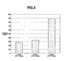
- the silicon layer had a thickness of 200 nm
- the BOX layer had a thickness of 200 nm.
- the wafers were subjected to previous heat treatment at 800°C. The atmosphere was argon, and the holding time was 1 hour. On these wafers, wet oxidation was carried out at 1,000°C to form an oxide film of 200 nm thick.
- the wafers as oxidized were immersed in 10% HF solution for 30 minutes, after which the number of defects was counted, with the results shown in FIG. 3 .
- the number of defects was reduced more effectively than in the case of A-face.
- the inventive method is illustrated with reference to specific examples using quartz and sapphire, the invention is equally effective when materials having an intermediate CTE (0.54 to 7.4 ppm) between quartz and sapphire are used as the handle substrate.
Landscapes
- Formation Of Insulating Films (AREA)
- Crystals, And After-Treatments Of Crystals (AREA)
- Thin Film Transistor (AREA)
Applications Claiming Priority (2)
| Application Number | Priority Date | Filing Date | Title |
|---|---|---|---|
| JP2012003856 | 2012-01-12 | ||
| PCT/JP2013/050387 WO2013105634A1 (fr) | 2012-01-12 | 2013-01-11 | Substrat composite hétérogène oxydé thermiquement et son procédé de fabrication |
Publications (3)
| Publication Number | Publication Date |
|---|---|
| EP2804202A1 true EP2804202A1 (fr) | 2014-11-19 |
| EP2804202A4 EP2804202A4 (fr) | 2015-09-16 |
| EP2804202B1 EP2804202B1 (fr) | 2021-02-24 |
Family
ID=48781576
Family Applications (1)
| Application Number | Title | Priority Date | Filing Date |
|---|---|---|---|
| EP13736379.2A Active EP2804202B1 (fr) | 2012-01-12 | 2013-01-11 | Procédé de fabrication d'un substrat composite hétérogène oxydé thermiquement |
Country Status (8)
| Country | Link |
|---|---|
| US (1) | US10103021B2 (fr) |
| EP (1) | EP2804202B1 (fr) |
| JP (2) | JPWO2013105634A1 (fr) |
| KR (1) | KR102055933B1 (fr) |
| CN (1) | CN104040686B (fr) |
| SG (1) | SG11201404039UA (fr) |
| TW (1) | TWI576474B (fr) |
| WO (1) | WO2013105634A1 (fr) |
Families Citing this family (5)
| Publication number | Priority date | Publication date | Assignee | Title |
|---|---|---|---|---|
| EP2993686B1 (fr) * | 2013-05-01 | 2021-05-26 | Shin-Etsu Chemical Co., Ltd. | Procédé de production de substrat hybride |
| JP6121356B2 (ja) * | 2014-03-31 | 2017-04-26 | 信越化学工業株式会社 | 酸化膜付き異種soi基板の製造方法 |
| JP6121357B2 (ja) * | 2014-03-31 | 2017-04-26 | 信越化学工業株式会社 | 酸化膜付き異種soi基板の欠陥検出方法 |
| JP7262421B2 (ja) * | 2020-05-08 | 2023-04-21 | 信越化学工業株式会社 | 圧電体複合基板およびその製造方法 |
| JP7402112B2 (ja) | 2020-05-08 | 2023-12-20 | 信越化学工業株式会社 | 圧電性単結晶膜を備えた複合基板の製造方法 |
Family Cites Families (33)
| Publication number | Priority date | Publication date | Assignee | Title |
|---|---|---|---|---|
| US4178191A (en) * | 1978-08-10 | 1979-12-11 | Rca Corp. | Process of making a planar MOS silicon-on-insulating substrate device |
| US4509990A (en) * | 1982-11-15 | 1985-04-09 | Hughes Aircraft Company | Solid phase epitaxy and regrowth process with controlled defect density profiling for heteroepitaxial semiconductor on insulator composite substrates |
| JPS59159563A (ja) * | 1983-03-02 | 1984-09-10 | Toshiba Corp | 半導体装置の製造方法 |
| US5395788A (en) * | 1991-03-15 | 1995-03-07 | Shin Etsu Handotai Co., Ltd. | Method of producing semiconductor substrate |
| US6312968B1 (en) * | 1993-06-30 | 2001-11-06 | The United States Of America As Represented By The Secretary Of The Navy | Method for fabricating an electrically addressable silicon-on-sapphire light valve |
| JPH1140682A (ja) * | 1997-07-18 | 1999-02-12 | Sony Corp | 不揮発性半導体記憶装置及びその製造方法 |
| JPH11145438A (ja) * | 1997-11-13 | 1999-05-28 | Shin Etsu Handotai Co Ltd | Soiウエーハの製造方法ならびにこの方法で製造されるsoiウエーハ |
| FR2777115B1 (fr) * | 1998-04-07 | 2001-07-13 | Commissariat Energie Atomique | Procede de traitement de substrats semi-conducteurs et structures obtenues par ce procede |
| JPH11330438A (ja) * | 1998-05-08 | 1999-11-30 | Shin Etsu Handotai Co Ltd | Soiウエーハの製造方法ならびにこの方法で製造されるsoiウエーハ |
| US6417078B1 (en) | 2000-05-03 | 2002-07-09 | Ibis Technology Corporation | Implantation process using sub-stoichiometric, oxygen doses at different energies |
| US6797604B2 (en) | 2000-05-08 | 2004-09-28 | International Business Machines Corporation | Method for manufacturing device substrate with metal back-gate and structure formed thereby |
| JP4304879B2 (ja) | 2001-04-06 | 2009-07-29 | 信越半導体株式会社 | 水素イオンまたは希ガスイオンの注入量の決定方法 |
| US6649535B1 (en) | 2002-02-12 | 2003-11-18 | Taiwan Semiconductor Manufacturing Company | Method for ultra-thin gate oxide growth |
| US7176528B2 (en) | 2003-02-18 | 2007-02-13 | Corning Incorporated | Glass-based SOI structures |
| FR2855909B1 (fr) * | 2003-06-06 | 2005-08-26 | Soitec Silicon On Insulator | Procede d'obtention concomitante d'au moins une paire de structures comprenant au moins une couche utile reportee sur un substrat |
| KR100588647B1 (ko) | 2003-12-30 | 2006-06-12 | 동부일렉트로닉스 주식회사 | 반도체 소자의 제조 방법 |
| JP2005217288A (ja) * | 2004-01-30 | 2005-08-11 | Seiko Epson Corp | 電気光学装置の製造方法 |
| JP4407384B2 (ja) | 2004-05-28 | 2010-02-03 | 株式会社Sumco | Soi基板の製造方法 |
| KR100898649B1 (ko) * | 2004-05-28 | 2009-05-22 | 가부시키가이샤 섬코 | Soi기판 및 그 제조방법 |
| JP2006032725A (ja) | 2004-07-16 | 2006-02-02 | Sumco Corp | 半導体ウェーハの酸化膜形成方法 |
| JP2006310661A (ja) | 2005-04-28 | 2006-11-09 | Toshiba Corp | 半導体基板および製造方法 |
| KR100638825B1 (ko) | 2005-05-23 | 2006-10-27 | 삼성전기주식회사 | 수직구조 반도체 발광 소자 및 그 제조 방법 |
| WO2007074550A1 (fr) * | 2005-12-27 | 2007-07-05 | Shin-Etsu Chemical Co., Ltd. | Procede de production de tranches soi et tranches soi ainsi produites |
| WO2008121262A2 (fr) | 2007-03-30 | 2008-10-09 | Corning Incorporated | Structures semi-conducteur sur isolateur à base de verre-céramique et leur procédé de fabrication |
| JP2008263087A (ja) | 2007-04-12 | 2008-10-30 | Shin Etsu Chem Co Ltd | Soi基板の製造方法 |
| JP5289805B2 (ja) | 2007-05-10 | 2013-09-11 | 株式会社半導体エネルギー研究所 | 半導体装置製造用基板の作製方法 |
| CN101383379A (zh) * | 2007-09-05 | 2009-03-11 | 中国科学院微电子研究所 | 多介质复合隧穿层的纳米晶浮栅存储器及其制作方法 |
| JP2009105315A (ja) * | 2007-10-25 | 2009-05-14 | Shin Etsu Chem Co Ltd | 半導体基板の製造方法 |
| US8119490B2 (en) * | 2008-02-04 | 2012-02-21 | Semiconductor Energy Laboratory Co., Ltd. | Method for manufacturing SOI substrate |
| SG166060A1 (en) | 2009-04-22 | 2010-11-29 | Semiconductor Energy Lab | Method of manufacturing soi substrate |
| JP2010278337A (ja) * | 2009-05-29 | 2010-12-09 | Shin-Etsu Chemical Co Ltd | 表面欠陥密度が少ないsos基板 |
| FR2954585B1 (fr) | 2009-12-23 | 2012-03-02 | Soitec Silicon Insulator Technologies | Procede de realisation d'une heterostructure avec minimisation de contrainte |
| JP2011138818A (ja) | 2009-12-25 | 2011-07-14 | Panasonic Corp | 半導体装置、高周波集積回路、高周波無線通信システムおよび半導体装置の製造方法 |
-
2013
- 2013-01-11 CN CN201380005209.0A patent/CN104040686B/zh active Active
- 2013-01-11 US US14/366,125 patent/US10103021B2/en active Active
- 2013-01-11 KR KR1020147019998A patent/KR102055933B1/ko not_active Expired - Fee Related
- 2013-01-11 SG SG11201404039UA patent/SG11201404039UA/en unknown
- 2013-01-11 EP EP13736379.2A patent/EP2804202B1/fr active Active
- 2013-01-11 JP JP2013553323A patent/JPWO2013105634A1/ja active Pending
- 2013-01-11 WO PCT/JP2013/050387 patent/WO2013105634A1/fr not_active Ceased
- 2013-01-11 TW TW102101103A patent/TWI576474B/zh active
-
2017
- 2017-01-27 JP JP2017012743A patent/JP6288323B2/ja active Active
Also Published As
| Publication number | Publication date |
|---|---|
| JP6288323B2 (ja) | 2018-03-07 |
| CN104040686A (zh) | 2014-09-10 |
| KR20140112036A (ko) | 2014-09-22 |
| WO2013105634A1 (fr) | 2013-07-18 |
| US10103021B2 (en) | 2018-10-16 |
| JP2017098577A (ja) | 2017-06-01 |
| TW201341604A (zh) | 2013-10-16 |
| JPWO2013105634A1 (ja) | 2015-05-11 |
| SG11201404039UA (en) | 2014-10-30 |
| US20140322546A1 (en) | 2014-10-30 |
| CN104040686B (zh) | 2017-05-24 |
| KR102055933B1 (ko) | 2019-12-13 |
| EP2804202A4 (fr) | 2015-09-16 |
| EP2804202B1 (fr) | 2021-02-24 |
| TWI576474B (zh) | 2017-04-01 |
Similar Documents
| Publication | Publication Date | Title |
|---|---|---|
| JP6070954B2 (ja) | 補剛層を有するガラス上半導体基板及びその作製プロセス | |
| US8236667B2 (en) | Silicon on insulator (SOI) wafer and process for producing same | |
| CN103038863A (zh) | 制备用于结合的表面的氧等离子体转化方法 | |
| US20140235032A1 (en) | Method for producing transparent soi wafer | |
| TW201705382A (zh) | 用於絕緣體上半導體結構之製造之熱穩定電荷捕捉層 | |
| US20030089950A1 (en) | Bonding of silicon and silicon-germanium to insulating substrates | |
| JP2008153411A (ja) | Soi基板の製造方法 | |
| EP2804202B1 (fr) | Procédé de fabrication d'un substrat composite hétérogène oxydé thermiquement | |
| KR101972914B1 (ko) | 산화물층을 포함하는 구조 내에 위치한 결합 인터페이스의 안정화 방법 및 획득된 구조 | |
| US8703580B2 (en) | Silicon on insulator (SOI) wafer and process for producing same | |
| US8853054B2 (en) | Method of manufacturing silicon-on-insulator wafers | |
| JP7159518B2 (ja) | セミコンダクタオンインシュレータ基板の表面を平滑化するためのプロセス | |
| JP2006210899A (ja) | Soiウエーハの製造方法及びsoiウェーハ | |
| US20080268621A1 (en) | Method for manufacturing compound material wafer and corresponding compound material wafer | |
| KR100927852B1 (ko) | 접합 웨이퍼의 제조 방법 | |
| JP4624812B2 (ja) | Soiウエーハの製造方法 | |
| JP5053252B2 (ja) | 半導体材料の少なくとも1つの厚い層を含むヘテロ構造の製造方法 | |
| JP2010287817A (ja) | Ge膜付きSOI基板の製造方法及びGe膜付きSOI基板 | |
| JP5555995B2 (ja) | 貼り合わせシリコンウェーハの製造方法 | |
| CN120826778A (zh) | 包括厚掩埋介电层的基板和制备这种基板的方法 |
Legal Events
| Date | Code | Title | Description |
|---|---|---|---|
| PUAI | Public reference made under article 153(3) epc to a published international application that has entered the european phase |
Free format text: ORIGINAL CODE: 0009012 |
|
| 17P | Request for examination filed |
Effective date: 20140708 |
|
| AK | Designated contracting states |
Kind code of ref document: A1 Designated state(s): AL AT BE BG CH CY CZ DE DK EE ES FI FR GB GR HR HU IE IS IT LI LT LU LV MC MK MT NL NO PL PT RO RS SE SI SK SM TR |
|
| DAX | Request for extension of the european patent (deleted) | ||
| RA4 | Supplementary search report drawn up and despatched (corrected) |
Effective date: 20150819 |
|
| RIC1 | Information provided on ipc code assigned before grant |
Ipc: H01L 21/02 20060101AFI20150813BHEP Ipc: H01L 21/324 20060101ALI20150813BHEP Ipc: H01L 21/762 20060101ALI20150813BHEP Ipc: H01L 27/12 20060101ALI20150813BHEP Ipc: H01L 29/06 20060101ALI20150813BHEP Ipc: H01L 29/786 20060101ALI20150813BHEP |
|
| 17Q | First examination report despatched |
Effective date: 20160610 |
|
| GRAP | Despatch of communication of intention to grant a patent |
Free format text: ORIGINAL CODE: EPIDOSNIGR1 |
|
| STAA | Information on the status of an ep patent application or granted ep patent |
Free format text: STATUS: GRANT OF PATENT IS INTENDED |
|
| INTG | Intention to grant announced |
Effective date: 20200917 |
|
| GRAS | Grant fee paid |
Free format text: ORIGINAL CODE: EPIDOSNIGR3 |
|
| GRAA | (expected) grant |
Free format text: ORIGINAL CODE: 0009210 |
|
| STAA | Information on the status of an ep patent application or granted ep patent |
Free format text: STATUS: THE PATENT HAS BEEN GRANTED |
|
| AK | Designated contracting states |
Kind code of ref document: B1 Designated state(s): DE FR |
|
| RBV | Designated contracting states (corrected) |
Designated state(s): DE FR |
|
| REG | Reference to a national code |
Ref country code: DE Ref legal event code: R096 Ref document number: 602013075850 Country of ref document: DE |
|
| REG | Reference to a national code |
Ref country code: DE Ref legal event code: R097 Ref document number: 602013075850 Country of ref document: DE |
|
| PLBE | No opposition filed within time limit |
Free format text: ORIGINAL CODE: 0009261 |
|
| STAA | Information on the status of an ep patent application or granted ep patent |
Free format text: STATUS: NO OPPOSITION FILED WITHIN TIME LIMIT |
|
| 26N | No opposition filed |
Effective date: 20211125 |
|
| REG | Reference to a national code |
Ref country code: DE Ref legal event code: R079 Ref document number: 602013075850 Country of ref document: DE Free format text: PREVIOUS MAIN CLASS: H01L0021020000 Ipc: H10P0095000000 |
|
| PGFP | Annual fee paid to national office [announced via postgrant information from national office to epo] |
Ref country code: FR Payment date: 20251128 Year of fee payment: 14 |
|
| PGFP | Annual fee paid to national office [announced via postgrant information from national office to epo] |
Ref country code: DE Payment date: 20251203 Year of fee payment: 14 |