EP2805418B1 - Procédé et appareil pour la commande de commutateurs de puissance à semi-conducteurs connectés par demi-pont avec un retard de verrouillage stable et très court en combinaison avec une augmentation de vitesse de transition de commutation et une réduction de consommation de puissance d'excitation - Google Patents
Procédé et appareil pour la commande de commutateurs de puissance à semi-conducteurs connectés par demi-pont avec un retard de verrouillage stable et très court en combinaison avec une augmentation de vitesse de transition de commutation et une réduction de consommation de puissance d'excitation Download PDFInfo
- Publication number
- EP2805418B1 EP2805418B1 EP13700344.8A EP13700344A EP2805418B1 EP 2805418 B1 EP2805418 B1 EP 2805418B1 EP 13700344 A EP13700344 A EP 13700344A EP 2805418 B1 EP2805418 B1 EP 2805418B1
- Authority
- EP
- European Patent Office
- Prior art keywords
- circuit
- triggering
- signal
- voltage
- power switch
- Prior art date
- Legal status (The legal status is an assumption and is not a legal conclusion. Google has not performed a legal analysis and makes no representation as to the accuracy of the status listed.)
- Active
Links
Images








Classifications
-
- H—ELECTRICITY
- H03—ELECTRONIC CIRCUITRY
- H03K—PULSE TECHNIQUE
- H03K4/00—Generating pulses having essentially a finite slope or stepped portions
- H03K4/06—Generating pulses having essentially a finite slope or stepped portions having triangular shape
- H03K4/08—Generating pulses having essentially a finite slope or stepped portions having triangular shape having sawtooth shape
- H03K4/48—Generating pulses having essentially a finite slope or stepped portions having triangular shape having sawtooth shape using as active elements semiconductor devices
- H03K4/60—Generating pulses having essentially a finite slope or stepped portions having triangular shape having sawtooth shape using as active elements semiconductor devices in which a sawtooth current is produced through an inductor
- H03K4/62—Generating pulses having essentially a finite slope or stepped portions having triangular shape having sawtooth shape using as active elements semiconductor devices in which a sawtooth current is produced through an inductor using a semiconductor device operating as a switching device
- H03K4/625—Generating pulses having essentially a finite slope or stepped portions having triangular shape having sawtooth shape using as active elements semiconductor devices in which a sawtooth current is produced through an inductor using a semiconductor device operating as a switching device using pulse-modulation techniques for the generation of the sawtooth wave, e.g. class D, switched mode
-
- H—ELECTRICITY
- H03—ELECTRONIC CIRCUITRY
- H03K—PULSE TECHNIQUE
- H03K17/00—Electronic switching or gating, i.e. not by contact-making and –breaking
- H03K17/30—Modifications for providing a predetermined threshold before switching
- H03K17/302—Modifications for providing a predetermined threshold before switching in field-effect transistor switches
-
- H—ELECTRICITY
- H03—ELECTRONIC CIRCUITRY
- H03K—PULSE TECHNIQUE
- H03K17/00—Electronic switching or gating, i.e. not by contact-making and –breaking
- H03K17/51—Electronic switching or gating, i.e. not by contact-making and –breaking characterised by the components used
- H03K17/56—Electronic switching or gating, i.e. not by contact-making and –breaking characterised by the components used by the use, as active elements, of semiconductor devices
- H03K17/687—Electronic switching or gating, i.e. not by contact-making and –breaking characterised by the components used by the use, as active elements, of semiconductor devices the devices being field-effect transistors
- H03K17/689—Electronic switching or gating, i.e. not by contact-making and –breaking characterised by the components used by the use, as active elements, of semiconductor devices the devices being field-effect transistors with galvanic isolation between the control circuit and the output circuit
- H03K17/691—Electronic switching or gating, i.e. not by contact-making and –breaking characterised by the components used by the use, as active elements, of semiconductor devices the devices being field-effect transistors with galvanic isolation between the control circuit and the output circuit using transformer coupling
-
- H—ELECTRICITY
- H03—ELECTRONIC CIRCUITRY
- H03K—PULSE TECHNIQUE
- H03K19/00—Logic circuits, i.e. having at least two inputs acting on one output; Inverting circuits
- H03K19/01—Modifications for accelerating switching
- H03K19/017—Modifications for accelerating switching in field-effect transistor circuits
-
- H—ELECTRICITY
- H03—ELECTRONIC CIRCUITRY
- H03K—PULSE TECHNIQUE
- H03K4/00—Generating pulses having essentially a finite slope or stepped portions
- H03K4/06—Generating pulses having essentially a finite slope or stepped portions having triangular shape
- H03K4/08—Generating pulses having essentially a finite slope or stepped portions having triangular shape having sawtooth shape
- H03K4/48—Generating pulses having essentially a finite slope or stepped portions having triangular shape having sawtooth shape using as active elements semiconductor devices
- H03K4/60—Generating pulses having essentially a finite slope or stepped portions having triangular shape having sawtooth shape using as active elements semiconductor devices in which a sawtooth current is produced through an inductor
- H03K4/62—Generating pulses having essentially a finite slope or stepped portions having triangular shape having sawtooth shape using as active elements semiconductor devices in which a sawtooth current is produced through an inductor using a semiconductor device operating as a switching device
- H03K4/64—Generating pulses having essentially a finite slope or stepped portions having triangular shape having sawtooth shape using as active elements semiconductor devices in which a sawtooth current is produced through an inductor using a semiconductor device operating as a switching device combined with means for generating the driving pulses
-
- H—ELECTRICITY
- H03—ELECTRONIC CIRCUITRY
- H03K—PULSE TECHNIQUE
- H03K4/00—Generating pulses having essentially a finite slope or stepped portions
- H03K4/06—Generating pulses having essentially a finite slope or stepped portions having triangular shape
- H03K4/08—Generating pulses having essentially a finite slope or stepped portions having triangular shape having sawtooth shape
- H03K4/90—Linearisation of ramp; Synchronisation of pulses
Definitions
- the invention relates to a method and a circuit for driving semiconductor power switches, such as Bipolar Junction Transistor (BJT), Metal Oxide Silicium Field Effect Transistor(MOSFET), Silicium Carbide Field Effect Transistor (SiC FET), Galium Nitride Field Effect Transistor (GaN FET) or Junction Field Effect Transistor(JFET)transistors connected in a half bridge HB configuration, which are mainly used as a switch unit to convert power from one form to another in electric motor and generator controlled systems, uninterrupted and interrupted power supplies, voltage DC transmission and in many other conversion applications.
- Half bridge connection of the power switches controlled with pulse width modulation (PWM) or pulse density modulation (PDM) is a commonly used technique for these applications.
- PWM pulse width modulation
- PDM pulse density modulation
- the half bridge connected power switches switch between both poles of the applied voltage.
- the generated output voltage value is defined.
- Both power switches alternate among two states, namely an on-state and off-state.
- the resistance of the power switch is very high, therefore no load current can flow through it and further no losses are generated
- the power switch conducts the load current and the conductive losses are generated due to the internal on-resistance.
- the value of the internal on-resistance is low enough for the conductive losses to be very low.
- Changing the states of the individual power switch causes very high losses due to the simultaneity of the operating voltage and the entire load current. Speeding up the state changes reduces the so called switching losses.
- the turning-on power switches to over take the entire load current, which in case of the so called hard switch includes also the body diode charge of the second power switch. Accordingly, during a hard switch the switching losses and electro-magnetic interferences EMI increase drastically.
- dead time DT the command to turn-on off the second power switch must be performed with an additional minor delay, so-called dead time DT, after the command to turn-off the first power switch.
- the minimum value of the dead time DT is given by a worst case combination of the driver signal propagation delay and transition time, as well as propagation delay and rise time of the power switches under all possible working conditions, such that a certain time delay, namely interlock delay ID, exists between the executed turn-off of the first power switch and the beginning of the turning-on of the second power switch.
- the voltage switch between both power switches can be done either by a load inductivity, which constitutes the so called soft switching or by one of the power switches, which constitutes the so called hard switching.
- the switching type, whether it is a soft or hard switching depends on the load current direction.
- half bridge driving circuits are given in the documents DE 4 110 633 A1 , US 2011/0025397 A1 and EP 0 760 552 A1 .
- Increasing the dead time DT also increases the reliability of the circuit against cross conduction currents, however a longer interlock delay diminishes a switching ratio especially for high switching frequencies and causes distortion of the transmitted signal.
- the load current flows via the body diode of one of the two power switches causing additional losses due to worse switching characteristics of the body diode in comparison with the turned-on power switch.
- a further aspect of a long interlock delay are the charge carriers, which occur in the body diode conducting time. These charge carriers, which form the so called reverse recovery charge in the first power switch are discharged by the second power switch. Such situation is known as hard switching.
- a conventional way of reducing such switching losses is by adding an additional resonant circuit allowing a soft switching.
- the common way of reducing the switching losses is the reduction of the PWM frequency or by providing a circuit having an additional fast diode connected in parallel with the source S and drain D of the power switches PT1 and PT2, which over takes the load instead of the parasitic diode.
- the reduction of a working PWM frequency can be only useful for the application circuits having a sufficient inductance of the load.
- the state-of-art power switch driving technologies do not reduce the interlock delay such that it becomes short enough to decrease the switching losses to a range which allows to significantly increase the switching frequencies in order to follow the later trend.
- the logic circuit LogC shown in Fig. 24 converts the input signal A to driving signals B 1 and C 1 having the rising edges delayed by the delay unit Del for a pre-set delay time DT.
- the value of the pre-set dead time DT has to take into account the worst case situation delays of the control lines and the worst case situation delays of the power switches PT1 and PT2to ensure a positive value of the interlock delay ID between the on-states of the power switches PT1, PT2 during the operation, such that the cross conduction cannot occur.
- the first output signal B 1 of the logic circuit Log C is amplified through a first galvanically isolated driving circuit DR 1 and converted by means of a resistor R G1 into the signal P 1 , which switches among the floating supply voltages V s+ ', V s- ' output by the a first power supply DC' and controls the on- and off- states of a first power switch PT1.
- the second output signal B 2 of the logic circuit Log C is amplified through a second driving circuit DR 2 and converted by means of a resistor R G2 into the signal P 2 , which switches among the supply voltages V s+ , V s- out put by the power supply DC' and controls the on- and off- states of a second power switch PT2.
- the resistors R G1 and R G2 define the voltage slope and accordingly the speed of the switch execution of the power switches PT1 and PT2.
- the power switches PT1, PT2 of the circuit as shown in Fig.24 are formed by power MOSFETs.
- Fig.25 shows the signal diagrams of the signals for the conventional driving circuit according to the state of the art as shown in Fig.24 .
- the input PWM signal A and output signals B 1 and B 2 of the logic circuit Log C are demonstrated with logic levels 0 and 1.
- the signals B 1 and B 2 are mutually inverted and delayed for the logic propagation delay t lPd with respect to the input PWM signal A. Additionally, each rising edge of the signals B 1 and B 2 is delayed for the preset dead time DT generated within the delay unit Del.
- the signals P 1 and P 2 are delayed for a driving propagation delay t dpd of the driving circuits DR 1 and DR 2 with respect to the corresponding signals B 1 and B 2 .
- the signals P 1 and P 2 are shown for the case that the supply voltages V s- and V s- 'is connected to the source S of the respective transistor and has a value of 0V, thus the positive voltage control pulses that drive the power switches PT1 and PT2.
- the signal P 1 is higher than the threshold voltage V th of the first power switch PT1 the first power switch PT1 is on and similarily the second power switch PT2 is on during the time when the threshold voltage V th of the second power switch PT2 is exceeded by the value of the signal P 2 .
- the time when none of the two power switches PT1 or PT2 is on is called the interlock delay ID.
- the variations in the logic propagation delay t lpd , the driving propagation delay t dpd and the threshold voltages V th1 , V tw2 of the power switches PT1, PT2 cause a variation of the interlock delay ID.
- the preset dead time DT needs to be long enough and has to take into account worst case situations.
- the state of the art driving circuits use preset dead times DT, which is accordingly to the stated above limited down to at least 50 nsec and mostly over 100 nsec.
- Fig.26 shows an alternative implementation of a driving circuit according to the state of the art without the delay unit Del such that the signal B 1 ' and B 2 ' are mutually inverted and amplified via isolated driving circuit DR 1 and driving circuit DR 2 .
- the summation of the propagation delays t lpd and t dpd of both driving lines are adjusted to be equal.
- the time difference for a delayed turn-on with respect to the turn-off is defined by the difference of the RC', RC" time constant formed within the circuits RC 1 and RC 2 when loading (RC') or disloading (RC") the gate-source capacitors of the power switches PT1 and PT2.
- a driving circuit for at least one half bridge connected power switches comprising the features of independent claim 1 and by a corresponding method comprising the steps as defined in independent method claim 15.
- the invention provides a driving circuit for driving half bridge connected electrically controlled power switches with a near zero interlock delay time between on-states of the power switches, wherein the driving circuit is configured to receive an input signal and to generate
- the applied input signal is a pulse width modulated (PWM) signal.
- PWM pulse width modulated
- the applied input signal is a pulse density modulated (PDM) signal.
- PDM pulse density modulated
- the driving circuit comprises at least one triggering circuit and at least one ramp generating circuit for controlling each power switch.
- Each triggering circuit comprises two triggering switches adapted to generate a triggering signal.
- a first triggering switch fulfills the function of switching the off-state voltage value to the positive DC gate supply voltage value
- the second triggering switch fulfills the function of switching the on-state voltage value to the negative DC gate supply voltage value.
- the triggering switches can be any electrically controlled switching element or any combination of electrically controlled switching elements. Every even change of the input signal simultaneously triggers the first triggering switch that controls the first power switch and the second triggering switch that controls the second power switch.
- Every odd change of the input signal simultaneously triggers the second triggering switch that controls the first power switch and the first triggering switch controls the second power switch.
- the triggering signals of the power switches are further shaped into a drive signal via a ramp generating circuit by forming a slope.
- Each power switch comprises at least one or any combination of electrically controlled semiconductor switching elements.
- a switching element or a group of switching elements can be formed for example by a Si MOSFETs, a SiC MOSFETs, a GaN MOSFETs, a SiC JFETs or a SiC bipolar transistors, etc. Every switching element of first power switch is controlled by the first drive signal and every switching element of second power switch is controlled by the second drive signal.
- the driving circuit comprises at least one ramp generating circuit for each power switch comprising an energy buffer component formed by an inductivity connected between a common point of triggering switches of the corresponding triggering circuit and the control electrode of the corresponding power switch.
- the inductivity is adapted to supply a maximum current to the control electrode of a corresponding power switch at the time when the threshold voltage of said power switch is reached.
- the driving energy stored in said inductivity within the switch time t s accelerates the switching of said power switch.
- a damping resistor adapted to damp a signal sway of the driving signal is connected in parallel to the inductivity.
- the driving circuit comprises a gate supply switching circuit and a power supply magnetic circuit.
- the triggering circuit additionally comprises a DC gate supply circuit.
- the gate supply switching circuit is configured to:
- the power supply magnetic circuit comprises at least one transformer and is adapted to ensure a galvanically isolated energy transfer of the gate supply energy from the gate supply switching circuit to the DC gate supply circuits.
- the DC gate supply circuit comprises at least one half wave rectifier and at least one smoothing capacitor and is adapted to:
- Each DC gate supply voltage can have a value of 0V.
- the magnetic coupling circuit being connected between the at least one ramp generating circuit of the first power switch and the at least one ramp generating circuit of the second power switch is adapted to perform the mirroring between the trigger signals.
- the magnetic coupling circuit is formed by at least one transformer and is adapted to perform a coupling ratio 1 between the ramp generating circuits of the same power switch and a cooling ratio -1 between the ramp generating circuits of different power switches.
- the driving circuit comprises a tap on at least one winding of the magnetic coupling circuit and at least one triggering circuit comprising capping diodes connected to said tap.
- This additional tap forms an autotransformer function with a coupling ratio between 0.5 and 1.
- the magnetic coupling circuit is adapted for the mentioned coupling ratio to define a maximum voltage oversway value on the control electrode of the power switch.
- the magnetic coupling circuit and the capping diodes are adapted to return at least part of the driving energy back to the DC gate supply circuits via the capping diodes.
- the driving circuit comprises a differentiating circuit and a magnetic triggering circuit.
- the differentiating circuit is configured to receive an input signal and to generate pulsed signals.
- the pulsed signals switch among an active and inactive state and are adapted to control the triggering switches through the magnetic triggering circuit without any additional amplification.
- the value of the first pulsed signal is during the on state of the input signal set to an active state for a preset time duration at least in response to each rising edge of the input signal.
- the value of second pulsed signal is during the off state of the input signal set to an active state for the preset time duration at least in response to each falling edge of said input signal.
- the preset time has either a predetermined value or it is defined simultaneously with respect to a power switch state information in order to ensure a minimal driving power consumption.
- An additional winding of the magnetic coupling circuit is adapted to generate power switch state information.
- the magnetic triggering circuit comprises at least one transformer and is adapted to:
- the driving circuit comprises at least two bistable circuits adapted to prevent the changes in the conducting state of the power switches for the time when none of the triggering switches is switched on.
- the driving circuit comprises at least one shut down circuit adapted to switch off the power switches in response to shut down information received through the signal from the magnetic triggering circuit.
- the at least one triggering circuit comprises a diode.
- the aforementioned diode can be either connected between the DC gate supply circuit and the second triggering switch or between the DC gate supply circuit and the first triggering switch.
- the differentiating circuit and the magnetic triggering circuit drive at least four power switches connected into a full bridge within the same driving circuit.
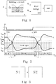
- a driving circuit 1 for driving half bridge connected electrically controlled power switches PT1, PT2in terms of having a near zero interlock delay (NZID) time between on-states of the power switches PT1, PT2.
- the interlock delay ID is known as the time interval, which is necessary between switching the load from a first power switch PT1 to a second power switch PT2 and back from the second power switch PT2 to the first power switch PT1 in order to prevent a cross-conduction through the power switches PT1 and PT2.
- a body diode D B conducts a load current I L .
- the body diode D B is either a parasitic diode of a power switch PT1,PT2 or a diode connected in parallel of the respective power switch PT1 or PT2.
- the body diode D B conducts in a source drain direction of the power switch PT1 or PT2.
- the load current I L causes charge carriers to develop within the body diode D B . These charge carriers cause unwanted current spikes when one power switch PT1 or PT2 starts to overtake the load current I L from the body diode D B of the other power switch PT2 or PT1.
- An interlock delay ID under 100 nsec influences the amount of the charge carriers developed in the body diode D B .
- the term near zero interlock (NZID) refers to an interlock delay, which is short enough for the charge carriers in the body diode D B not to occur.
- a load can be connected to the output of the half bridge HB.
- the half bridge HB is formed by the first power switch PT1 and the second power switch PT2.
- the power switch PT1 and PT2 can be one switching element PT1a, PT1b ... PT1n, PT2a, PT2b ... PT2n or a plurality of aforementioned switching elements connected in an arbitrary interconnection, whether parallel, serial or a combination of both.
- the switching element PT1a, PT1b ... PT1n, PT2a, PT2b ... PT2n can be any electrically controlled switching element on a semiconductor basis such as Si, SiC, GaN,...
- each power switch PT1 and PT2 consists of a FET cell FC and the aforementioned body diode D B .
- an additional diode is connected in parallel to each power switch PT1, PT2, such that the body diode D B conducts in the source to drain direction as shown in Fig. 12 .
- the driving circuit 1 shown in Fig. 1 receives an input signal A.
- the input signal A can for example be a pulse width modulated (PWM) signal or a pulse density modulated (PDM) signal.
- the driving circuit 1 generates at least one first drive signal J 1 and at least one second drive signal J 2 , that switches between on and off states in response to every rising and falling edge of the input signal A.
- the first drive signals J 1 controls the first power switch PT1
- the second drive signal J 2 controls the second power switch PT2.
- Each switching element PT1a, PT1b ... PT1n that forms the first power switch PT1 is driven with the drive signals J 1 and each switching element PT2a, PT2b ...
- the PT2n that forms the power switch PT2 is driven with the second drive signals J 2 .
- the on state value of the drive signals J 1 and J 2 holds the corresponding power switch PT1 or PT2 on.
- the off state value of the drive signals J 1 and J 2 holds the corresponding power switch PT1 or PT2 off.
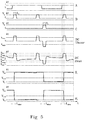
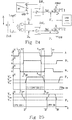
- the functionality of the driving circuit 1 is demonstrated by exemplary time curves of an example of a soft and hard switch of a half bridge HB made of Si MOSFET power switches PT1 and PT2 in Fig. 2 , wherein the switch waveforms on the left show a soft switching and the switch waveforms on the right show a hard switching.
- the soft switching occurs when the load current I L is transferred from the first power switch PT1 to the second power switch PT2 and hard switching occurs when the load current I L is transferred from the second power switch PT2 to the first power switch PT1.
- the first drive signal J 1 controls the corresponding first power switch PT1
- the second drive signal J 2 controls the corresponding second power switch PT2.
- the positive DC gate supply voltage V G+ represents the on state value of the drive signals J 1 and J 2 .
- the negative DC gate supply voltage V G- represents the off state value of the drive signals J 1 and J 2 .
- the corresponding power switch PT1, PT2 is deep in the cutoff region and is therefore switched off.
- the cutoff region represents the voltage range of a voltage applied to the control electrode of the power switch PT, which ensures that the respective power switch PT is not conducting.
- the on state value of the first drive signal J 1 holds the first power switch PT1 on and the off state value of the second drive signal J 2 holds the second power switch PT2 off.
- the on state value of drive signals J 1 and J 2 is the positive DC gate supply voltage V G+ and the off state value of drive signals J 1 and J 2 is the negative DC gate supply voltage V G- .
- the drive signals J 1 and J 2 After the stepwise change of the input signal A followed by a high-to-low propagation delay t HLpd the drive signals J 1 and J 2 start to switch their voltage values.
- the first drive signal J 1 starts decreasing its value from the on state voltage.
- the first power switch PT1 remains within the ohmic region until the drive signal J 1 reaches the load current threshold voltage V th@IL . At this point the first power switch PT1 comes into the active region and starts to switch off.
- the drain source voltage of the first power switch PT1 increases very fast to the DC link voltage being defined by the summation of power source voltages POWER+ and POWER-.
- This voltage change causes a current through the drain gate capacity C GD of the first power switch PTlwhich holds the first drive signal J 1 value constant until the time when the drain source voltage of the first power switch PT1 increases to the value of the DC link voltage.
- This effect is known as the so called Miller effect and appears simultaneously also on the second drive signal J 2 , as the drain source voltage change occurs also on the second power switch PT2.
- the second power switch PT2 is meanwhile still deeply in the cutoff region and there are no effects on the state of the second power switch PT2.After the voltage transition on the power switches PT1 and PT2 has been finished the first drive voltage J 1 continues to decrease.
- the current through the first power switch PT1 starts decreasing and drops to a value 0A at the time when the first drive voltage J 1 becomes equal to the threshold voltage V th .
- the first switch PT1 is off.
- the first drive voltage J 1 keeps decreasing without any further influence to the state of the first power switch PT1. Since the second drive voltage J 2 is still in the cutoff region and remains this way until it reaches the threshold voltage V th both power switches PT1 and PT2 are off simultaneously for the interlock delay ID time.
- the drive signals J 1 and J 2 are mirrored with respect to the mirroring voltage value V m at least for the transition time t t .
- the transition time t t represents the time interval in which the value of both drive signals J 1 and J 2 is lower than the threshold voltage V th of power switches PT1 and PT2, which is ensured by the mirroring voltage V m being lower than the threshold voltage V th of the power switches PT1 and PT2. Therefore the mirroring voltage Vmis within the so called cutoff region. Within the cutoff region the power switches PT1 and PT2 are turned off.
- the slope of the drive signals J 1 and J 2 and the mirror voltage V m define the value of the interlock delay ID.
- the value of the interlock delay ID can reach down to 4nsec while still remaining stable.
- the most important parameter for the interlock delay ID adjustment is the mirror voltage V m .
- the value of the mirroring voltage V m is adjustable as it is defined as the middle voltage between the DC gate supply voltages V G+ and V G- that can be controlled via the gate supply switching circuit 10 shown in Fig. 8 . This short interlock delay ID prevents any cross-conduction through the power switches PT1 and PT2.
- the second drive voltage J 2 increases its value from the threshold voltage V th to the load current threshold voltage V th@IL the load current I L from the body diode D B is transferred to the FET cell FC of the second power switch PT2.
- the second power switch PT2 is turned on. The further increase of the second drive voltage J 2 pushes the second power switch PT2 even deeper into the ohmic region.
- the shaping of the ramp of the drive signals J 1 and J 2 is performed by the ramp generating circuit 6 1 and 6 2 formed by inductances L 1 and L 2 as shown in Fig. 4 .
- the switching time t s a part of the driving energy is stored in inductances L 1 and L 2 .
- the switching time t s is defined as the time between the individual drive signal J 1 or J 2 changing its value from the on state voltage to the negative DC gate supply voltage V G- or vice versa from the off state voltage to the positive DC gate supply voltage V G+ .
- the stored energy extends the slope of the first drive signal J 1 under the negative DC gate supply voltage V G- and the slope of the second drive signal J 2 over the positive DC gate supply voltage V G+ by causing an oversway.
- the over sway magnitude V OS+ and V OS- is in the embodiment shown in Fig. 4 defined by a damping resistors R 1 and R 2 .
- the second drive voltage J 2 stays stable at the level of positive DC gate supply voltage V G+ and the first drive voltage J 1 stays stable at the level of the negative DC gate supply voltage V G- and consequently the second power switchPT2stays switched on whereas the first power switch PT1 stays switched off.
- the drive signals J 1 and J 2 respond to the rising edge of the input signal A with a low-to-high propagation delay t LHpd .
- the second drive signal J 2 starts decreasing its value from the on state voltage.
- the body diode of the second power switch PT2 overtakes the load current I L from the FET-cell of the power switch PT2.
- the situation of the conducting states of the power switches PT1 and PT2 stays unchanged for the interlock delay ID time until the rising first drive signal J 1 reaches the threshold voltage V th .
- the value of the interlock delay ID is the same as for the soft switching shown as the left side waveforms in Fig. 2 , since the mirroring voltage V m and the slope defined by inductances L 1 and L 2 of the drive signals J 1 and J 2 stay unchanged.
- the short value of the interlock delay ID prevents the charge carriers to occur. Therefore the body diode DB operates as an ideal diode without any reverse recovery effect for the time of the power switch PT1 overtaking the load current I L .
- the load current I L overtaking is finished when the first drive signal J 1 reaches the load current threshold voltage V th@IL .
- the Miller effect occurs.
- the values of the drive signals J 1 and J 2 remain unchanged until the drain source voltage at the second power switch PT2 is increased to the DC link voltage and the drain source voltage at the first power switch PT1 falls to I L *R ds_onPT1 .
- the on resistanceR ds_onPT1 of the first power switch PT1 is the drain source resistance of the switched on power switch PT1.
- the further increase of the first drive voltage J 1 pushes the first power switch PT1 even deeper into the ohmic region.
- the energy stored within the switching time t s prolongs the slope of the second drive signal J 2 under the DC gate supply voltage V G- and the slope of the first drive signal J 1 over the DC gate supply voltage V G+ by causing an over sway.
- the first drive voltage J 1 stays stable at the value of the positive DC gate supply voltage V G+ and the second drive voltage J 2 stays stable at the value of the negative DC gate supply voltage V G- and consequently the first power switch PT1 stays switched on and the second power switch PT2 stays switched off.
- the possible difference in propagation delays t HLpd and t LHpd according to the present invention has absolutely no influence on the interlock delay ID value. It only influences the value of the PWM ratio of the output PWM signal K with respect to the input PWM signal A.
- Fig. 3 shows a flow chart of a possible embodiment of the method for driving a half bridge HB in terms of having a near zero interlock delay NZID time between an on state of the power switches PT1 and PT2 according to the present invention.
- a first step S1 the triggering signals F 1 and F 2 are generated.
- a first triggering signal F 1 changes as a response to every odd step change of the input signal A its value in a stepwise from an on-voltage state to a positive DC gate supply voltage V G+ simultaneously with a second triggering signal F 2 which changes as a response to every even step change of the input signal its value in a stepwise from an off-voltage state to a negative DC gate supply voltage (V G- ).
- the drive signals J 1 and J 2 switch the corresponding power switches PT1 and PT2 between the on and off states.
- the drive signals J 1 and J 2 are mirrored with respect to one another along the mirroring voltage V m at least within the transition time t t .
- the mirroring voltage value V m is the voltage value applied to the control electrode of the power switches PT1 and PT2 that ensures both power switches PT1 and PT2 to be within the cutoff region.
- the transition time t t is defined as the time when none of the power switchesPT1, PT2 is in the so-called ohmic region.
- a power switch is in the ohmic region, when it is driven by a drive signal (J 1 or J 2 ) applied to the control electrode being larger as needed for ensuring the conduction of the load current I L .
- this region is called saturation.
- the driving circuit 1 of Fig. 4 comprises a differentiating circuit 4, a magnetic triggering circuit T1, triggering circuits 5 1 and 5 2 , ramp generating circuits 6 1 and 6 2 , a magnetic coupling circuit T3 and resistors R 1 and R 2 .
- the input signal A of the driving circuit 1 is connected to the differentiating circuit 4, which generates pulsed signals B and C.
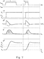
- the waveforms of the pulsed signals B and C are shown as a signal diagram in the second and third time curve of Fig. 5 .
- a pulse of the pulsed signal B is generated in response to the rising edge of the input signal A and a pulse of the pulsed signal C is generated in response to falling edge of the input signal A.
- the duration of these pulses is equal to an establishment time t e , which is either predetermined or defined simultaneously with the operation according to a power switch state information I T3 .
- the differentiating circuit 4 can generate maintenance pulses with the same polarity as the last pulse before.
- Maintenance pulses hold the drive signals J 1 and J 2 stable for an infinite time, especially in the case of a 0% or 100% duty cycle.
- a maintenance pulse is shown on the pulsed signal B in the second time curve of Fig. 5 .Each pulse of the pulsed signals B and C is amplified within the differentiating circuit 4 to a value, which has to be high enough for the pulsed signals B and C to control the triggering switches Q1 and Q2 through the magnetic triggering circuit T1 without any additional amplification.
- the magnetic triggering circuit T1 comprises a transformer with one primary and four secondary windings. Each side of the primary winding is connected to receive a pulsed signal B or C and each secondary winding is connected to one triggering transistor Q1 or Q2 of the triggering circuits 5 1 and 5 2 .
- the magnetic triggering circuit T1 converts the pulsed signals B and C to a bipolar trigger signal BC with the magnitude V Tr1 and V Tr2 being higher than the bipolar threshold voltage V thQ1 and V thQ2 of a corresponding triggering switch Q1 or Q2.
- the quality of the magnetic triggering circuit T1 ensures a demagnetization over sway V OS1 and V OS2 value being lower than the bipolar threshold voltage V thQ1 and V thQ2 .
- the theoretical waveform of the bipolar trigger signal BC is shown as the fourth time curve of Fig. 5 and the real waveform of the bipolar trigger signal BC is shown as the fifth time curve in Fig. 5 .
- the winding orientation of the magnetic triggering circuit T1 is provided in such a way to ensure that the active state of the pulsed signal B does turn on the first triggering transistor Q1 of the first triggering circuit 5 1 and the second triggering transistor Q2 of the second triggering circuit 5 2 simultaneously and to ensure that the active state of the pulsed signal C does turn on the second triggering transistor Q2 of the first triggering circuit 5 1 and the first triggering transistor Q1 of the second triggering circuit 5 2 simultaneously.
- the triggering switches Q1 and Q2 can be any electrically controlled switching element or a combination of such electrically controlled switching elements.
- the trigger switches Q1 and Q2 are serial connected and powered via the DC gate supply circuit.
- the first trigger switches Q1 connect the common point of the trigger switches Q1 and Q2 to the positive DC gate supply voltage V G+ .
- the second trigger switches Q2 connect the common point of the trigger switches Q1 and Q2 to the negative DC gate supply voltage V G- .
- the voltage at the common point of the triggering switches Q1 and Q2 of first triggering circuit 5 1 is the first triggering signal F 1 .
- the voltage at the common point of the triggering switches Q1 and Q2 of the second triggering circuit 5 2 forms the second triggering signal F 2 .
- the first triggering signal F 1 is shown as the sixth time curve in Fig.5 and the second triggering signal F 2 is shown as the seventh time curve in Fig.5 .
- the positive DC gate supply voltage V G+ represents the on-state voltage of the trigger signals F 1 and F 2 and the negative DC gate supply voltage V G- represents the off-state voltage of the trigger signals F 1 and F 2 .
- Both triggering signals F 1 and F 2 are grounded to a DC gate supply voltage V GND by means of a security resistance R off .
- the simultaneity of the switching of the first triggering switch Q1 of the first triggering circuit 5 1 and the second triggering switch Q2 of second triggering circuit 5 2 guaranteed by the magnetic triggering circuit T1 ensures a complementary switch-on of the first triggering signal F 1 and switch-off of the second triggering signal F 2 .
- the simultaneity of the switching of the second triggering switch Q2 of the first triggering circuit 5 1 and the first triggering switch Q1 of the second triggering circuit 5 2 guaranteed by the magnetic triggering circuit T1 ensures a complementary switch-on of the second triggering signal F 2 and switch-off of the first triggering signal F 1 .
- the triggering circuits 5 1 and 5 2 bothinclude a DC gate supply circuit 7.
- the DC gate supply circuit 7 supplies DC gate supply voltages V G+ , V G- and V GND to the triggering switches Q1 and Q2.
- a first energy E 1 powers the DC supply circuit 7 of the first triggering circuit 5 1 and a second energy E 2 powers the DC supply circuit 7 of the second triggering circuit 5 2 .
- the security resistance R off ensures that the voltage of the control electrode G is 0V, which in turn ensures that all power switches PT1 and PT2 of the normally off type are switched off and that the turn off of the power switches PT1, PT2 is executed in the absence of the bipolar pulsed signal BC.
- the security resistance R off causes a voltage drop of the triggering signals F 1 and F 2 in the time of an inactive bipolar pulsed signal BC.
- the maintenance pulse returns the dropped voltage value of the triggering signals F 1 and F 2 back to the previous value.
- Conversion of the first triggering signal F 1 into the first drive signal J 1 is performed by a corresponding first ramp generating circuit 6 1 , which is formed by an energy buffer component comprising an inductor L 1 .
- Conversion of the second triggering signal F 2 into the second drive signal J 2 is performed by a corresponding second ramp generating circuit 6 2 , which is formed by an energy buffer component comprising an inductor L 2 .
- the first drive signal J 1 is applied to the control electrode G of the first power switch PT1 and the second drive signal J 2 is applied to the control electrode G of the second power switch PT2.
- the above mentioned conversion of the triggering signals F 1 and F 2 into corresponding drive signal J 1 and J 2 causes a difference in the integral of the triggering signal F 1 or F 2 and the integral of the corresponding drive signal J 1 or J 2 .
- the first drive signal J 1 and the voltage difference area A VD are shown as the sixth time curve of Fig.
- the stepwise change of the triggering signal F 1 or F 2 causes a voltage difference on the corresponding inductor L 1 or L 2 with a maximum value of the voltage difference of the stepwise change of the triggering signal F 1 or F 2 , which drops to 0V within the switching time t s . Therefore a current I L1 , I L2 through the corresponding inductor L 1 , L 2 starts increasing and after that the switching time t s reaches a maximum value.
- the maximum values of currents I L1 and I L2 are defined by the voltage difference area A VD and the corresponding inductor L 1 or L 2 .
- the inductor current I L1 is shown as the fifth curve of Fig. 6 .
- the energy stored in the inductors L 1 and L 2 due to the corresponding current I L1 and I L2 generates an over sway on the corresponding drive signals J 1 or J 2 .
- a first resistor R 1 is connected in parallel to the first ramp generating circuit 6 1 and a second resistor R 2 is connected in parallel to the second ramp generating circuit 6 2 in order to prevent the rising of the corresponding drive signal J 1 and J 2 after the over sway.
- the resistor current I R1 is shown as the fourth curve of Fig. 6 .
- the mirroring of the voltage difference between the triggering voltage F 1 and the first drive voltage J 1 with respect to the voltage difference between the triggering voltage F 2 and the second drive voltage J 2 is performed by means of a magnetic coupling circuit T3.
- the magnetic coupling circuit T3 is formed by one transformer having its primary winding connected in parallel to the first ramp generating circuit 6 1 and having its secondary winding connected in parallel to the second ramp generating circuit 6 2 .
- the primary to secondary winding ratio is -1.
- the mirroring is performed by an equalizing current I eq flowing through the magnetic coupling circuit T3 windings during the time when one of the triggering switches Q1 or Q2 of both triggering circuits 5 1 and 5 2 conduct in any direction.
- Equal values of the inductance of the inductors L 1 and L 2 as well as equal values of the resistance of the resistors R 1 and R 2 reduce the equalizing current I eq through the magnetic coupling circuit T3.
- the establishment status information Inf e is transferred to the differentiating circuit 4.
- Theadditionally winding represents the voltage on the ramp generating circuits 6 1 and 6 2 , which forms simultaneously the establishment status information Inf e .
- the establishment status information is an indicator of the current switch state of the corresponding power switch PT1 or PT2.
- a significant information about the switching status is the time t Ie in which the establishment status information Inf e reaches a value 0 after having reached its maximum value.
- the over sway value after time t Ie represents the oversway in the drive signals J 1 and J 2 .
- Fig. 7 shows a comparison of a large establishment time t e on the left and a short establishment time t e on the right side.
- the first time curve in Fig.7 shows a bipolar pulsed signal BC with a marked up establishment time t e .
- the second time curve in Fig. 7 shows the first triggering signal F 1 .
- the third time curve in Fig. 7 shows an establishment time information Inf e with a marked up time t Ie .
- the fourth time curve in Fig. 7 shows the current I L1 with a marked up driving energy E L1 .
- the fifth time curve in Fig. 7 shows the first drive signal J 1 .
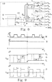
- the energy for driving the power switches PT1 and PT2 is supplied via the powering circuit 13 as shown in Fig. 8 .
- the powering circuit 13 comprises at least a supply switching circuit 10 and a power supply magnetic circuit T2.
- the gate switching circuit 10 generates a signal 0 by switching a gate power source voltage N by means of a switch SW1 in a ratio defined by a gate power ratio control signal M.
- the coupling capacitor C 5 prevents the power supply magnetic circuit T2 to saturate.
- the signal 0 carries an energy E T2 , which is transferred through the magnetic coupling circuit T2 to the DC gate supply circuits 7.
- the amplitude of the signal 0 is defined by the magnitude of the gate power source voltage N.
- the PWM ratio of the signal 0 is defined by the duty cycle of the gate power ratio control signal M.
- a bigger duty cycle of the gate power ratio control signal M simultaneously lowers the positive DC gate supply voltage V G+ and increases the negative DC gate supply voltage V G- and vice versa a lower duty cycle of the gate power ratio control signal M simultaneously increases the positive DC gate supply voltage V G+ and reduces the negative DC gate supply voltage V G- .
- This is ensured by the power supply magnetic circuit T2 due to its property of equalizing the positive voltage integral areas ⁇ 1 and ⁇ 2 and the negative voltage integral areas ⁇ 1' and ⁇ 2' of the signal 0.
- the amplitude and the PWM ratio of signal 0 defines the value of the DC gate supply voltages V G+ and V G- .
- the values of the DC gate supply voltages V G+ and V G- have both a linear dependency of the gate power source voltage N. Hence, by controlling the values of the gate power ratio signal M and the gate power source voltage N the DC gate supply voltages V G+ and V G- can be adapted.
- Fig. 9 shows the time diagrams of two examples of setting the DC gate supply voltages V G+ and V G- . Both examples are shown separately with a dotted line. On the left side of the dotted line an example of a bigger duty cycle of the gate power ratio signal M and a higher value of the gate power source voltage N is shown. On the right side of the dotted line an example of a smaller duty cycle of the gate power ratio signal M and a lower value of the gate power source voltage N is shown.
- the first time curve of the Fig. 9 shows the gate power ratio signal M
- the second time curve of the Fig. 9 shows gate power source voltage N
- the third time curve of the Fig. 9 shows the signal O with illustrated DC gate supply voltages V G+ and V G- as a response of the corresponding gate power ratio signal M and the corresponding gate power source voltage N.
- FIG. 8 A detailed schematic diagram of the DC gate supply circuit 7 is illustrated in Fig. 8 .
- Each DC gate supply voltage V G1+ , V G+ , V G- , V GND is generated by one half wave rectifier D 1 or D 2 or D 3 and a corresponding smoothing capacitor C 1 or C 2 or C 3 .
- the DC gate supply voltages V G+ and V G- are powered though the same winding.
- an additional tap T' on the corresponding secondary winding of the power supply magnetic circuit T2 is used.
- the signal 0 voltage output by the secondary winding of the power supply magnetic circuit T2 is used to define a shut down information Inf SD .
- a shut down information Inf SD Inf SD .
- An operating period time t op reduces to a shut down period time t sd , which is detected by the shut down circuit 8.
- the connection of the shut down circuit 8 is shown in Figs. 15-16 .
- the DC gate source voltages V G+ and V G- and consequently also the average voltage value of the DC gate source voltages V G+ and V G- , namely the mirroring voltage V m is defined.
- Setting of the DC gate source voltages V G+ and V G- and the mirroring voltage V m is limited by the condition that the mirroring voltage V m needs to be below the threshold voltage V th value.
- the time curves of the drive signals J 1 and J 2 in Fig. 10 of one possible embodiment show the difference in the interlock delay ID for two different values of the DC gate supply voltages V G+ and V G- .
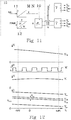
- Fig. 11 shows a possible embodiment of a circuit which ensures a stable interlock delay ID regardless the temperature changes of the power switches PT1 and PT2.With the temperature increase a drop in the threshold voltage V th occurs as shown in the first time curve of Fig. 12 . Therefore the mirroring voltage V m needs to change with the same voltage difference over the entire temperature range of the power switches PT1 and PT2.
- a temperature influence adapting circuit 11 and a DC/DC converter is added to the powering circuit 13.
- the temperature influence adapting circuit 11 adjusts the gate power ratio control signal M and controls a DC/DC converter 12 so that the DC/DC converter 12 generates a gate power source voltage N with respect to a temperature information Inf T .
- the voltage difference V dif is the voltage difference between the mirroring voltage V m and the threshold voltage V th .
- the temperature information Inf T includes an information about the junction temperature T J of the power switches PT1 and PT2.
- the first time curve in Fig. 12 illustrates a possible example of the threshold voltage V th dependence on the junction temperature T J .
- the second and third time curves in Fig. 12 show the gate power ratio control signal M and the gate power source voltage N as a response to the temperature information Inf T with respect to the junction temperature T J .
- the fourth time curve in Fig. 12 shows the voltage difference V dif , which is constant throughout the entire junction temperature T J range of the power switches PT1 and PT2 and the corresponding DC gate supply voltages V G+ and V G- that ensure such a constant voltage difference V dif .
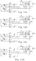
- Figs. 13a-13d an energy return for on switching of the first power switch PT1 is demonstrated and in Figs. 14a-14d an energy return for off switching of the first power switch PT1 is demonstrated. Only the elements that are included in the energy transfer of the first power switch PT1 are shown.
- the circuit in Figs. 14a-14d has an additional tap T and additional capping diodes D 6 and D 7 added with respect to the part of the driving circuit 1 that controls the first power switch PT1 in the embodiment shown in Fig. 4 .
- the magnetic coupling circuit T3 has an additional tap T on the winding connected to inductor L 1 of the first ramp generating circuit 6 1 to form an autotransformer function.
- the position of the tap T is set closer to the side of the winding, which is connected to the control electrode G of the first power switch PT1 and forms a coupling ratio R C ⁇ 1 between 0.5 and 1.
- the capping diode D 6 is connected to the tap T to receive the DC gate supply voltage V G+ of the DC gate supply circuit 7.
- the capping diode D 7 is connected between the negative DC gate supply voltage V G- of the DC gate supply circuit 7 and the tap T.
- the triggering switch Q1 is switched on and a gate current I G1 transfers the driving energy from the smoothing capacitor C 1 to capacitor C GS .
- the gate current I G1 flows via the inductor L 1 the value of the energy stored in the inductor L 1 is equal to the value of the energy stored in the capacitor C GS .
- the gate current I G1 still flows due to the energy stored in the inductor L 1 within the establishment time t e .
- the energy is transferred from inductor L 1 to the capacitor C GS and the smoothing capacitor C 2 .
- the part of the energy that is returned to the smoothing capacitor C 2 is the energy, which is returned back to the DC power supply circuit 7.
- the drive signal J 1 voltage value reaching the DC gate supply voltage V G+ divided by the coupling ratio R C ⁇ 1 the gate current I G1 drops to 0 and the energy, which is still stored in the inductor L 1 is transferred through the capping diode D 6 to the smoothing capacitors C 1 and C 2 of the DC power supply circuit 7 as shown in Fig. 13c .
- the energy stored in capacitor C GS due to the oversway is returned back to the smoothing capacitor C 1 of the DC gate supply circuit 7 through the capping diode D 6 as shown in Fig. 13d .
- the triggering switch Q2 is switched on and a gate current I G1 transfers the driving energy from smoothing capacitor C 2 to capacitor C GS .
- the gate current I G1 flows via the inductor L 1 the value of the energy stored in the inductor L 1 is equal to the value of the energy stored in the capacitor C GS .
- the gate current I G1 still flows due to the energy stored in the inductor L 1 within the establishment time t e .
- the energy is transferred from inductor L 1 to capacitor C GS and the smoothing capacitor C 1 .
- the part of the energy that is returned to the smoothing capacitor C 1 is the energy, which is returned back to the DC power supply circuit 7.
- the drive signal J 1 voltage value reaching the DC gate supply voltage V G+ divided by the coupling ratio R C ⁇ 1 the gate current I G1 drops to 0 and the energy, which is still stored in the inductor L 1 is transferred through the capping diode D 7 to the smoothing capacitors C 1 and C 2 of the DC power supply circuit 7 as shown in Fig. 14c .
- the energy stored in capacitor C GS due to the oversway is returned back to the smoothing capacitor C 2 of the DC gate supply circuit 7 through the capping diode D 7 as shown in Fig. 14d .
- the power switches PT1 and PT2 are formed by switching elements such as BJTs or JFETs, which demand a constant current into the control electrode G to hold the power switch PT1 and PT2 on or off.
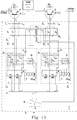
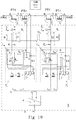
- Fig. 15 shows a possible embodiment of the driving circuit 1 driving the half bridge HB connected BJTs as power switches PT1 and PT2.
- Fig. 16 shows a possible embodiment of the driving circuit 1 driving the in half bridge HB connected JFETs as power switches PT1 and PT2.
- a bistable circuit 9 is connected to the triggering circuits 5 1 and 5 2 in order to provide a constant current flowing to the control electrode G of the power switches PT1 and PT2.
- the bistable circuit 9 is powered via the DC gate supply circuit 7 with the DC gate supply voltages V G1+ and V G- and consists of two current generators Ion and I off , a comparator X and a bistable circuit resistor R bc .
- the comparator X has a hysteresis of approximately 1V with respect to DC gate supply voltage V GND . At the time the drive signals J 1 and J 2 being within the hysteresis area the comparator X does not switch the current generators I on or I off on.
- the comparator X switches the current generator I on on and at the time when the drive voltage is below the hysteresis the comparator X switches the current generator I off on.
- a bistable circuit resistor R bc is added in the feedback loop of the comparator X to prevent the current reduction at the time when the shut down circuit is turned on.
- the current generator I on is powered via the DC gate supply circuit 7 with the DC gate supply voltage V G1+ and generates a preset current value needed to hold the on-state of the corresponding power switch PT1 and PT2.
- the position of the tap T' on the secondary winding of the power supply magnetic circuit T2 defines the minimum value of the DC gate supply voltage V G1+ that still holds the voltage drop on the current generator Ion high enough for the current generator I on to be able to generate the preset current in all working condition.
- a recommended voltage drop on the current generator I on is up to 2 V.
- the current generator I off is powered via the DC gate supply circuit 7 with the negative DC gate supply voltage V G- and generates a current needed to hold the off-state of the corresponding power switch PT1 and PT2.
- the current generated by the current generator I off is predefined and has a value within the mA region and can therefore be replaced with a resistor.
- the shut down circuit 8 includes a decoding circuit, which detects a change in the frequency of the signal 0 and as a response to a detected shut down period time t sd deactivates the bistable circuit 9, connects the corresponding drive signal J 1 or J 2 to the DC gate supply voltage V GND and consequently turns the corresponding power switch PT1 or PT2 off.
- the driving circuit 1 controls BJTs as power switches PT1 and PT2, therefore the on state voltage V PT1on and V PT2on is lower than the DC gate supply voltage V G+ due to the properties of the BJTs.
- the triggering switch Q2 switches on a voltage difference between the DC gate supply voltage V G- and on state voltage V on occurs on the corresponding ramp generating circuit 6 1 or 6 2 .
- the triggering switch Q1 switches on a voltage difference between the DC gate supply voltage V G+ and the off state voltage V on occurs at the corresponding ramp generating circuits 6 1 or 6 2 .
- the short circuit current through the magnetic coupling circuit T3 due to the voltage difference that thus occurs between ramp generating circuit 6 1 or 6 2 is prevented by a blocking diode D 9 added to the triggering circuits 5 1 and 5 2 between the triggering switch Q2 and the negative DC gate supply voltage V G- of the DC gate supply circuit 7. Only an energy return through the capping diode D 7 is possible. Therefore only the capping diode D 7 is used for the energy return to the DC power supply circuit 7.
- the part of energy stored in the inductors L 1 and L 2 during the establishment time t e is only returned to the DC gate supply circuit 7, which belongs to the second power switch PT1 or PT2 that is turning off. Therefore the driving energy E L1 is during the switch off of the power switch PT2 transferred through the magnetic coupling circuit T3 and the driving energy E L2 is during the switch off of the first power switch PT1 transferred through the magnetic coupling circuit T3.
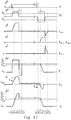
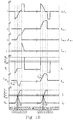
- the Figs. 17 and 18 show a response of the characteristic time curves with respect to the input signal A shown in the first time curve of the Fig. 17 .
- the time markers a-1 are equal for Fig. 17 and Fig. 18 .
- the time markers a and g present the beginning of the switching.
- the time markers b and h present the time when the bistable circuit 9 turns off the current generator I on .
- the time markers c and i represent the time when the bistable circuit 9 turns on the current generator I on .
- the time markers d and j represent the time when the triggering switch Q2 stops conducting due to the drive signals J 1 and J 2 being equal to the negative DC gate supply voltage V G- .
- the time markers e and k represent the time after the establishment time t e has expired.
- the time markers f and l represent the time when the energy return process is finished.
- the second time curve of the Fig. 17 shows a signal diagram of the bipolar pulsed signal BC with a marked up establishment time t e .
- the third time curve of the Fig. 17 shows a signal diagram of the current I Q1_1 of the triggering switch Q1 of the first triggering circuit 5 1 .
- the fourth time curve of the Fig. 17 shows a signal diagram of the current I Q2_1 of the triggering switch Q2 of the second triggering circuit 5 1 , which is equal to the current I D9_1 of the blocking diode D 9 of the same triggering circuit 5 1 .
- the fifth time curve of the Fig. 17 shows a signal diagram of the current I D7_1 of the capping diode D 7 of the first triggering circuit 5 1 .
- the sixth time curve of the Fig. 17 shows signal diagram of the first triggering signal F 1 .
- the seventh time curve of the Fig. 17 shows signal diagram of the current I G1 flowing to the control electrode of the first power switch PT1 with a marked up current I ON1 of the current generator I on .
- the eighth time curve of the Fig. 17 shows the signal diagram of the first drive signal J 1 .
- the first time curve of the Fig. 18 shows the signal diagram of the establishment time information Inf e .
- the second time curve of the Fig. 18 shows the signal diagram of the current I Q1_2 of the triggering switch Q1 of the second triggering circuit 5 2 .
- the third time curve of the Fig. 18 shows the signal diagram of the current I Q2_2 of the triggering switch Q2 of the second triggering circuit 5 2 , which is equal to the current I D9_2 of the blocking diode D 9 of the same triggering circuit 5 2 .
- the fourth time curve of the Fig. 18 shows signal diagram of the current I D7_2 of the capping diode D 7 of the second triggering circuit 5 2 .
- FIG. 17 shows signal diagram of the second triggering signal F 2 .
- the sixth time curve of the Fig. 18 shows signal diagram of the current I G2 flowing to the control electrode of the second power switch PT2 with a marked up current I ON1 of the current generator I on .
- the eighth time curve of the Fig. 17 shows the signal diagram of the drive signals J 1 and J 2 with a marked up interlock delay ID.
- the dot hatched area on the Fig. 18 shows the on and off states of the power switches PT1 and PT2.
- the driving circuit 1 controls normally on JFETs as power switches PT1 and PT2.
- the cascode power switch PTc is connected in a cascode with the first power switch PT1 and a cascode power switch PTc connected with the second power switch PT2 is added.
- a cascode power switch PTc is formed by a low voltage and low on resistance MOSFET.
- the voltage of the cascode power switch PTc needs to be high enough to hold the power switch PT1 or PT2 in the cutoff region when the voltage on the control electrode G of the power switch PT1 or PT2 reaches a positive DC gate supply voltage V G+ .
- the on resistance of the cascode power switch PTc should be in a mQ range in order for the cascode power switch PTc not to essentially contribute to the conductive losses of the half bridge HB.
- an off current generating resistor R IG -substitutes the off current generator I off and a cascode switching circuit 14 is added to the triggering circuits 5 1 and 5 2 in order to control the cascode power switch PTc.
- the cascode switching circuit 14 ensures an off state of the cascode power switch PTc during the establishment of the operation conditions of the driving circuit 1 by holding the control electrode G of the cascode power switch PTc connected to the source S of the cascode power switch PTc.
- the control electrode G of the power switch PT1 and PT2 is connected through the off current generating resistor R IG- to the DC gate supply voltage V G- and through the half wave rectifier D 2 and the corresponding secondary winding of the power supply magnetic circuit T2 back to the source S of the cascode power switch PTc.
- the cascode switching circuit 14 turns the cascode power switch PTcon.
- the corresponding power switch PT1 or PT2 remains in the cutoff region despite the cascode power switch PTc being turned on as the voltage at the control electrode G of the corresponding power switch PT1 or PT2 remains lower than the threshold voltage V th , namely at the level of the negative DC gate supply voltage V G- .
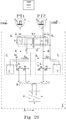
- SiC FETs are provided as power switches PT1 and PT2.
- SiC FETs are limited with a negative voltage to a maximum negative driving voltage -10V, have the threshold voltage V th in the range up to 3V and need up to +20V to be completely in the ohmic region.
- a blocking diode D 8 and the only the capping diode D 6 is added to the triggering circuit 5 1 and 5 2 .
- the DC gate supply voltage V G- is defined to be close to the maximum negative driving voltage, for example -8V for a -10V device limit.
- the mirroring voltage V m is defined to be within the cutoff region of the power switches PT1 and PT2.
- the positive DC gate supply voltage V G+ is equal V m + (V m - V G- ), where V m presents the mirroring voltage and V G- presents the DC gate supply voltage V G- .
- On state voltage V on is defined to be close to the maximum positive driving voltage, for example 20V for a -22V device limit with the autotransformer coupling ratio R C ⁇ 1 through the equation (V G+ - V G- ) / (V on - V G- ), where V on presents the on state voltage, V G+ represents the positive DC gate supply voltage and V G- represents the negative DC gate supply voltage.
- the driving energy E L1 and E L2 is in the possible embodiment of the Fig. 20 returned to the DC power supply circuit 7 of the triggering circuit 5 1 or 5 2 at the time of the corresponding power switch PT1, PT2 is switching on.
- the driving energy E L1 and E L2 is transferred through the magnetic coupling circuit T3 via the capping diode D 6 of the first triggering circuit 5 1 connected to the corresponding tap T of the magnetic coupling circuit T3 and returned back to the DC gate supply circuit 7of the first triggering circuit 5 1 at the time when the power switch PT1 is in the switch on transition.
- the driving energy E 1 and E L2 is transferred through the magnetic coupling circuit T3 via the capping diode D 6 of the second triggering circuit 5 2 connected to the corresponding tap T of the magnetic coupling circuit T3 and returned back to the DC gate supply circuit 7 of the second triggering circuit 5 2 at the time when the power switch PT2 is in the switch on transition.
- Fig. 21 illustrates simplified time curves of a switch off transition of the first power switch PT1 and a switch on transition of the second power switch PT2.
- the triggering switch Q1 of the first triggering circuit 5 1 and the triggering switch Q2 of the second triggering circuit 5 2 is switched on.
- the first drive signal J 1 starts to drop.
- the second drive signal J 2 remains stable on the value of the off state voltage V off due to the blocking diode D 8 .
- + V G+ the voltage on inductor L1 drops to a value
- the first drive signal J 1 starts to increase.
- the first drive voltage J 1 reaches the load current threshold voltage V th@IL and the output voltage K starts to drop.
- the Miller effect becomes effective.
- the dropping in the output voltage K after time markingt 3 speeds up due to the reduction of the gate-drain capacity of the first power switch PT1 when the gate drain voltage of the first power switch PT1 overtakes the gate source voltage of the power switch PT1.
- the difference between the gate drain capacities of the power switches PT1 and PT2 causes an equalizing current I eq flowing through the magnetic coupling circuit T3 between the time markings t 2 and t 3 .
- the load current I LPT1 transfers from the FET cell FC of the first power switch PT1 to the body diode D B of the second power switch PT2 during the time when the first drive signal J 1 drops to the threshold voltage V th which is reached at the time marking t 5 .
- the first power switch PT1 is off.
- the second drive signal J 2 increases to the threshold voltage V th .
- the load current I LPT2 is transferred from the body diode D B to the FET cell FC of the second power switch PT2 between the time markings t 6 and t 7 .
- the energy stored in the inductors L 1 and L 2 cause the second drive voltage J 2 to increase to on state voltage V on reached at the time marking t 8 .
- the energy stored in the inductor L 2 is transferred to the gate source capacity of the second power switch PT2 through the magnetic coupling circuit T3.Thisenergy transfer is shown by the equalizing current I eq flowing between the time markings t 7 and t 8 .
- the first time curve of Fig. 21 shows the signal diagram of the drive signals J 1 and J 2 .
- the second time curve of the Fig. 21 shows the signal diagram of the equalizing current I eq .
- the third time curve of Fig. 21 shows the signal diagram of the output signal K.
- the fourth time curve of Fig. 21 shows the signal diagram of the load current I LPT1 flowing through the first power switch PT1.
- the fifth time curve of the Fig. 21 shows the signal diagram of the current flowing through the body diode D B2 of the second power switch PT2.
- the sixth time curve of the Fig. 21 shows the signal diagram of the load current I LPT2 of the second power switch PT2.
- the first power switch PT1 consists of serially connected switching elements PT1a, PT1b ... PT1n and the second power switches PT2 consists of serially connected switching elements PT2a, PT2b ... PT2n.
- the first triggering circuit 5 1 comprises triggering circuits 5 1 a, 5 1 b ... 5 1 n and the second triggering circuit 5 2 comprises triggering circuits 5 2 a, 5 2 b ... 5 2 n.
- the triggering circuits 5 1 a, 5 1 b ... 5 1 n, 5 2 a, 5 2 b ... 5 2 n are driven with the magnetic triggering circuit T1.
- the magnetic triggering circuit T1 comprises six transformers each having one primary and two secondary winding.
- the first ramp generating circuit 6 1 consists of 6 1 a, 6 1 b ... 6 1 n and the second ramp generating circuit 6 2 consists of 6 2 a, 6 2 b ... 6 2 n.
- Each triggering circuit 5 1 a, 5 1 b ... 5 1 n, 5 2 a, 5 2 b ... 5 2 n is connected to a corresponding ramp generating circuit 6 1 a, 6 1 b ... 6 1 n, 6 2 a, 6 2 b ... 6 2 n being connected to the corresponding switching element PT1a, PT1b ... PT1n, PT2a, PT2b ...
- the resistor R 1 is connected in parallel to every ramp generating circuit 6 1 a, 6 1 b ... 6 1 n, 6 2 a, 6 2 b ... 6 2 n.
- the magnetic coupling circuit T3 consists of six transformers each having one of its windings connected to one of the ramp generating circuits 6 1 a, 6 1 b ... 6 1 n, 6 2 a, 6 2 b ... 6 2 n and the remaining windings connected in parallel between each other.
- 6 1 n is 1 and a coupling ratio between windings of the magnetic coupling circuit T3 connected to any pair of the ramp generating circuits 6 2 a, 6 2 b ... 6 2 n is 1.
- the coupling ratio between the windings of the magnetic coupling circuit T3 being connected to the ramp generating circuits 6 1 n and 6 2 n is -1.
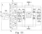
- the driving circuit 1 controls the first power switch PT1, which consists of two switching elements PTla and PT1b and the second power switch PT2, which consists of two switching elements PT2a and PT2b.
- the switching elements PTla and PT2a are also connected in a half bridge and the switching elements PT1b and PT2b are connected in a half bridge.
- the switching elements PTla and PT2b are powered with the power supply POWER+ and switching elements PT2a and PT1b are powered with the power supply POWER+.
- the load is connected between a common point of the switching elements PTla and PT2b and a common point of the switching elements PT2a and PT1b.
- the magnetic triggering circuit T1 has one transformer with one primary and eight secondary windings.
- the first triggering circuit 5 1 consists of two triggering circuits 5 1 a and 5 2 b and the second triggering circuit 5 2 consists of two triggering circuits 5 2 a and 5 1 b.
- the first ramp generating circuit 6 1 consists of two ramp generating circuits 6 1 a and 6 2 b and the second ramp generating circuit 6 2 consists of two ramp generating circuits 6 2 a and 6 1 b.
- the triggering circuit 5 1 a controls the switching element PTla through the ramp generating circuit 6 1 a
- the triggering circuit 5 2 a controls the switching element PT2a through the ramp generating circuit 6 2 a
- the triggering circuit 5 1 b controls the switching element PT1b through the ramp generating circuit 6 1 b
- the triggering circuit 5 2 b controls the switching element PT2b through the ramp generating circuit 6 2 b.
- a resistor R 1 is connected in parallel to the ramp generating circuits 6 1 a and 6 2 b.
- a resistor R 2 is connected in parallel to the ramp generating circuits 6 2 a and 6 1 b.
- the magnetic coupling circuit T3 is formed by two transformers each having windings connected in parallel to the ramp generating circuits 6 1 a, 6 2 a, 6 1 b and 6 2 b as shown in Fig. 23 .
Landscapes
- Engineering & Computer Science (AREA)
- Physics & Mathematics (AREA)
- Computer Hardware Design (AREA)
- Computing Systems (AREA)
- General Engineering & Computer Science (AREA)
- Mathematical Physics (AREA)
- Power Engineering (AREA)
- Electronic Switches (AREA)
- Power Conversion In General (AREA)
- Dc-Dc Converters (AREA)
- Inverter Devices (AREA)
Claims (15)
- Circuit d'attaque (1) destiné à attaquer des interrupteurs de puissance à commande électrique montés en demi-pont (PT1, PT2) avec un temps de retard de verrouillage quasi nul (NZID, near zero interlock delay time) entre des états passants des interrupteurs de puissance (PT1, PT2), dans lequel le circuit d'attaque (1) est conçu pour recevoir un signal d'entrée (A) et pour produire :- un premier signal d'attaque (J1) qui est destiné à commuter un premier interrupteur de puissance (PT1) entre l'état passant et bloqué,- un second signal d'attaque (J2) qui est destiné à commuter un second interrupteur de puissance (PT2) entre l'état passant et bloqué,dans lequel à chaque variation impaire en échelon du signal d'entrée (A), le premier signal d'attaque (J1) se met à augmenter sa valeur par le biais d'une pente, d'une tension négative d'alimentation de grille en courant continu (VG-) à une tension positive d'alimentation de grille en courant continu (VG+) et le second signal d'attaque (J2) se met à diminuer sa valeur, d'une tension positive d'alimentation de grille en courant continu (VG+) à une tension négative d'alimentation de grille en courant continu (VG-) ,
dans lequel à chaque variation paire en échelon du signal d'entrée (A), le premier signal d'attaque (J1) se met à diminuer sa valeur par le biais d'une pente, d'une tension positive d'alimentation de grille en courant continu (VG+) à une tension négative d'alimentation de grille en courant continu (VG-) et le second signal d'attaque (J2) se met à augmenter sa valeur, d'une tension négative d'alimentation de grille en courant continu (VG-) à une tension positive d'alimentation de grille en courant continu (VG+),
dans lequel la valeur de ladite pente définit la valeur d'un retard de verrouillage (ID)
dans lequel le retard de verrouillage (ID) est le temps entre des états passants du premier interrupteur (PT1) et du second interrupteur (PT2),
dans lequel l'expression « retard de verrouillage quasi nul » (NZID) désigne un retard de verrouillage qui est assez court pour que des porteurs de charge dans la diode de structure (DB) n'apparaissent pas,
dans lequel la tension négative d'alimentation de grille en courant continu (VG-) pousse le premier interrupteur de puissance (PT1) et le second interrupteur de puissance (PT2) profondément dans une région de coupure, dans lequel la tension positive d'alimentation de grille en courant continu (VG+) pousse le premier interrupteur de puissance (PT1) et le second interrupteur de puissance (PT2) profondément dans une région ohmique,
dans laquelle la courbe de signal du premier signal d'attaque (J1) est en miroir par rapport à la courbe de signal du second signal d'attaque (J2) le long d'un axe temporel d'une valeur de tension de réflexion (Vm) à l'intérieur d'un temps de transition (tt), dans lequel la valeur de tension de réflexion (Vm) se définit comme une tension médiane entre la tension positive d'alimentation de grille en courant continu (VG+) et la tension négative d'alimentation de grille en courant continu (VG-) et
dans lequel la tension positive d'alimentation de grille en courant continu (VG+) et la tension négative d'alimentation de grille en courant continu (VG-) sont ajustées de manière que la valeur de tension de réflexion (Vm) se situe dans la région de coupure des interrupteurs de puissance (PT1, PT2). - Circuit d'attaque selon la revendication 1, comprenant :- au moins un premier circuit générateur de signal de déclenchement (51, 51a, 51b ... 51n),- au moins un second circuit générateur de signal de déclenchement (52, 52a, 52b ... 52n),- au moins un premier circuit générateur de rampe (61, 61a, 61b ... 61n) et- au moins un second circuit générateur de rampe 62, 62a, 62b ... 62n),dans lequel chaque circuit générateur de signal de déclenchement (51, 52, 51a, 51b, ... 51n ; 52a, 52b ... 52n) comprend une paire d'interrupteurs de déclenchement (Q1, Q2),
dans lequel chaque paire d'interrupteurs de déclenchement (Q1, Q2) du premier circuit générateur de signal de déclenchement (51, 51a, 51b ... 51n) est destiné à produire un premier signal de déclenchement (F1),
dans lequel chaque paire d'interrupteurs de déclenchement (Q1, Q2) du second circuit générateur de signal de déclenchement (52, 52a, 52b ... 52n) est destiné à produire un second signal de déclenchement (F2),
dans lequel, en conséquence de chaque variation logique impaire du signal d'entrée (A), un premier interrupteur de déclenchement (Q1) dudit premier circuit générateur de signal de déclenchement (51, 51a, 51b ... 51c) fait varier en échelon la valeur du premier signal de déclenchement (F1), d'un état hors tension (VPT1off) à une tension positive d'alimentation de grille en courant continu (VG+), en même temps qu'un second interrupteur de déclenchement (Q2) du second circuit générateur de signal de déclenchement (52, 52a, 52b ... 52n) fait varier en échelon la valeur du second signal de déclenchement (F2), d'un état sous tension (VPT2on) à une tension négative d'alimentation de grille en courant continu (VG-),
dans lequel, en conséquence de chaque variation logique paire du signal d'entrée (A), un premier interrupteur de déclenchement (Q1) du second circuit générateur de signal de déclenchement (52, 52a, 52b ... 52n) fait varier en échelon la valeur du second signal de déclenchement (F2), d'un état hors tension (VPT2off) à une alimentation de grille en courant continu positif (VG+), en même temps qu'un second interrupteur de déclenchement (Q2) du premier circuit générateur de signal de déclenchement (51, 51a, 51b ... 51c) fait varier en échelon la valeur du premier signal de déclenchement (F1), d'un état sous tension (VPT1on) à une tension négative d'alimentation de grille en courant continu (VG-) et
dans lequel chaque variation en échelon de tension du premier signal de déclenchement (F1) est mise en forme en premier signal d'attaque (J1) par formation d'une pente par le biais du premier circuit générateur de rampe (61, 61a, 61b ... 61n) et dans lequel chaque variation en échelon de tension du second signal de déclenchement (F2) est mise en forme en second signal d'attaque (J2) par formation d'une pente par le biais du second circuit générateur de rampe (62, 62a, 62b ... 62n). - Circuit d'attaque selon la revendication 1 ou 2,
dans lequel le premier circuit générateur de rampe (61, 61a, 61b ... 61n) comprend un composant formant tampon d'énergie, formé par une première inductance (L1) connectée entre un point commun de la paire d'interrupteurs de déclenchement (Q1, Q2) du premier circuit générateur de signal de déclenchement (51, 51a, 51b ... 51n) et une électrode de commande (G) du premier interrupteur de puissance (PT1) et dans lequel le second circuit générateur de rampe (62, 62a, 62b ... 62n) comprend un composant formant tampon d'énergie, formé par une seconde inductance (L2) connectée entre un point commun de la paire d'interrupteurs de déclenchement (Q1, Q2) du second circuit générateur de signal de déclenchement (52, 52a, 52b ... 52n) et une électrode de commande (G) du second interrupteur de puissance (PT2),
dans lequel la première inductance (L1) est destinée à fournir un courant maximum à l'électrode de commande (G) du premier interrupteur de puissance (PT1), au moment où une tension de seuil (Vth) dudit premier interrupteur de puissance (PT1) est atteinte,
dans lequel une première énergie d'attaque (EL1) stockée dans la première inductance (L1) à l'intérieur d'un temps de commutation (tS) est suffisamment élevée pour former un dépassement de tension sur l'électrode de commande (G) du premier interrupteur de puissance (PT1), afin d'accélérer la commutation du premier interrupteur de puissance (PT1), dans lequel la seconde inductance (L2) est destinée à fournir un courant maximum à l'électrode de commande (G) du second interrupteur de puissance (PT2), au moment où la tension de seuil (Vth) du second interrupteur de puissance (PT2) est atteinte et dans lequel la seconde énergie d'attaque (EL2) stockée dans la seconde inductance (L2) à l'intérieur d'un temps de commutation (tS) est suffisamment élevée pour former un dépassement de tension sur l'électrode de commande (G) du second interrupteur de puissance (PT2), ce qui accélère la commutation du second interrupteur de puissance (PT2). - Circuit d'attaque selon l'une des revendications 1 à 3 précédentes,
dans lequel une première résistance d'amortissement (R1) est connectée en parallèle à la première inductance (L1) et est destinée à amortir une oscillation de signal du premier signal d'attaque (J1) et
dans lequel une seconde résistance d'amortissement (R2) est connectée en parallèle à la seconde inductance (L2) et est destinée à amortir une oscillation de signal du second signal d'attaque (J2). - Circuit d'attaque selon l'une des revendications 1 à 4 précédentes,
dans lequel le circuit d'attaque (1) comprend un circuit de commutation d'alimentation de grille (10) et un circuit magnétique d'alimentation électrique (T2),
dans lequel chaque circuit générateur de signal de déclenchement (51, 51a, 51b ... 51n ; 52, 52a, 52b ... 52n) comprend un circuit d'alimentation de grille en courant continu (7),
dans lequel ledit circuit d'alimentation de grille en courant continu (7) comprend au moins un redresseur à simple alternance (D1, D2, D3) et au moins un condensateur de lissage (C1, C2, C3),
dans lequel chaque circuit d'alimentation de grille en courant continu (7) est destiné à :- produire au moins une tension positive d'alimentation de grille en courant continu (VG+, VG1+) et une tension négative d'alimentation de grille en courant continu (VG-) et pour- fournir au premier interrupteur de déclenchement (Q1) la tension positive d'alimentation de grille en courant continu (VG+)- fournir au second interrupteur de déclenchement (Q2) la tension négative d'alimentation de grille en courant continu (VG-) , et- recevoir de l'énergie en provenance dudit circuit magnétique d'alimentation électrique (T2)dans lequel chaque tension d'alimentation de grille en courant continu (VG+, VG1+, VG-) peut avoir la valeur de 0 V,
dans lequel ledit circuit de commutation d'alimentation de grille (10) est conçu pour :- recevoir un signal de réglage de rapport de puissance de grille (M),- recevoir une tension de source d'alimentation de grille en courant continu (N), et- produire un signal (O) destiné à être porteur d'une énergie d'alimentation de grille (ET2) ;dans lequel ledit circuit de commutation (10) ajuste la valeur de tension des tensions d'alimentation de grille en courant continu (VG+, VG1+, VG-) délivrées par le circuit d'alimentation de grille (7) en modulant la tension de source d'alimentation de grille en courant continu (N) reçue avec des informations de modulation de largeur d'impulsions du signal de réglage de rapport de puissance de grille (M) reçu,
dans lequel ledit circuit magnétique d'alimentation électrique (T2) comprend au moins un transformateur et est destiné à assurer un transfert d'énergie galvanique isolée de ladite énergie d'alimentation de grille (ET2), depuis le circuit de commutation d'alimentation (10) vers les deux circuits d'alimentation de grille en courant continu (7). - Circuit d'attaque selon la revendication 5,
dans lequel ledit circuit d'attaque (1) comprend un circuit d'adaptation à l'influence de la température (11) destiné à :- recevoir un signal d'information de température (InfT) porteur d'une information de température,- produire ledit signal de réglage de rapport de puissance de grille (M),- régler la valeur de ladite tension de source d'alimentation de grille en courant continu (N) par l'intermédiaire d'un convertisseur courant continu/courant continu (12) et- régler le un signal de réglage de rapport de puissance de grille (M) et la tension de source d'alimentation de grille en courant continu (N) par rapport à l'information de température dont est porteur le signal d'information de température (InfT) reçu, de manière que la valeur desdites tensions d'alimentation de grille en courant continu (VG+, VG-) conserve une valeur constante de tension différentielle (Vdif) sur une plage complète de températures dudit signal d'information de température (InfT). - Circuit d'attaque selon l'une des revendications 1 à 6 précédentes,
dans lequel la réflexion entre les signaux d'attaque (J1, J2) est réalisée par un circuit de couplage magnétique (T3),
dans lequel ledit circuit de couplage magnétique (T3) est connecté entre au moins un premier circuit générateur de rampe (61, 61a, 61b ... 61n) et au moins un second circuit générateur de rampe (62, 62a, 62b ... 62n),
dans lequel le circuit de couplage magnétique (T3) comprend au moins un transformateur,
dans lequel ledit circuit de couplage magnétique (T3) est destiné à mettre en oeuvre un rapport de couplage de plus un (+1) entre une paire quelconque des premiers circuits individuels générateurs de rampe (61, 61a, 61b ... 61n),
dans lequel ledit circuit de couplage magnétique (T3) est destiné à mettre en oeuvre un rapport de couplage de plus un (+1) entre une paire quelconque des seconds circuits individuels générateurs de rampe (62, 62a, 62b ... 62n), et dans lequel ledit circuit de couplage magnétique (T3) est destiné à mettre en oeuvre un rapport de couplage de moins un (-1) ledit premier circuit générateur de rampe (61, 61a, 61b ... 61n) et ledit second circuit générateur de rampe (62, 62a, 62b ... 62n). - Circuit d'attaque (1) selon la revendication 7,
dans lequel le circuit de couplage magnétique (T3) comporte une prise (T) formant un rapport de couplage (RC<1) inférieur à 1 sur au moins un enroulement connecté audit circuit générateur de rampe (61, 61a, 61b ... 61n ; 62, 62a, 62b ... 62n) pour former une fonction d'autotransformateur,
dans lequel au moins l'un dudit circuit générateur de signal de déclenchement (51, 51a, 51b ... 51n ; 52, 52a, 52b ... 52n), comprend des diodes de recouvrement (D6, D7) connectées à ladite prise (T),
dans lequel ledit circuit de couplage magnétique (T3) est conçu pour que ledit rapport de couplage (RC<1) du circuit de couplage magnétique (T3) définisse une valeur de dépassement de tension maximum sur les électrodes de commande (G) des interrupteurs de puissance (PT1, PT2) et dans lequel ledit circuit de couplage magnétique (T3) est lesdites diodes de recouvrement (D6, D7) sont destinés à retourner au moins une partie de l'énergie d'attaque (EL1. EL2) au circuit d'alimentation de grille en courant continu (7) par l'intermédiaire desdites diodes de recouvrement (D6, D7). - Circuit d'attaque selon l'une des revendications 5 à 8 précédentes,
dans lequel ledit circuit d'attaque (1) comprend un circuit différenciateur (4) et un circuit de déclenchement magnétique (T1) comportant au moins un transformateur,
dans lequel le circuit différenciateur (4) est conçu pour recevoir le signal d'entrée (A) et pour produire un premier et un second signal impulsionnel (B, C),
dans lequel les signaux impulsionnels (B, C) commutent tous deux entre un état actif et un état inactif et sont destinés à commander lesdites paires desdits interrupteurs de déclenchement (Q1, Q2) par l'intermédiaire dudit circuit de déclenchement magnétique (T1) sans amplification supplémentaire desdits signaux impulsionnels (B, C),
dans lequel la valeur du premier signal impulsionnel (B) est réglée, au cours de l'état haut dudit signal d'entrée (A), à un état actif pendant une période de temps d'établissement (te) au moins en réponse à chaque flanc montant du signal d'entrée (A) et la valeur du second signal impulsionnel (C) est réglée, au cours de l'état bas du signal d'entrée (A), à un état actif pendant ladite période de temps d'établissement (te) au moins en réponse à chaque flanc descendant dudit signal d'entrée (A),
dans lequel ledit temps d'établissement (te) soit a une valeur prédéterminée soit est défini simultanément par rapport à une information d'état d'interrupteur de puissance (InfT3) afin de garantir une consommation minimum de puissance d'attaque,
dans lequel ledit circuit de déclenchement magnétique (T1) est destiné à mettre à l'état passant le premier interrupteur de déclenchement (Q1) du premier circuit de déclenchement (51, 51a, 51b ... 51n) et le second interrupteur de déclenchement (Q2) du second circuit de déclenchement (52, 52a, 52b ... 52n), en réponse à un état actif du premier signal impulsionnel (B) et
à mettre à l'état passant le second interrupteur de déclenchement (Q2) du premier circuit de déclenchement (51, 51a, 51b ... 51n) et le premier interrupteur de déclenchement (Q1) du second circuit de déclenchement (52, 52a, 52b ... 52n), en réponse à un état actif du second signal impulsionnel (C) et
à maintenir tous les interrupteurs de déclenchement (Q1, Q2) à l'état bloqué si aucun des signaux impulsionnels (B, C) n'est à l'état actif. - Circuit d'attaque (1) selon l'une des revendications 1 à 9 précédentes,
dans lequel ledit premier circuit de déclenchement (51, 51a, 51b ... 51n) comprend un circuit bistable (9) destiné à empêcher des modifications de l'état de conduction dudit interrupteur de puissance (PT1) pendant la période où aucun des interrupteurs de déclenchement (Q1, Q2) n'est mis à l'état conducteur et
dans lequel ledit second circuit de déclenchement (52, 52a, 52b ... 52n) comprend un circuit bistable (9) destiné à empêcher des modifications de l'état de conduction dudit interrupteur de puissance (PT2) pendant la période où aucun des interrupteurs de déclenchement (Q1, Q2) n'est mis à l'état conducteur. - Circuit d'attaque (1) selon l'une des revendications 1 à 10 précédentes,
dans lequel au moins l'un desdits circuits de déclenchement (51, 51a, 51b ... 51n ; 52, 52a, 52b ... 52n) comprend un circuit de protection (8) destiné à faire passer à l'état bloqué l'interrupteur de puissance correspondant (PT1, PT2) en réponse à une information d'arrêt (InfSD) reçue par l'intermédiaire du signal (O) porteur d'une énergie d'alimentation de grille (ET2). - Circuit d'attaque (1) selon l'une des revendications 1 à 11 précédentes,
dans lequel au moins l'un desdits circuits générateurs de signaux de déclenchement (51, 51a, 51b ... 51n ; 52, 52a, 52b ... 52n) comprend au moins une diode antiretour (D8, D9),
dans lequel ladite première diode antiretour (D8) est connectée entre le circuit d'alimentation de grille en courant continu (7) et le premier interrupteur de déclenchement (Q1),
dans lequel ladite seconde diode antiretour (D9) est connectée entre le circuit d'alimentation de grille en courant continu (7) et le second interrupteur de déclenchement (Q2). - Circuit d'attaque (1) selon l'une des revendications 1 à 12 précédentes,
dans lequel ledit circuit différenciateur (4) et le circuit de déclenchement magnétique (T1) attaquent au moins quatre interrupteurs de puissance (PT1a, PT1b ... PT1n ; PT2a, PT2b ... PT2n) montés en pont complet au sein dudit circuit d'attaque (1). - Circuit d'attaque (1) selon l'une des revendications 1 à 13 précédentes,
dans lequel ledit premier interrupteur de puissance (PT1) comprend au moins deux premiers éléments de commutation de puissance (PT1a, PT1b ... PT1n) commandés chacun par signal d'attaque (J1),
dans lequel lesdits au moins deux premiers éléments de commutation de puissance (PT1a, PT1b ... PT1n) sont connectés selon une interconnexion arbitraire, qu'elle soit parallèle, en série ou une combinaison des deux, dans lequel ledit second interrupteur de puissance (PT2) comprend au moins deux seconds éléments de commutation de puissance (PT2A, PT2b ... PT2n) commandés chacun par un signal d'attaque (J2) et
dans lequel lesdits au moins deux seconds éléments de commutation de puissance (PT2a, PT2b ... PT2n) sont connectés selon une interconnexion arbitraire, qu'elle soit parallèle, en série ou une combinaison des deux. - Procédé pour attaquer des interrupteurs de puissance à commande électrique montés en demi-pont (PT1, PT2) ayant un temps de retard de verrouillage quasi nul (NZID) entre des états passants des interrupteurs de puissance (PT1, PT2), comprenant les étapes consistant à :a.) produire (S1) un premier et un second signal de déclenchement (F1, F2),
dans lequel le premier signal de déclenchement (F1) fait varier, en réponse à chaque variation impaire en échelon d'un signal d'entrée (A), sa valeur en échelon, d'une tension négative d'alimentation de grille en courant continu (VG-) à une tension positive d'alimentation de grille en courant continu (VG+), en même temps que le second signal de déclenchement (F2) qui fait varier sa valeur en échelon, de la tension positive d'alimentation de grille en courant continu (VG+) à la tension négative d'alimentation de grille en courant continu (VG-),
dans lequel le premier signal de déclenchement (F1) fait varier, en réponse à chaque variation paire en échelon du signal d'entrée (A) sa valeur en échelon, de la tension positive d'alimentation de grille en courant continu (VG+) à la tension négative d'alimentation de grille en courant continu (VG-) , en même temps que le second signal de déclenchement (F2) qui fait varier sa valeur en échelon, de la tension négative d'alimentation de grille en courant continu (VG-) à la tension positive d'alimentation de grille en courant continu (VG+),b.) donner une pente (S2) audit premier et audit second signal de déclenchement (F1, F2) pour obtenir un premier et un second signal d'attaque (J1, J2) à pentes égales, en réponse aux flancs montant et descendant du signal d'entrée (A),
dans lequel lesdits premier et second signaux d'attaque (J1, J2) sont destinés à commuter un interrupteur de puissance correspondant (PT1 ; PT2) entre l'état passant et l'état bloqué,
dans lequel lesdits premier et second signaux d'attaque (J1, J2) sont en miroir par rapport à la courbe de temps l'un de l'autre, le long de l'axe temporel, par l'intermédiaire d'une valeur de tension de réflexion (Vm) à l'intérieur d'un temps de transition (tt) et
dans lequel ladite valeur de tension de réflexion (Vm) est ajustée pour être suffisamment faible pour que lesdits interrupteurs de puissance (PT1, PT2) se situent à l'intérieur d'une région de coupure et
dans lequel la valeur desdites pentes égales et de ladite valeur de tension de réflexion (Vm) définit une valeur de retard de verrouillage (ID) entre des états passants du premier interrupteur de puissance (PT1) et du second interrupteur de puissance (PT2).
Priority Applications (1)
| Application Number | Priority Date | Filing Date | Title |
|---|---|---|---|
| EP13700344.8A EP2805418B1 (fr) | 2012-01-17 | 2013-01-17 | Procédé et appareil pour la commande de commutateurs de puissance à semi-conducteurs connectés par demi-pont avec un retard de verrouillage stable et très court en combinaison avec une augmentation de vitesse de transition de commutation et une réduction de consommation de puissance d'excitation |
Applications Claiming Priority (4)
| Application Number | Priority Date | Filing Date | Title |
|---|---|---|---|
| US13/351,618 US8829949B2 (en) | 2012-01-17 | 2012-01-17 | Method and apparatus for driving a voltage controlled power switch device |
| EP12151561.3A EP2618486B1 (fr) | 2012-01-17 | 2012-01-18 | Procédé et appareil de commande d'un dispositif de commutation d'alimentation contrôlé par tension |
| EP13700344.8A EP2805418B1 (fr) | 2012-01-17 | 2013-01-17 | Procédé et appareil pour la commande de commutateurs de puissance à semi-conducteurs connectés par demi-pont avec un retard de verrouillage stable et très court en combinaison avec une augmentation de vitesse de transition de commutation et une réduction de consommation de puissance d'excitation |
| PCT/EP2013/050869 WO2013107832A2 (fr) | 2012-01-17 | 2013-01-17 | Procédé et appareil pour la commande de commutateurs de puissance à semi-conducteurs connectés par demi-pont avec un retard de verrouillage stable et très court en combinaison avec une augmentation de vitesse de transition de commutation et une réduction de consommation de puissance d'excitation |
Publications (2)
| Publication Number | Publication Date |
|---|---|
| EP2805418A2 EP2805418A2 (fr) | 2014-11-26 |
| EP2805418B1 true EP2805418B1 (fr) | 2018-09-12 |
Family
ID=45606961
Family Applications (2)
| Application Number | Title | Priority Date | Filing Date |
|---|---|---|---|
| EP12151561.3A Not-in-force EP2618486B1 (fr) | 2012-01-17 | 2012-01-18 | Procédé et appareil de commande d'un dispositif de commutation d'alimentation contrôlé par tension |
| EP13700344.8A Active EP2805418B1 (fr) | 2012-01-17 | 2013-01-17 | Procédé et appareil pour la commande de commutateurs de puissance à semi-conducteurs connectés par demi-pont avec un retard de verrouillage stable et très court en combinaison avec une augmentation de vitesse de transition de commutation et une réduction de consommation de puissance d'excitation |
Family Applications Before (1)
| Application Number | Title | Priority Date | Filing Date |
|---|---|---|---|
| EP12151561.3A Not-in-force EP2618486B1 (fr) | 2012-01-17 | 2012-01-18 | Procédé et appareil de commande d'un dispositif de commutation d'alimentation contrôlé par tension |
Country Status (5)
| Country | Link |
|---|---|
| US (2) | US8829949B2 (fr) |
| EP (2) | EP2618486B1 (fr) |
| JP (1) | JP6431768B2 (fr) |
| CN (1) | CN104170256B (fr) |
| WO (1) | WO2013107832A2 (fr) |
Families Citing this family (37)
| Publication number | Priority date | Publication date | Assignee | Title |
|---|---|---|---|---|
| JP5858914B2 (ja) * | 2010-08-04 | 2016-02-10 | ローム株式会社 | パワーモジュールおよび出力回路 |
| DE102011121775B3 (de) | 2011-12-21 | 2013-01-31 | Brose Fahrzeugteile Gmbh & Co. Kg, Hallstadt | Steuersystem |
| US8829949B2 (en) | 2012-01-17 | 2014-09-09 | Franc Zajc | Method and apparatus for driving a voltage controlled power switch device |
| CN104716815B (zh) * | 2013-12-16 | 2018-09-04 | 台达电子企业管理(上海)有限公司 | 功率电路及电源系统 |
| US20150264789A1 (en) * | 2014-03-14 | 2015-09-17 | General Electric Company | Methods and systems for controlling voltage switching |
| US10637461B2 (en) | 2014-03-14 | 2020-04-28 | General Elelctric Company | Gate drive devices and switching systems |
| US9473142B2 (en) * | 2014-12-12 | 2016-10-18 | Mediatek Inc. | Method for performing signal driving control in an electronic device with aid of driving control signals, and associated apparatus |
| CN104677392B (zh) * | 2015-02-12 | 2017-11-07 | 深圳怡化电脑股份有限公司 | 一种传感器信号处理电路 |
| EP3304740A1 (fr) * | 2015-06-05 | 2018-04-11 | Boerman, Barend Johannis | Dispositif de transfert d'énergie électrique actionné par terminal de commande de résonance |
| US9842077B2 (en) * | 2015-06-09 | 2017-12-12 | Hong Fu Jin Precision Industry (Shezhen) Co., Ltd. | Control server system with a switch and comparing circuit for controlling a trigger time for buffer and power signal based on current status |
| DE102015112589A1 (de) | 2015-07-31 | 2017-02-02 | Brose Fahrzeugteile Gmbh & Co. Kommanditgesellschaft, Bamberg | Steuersystem für eine motorisch verstellbare Laderaumvorrichtung eines Kraftfahrzeugs |
| US9812962B2 (en) | 2015-09-30 | 2017-11-07 | Intersil Americas LLC | Method and system for increasing efficiency and controlling slew rate in DC-DC converters |
| DE102015221636A1 (de) * | 2015-11-04 | 2017-05-04 | Robert Bosch Gmbh | Verfahren zum Betreiben eines Metall-Oxid-Halbleiter-Feldeffekttransistors |
| US9660637B1 (en) | 2015-12-22 | 2017-05-23 | Delta Electronics, Inc. | Driving circuit and driving method |
| US9673809B1 (en) * | 2016-03-24 | 2017-06-06 | Nxp Usa, Inc. | Replication of a drive signal across a galvanic isolation barrier |
| US9966837B1 (en) | 2016-07-08 | 2018-05-08 | Vpt, Inc. | Power converter with circuits for providing gate driving |
| FR3056859B1 (fr) * | 2016-09-23 | 2018-11-30 | Alstom Transport Technologies | Procede de pilotage d'un transistor du type igbt et dispositif de pilotage associe |
| US10256811B2 (en) * | 2016-11-22 | 2019-04-09 | Electronics And Telecommunications Research Institute | Cascode switch circuit including level shifter |
| DE102017218305A1 (de) * | 2017-10-13 | 2019-04-18 | Conti Temic Microelectronic Gmbh | Verfahren zum Steuern einer Halbleiterbrücke eines elektrisch betreibbaren Motors mittels eines Rampensignals, Steuerungseinrichtung sowie Anordnung |
| JP6993168B2 (ja) * | 2017-10-18 | 2022-01-13 | 株式会社ジャパンディスプレイ | 表示装置、および、タッチパネル装置 |
| RU2666643C1 (ru) * | 2017-11-15 | 2018-09-11 | Российская Федерация, от имени которой выступает Государственная корпорация по атомной энергии "Росатом" (Госкорпорация "Росатом") | Унифицированный радиационно-стойкий модуль коммутатора нагрузок исполнительных каскадов приборов автоматики |
| JP7395256B2 (ja) * | 2019-03-14 | 2023-12-11 | 株式会社東芝 | 増幅装置および送信装置 |
| CN109921670B (zh) * | 2019-03-28 | 2021-01-19 | 苏州汇川联合动力系统有限公司 | 逆变器控制方法、逆变器及可读存储介质 |
| CN110868062B (zh) * | 2019-10-18 | 2020-11-27 | 珠海格力电器股份有限公司 | 一种半桥驱动电路及其控制方法 |
| CN112994447B (zh) * | 2019-12-13 | 2022-03-04 | 立锜科技股份有限公司 | 低延迟时间的电源转换电路及其中的驱动电路 |
| EP4122099A4 (fr) * | 2020-04-17 | 2024-04-10 | Murata Manufacturing Co., Ltd. | Élément d'attaque de grille isolé |
| CN112014708B (zh) * | 2020-07-27 | 2023-02-07 | 西安中车永电电气有限公司 | 基于FPGA的SiC功率器件在线结温计算方法 |
| US11374440B2 (en) * | 2020-07-31 | 2022-06-28 | Renesas Electronics America Inc. | Wireless power charging |
| CN116264461A (zh) * | 2021-12-14 | 2023-06-16 | 德斯拜思有限公司 | 用于电流分配的电子电路装置 |
| JP7817695B2 (ja) * | 2022-02-22 | 2026-02-19 | Necネットワーク・センサ株式会社 | 半導体スイッチング素子の駆動回路 |
| CN114531013A (zh) * | 2022-03-14 | 2022-05-24 | 飞锃半导体(上海)有限公司 | 一种为SiC MOSFET驱动电路供电的电源 |
| CN117240238A (zh) * | 2022-06-08 | 2023-12-15 | 哈曼国际工业有限公司 | 音频放大器 |
| TWI808881B (zh) * | 2022-09-02 | 2023-07-11 | 財團法人工業技術研究院 | 高功率多頻耦合驅動器及其驅動方法 |
| EP4369603B1 (fr) | 2022-11-10 | 2025-11-26 | Mitsubishi Electric R&D Centre Europe Bv | Réduction de temps mort à l'aide d'un miroir de courant de grille dans un convertisseur de puissance |
| KR20250070410A (ko) * | 2023-11-13 | 2025-05-20 | 한국전기연구원 | 펄스성형장치 및 이를 이용한 펄스성형방법 |
| CN118589814A (zh) * | 2024-05-31 | 2024-09-03 | 昂宝电子(上海)有限公司 | 多路输出开关电源及其控制电路 |
| CN120262875B (zh) * | 2025-06-05 | 2025-09-02 | 深蓝汽车科技有限公司 | 驱动电路、电机控制器的控制方法、装置及车辆 |
Family Cites Families (24)
| Publication number | Priority date | Publication date | Assignee | Title |
|---|---|---|---|---|
| JPH03286619A (ja) * | 1990-04-02 | 1991-12-17 | Mitsubishi Electric Corp | 絶縁ゲート形半導体装置のゲート駆動回路および該回路を用いたフラッシュ制御装置 |
| CN1087884C (zh) | 1995-02-15 | 2002-07-17 | 陈亚宁 | 绝缘栅器件驱动器 |
| DE69523752T2 (de) | 1995-08-31 | 2002-08-29 | St Microelectronics Srl | Verfahren und Schaltung zur pulsbreitenmodulierten Steuerung einer Brücke und eines Plattenantriebs und unter Verwendung derselben |
| WO1997017761A1 (fr) * | 1995-11-07 | 1997-05-15 | Philips Electronics N.V. | Structure de circuit |
| DE10061563B4 (de) | 2000-12-06 | 2005-12-08 | RUBITEC Gesellschaft für Innovation und Technologie der Ruhr-Universität Bochum mbH | Verfahren und Vorrichtung zum Ein- und Ausschalten von Leistungshalbleitern, insbesondere für ein drehzahlvariables Betreiben einer Asynchronmaschine, ein Betreiben einer Zündschaltung für Ottomotoren, sowie Schaltnetzteil |
| JP3611800B2 (ja) * | 2001-04-09 | 2005-01-19 | 株式会社小糸製作所 | インバータ装置 |
| US6859087B2 (en) | 2002-10-31 | 2005-02-22 | International Rectifier Corporation | Half-bridge high voltage gate driver providing protection of a transistor |
| GB0227792D0 (en) * | 2002-11-29 | 2003-01-08 | Koninkl Philips Electronics Nv | Driver for switching circuit and drive method |
| JP2004194450A (ja) * | 2002-12-12 | 2004-07-08 | Fuji Electric Fa Components & Systems Co Ltd | 電圧駆動型素子の駆動装置 |
| EP1665534A1 (fr) | 2003-09-08 | 2006-06-07 | Philips Intellectual Property & Standards GmbH | Commande haute frequence pour commutateur a semi-conducteurs |
| US7215189B2 (en) * | 2003-11-12 | 2007-05-08 | International Rectifier Corporation | Bootstrap diode emulator with dynamic back-gate biasing |
| US7598792B2 (en) | 2005-01-31 | 2009-10-06 | Queen's University At Kingston | Resonant gate drive circuits |
| JP3915815B2 (ja) * | 2005-03-23 | 2007-05-16 | サンケン電気株式会社 | レベルシフト回路および電源装置 |
| US7236041B2 (en) * | 2005-08-01 | 2007-06-26 | Monolithic Power Systems, Inc. | Isolated gate driver circuit for power switching devices |
| US20070146020A1 (en) * | 2005-11-29 | 2007-06-28 | Advanced Analogic Technologies, Inc | High Frequency Power MESFET Gate Drive Circuits |
| CN1838536B (zh) | 2006-04-17 | 2010-05-12 | 山东新风光电子科技发展有限公司 | 一种功率开关的驱动装置 |
| JP2008042633A (ja) | 2006-08-08 | 2008-02-21 | Toyota Motor Corp | 電圧制御型スイッチング素子の共振ゲート駆動回路 |
| CN201118535Y (zh) | 2007-09-28 | 2008-09-17 | 吉林大学中日联谊医院 | 一种半桥mos栅极晶体管驱动电路 |
| US7804379B2 (en) * | 2008-05-07 | 2010-09-28 | Microchip Technology Incorporated | Pulse width modulation dead time compensation method and apparatus |
| US20100109750A1 (en) | 2008-10-30 | 2010-05-06 | Jens Barrenscheen | Boost Mechanism Using Driver Current Adjustment for Switching Phase Improvement |
| US8054110B2 (en) | 2009-01-20 | 2011-11-08 | University Of South Carolina | Driver circuit for gallium nitride (GaN) heterojunction field effect transistors (HFETs) |
| JP4788805B2 (ja) * | 2009-06-15 | 2011-10-05 | サンケン電気株式会社 | 半導体スイッチング素子のドライブ回路 |
| WO2011119102A1 (fr) * | 2010-03-22 | 2011-09-29 | Sajith Yasanga Goonesekera | Alimentation à découpage à haute fréquence apte à récupérer la charge de grille |
| US8829949B2 (en) | 2012-01-17 | 2014-09-09 | Franc Zajc | Method and apparatus for driving a voltage controlled power switch device |
-
2012
- 2012-01-17 US US13/351,618 patent/US8829949B2/en not_active Expired - Fee Related
- 2012-01-18 EP EP12151561.3A patent/EP2618486B1/fr not_active Not-in-force
-
2013
- 2013-01-17 WO PCT/EP2013/050869 patent/WO2013107832A2/fr not_active Ceased
- 2013-01-17 CN CN201380014852.XA patent/CN104170256B/zh not_active Expired - Fee Related
- 2013-01-17 US US14/372,720 patent/US9496857B2/en active Active
- 2013-01-17 EP EP13700344.8A patent/EP2805418B1/fr active Active
- 2013-01-17 JP JP2014552625A patent/JP6431768B2/ja active Active
Non-Patent Citations (1)
| Title |
|---|
| None * |
Also Published As
| Publication number | Publication date |
|---|---|
| CN104170256A (zh) | 2014-11-26 |
| EP2618486B1 (fr) | 2017-01-11 |
| WO2013107832A2 (fr) | 2013-07-25 |
| CN104170256B (zh) | 2018-02-23 |
| EP2805418A2 (fr) | 2014-11-26 |
| WO2013107832A3 (fr) | 2013-12-19 |
| EP2618486A3 (fr) | 2013-12-04 |
| JP6431768B2 (ja) | 2018-11-28 |
| US8829949B2 (en) | 2014-09-09 |
| US20150109033A1 (en) | 2015-04-23 |
| US9496857B2 (en) | 2016-11-15 |
| EP2618486A2 (fr) | 2013-07-24 |
| JP2015509333A (ja) | 2015-03-26 |
| US20130181748A1 (en) | 2013-07-18 |
Similar Documents
| Publication | Publication Date | Title |
|---|---|---|
| EP2805418B1 (fr) | Procédé et appareil pour la commande de commutateurs de puissance à semi-conducteurs connectés par demi-pont avec un retard de verrouillage stable et très court en combinaison avec une augmentation de vitesse de transition de commutation et une réduction de consommation de puissance d'excitation | |
| US9362903B2 (en) | Gate drivers for circuits based on semiconductor devices | |
| US6535400B2 (en) | Control circuit for synchronous rectifiers in DC/DC converters to reduce body diode conduction losses | |
| US8810287B2 (en) | Driver for semiconductor switch element | |
| JP5629386B2 (ja) | 半導体駆動回路およびそれを用いた電力変換装置 | |
| EP2801153B1 (fr) | Appareil et procédé destinés à commander des dispositifs de commutation à semi-conducteur | |
| US20130107584A1 (en) | Dynamic Mosfet Gate Drivers | |
| US20020110005A1 (en) | Power converter including circuits for improved operational contol of synchronous rectifiers therein | |
| EP3509203B1 (fr) | Convertisseur à commutation à tension nulle | |
| EP3748852A1 (fr) | Circuit d'attaque hybride | |
| US11264985B1 (en) | Bipolar pulsed-voltage gate driver | |
| CN101335483A (zh) | 电力变换装置 | |
| CN106941318A (zh) | 电力转换装置 | |
| CN115411711A (zh) | 具有集成的失效保护下拉电路和可控关断时间的常断功率开关 | |
| EP3872990A1 (fr) | Ensemble de commutation à semiconducteur et circuit d'attaque de grille | |
| EP4432562A1 (fr) | Circuit d'attaque avec commande de décharge, système électronique et véhicule correspondants | |
| JP2014193022A (ja) | スイッチング回路および電力変換装置 | |
| US6069472A (en) | Converter/inverter using a high efficiency switching circuit | |
| Nguyen et al. | Ultra-fast Gate Drivers with Nanosecond Propagation Delays for GaN FETs | |
| Giannakis et al. | A three-level voltage-source gate driver for SiC MOSFETs in synchronous rectification mode | |
| US20250350278A1 (en) | System and method for driving a hybrid switch | |
| US10027218B2 (en) | Power semiconductor element driving circuit | |
| US20250309890A1 (en) | Gate drive device and semiconductor device including the same | |
| KR102887825B1 (ko) | 하프 브리지 전력 변환 회로 | |
| KR20190007814A (ko) | 전력용 mosfet 게이트 구동회로 |
Legal Events
| Date | Code | Title | Description |
|---|---|---|---|
| PUAI | Public reference made under article 153(3) epc to a published international application that has entered the european phase |
Free format text: ORIGINAL CODE: 0009012 |
|
| 17P | Request for examination filed |
Effective date: 20140818 |
|
| AK | Designated contracting states |
Kind code of ref document: A2 Designated state(s): AL AT BE BG CH CY CZ DE DK EE ES FI FR GB GR HR HU IE IS IT LI LT LU LV MC MK MT NL NO PL PT RO RS SE SI SK SM TR |
|
| DAX | Request for extension of the european patent (deleted) | ||
| STAA | Information on the status of an ep patent application or granted ep patent |
Free format text: STATUS: EXAMINATION IS IN PROGRESS |
|
| 17Q | First examination report despatched |
Effective date: 20170413 |
|
| GRAP | Despatch of communication of intention to grant a patent |
Free format text: ORIGINAL CODE: EPIDOSNIGR1 |
|
| STAA | Information on the status of an ep patent application or granted ep patent |
Free format text: STATUS: GRANT OF PATENT IS INTENDED |
|
| INTG | Intention to grant announced |
Effective date: 20180601 |
|
| GRAS | Grant fee paid |
Free format text: ORIGINAL CODE: EPIDOSNIGR3 |
|
| GRAA | (expected) grant |
Free format text: ORIGINAL CODE: 0009210 |
|
| STAA | Information on the status of an ep patent application or granted ep patent |
Free format text: STATUS: THE PATENT HAS BEEN GRANTED |
|
| AK | Designated contracting states |
Kind code of ref document: B1 Designated state(s): AL AT BE BG CH CY CZ DE DK EE ES FI FR GB GR HR HU IE IS IT LI LT LU LV MC MK MT NL NO PL PT RO RS SE SI SK SM TR |
|
| REG | Reference to a national code |
Ref country code: GB Ref legal event code: FG4D |
|
| REG | Reference to a national code |
Ref country code: CH Ref legal event code: EP |
|
| REG | Reference to a national code |
Ref country code: IE Ref legal event code: FG4D |
|
| REG | Reference to a national code |
Ref country code: DE Ref legal event code: R096 Ref document number: 602013043482 Country of ref document: DE |
|
| REG | Reference to a national code |
Ref country code: AT Ref legal event code: REF Ref document number: 1041800 Country of ref document: AT Kind code of ref document: T Effective date: 20181015 |
|
| REG | Reference to a national code |
Ref country code: NL Ref legal event code: MP Effective date: 20180912 |
|
| REG | Reference to a national code |
Ref country code: LT Ref legal event code: MG4D |
|
| PG25 | Lapsed in a contracting state [announced via postgrant information from national office to epo] |
Ref country code: LT Free format text: LAPSE BECAUSE OF FAILURE TO SUBMIT A TRANSLATION OF THE DESCRIPTION OR TO PAY THE FEE WITHIN THE PRESCRIBED TIME-LIMIT Effective date: 20180912 Ref country code: BG Free format text: LAPSE BECAUSE OF FAILURE TO SUBMIT A TRANSLATION OF THE DESCRIPTION OR TO PAY THE FEE WITHIN THE PRESCRIBED TIME-LIMIT Effective date: 20181212 Ref country code: SE Free format text: LAPSE BECAUSE OF FAILURE TO SUBMIT A TRANSLATION OF THE DESCRIPTION OR TO PAY THE FEE WITHIN THE PRESCRIBED TIME-LIMIT Effective date: 20180912 Ref country code: NO Free format text: LAPSE BECAUSE OF FAILURE TO SUBMIT A TRANSLATION OF THE DESCRIPTION OR TO PAY THE FEE WITHIN THE PRESCRIBED TIME-LIMIT Effective date: 20181212 Ref country code: GR Free format text: LAPSE BECAUSE OF FAILURE TO SUBMIT A TRANSLATION OF THE DESCRIPTION OR TO PAY THE FEE WITHIN THE PRESCRIBED TIME-LIMIT Effective date: 20181213 Ref country code: RS Free format text: LAPSE BECAUSE OF FAILURE TO SUBMIT A TRANSLATION OF THE DESCRIPTION OR TO PAY THE FEE WITHIN THE PRESCRIBED TIME-LIMIT Effective date: 20180912 Ref country code: FI Free format text: LAPSE BECAUSE OF FAILURE TO SUBMIT A TRANSLATION OF THE DESCRIPTION OR TO PAY THE FEE WITHIN THE PRESCRIBED TIME-LIMIT Effective date: 20180912 |
|
| PG25 | Lapsed in a contracting state [announced via postgrant information from national office to epo] |
Ref country code: LV Free format text: LAPSE BECAUSE OF FAILURE TO SUBMIT A TRANSLATION OF THE DESCRIPTION OR TO PAY THE FEE WITHIN THE PRESCRIBED TIME-LIMIT Effective date: 20180912 Ref country code: AL Free format text: LAPSE BECAUSE OF FAILURE TO SUBMIT A TRANSLATION OF THE DESCRIPTION OR TO PAY THE FEE WITHIN THE PRESCRIBED TIME-LIMIT Effective date: 20180912 Ref country code: HR Free format text: LAPSE BECAUSE OF FAILURE TO SUBMIT A TRANSLATION OF THE DESCRIPTION OR TO PAY THE FEE WITHIN THE PRESCRIBED TIME-LIMIT Effective date: 20180912 |
|
| REG | Reference to a national code |
Ref country code: AT Ref legal event code: MK05 Ref document number: 1041800 Country of ref document: AT Kind code of ref document: T Effective date: 20180912 |
|
| PG25 | Lapsed in a contracting state [announced via postgrant information from national office to epo] |
Ref country code: IS Free format text: LAPSE BECAUSE OF FAILURE TO SUBMIT A TRANSLATION OF THE DESCRIPTION OR TO PAY THE FEE WITHIN THE PRESCRIBED TIME-LIMIT Effective date: 20190112 Ref country code: AT Free format text: LAPSE BECAUSE OF FAILURE TO SUBMIT A TRANSLATION OF THE DESCRIPTION OR TO PAY THE FEE WITHIN THE PRESCRIBED TIME-LIMIT Effective date: 20180912 Ref country code: EE Free format text: LAPSE BECAUSE OF FAILURE TO SUBMIT A TRANSLATION OF THE DESCRIPTION OR TO PAY THE FEE WITHIN THE PRESCRIBED TIME-LIMIT Effective date: 20180912 Ref country code: RO Free format text: LAPSE BECAUSE OF FAILURE TO SUBMIT A TRANSLATION OF THE DESCRIPTION OR TO PAY THE FEE WITHIN THE PRESCRIBED TIME-LIMIT Effective date: 20180912 Ref country code: IT Free format text: LAPSE BECAUSE OF FAILURE TO SUBMIT A TRANSLATION OF THE DESCRIPTION OR TO PAY THE FEE WITHIN THE PRESCRIBED TIME-LIMIT Effective date: 20180912 Ref country code: PL Free format text: LAPSE BECAUSE OF FAILURE TO SUBMIT A TRANSLATION OF THE DESCRIPTION OR TO PAY THE FEE WITHIN THE PRESCRIBED TIME-LIMIT Effective date: 20180912 Ref country code: NL Free format text: LAPSE BECAUSE OF FAILURE TO SUBMIT A TRANSLATION OF THE DESCRIPTION OR TO PAY THE FEE WITHIN THE PRESCRIBED TIME-LIMIT Effective date: 20180912 Ref country code: CZ Free format text: LAPSE BECAUSE OF FAILURE TO SUBMIT A TRANSLATION OF THE DESCRIPTION OR TO PAY THE FEE WITHIN THE PRESCRIBED TIME-LIMIT Effective date: 20180912 Ref country code: ES Free format text: LAPSE BECAUSE OF FAILURE TO SUBMIT A TRANSLATION OF THE DESCRIPTION OR TO PAY THE FEE WITHIN THE PRESCRIBED TIME-LIMIT Effective date: 20180912 |
|
| PG25 | Lapsed in a contracting state [announced via postgrant information from national office to epo] |
Ref country code: SM Free format text: LAPSE BECAUSE OF FAILURE TO SUBMIT A TRANSLATION OF THE DESCRIPTION OR TO PAY THE FEE WITHIN THE PRESCRIBED TIME-LIMIT Effective date: 20180912 Ref country code: PT Free format text: LAPSE BECAUSE OF FAILURE TO SUBMIT A TRANSLATION OF THE DESCRIPTION OR TO PAY THE FEE WITHIN THE PRESCRIBED TIME-LIMIT Effective date: 20190112 Ref country code: SK Free format text: LAPSE BECAUSE OF FAILURE TO SUBMIT A TRANSLATION OF THE DESCRIPTION OR TO PAY THE FEE WITHIN THE PRESCRIBED TIME-LIMIT Effective date: 20180912 |
|
| REG | Reference to a national code |
Ref country code: DE Ref legal event code: R097 Ref document number: 602013043482 Country of ref document: DE |
|
| PLBE | No opposition filed within time limit |
Free format text: ORIGINAL CODE: 0009261 |
|
| STAA | Information on the status of an ep patent application or granted ep patent |
Free format text: STATUS: NO OPPOSITION FILED WITHIN TIME LIMIT |
|
| PG25 | Lapsed in a contracting state [announced via postgrant information from national office to epo] |
Ref country code: DK Free format text: LAPSE BECAUSE OF FAILURE TO SUBMIT A TRANSLATION OF THE DESCRIPTION OR TO PAY THE FEE WITHIN THE PRESCRIBED TIME-LIMIT Effective date: 20180912 |
|
| 26N | No opposition filed |
Effective date: 20190613 |
|
| PG25 | Lapsed in a contracting state [announced via postgrant information from national office to epo] |
Ref country code: MC Free format text: LAPSE BECAUSE OF FAILURE TO SUBMIT A TRANSLATION OF THE DESCRIPTION OR TO PAY THE FEE WITHIN THE PRESCRIBED TIME-LIMIT Effective date: 20180912 Ref country code: SI Free format text: LAPSE BECAUSE OF FAILURE TO SUBMIT A TRANSLATION OF THE DESCRIPTION OR TO PAY THE FEE WITHIN THE PRESCRIBED TIME-LIMIT Effective date: 20180912 |
|
| REG | Reference to a national code |
Ref country code: CH Ref legal event code: PL |
|
| PG25 | Lapsed in a contracting state [announced via postgrant information from national office to epo] |
Ref country code: LU Free format text: LAPSE BECAUSE OF NON-PAYMENT OF DUE FEES Effective date: 20190117 |
|
| REG | Reference to a national code |
Ref country code: BE Ref legal event code: MM Effective date: 20190131 |
|
| REG | Reference to a national code |
Ref country code: IE Ref legal event code: MM4A |
|
| PG25 | Lapsed in a contracting state [announced via postgrant information from national office to epo] |
Ref country code: BE Free format text: LAPSE BECAUSE OF NON-PAYMENT OF DUE FEES Effective date: 20190131 |
|
| PG25 | Lapsed in a contracting state [announced via postgrant information from national office to epo] |
Ref country code: CH Free format text: LAPSE BECAUSE OF NON-PAYMENT OF DUE FEES Effective date: 20190131 Ref country code: LI Free format text: LAPSE BECAUSE OF NON-PAYMENT OF DUE FEES Effective date: 20190131 |
|
| PG25 | Lapsed in a contracting state [announced via postgrant information from national office to epo] |
Ref country code: IE Free format text: LAPSE BECAUSE OF NON-PAYMENT OF DUE FEES Effective date: 20190117 |
|
| PG25 | Lapsed in a contracting state [announced via postgrant information from national office to epo] |
Ref country code: TR Free format text: LAPSE BECAUSE OF FAILURE TO SUBMIT A TRANSLATION OF THE DESCRIPTION OR TO PAY THE FEE WITHIN THE PRESCRIBED TIME-LIMIT Effective date: 20180912 |
|
| PG25 | Lapsed in a contracting state [announced via postgrant information from national office to epo] |
Ref country code: MT Free format text: LAPSE BECAUSE OF NON-PAYMENT OF DUE FEES Effective date: 20190117 |
|
| PG25 | Lapsed in a contracting state [announced via postgrant information from national office to epo] |
Ref country code: CY Free format text: LAPSE BECAUSE OF FAILURE TO SUBMIT A TRANSLATION OF THE DESCRIPTION OR TO PAY THE FEE WITHIN THE PRESCRIBED TIME-LIMIT Effective date: 20180912 |
|
| PG25 | Lapsed in a contracting state [announced via postgrant information from national office to epo] |
Ref country code: HU Free format text: LAPSE BECAUSE OF FAILURE TO SUBMIT A TRANSLATION OF THE DESCRIPTION OR TO PAY THE FEE WITHIN THE PRESCRIBED TIME-LIMIT; INVALID AB INITIO Effective date: 20130117 |
|
| REG | Reference to a national code |
Ref country code: DE Ref legal event code: R084 Ref document number: 602013043482 Country of ref document: DE |
|
| PG25 | Lapsed in a contracting state [announced via postgrant information from national office to epo] |
Ref country code: MK Free format text: LAPSE BECAUSE OF FAILURE TO SUBMIT A TRANSLATION OF THE DESCRIPTION OR TO PAY THE FEE WITHIN THE PRESCRIBED TIME-LIMIT Effective date: 20180912 |
|
| PGFP | Annual fee paid to national office [announced via postgrant information from national office to epo] |
Ref country code: GB Payment date: 20260120 Year of fee payment: 14 |
|
| PGFP | Annual fee paid to national office [announced via postgrant information from national office to epo] |
Ref country code: DE Payment date: 20260120 Year of fee payment: 14 |
|
| PGFP | Annual fee paid to national office [announced via postgrant information from national office to epo] |
Ref country code: FR Payment date: 20260120 Year of fee payment: 14 |