EP2807478B1 - Réseau de capteurs isfet comprenant du nitrure de titane en tant que couche de détection, situé en partie inférieure de structure à micro-puits - Google Patents
Réseau de capteurs isfet comprenant du nitrure de titane en tant que couche de détection, situé en partie inférieure de structure à micro-puits Download PDFInfo
- Publication number
- EP2807478B1 EP2807478B1 EP13702546.6A EP13702546A EP2807478B1 EP 2807478 B1 EP2807478 B1 EP 2807478B1 EP 13702546 A EP13702546 A EP 13702546A EP 2807478 B1 EP2807478 B1 EP 2807478B1
- Authority
- EP
- European Patent Office
- Prior art keywords
- layer
- gate structure
- tin
- insulation
- insulation layer
- Prior art date
- Legal status (The legal status is an assumption and is not a legal conclusion. Google has not performed a legal analysis and makes no representation as to the accuracy of the status listed.)
- Active
Links
Images




Classifications
-
- B—PERFORMING OPERATIONS; TRANSPORTING
- B01—PHYSICAL OR CHEMICAL PROCESSES OR APPARATUS IN GENERAL
- B01L—CHEMICAL OR PHYSICAL LABORATORY APPARATUS FOR GENERAL USE
- B01L3/00—Containers or dishes for laboratory use, e.g. laboratory glassware; Droppers
- B01L3/50—Containers for the purpose of retaining a material to be analysed, e.g. test tubes
- B01L3/502—Containers for the purpose of retaining a material to be analysed, e.g. test tubes with fluid transport, e.g. in multi-compartment structures
- B01L3/5027—Containers for the purpose of retaining a material to be analysed, e.g. test tubes with fluid transport, e.g. in multi-compartment structures by integrated microfluidic structures, i.e. dimensions of channels and chambers are such that surface tension forces are important, e.g. lab-on-a-chip
-
- G—PHYSICS
- G01—MEASURING; TESTING
- G01N—INVESTIGATING OR ANALYSING MATERIALS BY DETERMINING THEIR CHEMICAL OR PHYSICAL PROPERTIES
- G01N27/00—Investigating or analysing materials by the use of electric, electrochemical, or magnetic means
- G01N27/26—Investigating or analysing materials by the use of electric, electrochemical, or magnetic means by investigating electrochemical variables; by using electrolysis or electrophoresis
- G01N27/403—Cells and electrode assemblies
- G01N27/414—Ion-sensitive or chemical field-effect transistors, i.e. ISFETS or CHEMFETS
- G01N27/4145—Ion-sensitive or chemical field-effect transistors, i.e. ISFETS or CHEMFETS specially adapted for biomolecules, e.g. gate electrode with immobilised receptors
-
- B—PERFORMING OPERATIONS; TRANSPORTING
- B01—PHYSICAL OR CHEMICAL PROCESSES OR APPARATUS IN GENERAL
- B01L—CHEMICAL OR PHYSICAL LABORATORY APPARATUS FOR GENERAL USE
- B01L2200/00—Solutions for specific problems relating to chemical or physical laboratory apparatus
- B01L2200/06—Fluid handling related problems
- B01L2200/0647—Handling flowable solids, e.g. microscopic beads, cells, particles
- B01L2200/0668—Trapping microscopic beads
-
- B—PERFORMING OPERATIONS; TRANSPORTING
- B01—PHYSICAL OR CHEMICAL PROCESSES OR APPARATUS IN GENERAL
- B01L—CHEMICAL OR PHYSICAL LABORATORY APPARATUS FOR GENERAL USE
- B01L2300/00—Additional constructional details
- B01L2300/06—Auxiliary integrated devices, integrated components
- B01L2300/0627—Sensor or part of a sensor is integrated
- B01L2300/0636—Integrated biosensor, microarrays
-
- B—PERFORMING OPERATIONS; TRANSPORTING
- B01—PHYSICAL OR CHEMICAL PROCESSES OR APPARATUS IN GENERAL
- B01L—CHEMICAL OR PHYSICAL LABORATORY APPARATUS FOR GENERAL USE
- B01L2300/00—Additional constructional details
- B01L2300/06—Auxiliary integrated devices, integrated components
- B01L2300/0627—Sensor or part of a sensor is integrated
- B01L2300/0645—Electrodes
-
- B—PERFORMING OPERATIONS; TRANSPORTING
- B01—PHYSICAL OR CHEMICAL PROCESSES OR APPARATUS IN GENERAL
- B01L—CHEMICAL OR PHYSICAL LABORATORY APPARATUS FOR GENERAL USE
- B01L2300/00—Additional constructional details
- B01L2300/08—Geometry, shape and general structure
- B01L2300/0809—Geometry, shape and general structure rectangular shaped
- B01L2300/0819—Microarrays; Biochips
-
- B—PERFORMING OPERATIONS; TRANSPORTING
- B01—PHYSICAL OR CHEMICAL PROCESSES OR APPARATUS IN GENERAL
- B01L—CHEMICAL OR PHYSICAL LABORATORY APPARATUS FOR GENERAL USE
- B01L2300/00—Additional constructional details
- B01L2300/08—Geometry, shape and general structure
- B01L2300/0861—Configuration of multiple channels and/or chambers in a single devices
- B01L2300/0877—Flow chambers
-
- B—PERFORMING OPERATIONS; TRANSPORTING
- B01—PHYSICAL OR CHEMICAL PROCESSES OR APPARATUS IN GENERAL
- B01L—CHEMICAL OR PHYSICAL LABORATORY APPARATUS FOR GENERAL USE
- B01L2300/00—Additional constructional details
- B01L2300/08—Geometry, shape and general structure
- B01L2300/0893—Geometry, shape and general structure having a very large number of wells, microfabricated wells
-
- B—PERFORMING OPERATIONS; TRANSPORTING
- B01—PHYSICAL OR CHEMICAL PROCESSES OR APPARATUS IN GENERAL
- B01L—CHEMICAL OR PHYSICAL LABORATORY APPARATUS FOR GENERAL USE
- B01L3/00—Containers or dishes for laboratory use, e.g. laboratory glassware; Droppers
- B01L3/50—Containers for the purpose of retaining a material to be analysed, e.g. test tubes
- B01L3/502—Containers for the purpose of retaining a material to be analysed, e.g. test tubes with fluid transport, e.g. in multi-compartment structures
- B01L3/5027—Containers for the purpose of retaining a material to be analysed, e.g. test tubes with fluid transport, e.g. in multi-compartment structures by integrated microfluidic structures, i.e. dimensions of channels and chambers are such that surface tension forces are important, e.g. lab-on-a-chip
- B01L3/502707—Containers for the purpose of retaining a material to be analysed, e.g. test tubes with fluid transport, e.g. in multi-compartment structures by integrated microfluidic structures, i.e. dimensions of channels and chambers are such that surface tension forces are important, e.g. lab-on-a-chip characterised by the manufacture of the container or its components
Definitions
- Embodiments of the present invention generally relate to the field of array structures. More specifically, embodiments of the present invention refer to the application of a titanium nitride (TiN) layer as a sensing layer for array structures with microwells.
- TiN titanium nitride
- Electrochemical detection is attractive because it provides high sensitivity, small dimensions, low cost, fast response, and compatibility with microfabrication technologies. These characteristics have led to the development of a variety of sensors based on amperometric, potentiometric, and impedimetric signals, and the assembly of sensors into an array format for chemical, biochemical, and cellular applications.
- chemFETs chemically-sensitive field effect transistors
- Such chemFET arrays can involve detection of analytes in solution and/or detection of a charge bound to a surface coupled to an active region of the chemFET.
- US patent application with publication number US 2007/0095663 discloses a sensing unit with a TiN film that is connected to the gate of a MOSFET through a conductive wire.
- US patent application with publication number US 2010/0300895 discloses a sensor array that has field effect transistors with gate structures and microwells coupled to the field effect transistors through ion-sensitive passivation layers.
- US patent with patent number US 7,019,305 discloses a sensing array with conductive sensor electrodes that have thin TiN layers and that are connected through wires to gates of measuring MOS transistors.
- US patent application with publication number US 2004/0185591 discloses a TiN sensing membrane connected to the gate of a MOSFET structure through a conductive layer.
- US patent application with publication number US 2010/0137143 discloses sensor arrays and methods for fabricating the sensor arrays. The sensor arrays have field effect transistors with gate structures and microwells coupled to the field effect transistors through ion-sensitive passivation layers.
- analytes are distributed among an array of confinement regions, such as microwells, in which each of the confinement regions is coupled to at least one chemFET.
- Such systems are subject to a host of issues that make highly-sensitive measurements challenging. These issues include, among other things, the impedance characteristics between the microwell and a respective chemFET coupled thereto. For instance, a higher capacitance between the microwell and its respective chemFET affects the quality of output signal collected from the chemFET. Therefore, there is a need to improve the impedance characteristics between the microwell and its respective chemFET.
- a method of fabricating a microwell is disclosed herein.
- the method can include disposing a titanium nitride (TiN) layer on at least one conductive layer coupled to a gate structure of at least one field effect transistor (FET) in an array structure, where the array structure includes a plurality of FETs. Each of the plurality of FETs has an associated gate structure.
- the method can also include disposing a insulation layer on the array structure, where the insulation layer lies above the TiN layer. Further, the method can include etching an opening above the gate structure of the at least one FET to remove the insulation layer above the gate structure and to expose the TiN layer, where the insulation layer forms at least one sidewall and the TiN layer forms a bottom surface of the microwell.
- the method can include disposing a titanium nitride (TiN) layer on at least one conductive layer coupled to a gate structure of at least one field effect transistor (FET) in an array structure, where the array structure includes a plurality of FETs. Each of the plurality of FETs has an associated gate structure.
- the method can also include disposing a insulation layer on the array structure, where the insulation layer lies above the TiN layer.
- the method can also include disposing an oxide layer on the insulation layer, where the oxide layer lies above the insulation layer and the TiN layer.
- the method can include etching an opening above the gate structure of the at least one FET to remove the insulation and oxide layers above the gate structure and to expose the TiN layer, where the insulation and oxide layers form at least one sidewall and the TiN layer forms a bottom surface of the microwell.
- a sensor array in yet another embodiment, can include a plurality of field effect transistors (FETs), where at least one FET includes a gate structure with a conductive layer disposed thereon.
- FETs field effect transistors
- the sensor array can also include a plurality of microwells coupled to the plurality of FETs, where at least one microwell includes at least one sidewall formed from a insulation layer and/or an oxide layer and a bottom surface formed from a titanium nitride (TiN) layer.
- TiN titanium nitride
- Embodiments of the present invention relate to the application of a titanium nitride (TiN) layer as a sensing layer for a microwell structure.
- the TiN layer can be disposed on a gate structure of a chemically-sensitive field effect transistor (chemFET) and form a bottom surface of a microwell coupled to the chemFET.
- the TiN layer can serve as a barrier between a sample disposed in the microwell and the chemFET.
- the TiN layer also forms an ohmic contact with the gate structure of the chemFET, in which the ohmic contact can improve the impedance characteristics between the microwell and the chemFET. As a result, the quality of the output signal collected from the chemFET can be improved.
- FIG. 1 is an illustration of expanded and cross-sectional views of an exemplary flow cell 100 and shows a portion of an exemplary flow chamber 106.
- a reagent flow 108 flows across a surface of a microwell array 102, in which reagent flow 108 flows over the open ends of the microwells.
- Microwell array 102 and sensor array 105 together can form an integrated unit forming a bottom wall (or floor) of flow cell 100.
- a reference electrode 104 can be fluidly coupled to flow chamber 106.
- a flow cell cover 130 encapsulates flow chamber 106 to contain reagent flow 108 within a confined region.
- Example flow cell structures and associated components can be found in U.S. Patent No. 7,948,015 (filed December 14, 2007 ), which is incorporated by reference herein in its entirety.
- Figure 1 also illustrates an expanded view of an exemplary microwell 101 and an exemplary sensor 114.
- the volume, shape, aspect ratio (such as base width-to-well depth ratio), and other dimensional characteristics of the microwells are design parameters that depend on a particular application, including the nature of the reaction taking place, as well as the reagents, byproducts, and labeling techniques (if any) that are employed.
- Sensor 114 can be an ion-sensitive field-effect transistor (ISFET) with a floating gate structure 118 having a sensor plate 120 separated from the microwell interior by an ion-sensing layer 116.
- Ion-sensing layer 116 can be a metal oxide layer such as, for example and without limitation, silicon nitride, tantalum oxide, aluminum oxide, or a combination thereof.
- Ion-sensing layer 116 can alter the electrical characteristics of the ISFET so as to modulate a current flowing through a conduction channel of the ISFET. That is, sensor 114 can be responsive to (and generate an output signal related to) the amount of a charge 124 present on ion-sensing layer 116 opposite of sensor plate 120. Changes in charge 124 can cause changes in a current between a source 121 and a drain 122 of the ISFET. In turn, the ISFET can be used to provide a current-based output signal or indirectly with additional circuitry to provide a voltage-based output signal. Reactants, wash solutions, and other reagents can move in and out of the microwells by a diffusion mechanism 140.
- reactions carried out in microwell 101 can be analytical reactions to identify or determine characteristics or properties of an analyte of interest. Such reactions can generate directly or indirectly byproducts that affect the amount of charge adjacent to sensor plate 120. If such byproducts are produced in small amounts or rapidly decay or react with other constituents, then multiple copies of the same analyte can be analyzed in microwell 101 at the same time in order to increase the output signal ultimately generated. For instance, multiple copies of an analyte may be attached to a solid phase support 112, either before or after deposition into a microwell.
- the solid phase support 112 may be a microparticle, nanoparticle, bead, or the like.
- multiple, connected copies may be made by rolling circle amplification (RCA), exponential RCA, and other similar techniques, to produce an amplicon without the need of a solid support.
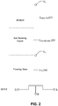
- FIG 2 is an illustration of a capacitance model of the microwell system depicted in Figure 1 . That is, the path from the analyte in microwell 101 to floating gate structure 118 can be modeled as a series connection of three capacitances: (1) the capacitance attributable to the analyte/ion-sensing layer interface (C ANALYTE 210); (2) the capacitance due to ion-sensing layer 116 (C ION-SENSING 220); and, (3) the oxide capacitance of floating gate structure 118 (C FG 230).
- C ANALYTE 210 the capacitance attributable to the analyte/ion-sensing layer interface
- C ION-SENSING 220 the capacitance due to ion-sensing layer 116
- C FG 230 oxide capacitance of floating gate structure 118
- capacitances in series form a capacitive voltage divider such that, in reference to Figure 2 , a fraction of voltage signal V S generated by or in the analyte is applied as a voltage signal V G that drives the ISFET.
- gate gain is defined as V G /V S
- unity gain is desirable such that the voltage generated by or in the analyte (e.g., V S ) is "fully" transferred to the floating gate of the ISFET (e.g., V G ).
- an output signal e.g., current
- FIG 3 is an illustration of an embodiment of a method 300 of fabricating a plurality of microwells for an array structure with a plurality of field effect transistors (FETs) such as, for example and without limitation, microwell array 102 and sensor array 105 of Figure 1 .
- FETs field effect transistors
- Each of the plurality of FETs has a gate structure such as, for example and without limitation, floating gate structure 118 of Figure 1 .
- the array structure can include a plurality of ISFETs, where each of the ISFETs has a floating gate structure.
- an ISFET with a floating gate structure is used in the description of method 300.
- the method 300 can be applied to other types of transistors with other types of gate structures and is not limited to ISFETs with a floating gate structure.
- An array structure with a plurality of ISFETs can be formed on a substrate using known fabrication methods and processes. For instance, conventional CMOS fabrication processes can be used to form the ISFET array, where a polysilicon gate is connected to metal layers to form a floating gate structure.
- a titanium nitride (TiN) layer is disposed on at least one conductive layer coupled to a floating gate structure of at least one ISFET in the array structure.
- a conductive layer can be coupled to a top surface of the floating gate structure (e.g., sensor plate 120 of Figure 1 ) to provide an electrically-conductive pathway between an ISFET and its respective microwell.
- a TiN layer can be disposed on the conductive layer using known fabrication methods and techniques.
- a insulation layer is disposed on the array structure.
- the insulation layer lies above the TiN layer of step 310.
- the insulation layer in step 320, can consist of multiple layers consisting of silicon nitride (Si 3 N 4 ) or silicon dioxide (SiO 2 ), according to an embodiment of the present invention.
- the insulation layer can be deposited using, for example and without limitation, atomic layer deposition.
- the thickness of the insulation layer can be in the range of 1.2-1.4 ⁇ m.
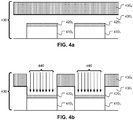
- Figure 4a is an illustration of two conductive layers 410 0 and 410 1 that are associated with the floating gate structures of two ISFETs (not shown). TiN layers 420 0 and 420 1 are disposed on conductive layers 410 0 and 410 1 , respectively.
- the TiN layers 4200 and 4201 can have a thickness in a range of 1 nm to 500 nm, such as a range of 1 nm to 250 nm, a range of 1 nm to 150 nm, a range of 1 nm to 100 nm, a range of 1 nm to 65 nm, a range of 5 nm to 50 nm, a range of 10 nm to 45 nm, or a range of 15 nm to 30 nm.
- 1 nm to 500 nm such as a range of 1 nm to 250 nm, a range of 1 nm to 150 nm, a range of 1 nm to 100 nm, a range of 1 nm to 65 nm, a range of 5 nm to 50 nm, a range of 10 nm to 45 nm, or a range of 15 nm to 30 nm.
- insulation layer 430 is disposed on TiN layers 420 0 and 420 1 and also surrounds conductive layers 410 0 and 410 1 .
- Insulation layer 430 can include one or more layers. As illustrated, the insulation layer 430 includes two layers: one layer of silicon nitride 430 0 and one layer of silicon dioxide 430 1 .
- the insulation layer 430 can have more or less than two layers, in which each of the layers can vary in thickness.
- the volume, shape, aspect ratio (such as base width-to-well depth ratio), and other dimensional characteristics of a microwell formed by insulation layer 430 (e.g., sidewalls of microwell) and TiN layers 420 0 and 420 1 (e.g., bottom surface of microwell) can have a variety of values.
- an opening above the floating gate structure of the at least one ISFET is formed by removing the insulation layer above the gate structure.
- the TiN layer is exposed and forms a bottom surface of a microwell.
- an etching process provides the opening above the gate structure such that the insulation layer is removed and the TiN layer is exposed.
- a resist can be applied over insulation layer 430 (not shown), a pattern can be implemented in the resist using lithography, and portions of the insulation layer can be etched in accordance with the pattern, and any remaining resist can be stripped.
- the result of the etching process is exposure of TiN layers 420 0 and 420 1 .
- Etching can include a wet etch or a plasma etch.
- the etching process can include plasma etching with fluorinated species such as, for example and without limitation, trifluoromethane, tetrafluoromethane, nitrogen fluoride, sulfur hexafluoride, or a combination thereof.
- the spectral frequency of the plasma in the etch chamber can be monitored to detect when the etching process reaches a transition between different layers of the insulation layer (e.g., for a multi-layer insulation layer) and between the insulation layer and the TiN layer.
- the plasma etch process can be monitored such that TiN layers 420 0 and 420 1 are not removed during the etch process. That is, the spectral frequency of the plasma is different between insulation layers 430 0 and 430 1 and between insulation layer 430 1 and TiN layers 420 0 and 420 1 .
- the progress of the etching process can be assessed by monitoring the differences in spectral frequency between these various layers, according to an embodiment of the present invention.
- the etch process is indicated by arrows 440.
- the power level of the plasma etcher can be adjusted during the etch process.
- the power level of the plasma etcher can be at a higher level during the etching of insulation layer 430 0 (e.g., 300 W) than during the etching of insulation layer 430 1 (e.g., 100 W).
- the differences in the spectral frequency between insulation layers 430 0 and 430 1 and between insulation layer 430 1 and TiN layers 420 0 and 420 1 can be closely monitored such that the etch process does not remove the TiN layer.
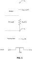
- FIG. 4b is an illustration of a capacitance model of the microwell system depicted in Figure 4b .
- the capacitance model of Figure 5 does not include C ION-SENSING 220. Rather, the TiN layer forms an ohmic contact R TIN 510 between C ANALYTE 210 and C FG 230.
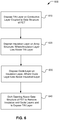
- Figure 6 is an illustration of another embodiment of a method 600 of fabricating a plurality of microwells for an array structure. Similar to method 300 of Figure 3 , method 600 provides a method of fabricating a plurality of microwells for an array structure with a plurality of field effect transistors (FETs) such as, for example and without limitation, microwell array 102 and sensor array 105 of Figure 1 . Each of the plurality of FETs has a gate structure such as, for example and without limitation, floating gate structure 118 of Figure 1 .
- the array structure can include a plurality of ISFETs, where each of the ISFETs has a floating gate structure.
- an ISFET with a floating gate structure is used in the description of method 600.
- the method 600 can be applied to other types of transistors with other types of gate structures and is not limited to ISFETs with a floating gate structure.
- Steps 610 and 620 of Figure 6 are similar to steps 310 and 320 of Figure 3 , respectively, described above.
- an oxide layer is disposed on the insulation layer (from step 620).
- the oxide layer lies above the insulation layer and the TiN layer.
- the oxide layer can be a tetra-ethyl-ortho-silicate (TEOS) that is deposited using a chemical vapor deposition process.
- TEOS tetra-ethyl-ortho-silicate
- Figure 7a is an illustration of an oxide layer 710 disposed on insulation layer 430.
- Insulation layer 430 (including sub-layers 430 0 and 430 1 ), TiN layers 420 0 and 420 1 , and conductive layers 410 0 and 410 0 are described above with regard to Figure 4 .
- the oxide layer 710 can vary in thickness.
- the volume, shape, aspect ratio (such as base width-to-well depth ratio), and other dimensional characteristics of a microwell formed by insulation layer 430 and oxide layer 710 (e.g., sidewalls of microwell) and TiN layers 420 0 and 420 1 (e.g., bottom surface of microwell) can depend on a particular application, including the nature of the reaction taking place, as well as the reagents, byproducts, and labeling techniques (if any) that are employed.
- an opening above the floating gate structure of the at least one ISFET is formed by removing the insulation layer and oxide layer above the gate structure.
- the TiN layer is exposed and forms a bottom surface of a microwell.
- an etching process provides the opening above the gate structure such that the insulation layer and oxide layer are removed and the TiN layer is exposed.
- a similar etch process as described above, with regard to step 330 of Figure 3 can be used in step 640.
- Figure 7b is an illustration of two microwells formed above conductive layers 410 0 and 410 1 , where TiN layers 420 0 and 420 1 form a bottom surface of the microwells.
- the etch process is indicated by arrows 720.
- the capacitance model of the microwell structure depicted in Figure 7b can also be depicted by the capacitor network of Figure 5 .
- a higher fraction of voltage signal V S generated by or in the analyte is applied as a voltage signal V G that drives the ISFET.
- higher sensitivity measurements can be obtained from an output signal (e.g., current) of the ISFET.
- FIG 8 is an illustration of an embodiment of a sensor device 800 with an ISFET array 810.
- ISFET array 810 includes a microwell array (e.g., microwell array 102 of Figure 1 ) and an associated sensor located beneath each microwell (e.g., sensor 114 of Figure 1 ).
- the combination of the microwell (e.g., microwell 101 of Figure 1 ) and associated sensor (e.g., sensor 114 of Figure 1 ) will be referred to as a "sensor pixel.”
- the microwell array in ISFET array 810 can be fabricated using the steps described in method 300 of Figure 3 and method 600 of Figure 6 , according to an embodiment of the present invention.
- Sensor device 800 also includes column circuits 820 and 850, row circuits 830 and 840, and input/output (I/O) pins 860.
- Column circuits 820 and 850 and row circuits 830 and 840 are configured to individually access and read out a particular sensor pixel from ISFET array 810.
- ISFET array 810 can include more than 1 million sensor pixels arranged in a row and column format, such that a particular sensor pixel can be individually accessed and read out using column circuits 820 and 850 and row circuits 830 and 840.
- Example column and row circuits and methods for accessing ISFET array 810 are described, for example, in U.S. Patent No.
- ISFET array 810 can be more or less than 1 million sensor pixels.
- I/O pins 260 are configured to provide the read out data to an external system or device for further processing.
- a sensor array including TiN channel sensors disposed over the gate structures of the sensors is exposed to a wash solution for a period of 6 hours. Images and histograms are collected from the sensor array before and after soaking in the wash solution.
- a sensor array is formed that includes TiN channel sensors disposed over gate structures as illustrated in Figure 11 , which includes an SEM image of two wells and the associated TiN layers deposited over metal sensor pads.
- Images and histograms are collected prior to exposure to the wash solution.
- a buffered solution flows over the sensor array for 30 minutes.
- An image ( Figure 9A ) and histogram ( Figure 10A ) are acquired.
- the image and histogram illustrate a uniform coverage of the TiN within the micowells.
- the sensor array is exposed to the wash solution for 6 hours.
- the wash solution is an aqueous solution including 100mM KCL, 8mM MgC12, 0.01% Triton-X 100, and 5uM EDTA and having a pH of 7.7.
- an image Figure 9B
- histogram Figure 10B
- the image retains significant uniformity.
- the histogram of Figure 10B only a slight shift in peak and width of distribution are found, indicating continued functionality of the TiN layer.
- the terms “comprises,” “comprising,” “includes,” “including,” “has,” “having” or any other variation thereof, are intended to cover a non-exclusive inclusion.
- a process, method, article, or apparatus that comprises a list of features is not necessarily limited only to those features but may include other features not expressly listed or inherent to such process, method, article, or apparatus.
- “or” refers to an inclusive-or and not to an exclusive-or. For example, a condition A or B is satisfied by any one of the following: A is true (or present) and B is false (or not present), A is false (or not present) and B is true (or present), and both A and B are true (or present).
Landscapes
- Health & Medical Sciences (AREA)
- Chemical & Material Sciences (AREA)
- Life Sciences & Earth Sciences (AREA)
- Physics & Mathematics (AREA)
- Molecular Biology (AREA)
- Analytical Chemistry (AREA)
- General Health & Medical Sciences (AREA)
- Chemical Kinetics & Catalysis (AREA)
- Hematology (AREA)
- Clinical Laboratory Science (AREA)
- Dispersion Chemistry (AREA)
- Spectroscopy & Molecular Physics (AREA)
- Engineering & Computer Science (AREA)
- Microelectronics & Electronic Packaging (AREA)
- Electrochemistry (AREA)
- Biochemistry (AREA)
- General Physics & Mathematics (AREA)
- Immunology (AREA)
- Pathology (AREA)
- Investigating Or Analyzing Materials By The Use Of Electric Means (AREA)
- Apparatus Associated With Microorganisms And Enzymes (AREA)
Claims (12)
- Procédé (300) de fabrication d'un micropuits pour une structure de réseau de capteurs, le procédé (300) comprenant :la disposition (310) d'une couche de nitrure de titane (TiN) (4200, 4201) sur au moins une couche conductrice (4100, 4101) disposée sur une structure de grille (118) d'au moins un transistor à effet de champ (FET) dans la structure de réseau de capteurs, la structure de réseau de capteurs comprenant plusieurs transistors à effet de champ, chacun de la pluralité des transistors à effet de champ ayant une structure de grille associée (118) et la couche de TiN (4200, 4201) étant située au-dessus d'un canal de conduction formé par une source et un drain de l'au moins un transistor à effet de champ, la structure de grille (118) se trouvant au-dessus du canal de conduction ;la disposition (320) d'une couche d'isolation (430) sur la structure de réseau de capteurs, la couche d'isolation (430) se trouvant au-dessus de la couche de TiN (4200, 4201) ; etla gravure (330) d'une ouverture au-dessus de la structure de grille (118) de l'au moins un transistor à effet de champ de façon à retirer la couche d'isolation (430) au-dessus de la structure de grille (118) et à exposer la couche de TiN (4200, 4201), la couche d'isolation (430) formant au moins une paroi latérale et la couche de TiN (4200, 4201) formant une surface inférieure du micropuits (101).
- Procédé (300) selon la revendication 1, dans lequel chacun de la pluralité de transistors à effet de champ est un transistor à effet de champ sensible aux ions (ISFET) comportant une structure de grille flottante (118), et dans lequel la disposition (310) de la couche de TiN (4200, 4201) consiste à disposer la couche de TiN (4200, 4201) sur une couche conductrice (4100, 4101) couplée à la structure de grille flottante (118).
- Procédé (300) selon la revendication 1, dans lequel la couche d'isolation (430) comprend au moins une couche de nitrure de silicium et au moins une couche de dioxyde de silicium, et dans lequel la gravure (330) consiste à enlever les couches de nitrure de silicium et de dioxyde de silicium au-dessus de la structure de grille (118) de façon à exposer la couche de TiN (4200, 4201).
- Procédé (300) selon la revendication 1, dans lequel la gravure de l'ouverture au-dessus de la structure de grille (118) consiste à graver (330) l'ouverture au moyen d'une gravure au plasma, dans lequel un niveau de puissance de la gravure au plasma est ajusté pendant la gravure de la couche d'isolation (430).
- Procédé (300) selon la revendication 4, dans lequel la couche d'isolation (430) comprend une couche supérieure de nitrure de silicium et une couche inférieure de dioxyde de silicium, et dans lequel la gravure (330) de l'ouverture au moyen de la gravure au plasma consiste à abaisser le niveau de puissance de la gravure au plasma après que la couche supérieure de nitrure de silicium est gravée.
- Procédé (300) selon la revendication 5, dans lequel l'abaissement du niveau de puissance de la gravure au plasma consiste à surveiller une fréquence spectrale de la gravure au plasma entre la couche supérieure de nitrure de silicium et la couche inférieure de dioxyde de silicium, et entre la couche inférieure de dioxyde de silicium et la couche de TiN (4200, 4201).
- Procédé (300) selon la revendication 1, comprenant en outre :après la disposition (320) de la couche d'isolation (430), la disposition d'une couche d'oxyde sur la couche d'isolation (430), la couche d'oxyde se trouvant au-dessus de la couche d'isolation (430) et de la couche de TiN (4200, 4201) ; etla gravure (330) de l'ouverture au-dessus de la structure de grille (118) de l'au moins un transistor à effet de champ, pour enlever les couches d'isolation et d'oxyde au-dessus de la structure de grille (118) et pour exposer la couche de TiN (4200, 4201), les couches isolantes et d'oxyde formant l'au moins une paroi latérale.
- Procédé (300) selon la revendication 7, dans lequel la gravure (330) de l'ouverture au-dessus de la structure de grille (118) consiste à enlever les couches d'isolation et d'oxyde au-dessus de la structure de grille (118) de façon à exposer la couche de TiN (4200, 4201).
- Réseau de capteurs (105) comprenant :une pluralité de transistors à effet de champ (FET), au moins un transistor à effet de champ comprenant une structure de grille (118) comportant une couche conductrice (4100, 4101) disposée au-dessus de celle-ci ; etune pluralité de micropuits (101) couplés à la pluralité de transistors à effet de champ, au moins un micropuits (101) comprenant au moins une paroi latérale formée d'une couche d'isolation (430) et/ou d'une couche d'oxyde et une surface inférieure formée d'une couche de nitrure de titane (TiN) (4200, 4201), la couche de TiN (4200, 4201) étant disposée sur la couche conductrice (4100, 4101), la couche de TiN (4200, 4201) étant située au-dessus d'un canal de conduction formé par une source et un drain du transistor à effet de champ, la structure à grille (118) se trouvant au-dessus du canal de conduction.
- Réseau de capteurs (105) selon la revendication 9, dans lequel la couche d'isolation (430) comprend au moins une couche de nitrure de silicium et au moins une couche de dioxyde de silicium.
- Réseau de capteurs (105) selon la revendication 9, dans lequel l'au moins un transistor à effet de champ est un transistor à effet de champ sensible aux ions (ISFET) comportant une structure de grille flottante (118).
- Réseau de capteurs (105) selon la revendication 11, dans lequel la couche de TiN (4200, 4201) est en contact avec une couche conductrice (4100, 4101) couplée à la structure de grille flottante (118).
Applications Claiming Priority (2)
| Application Number | Priority Date | Filing Date | Title |
|---|---|---|---|
| US13/354,072 US8821798B2 (en) | 2012-01-19 | 2012-01-19 | Titanium nitride as sensing layer for microwell structure |
| PCT/US2013/022140 WO2013109886A1 (fr) | 2012-01-19 | 2013-01-18 | Réseau de capteurs isfet comprenant du nitrure de titane en tant que couche de détection, situé en partie inférieure de structure à micro-puits |
Publications (2)
| Publication Number | Publication Date |
|---|---|
| EP2807478A1 EP2807478A1 (fr) | 2014-12-03 |
| EP2807478B1 true EP2807478B1 (fr) | 2019-07-31 |
Family
ID=47633574
Family Applications (1)
| Application Number | Title | Priority Date | Filing Date |
|---|---|---|---|
| EP13702546.6A Active EP2807478B1 (fr) | 2012-01-19 | 2013-01-18 | Réseau de capteurs isfet comprenant du nitrure de titane en tant que couche de détection, situé en partie inférieure de structure à micro-puits |
Country Status (3)
| Country | Link |
|---|---|
| US (1) | US8821798B2 (fr) |
| EP (1) | EP2807478B1 (fr) |
| WO (1) | WO2013109886A1 (fr) |
Families Citing this family (45)
| Publication number | Priority date | Publication date | Assignee | Title |
|---|---|---|---|---|
| US8349167B2 (en) | 2006-12-14 | 2013-01-08 | Life Technologies Corporation | Methods and apparatus for detecting molecular interactions using FET arrays |
| US8262900B2 (en) | 2006-12-14 | 2012-09-11 | Life Technologies Corporation | Methods and apparatus for measuring analytes using large scale FET arrays |
| US11339430B2 (en) | 2007-07-10 | 2022-05-24 | Life Technologies Corporation | Methods and apparatus for measuring analytes using large scale FET arrays |
| GB2457851B (en) | 2006-12-14 | 2011-01-05 | Ion Torrent Systems Inc | Methods and apparatus for measuring analytes using large scale fet arrays |
| EP2307577B1 (fr) | 2008-06-25 | 2015-06-03 | Life Technologies Corporation | Procédés pour mesurer des substances à analyser à l'aide de réseaux fet à grande échelle |
| US20100301398A1 (en) | 2009-05-29 | 2010-12-02 | Ion Torrent Systems Incorporated | Methods and apparatus for measuring analytes |
| US20100137143A1 (en) | 2008-10-22 | 2010-06-03 | Ion Torrent Systems Incorporated | Methods and apparatus for measuring analytes |
| US8776573B2 (en) | 2009-05-29 | 2014-07-15 | Life Technologies Corporation | Methods and apparatus for measuring analytes |
| US20120261274A1 (en) | 2009-05-29 | 2012-10-18 | Life Technologies Corporation | Methods and apparatus for measuring analytes |
| EP2588850B1 (fr) | 2010-06-30 | 2016-12-28 | Life Technologies Corporation | Procédé de test à sec de réseaux d'isfet |
| TWI465716B (zh) | 2010-06-30 | 2014-12-21 | 生命技術公司 | 用於檢測及測量化學反應及化合物之電晶體電路 |
| EP2588851B1 (fr) | 2010-06-30 | 2016-12-21 | Life Technologies Corporation | Circuit d'accumulation de charge sensible aux ions et procédé associé |
| US11307166B2 (en) | 2010-07-01 | 2022-04-19 | Life Technologies Corporation | Column ADC |
| US8653567B2 (en) | 2010-07-03 | 2014-02-18 | Life Technologies Corporation | Chemically sensitive sensor with lightly doped drains |
| WO2012036679A1 (fr) | 2010-09-15 | 2012-03-22 | Life Technologies Corporation | Procédés et appareil de mesure d'analytes |
| US8685324B2 (en) | 2010-09-24 | 2014-04-01 | Life Technologies Corporation | Matched pair transistor circuits |
| US9970984B2 (en) | 2011-12-01 | 2018-05-15 | Life Technologies Corporation | Method and apparatus for identifying defects in a chemical sensor array |
| US8786331B2 (en) | 2012-05-29 | 2014-07-22 | Life Technologies Corporation | System for reducing noise in a chemical sensor array |
| GB2508582A (en) * | 2012-10-12 | 2014-06-11 | Dna Electronics Ltd | ISFET with Titanium Nitride layer |
| US9080968B2 (en) | 2013-01-04 | 2015-07-14 | Life Technologies Corporation | Methods and systems for point of use removal of sacrificial material |
| US9841398B2 (en) | 2013-01-08 | 2017-12-12 | Life Technologies Corporation | Methods for manufacturing well structures for low-noise chemical sensors |
| US8963216B2 (en) | 2013-03-13 | 2015-02-24 | Life Technologies Corporation | Chemical sensor with sidewall spacer sensor surface |
| EP2972279B1 (fr) | 2013-03-15 | 2021-10-06 | Life Technologies Corporation | Capteur chimique avec des surfaces de capteur continues |
| WO2014149779A1 (fr) | 2013-03-15 | 2014-09-25 | Life Technologies Corporation | Dispositif chimique à élément conducteur mince |
| CN105264366B (zh) | 2013-03-15 | 2019-04-16 | 生命科技公司 | 具有一致传感器表面区域的化学传感器 |
| US9994889B2 (en) * | 2013-03-15 | 2018-06-12 | Nri R&D Patent Licensing, Llc | Advanced microplate, microtiter, and microarray technologies with per-well fluidics, gas exchange, electronic sensors, and imaging for cell culture and other applications |
| US9835585B2 (en) | 2013-03-15 | 2017-12-05 | Life Technologies Corporation | Chemical sensor with protruded sensor surface |
| US9116117B2 (en) | 2013-03-15 | 2015-08-25 | Life Technologies Corporation | Chemical sensor with sidewall sensor surface |
| US20140336063A1 (en) | 2013-05-09 | 2014-11-13 | Life Technologies Corporation | Windowed Sequencing |
| US10458942B2 (en) | 2013-06-10 | 2019-10-29 | Life Technologies Corporation | Chemical sensor array having multiple sensors per well |
| US9310332B2 (en) * | 2013-11-14 | 2016-04-12 | Taiwan Semiconductor Manufacturing Company Limited | Semiconductor device and selective heating thereof |
| US20160054312A1 (en) | 2014-04-28 | 2016-02-25 | Nanomedical Diagnostics, Inc. | Chemically differentiated sensor array |
| US9873100B2 (en) | 2014-09-17 | 2018-01-23 | Taiwan Semiconductor Manufacturing Company, Ltd. | Integrated circuit having temperature-sensing device |
| US9618474B2 (en) | 2014-12-18 | 2017-04-11 | Edico Genome, Inc. | Graphene FET devices, systems, and methods of using the same for sequencing nucleic acids |
| US10006910B2 (en) | 2014-12-18 | 2018-06-26 | Agilome, Inc. | Chemically-sensitive field effect transistors, systems, and methods for manufacturing and using the same |
| US10077472B2 (en) | 2014-12-18 | 2018-09-18 | Life Technologies Corporation | High data rate integrated circuit with power management |
| US11782057B2 (en) | 2014-12-18 | 2023-10-10 | Cardea Bio, Inc. | Ic with graphene fet sensor array patterned in layers above circuitry formed in a silicon based cmos wafer |
| US12298301B2 (en) | 2014-12-18 | 2025-05-13 | Cardea Bio, Inc. | Chemically-sensitive field effect transistors, systems, and methods for manufacturing and using the same |
| KR102593647B1 (ko) | 2014-12-18 | 2023-10-26 | 라이프 테크놀로지스 코포레이션 | 트랜스미터 구성을 갖춘 높은 데이터율 집적 회로 |
| US11921112B2 (en) | 2014-12-18 | 2024-03-05 | Paragraf Usa Inc. | Chemically-sensitive field effect transistors, systems, and methods for manufacturing and using the same |
| US10020300B2 (en) | 2014-12-18 | 2018-07-10 | Agilome, Inc. | Graphene FET devices, systems, and methods of using the same for sequencing nucleic acids |
| WO2016100521A1 (fr) | 2014-12-18 | 2016-06-23 | Life Technologies Corporation | Procédé et appareil pour mesurer des analytes au moyen de réseaux de tec à grande échelle |
| CA2971589C (fr) | 2014-12-18 | 2021-09-28 | Edico Genome Corporation | Transistor a effet de champ chimiquement sensible |
| WO2017201081A1 (fr) * | 2016-05-16 | 2017-11-23 | Agilome, Inc. | Dispositifs à fet au graphène, systèmes et leurs méthodes d'utilisation pour le séquençage d'acides nucléiques |
| US10788446B1 (en) | 2019-04-09 | 2020-09-29 | International Business Machines Corporation | Ion-sensitive field-effect transistor with micro-pillar well to enhance sensitivity |
Citations (2)
| Publication number | Priority date | Publication date | Assignee | Title |
|---|---|---|---|---|
| US20040185591A1 (en) * | 2003-03-19 | 2004-09-23 | Hsiung Stephen S.K. | Method for fabricating a titanium nitride sensing membrane on an EGFET |
| US20100137143A1 (en) * | 2008-10-22 | 2010-06-03 | Ion Torrent Systems Incorporated | Methods and apparatus for measuring analytes |
Family Cites Families (293)
| Publication number | Priority date | Publication date | Assignee | Title |
|---|---|---|---|---|
| GB2096824A (en) | 1981-04-09 | 1982-10-20 | Sibbald Alastair | Chemically sensitive field effect transistor |
| DE3269784D1 (en) | 1981-05-15 | 1986-04-17 | Licentia Gmbh | Method for measuring ionic concentrations |
| US4411741A (en) | 1982-01-12 | 1983-10-25 | University Of Utah | Apparatus and method for measuring the concentration of components in fluids |
| NL8302964A (nl) | 1983-08-24 | 1985-03-18 | Cordis Europ | Inrichting voor het bepalen van de aktiviteit van een ion (pion) in een vloeistof. |
| NL8303792A (nl) | 1983-11-03 | 1985-06-03 | Cordis Europ | Inrichting voorzien van een op een isfet gebaseerd meetcircuit; voor toepassing in het meetcircuit geschikte isfet en werkwijze ter vervaardiging van een in het meetcircuit toe te passen isfet. |
| JPS60128345A (ja) | 1983-12-15 | 1985-07-09 | Olympus Optical Co Ltd | イオン濃度測定装置 |
| US4660063A (en) | 1985-03-18 | 1987-04-21 | General Electric Company | Immersion type ISFET |
| DE3513168A1 (de) | 1985-04-12 | 1986-10-16 | Thomas 8000 München Dandekar | Biosensor bestehend aus einem halbleiter auf silizium oder kohlenstoffbasis (elektronischer teil) und nukleinbasen (od. anderen biol. monomeren) |
| US4743954A (en) | 1985-06-07 | 1988-05-10 | University Of Utah | Integrated circuit for a chemical-selective sensor with voltage output |
| US4863849A (en) | 1985-07-18 | 1989-09-05 | New York Medical College | Automatable process for sequencing nucleotide |
| EP0213825A3 (fr) | 1985-08-22 | 1989-04-26 | Molecular Devices Corporation | Capacitance multiple chimiquement modulée |
| GB8522785D0 (en) | 1985-09-14 | 1985-10-16 | Emi Plc Thorn | Chemical-sensitive semiconductor device |
| US4822566A (en) | 1985-11-19 | 1989-04-18 | The Johns Hopkins University | Optimized capacitive sensor for chemical analysis and measurement |
| US4864229A (en) | 1986-05-03 | 1989-09-05 | Integrated Ionics, Inc. | Method and apparatus for testing chemical and ionic sensors |
| US4722830A (en) | 1986-05-05 | 1988-02-02 | General Electric Company | Automated multiple stream analysis system |
| US5113870A (en) | 1987-05-01 | 1992-05-19 | Rossenfeld Joel P | Method and apparatus for the analysis, display and classification of event related potentials by interpretation of P3 responses |
| WO1989007263A1 (fr) | 1988-02-08 | 1989-08-10 | I-Stat Corporation | Electrode en oxyde de metal |
| US4971903A (en) | 1988-03-25 | 1990-11-20 | Edward Hyman | Pyrophosphate-based method and apparatus for sequencing nucleic acids |
| US4874499A (en) | 1988-05-23 | 1989-10-17 | Massachusetts Institute Of Technology | Electrochemical microsensors and method of making such sensors |
| US5200051A (en) | 1988-11-14 | 1993-04-06 | I-Stat Corporation | Wholly microfabricated biosensors and process for the manufacture and use thereof |
| US4990974A (en) | 1989-03-02 | 1991-02-05 | Thunderbird Technologies, Inc. | Fermi threshold field effect transistor |
| DE68925897T2 (de) | 1989-04-28 | 1996-10-02 | Ibm | Gate-Array-Zelle, bestehend aus FET's von verschiedener und optimierter Grösse |
| US6919211B1 (en) | 1989-06-07 | 2005-07-19 | Affymetrix, Inc. | Polypeptide arrays |
| US5143854A (en) | 1989-06-07 | 1992-09-01 | Affymax Technologies N.V. | Large scale photolithographic solid phase synthesis of polypeptides and receptor binding screening thereof |
| US5110441A (en) | 1989-12-14 | 1992-05-05 | Monsanto Company | Solid state ph sensor |
| US5317407A (en) | 1991-03-11 | 1994-05-31 | General Electric Company | Fixed-pattern noise correction circuitry for solid-state imager |
| KR940010562B1 (ko) | 1991-09-06 | 1994-10-24 | 손병기 | Ta_2O_5수소이온 감지막을 갖는 감이온 전계효과 트랜지스터의 제조방법 |
| GB2278235B (en) | 1991-10-21 | 1996-05-08 | Holm Kennedy James W | Method and device for biochemical sensing |
| US5846708A (en) | 1991-11-19 | 1998-12-08 | Massachusetts Institiute Of Technology | Optical and electrical methods and apparatus for molecule detection |
| US5637469A (en) | 1992-05-01 | 1997-06-10 | Trustees Of The University Of Pennsylvania | Methods and apparatus for the detection of an analyte utilizing mesoscale flow systems |
| US5284566A (en) | 1993-01-04 | 1994-02-08 | Bacharach, Inc. | Electrochemical gas sensor with wraparound reference electrode |
| US5436149A (en) | 1993-02-19 | 1995-07-25 | Barnes; Wayne M. | Thermostable DNA polymerase with enhanced thermostability and enhanced length and efficiency of primer extension |
| WO1994026029A1 (fr) | 1993-04-26 | 1994-11-10 | Unifet Incorporated | Procede et appareil pour multiplexer des dispositifs ayant de longues constantes de temps thermiques |
| JP3413664B2 (ja) | 1993-08-12 | 2003-06-03 | ソニー株式会社 | 電荷転送装置 |
| US5965452A (en) | 1996-07-09 | 1999-10-12 | Nanogen, Inc. | Multiplexed active biologic array |
| US5414284A (en) | 1994-01-19 | 1995-05-09 | Baxter; Ronald D. | ESD Protection of ISFET sensors |
| US5439839A (en) | 1994-07-13 | 1995-08-08 | Winbond Electronics Corporation | Self-aligned source/drain MOS process |
| US6654505B2 (en) | 1994-10-13 | 2003-11-25 | Lynx Therapeutics, Inc. | System and apparatus for sequential processing of analytes |
| US5631704A (en) | 1994-10-14 | 1997-05-20 | Lucent Technologies, Inc. | Active pixel sensor and imaging system having differential mode |
| US5490971A (en) | 1994-10-25 | 1996-02-13 | Sippican, Inc. | Chemical detector |
| US5585069A (en) | 1994-11-10 | 1996-12-17 | David Sarnoff Research Center, Inc. | Partitioned microelectronic and fluidic device array for clinical diagnostics and chemical synthesis |
| DE19512117A1 (de) | 1995-04-04 | 1996-10-10 | Itt Ind Gmbh Deutsche | Meßeinrichtung |
| US5856174A (en) | 1995-06-29 | 1999-01-05 | Affymetrix, Inc. | Integrated nucleic acid diagnostic device |
| US5702964A (en) | 1995-10-17 | 1997-12-30 | Lg Semicon, Co., Ltd. | Method for forming a semiconductor device having a floating gate |
| GB9620209D0 (en) | 1996-09-27 | 1996-11-13 | Cemu Bioteknik Ab | Method of sequencing DNA |
| US5958703A (en) | 1996-12-03 | 1999-09-28 | Glaxo Group Limited | Use of modified tethers in screening compound libraries |
| IL129767A0 (en) | 1996-12-12 | 2000-02-29 | Prolume Ltd | Apparatus and method for detecting and identifying infectious agents |
| US6605428B2 (en) | 1996-12-20 | 2003-08-12 | Roche Diagnostics Gmbh | Method for the direct, exponential amplification and sequencing of DNA molecules and its application |
| DE19653439A1 (de) | 1996-12-20 | 1998-07-02 | Svante Dr Paeaebo | Verfahren zur direkten, exponentiellen Amplifikation und Sequenzierung von DNA Molekülen und dessen Anwendung |
| US20030215857A1 (en) | 1996-12-20 | 2003-11-20 | Roche Diagnostics Gmbh | Method for the direct, exponential amplification and sequencing of DNA molecules and its application |
| US5793230A (en) | 1997-02-26 | 1998-08-11 | Sandia Corporation | Sensor readout detector circuit |
| US6197557B1 (en) | 1997-03-05 | 2001-03-06 | The Regents Of The University Of Michigan | Compositions and methods for analysis of nucleic acids |
| US6327410B1 (en) | 1997-03-14 | 2001-12-04 | The Trustees Of Tufts College | Target analyte sensors utilizing Microspheres |
| US7622294B2 (en) | 1997-03-14 | 2009-11-24 | Trustees Of Tufts College | Methods for detecting target analytes and enzymatic reactions |
| US6391622B1 (en) | 1997-04-04 | 2002-05-21 | Caliper Technologies Corp. | Closed-loop biochemical analyzers |
| US6872527B2 (en) | 1997-04-16 | 2005-03-29 | Xtrana, Inc. | Nucleic acid archiving |
| US5911873A (en) | 1997-05-02 | 1999-06-15 | Rosemount Analytical Inc. | Apparatus and method for operating an ISFET at multiple drain currents and gate-source voltages allowing for diagnostics and control of isopotential points |
| US7220550B2 (en) | 1997-05-14 | 2007-05-22 | Keensense, Inc. | Molecular wire injection sensors |
| US6969488B2 (en) | 1998-05-22 | 2005-11-29 | Solexa, Inc. | System and apparatus for sequential processing of analytes |
| JP4294740B2 (ja) | 1997-05-23 | 2009-07-15 | ソレクサ・インコーポレイテッド | 分析物の系列的プロセシングのためのシステムおよび装置 |
| JP4231560B2 (ja) | 1997-05-29 | 2009-03-04 | 株式会社堀場製作所 | 化学量の分布の電気化学的測定方法および装置 |
| US6002299A (en) | 1997-06-10 | 1999-12-14 | Cirrus Logic, Inc. | High-order multipath operational amplifier with dynamic offset reduction, controlled saturation current limiting, and current feedback for enhanced conditional stability |
| FR2764702B1 (fr) | 1997-06-11 | 1999-09-03 | Lyon Ecole Centrale | Procede d'identification et/ou de dosage de substances biologiques, presentes dans un liquide conducteur, dispositif et capteur d'affinite utiles pour la mise en oeuvre de ce procede |
| US5923421A (en) | 1997-07-24 | 1999-07-13 | Lockheed Martin Energy Research Corporation | Chemical detection using calorimetric spectroscopy |
| US6465178B2 (en) | 1997-09-30 | 2002-10-15 | Surmodics, Inc. | Target molecule attachment to surfaces |
| US6485944B1 (en) | 1997-10-10 | 2002-11-26 | President And Fellows Of Harvard College | Replica amplification of nucleic acid arrays |
| US6511803B1 (en) | 1997-10-10 | 2003-01-28 | President And Fellows Of Harvard College | Replica amplification of nucleic acid arrays |
| JP2001519538A (ja) | 1997-10-10 | 2001-10-23 | プレジデント・アンド・フェローズ・オブ・ハーバード・カレッジ | 核酸アレイのレプリカ増幅 |
| KR100251528B1 (ko) | 1997-10-22 | 2000-04-15 | 김덕중 | 복수개의 센스 소오스 패드를 구비한 센스 전계효과 트랜지스터 |
| US6369737B1 (en) | 1997-10-30 | 2002-04-09 | The Board Of Trustees Of The Leland Stanford Junior University | Method and apparatus for converting a low dynamic range analog signal to a large dynamic range floating-point digital representation |
| US7090975B2 (en) | 1998-03-13 | 2006-08-15 | Promega Corporation | Pyrophosphorolysis and incorporation of nucleotide method for nucleic acid detection |
| JP4482228B2 (ja) | 1998-04-09 | 2010-06-16 | カリフォルニア・インスティテュート・オブ・テクノロジー | アナライト検出のための電子技術 |
| CA2330673C (fr) | 1998-05-01 | 2009-05-26 | Arizona Board Of Regents | Procede de determination de la sequence nucleotidique d'oligonucleotides et de molecules d'adn |
| US6780591B2 (en) | 1998-05-01 | 2004-08-24 | Arizona Board Of Regents | Method of determining the nucleotide sequence of oligonucleotides and DNA molecules |
| US7875440B2 (en) | 1998-05-01 | 2011-01-25 | Arizona Board Of Regents | Method of determining the nucleotide sequence of oligonucleotides and DNA molecules |
| EP1090293B2 (fr) | 1998-06-24 | 2019-01-23 | Illumina, Inc. | Décodage de détecteurs matricels à microspheres |
| US6195585B1 (en) | 1998-06-26 | 2001-02-27 | Advanced Bionics Corporation | Remote monitoring of implantable cochlear stimulator |
| JP4137239B2 (ja) | 1998-08-03 | 2008-08-20 | 株式会社堀場製作所 | Isfetアレイ |
| EP1055121A1 (fr) | 1998-12-11 | 2000-11-29 | Symyx Technologies, Inc. | Systeme utilisant un reseau de detecteurs et procede associe de caracterisation rapide de materiaux |
| WO2000036152A1 (fr) | 1998-12-14 | 2000-06-22 | Li-Cor, Inc. | Systeme et procede de sequençage d'acides nucleiques mono-moleculaires par synthese de polymerase |
| DE19857953C2 (de) | 1998-12-16 | 2001-02-15 | Conducta Endress & Hauser | Vorrichtung zum Messen der Konzentration von Ionen in einer Meßflüssigkeit |
| US6429027B1 (en) | 1998-12-28 | 2002-08-06 | Illumina, Inc. | Composite arrays utilizing microspheres |
| US6361671B1 (en) | 1999-01-11 | 2002-03-26 | The Regents Of The University Of California | Microfabricated capillary electrophoresis chip and method for simultaneously detecting multiple redox labels |
| GB9901475D0 (en) | 1999-01-22 | 1999-03-17 | Pyrosequencing Ab | A method of DNA sequencing |
| US20020150909A1 (en) | 1999-02-09 | 2002-10-17 | Stuelpnagel John R. | Automated information processing in randomly ordered arrays |
| EP1157431A1 (fr) | 1999-02-22 | 2001-11-28 | Yissum Research Development Company Of The Hebrew University Of Jerusalem | Dispositif electrique hybride a composants biologiques |
| ATE556149T1 (de) | 1999-02-23 | 2012-05-15 | Caliper Life Sciences Inc | Manipulation von mikropartikeln in mikrofluidischen systemen |
| US20050244870A1 (en) | 1999-04-20 | 2005-11-03 | Illumina, Inc. | Nucleic acid sequencing using microsphere arrays |
| US6355431B1 (en) | 1999-04-20 | 2002-03-12 | Illumina, Inc. | Detection of nucleic acid amplification reactions using bead arrays |
| US20030108867A1 (en) | 1999-04-20 | 2003-06-12 | Chee Mark S | Nucleic acid sequencing using microsphere arrays |
| US7097973B1 (en) | 1999-06-14 | 2006-08-29 | Alpha Mos | Method for monitoring molecular species within a medium |
| US6818395B1 (en) | 1999-06-28 | 2004-11-16 | California Institute Of Technology | Methods and apparatus for analyzing polynucleotide sequences |
| AU1325201A (en) | 1999-07-16 | 2001-02-05 | Board Of Regents, The University Of Texas System | Detection system based on an analyte reactive particle |
| US6459398B1 (en) | 1999-07-20 | 2002-10-01 | D.S.P.C. Technologies Ltd. | Pulse modulated digital to analog converter (DAC) |
| US6423536B1 (en) | 1999-08-02 | 2002-07-23 | Molecular Dynamics, Inc. | Low volume chemical and biochemical reaction system |
| US7211390B2 (en) | 1999-09-16 | 2007-05-01 | 454 Life Sciences Corporation | Method of sequencing a nucleic acid |
| US7244559B2 (en) | 1999-09-16 | 2007-07-17 | 454 Life Sciences Corporation | Method of sequencing a nucleic acid |
| US6274320B1 (en) | 1999-09-16 | 2001-08-14 | Curagen Corporation | Method of sequencing a nucleic acid |
| US7124221B1 (en) | 1999-10-19 | 2006-10-17 | Rambus Inc. | Low latency multi-level communication interface |
| GB9926956D0 (en) | 1999-11-13 | 2000-01-12 | Koninkl Philips Electronics Nv | Amplifier |
| US6518024B2 (en) | 1999-12-13 | 2003-02-11 | Motorola, Inc. | Electrochemical detection of single base extension |
| US20030148301A1 (en) | 1999-12-10 | 2003-08-07 | Toshiya Aono | Method of detecting nucleotide polymorphism |
| JP2001175340A (ja) | 1999-12-14 | 2001-06-29 | Matsushita Electric Ind Co Ltd | 電位発生回路 |
| ATE283579T1 (de) | 2000-02-14 | 2004-12-15 | Koninkl Philips Electronics Nv | Strom-spannungsumwandler mit steuerbarer verstärkung und signalverarbeitender schaltkreis mit einem solchen umwandler |
| WO2001061044A1 (fr) | 2000-02-15 | 2001-08-23 | Lynx Therapeutics, Inc. | Systeme d'analyse et d'affichage de donnees servant a effectuer le sequencement d'adn a base de ligation |
| ATE412774T1 (de) | 2000-02-16 | 2008-11-15 | Illumina Inc | Parallele genotypisierung mehrerer patientenproben |
| FR2805826B1 (fr) | 2000-03-01 | 2002-09-20 | Nucleica | Nouvelles puces a adn |
| DE60144142D1 (de) | 2000-03-02 | 2011-04-14 | Microchips Inc | Mikromechanische geräte und verfahren zur speicherung und zur selektiven exposition von chemikalien |
| JP3442338B2 (ja) | 2000-03-17 | 2003-09-02 | 株式会社日立製作所 | Dna分析装置、dna塩基配列決定装置、dna塩基配列決定方法、および反応モジュール |
| US8232582B2 (en) | 2000-04-24 | 2012-07-31 | Life Technologies Corporation | Ultra-fast nucleic acid sequencing device and a method for making and using the same |
| US7001792B2 (en) | 2000-04-24 | 2006-02-21 | Eagle Research & Development, Llc | Ultra-fast nucleic acid sequencing device and a method for making and using the same |
| US6413792B1 (en) | 2000-04-24 | 2002-07-02 | Eagle Research Development, Llc | Ultra-fast nucleic acid sequencing device and a method for making and using the same |
| US20020042388A1 (en) | 2001-05-01 | 2002-04-11 | Cooper Mark J. | Lyophilizable and enhanced compacted nucleic acids |
| US20020168678A1 (en) | 2000-06-07 | 2002-11-14 | Li-Cor, Inc. | Flowcell system for nucleic acid sequencing |
| US6482639B2 (en) | 2000-06-23 | 2002-11-19 | The United States Of America As Represented By The Secretary Of The Navy | Microelectronic device and method for label-free detection and quantification of biological and chemical molecules |
| ATE377093T1 (de) | 2000-07-07 | 2007-11-15 | Visigen Biotechnologies Inc | Sequenzbestimmung in echtzeit |
| US6611037B1 (en) | 2000-08-28 | 2003-08-26 | Micron Technology, Inc. | Multi-trench region for accumulation of photo-generated charge in a CMOS imager |
| US6939451B2 (en) | 2000-09-19 | 2005-09-06 | Aclara Biosciences, Inc. | Microfluidic chip having integrated electrodes |
| JP4361271B2 (ja) | 2000-10-10 | 2009-11-11 | バイオトローブ・インコーポレイテツド | アッセイ、合成、および保存用の器具、ならびに、その作製、使用、および操作の方法 |
| US6537881B1 (en) | 2000-10-16 | 2003-03-25 | Advanced Micro Devices, Inc. | Process for fabricating a non-volatile memory device |
| US6558626B1 (en) | 2000-10-17 | 2003-05-06 | Nomadics, Inc. | Vapor sensing instrument for ultra trace chemical detection |
| AU2002241803A1 (en) | 2000-10-20 | 2002-06-18 | The Board Of Trustees Of The Leland Stanford Junior University | Transient electrical signal based methods and devices for characterizing molecular interaction and/or motion in a sample |
| US6770472B2 (en) | 2000-11-17 | 2004-08-03 | The Board Of Trustees Of The Leland Stanford Junior University | Direct DNA sequencing with a transcription protein and a nanometer scale electrometer |
| ATE408140T1 (de) | 2000-12-11 | 2008-09-15 | Harvard College | Vorrichtung enthaltend nanosensoren zur ekennung eines analyten und verfahren zu ihrer herstellung |
| GB2370410A (en) | 2000-12-22 | 2002-06-26 | Seiko Epson Corp | Thin film transistor sensor |
| WO2002079514A1 (fr) | 2001-01-10 | 2002-10-10 | The Trustees Of Boston College | Reseaux de nanotubes de carbone a pont d'adn |
| JP4809983B2 (ja) | 2001-02-14 | 2011-11-09 | 明彦 谷岡 | 生体高分子とリガンドとの相互作用を検出する装置及びその方法 |
| EP1236804A1 (fr) | 2001-03-02 | 2002-09-04 | Boehringer Mannheim Gmbh | Méthode pour la détermination d'un acide nucléique utilisant un controle |
| GB0105831D0 (en) | 2001-03-09 | 2001-04-25 | Toumaz Technology Ltd | Method for dna sequencing utilising enzyme linked field effect transistors |
| US8114591B2 (en) | 2001-03-09 | 2012-02-14 | Dna Electronics Ltd. | Sensing apparatus and method |
| DE10111458B4 (de) | 2001-03-09 | 2008-09-11 | Siemens Ag | Analyseeinrichtung |
| JP2004523243A (ja) | 2001-03-12 | 2004-08-05 | カリフォルニア インスティチュート オブ テクノロジー | 非同期性塩基伸長によってポリヌクレオチド配列を分析するための方法および装置 |
| JP2002272463A (ja) | 2001-03-22 | 2002-09-24 | Olympus Optical Co Ltd | 一塩基多型の型を判定する方法 |
| US6418968B1 (en) | 2001-04-20 | 2002-07-16 | Nanostream, Inc. | Porous microfluidic valves |
| JP3883512B2 (ja) | 2001-04-23 | 2007-02-21 | 三星電子株式会社 | 微細流路の側壁に形成されたmosfetよりなる物質検出用チップ、これを含む物質検出装置、及び物質検出装置を利用した物質検出方法 |
| KR100442838B1 (ko) | 2001-12-11 | 2004-08-02 | 삼성전자주식회사 | 프로브의 고정화 검출방법 및 상기 프로브와 표적시료의결합정도 검출방법 |
| KR100455283B1 (ko) | 2001-04-23 | 2004-11-08 | 삼성전자주식회사 | 물질 유로의 측벽에 형성된 mosfet으로 이루어진물질 검출용 칩, 이를 포함하는 물질 검출 장치, 이의제조 방법 및 물질 검출 장치를 이용한 물질 검출 방법 |
| US20040023253A1 (en) | 2001-06-11 | 2004-02-05 | Sandeep Kunwar | Device structure for closely spaced electrodes |
| WO2003004690A2 (fr) | 2001-07-06 | 2003-01-16 | 454$m(3) CORPORATION | Methode utilisant un filtre poreux pour isoler en parallele des micro-reactions chimiques independantes |
| DE10133363A1 (de) | 2001-07-10 | 2003-01-30 | Infineon Technologies Ag | Messzelle und Messfeld mit solchen Messzellen sowie Verwendung einer Messzelle und Verwendung eines Messfeldes |
| US6929944B2 (en) | 2001-08-31 | 2005-08-16 | Beckman Coulter, Inc. | Analysis using a distributed sample |
| US20030054396A1 (en) | 2001-09-07 | 2003-03-20 | Weiner Michael P. | Enzymatic light amplification |
| DE10151021A1 (de) | 2001-10-16 | 2003-04-30 | Infineon Technologies Ag | Sensor-Anordnung |
| DE10151020A1 (de) | 2001-10-16 | 2003-04-30 | Infineon Technologies Ag | Schaltkreis-Anordnung, Sensor-Array und Biosensor-Array |
| US6795117B2 (en) | 2001-11-06 | 2004-09-21 | Candela Microsystems, Inc. | CMOS image sensor with noise cancellation |
| US20030124599A1 (en) | 2001-11-14 | 2003-07-03 | Shiping Chen | Biochemical analysis system with combinatorial chemistry applications |
| US7049645B2 (en) | 2001-11-16 | 2006-05-23 | Bio-X Inc. | FET type sensor, ion density detecting method comprising this sensor, and base sequence detecting method |
| US20050106587A1 (en) | 2001-12-21 | 2005-05-19 | Micronas Gmbh | Method for determining of nucleic acid analytes |
| US6518146B1 (en) | 2002-01-09 | 2003-02-11 | Motorola, Inc. | Semiconductor device structure and method for forming |
| US7772383B2 (en) | 2002-01-25 | 2010-08-10 | The Trustees Of Princeton University | Chemical PCR: Compositions for enhancing polynucleotide amplification reactions |
| KR100403637B1 (ko) | 2002-01-26 | 2003-10-30 | 삼성전자주식회사 | 출력 일그러짐을 최소화하는 파워 앰프 클리핑 회로 |
| US6614301B2 (en) | 2002-01-31 | 2003-09-02 | Intel Corporation | Differential amplifier offset adjustment |
| US7276749B2 (en) | 2002-02-05 | 2007-10-02 | E-Phocus, Inc. | Image sensor with microcrystalline germanium photodiode layer |
| US6926865B2 (en) | 2002-02-11 | 2005-08-09 | Matsushita Electric Industrial Co., Ltd. | Method and apparatus for detecting DNA hybridization |
| JP2003258128A (ja) | 2002-02-27 | 2003-09-12 | Nec Electronics Corp | 不揮発性半導体記憶装置およびその製造方法ならびにその動作方法 |
| US6953958B2 (en) | 2002-03-19 | 2005-10-11 | Cornell Research Foundation, Inc. | Electronic gain cell based charge sensor |
| US6828685B2 (en) | 2002-06-14 | 2004-12-07 | Hewlett-Packard Development Company, L.P. | Memory device having a semiconducting polymer film |
| US6894930B2 (en) | 2002-06-19 | 2005-05-17 | Sandisk Corporation | Deep wordline trench to shield cross coupling between adjacent cells for scaled NAND |
| AU2003258969A1 (en) | 2002-06-27 | 2004-01-19 | Nanosys Inc. | Planar nanowire based sensor elements, devices, systems and methods for using and making same |
| US7092757B2 (en) | 2002-07-12 | 2006-08-15 | Cardiac Pacemakers, Inc. | Minute ventilation sensor with dynamically adjusted excitation current |
| US6885827B2 (en) | 2002-07-30 | 2005-04-26 | Amplification Technologies, Inc. | High sensitivity, high resolution detection of signals |
| US7842377B2 (en) | 2003-08-08 | 2010-11-30 | Boston Scientific Scimed, Inc. | Porous polymeric particle comprising polyvinyl alcohol and having interior to surface porosity-gradient |
| JP3980030B2 (ja) | 2002-08-12 | 2007-09-19 | 株式会社日立ハイテクノロジーズ | Dnaマイクロアレイを用いた核酸検出方法及び核酸検出装置 |
| US7267751B2 (en) | 2002-08-20 | 2007-09-11 | Nanogen, Inc. | Programmable multiplexed active biologic array |
| GB0219541D0 (en) | 2002-08-22 | 2002-10-02 | Secr Defence | Method and apparatus for stand-off chemical detection |
| US8449824B2 (en) | 2002-09-09 | 2013-05-28 | Yizhong Sun | Sensor instrument system including method for detecting analytes in fluids |
| US7595883B1 (en) | 2002-09-16 | 2009-09-29 | The Board Of Trustees Of The Leland Stanford Junior University | Biological analysis arrangement and approach therefor |
| SE0202867D0 (sv) | 2002-09-27 | 2002-09-27 | Pyrosequencing Ab | New sequencing method |
| CN1500887A (zh) | 2002-10-01 | 2004-06-02 | ���µ�����ҵ��ʽ���� | 引物伸长反应检测方法、碱基种类判别方法及其装置 |
| WO2004034025A2 (fr) | 2002-10-10 | 2004-04-22 | Nanosys, Inc. | Biocapteurs sur transistors a effet de champ a nanostructure chimique |
| US20040079636A1 (en) | 2002-10-25 | 2004-04-29 | Chin Hsia | Biomedical ion sensitive semiconductor sensor and sensor array |
| US7053439B2 (en) | 2002-10-29 | 2006-05-30 | Edwin Kan | Chemoreceptive semiconductor structure |
| US6700814B1 (en) | 2002-10-30 | 2004-03-02 | Motorola, Inc. | Sense amplifier bias circuit for a memory having at least two distinct resistance states |
| DE10251757B4 (de) | 2002-11-05 | 2006-03-09 | Micronas Holding Gmbh | Vorrichtung zur Bestimmung der Konzentration von in einer zu untersuchenden Probe enthaltenen Liganden |
| US7022288B1 (en) | 2002-11-13 | 2006-04-04 | The United States Of America As Represented By The Secretary Of The Navy | Chemical detection sensor system |
| US20040197803A1 (en) | 2002-12-06 | 2004-10-07 | Hidenobu Yaku | Method, primer and kit for determining base type |
| US7575865B2 (en) | 2003-01-29 | 2009-08-18 | 454 Life Sciences Corporation | Methods of amplifying and sequencing nucleic acids |
| CA2513899C (fr) | 2003-01-29 | 2013-03-26 | 454 Corporation | Procede d'amplification et de sequencage d'acides nucleiques |
| US20050006234A1 (en) | 2003-02-13 | 2005-01-13 | Arjang Hassibi | Semiconductor electrochemical bio-sensor array |
| US20070262363A1 (en) | 2003-02-28 | 2007-11-15 | Board Of Regents, University Of Texas System | Low temperature fabrication of discrete silicon-containing substrates and devices |
| US7291496B2 (en) | 2003-05-22 | 2007-11-06 | University Of Hawaii | Ultrasensitive biochemical sensor |
| US7250115B2 (en) | 2003-06-12 | 2007-07-31 | Agilent Technologies, Inc | Nanopore with resonant tunneling electrodes |
| JP2005077210A (ja) | 2003-08-29 | 2005-03-24 | National Institute For Materials Science | 生体分子検出素子及びそれを用いた核酸解析方法 |
| GB0322010D0 (en) | 2003-09-19 | 2003-10-22 | Univ Cambridge Tech | Detection of molecular interactions using field effect transistors |
| GB0323224D0 (en) | 2003-10-03 | 2003-11-05 | Rolls Royce Plc | A module for a fuel cell stack |
| US20070087401A1 (en) | 2003-10-17 | 2007-04-19 | Andy Neilson | Analysis of metabolic activity in cells using extracellular flux rate measurements |
| WO2005043160A2 (fr) | 2003-10-31 | 2005-05-12 | University Of Hawaii | Plate-forme de detection ultrasensible d'agents biochimiques |
| US7067886B2 (en) | 2003-11-04 | 2006-06-27 | International Business Machines Corporation | Method of assessing potential for charging damage in SOI designs and structures for eliminating potential for damage |
| US7981362B2 (en) | 2003-11-04 | 2011-07-19 | Meso Scale Technologies, Llc | Modular assay plates, reader systems and methods for test measurements |
| DE10352917A1 (de) | 2003-11-11 | 2005-06-16 | Endress + Hauser Conducta Gesellschaft für Mess- und Regeltechnik mbH + Co. KG | Sensoranordnung mit mehreren potentiometrischen Sensoren |
| US7169560B2 (en) | 2003-11-12 | 2007-01-30 | Helicos Biosciences Corporation | Short cycle methods for sequencing polynucleotides |
| US7279588B2 (en) | 2003-12-02 | 2007-10-09 | Seoul National University Foundation | Dinuclear metal complex and pyrophosphate assay using the same |
| US7462512B2 (en) | 2004-01-12 | 2008-12-09 | Polytechnic University | Floating gate field effect transistors for chemical and/or biological sensing |
| JP4065855B2 (ja) | 2004-01-21 | 2008-03-26 | 株式会社日立製作所 | 生体および化学試料検査装置 |
| US7927797B2 (en) | 2004-01-28 | 2011-04-19 | 454 Life Sciences Corporation | Nucleic acid amplification with continuous flow emulsion |
| JP3903183B2 (ja) | 2004-02-03 | 2007-04-11 | 独立行政法人物質・材料研究機構 | 遺伝子検出電界効果デバイスおよびこれを用いた遺伝子多型解析方法 |
| AU2005216549A1 (en) | 2004-02-27 | 2005-09-09 | President And Fellows Of Harvard College | Polony fluorescent in situ sequencing beads |
| US20060057604A1 (en) | 2004-03-15 | 2006-03-16 | Thinkfar Nanotechnology Corporation | Method for electrically detecting oligo-nucleotides with nano-particles |
| JP4127679B2 (ja) | 2004-03-18 | 2008-07-30 | 株式会社東芝 | 核酸検出カセット及び核酸検出装置 |
| DE102004014537A1 (de) | 2004-03-23 | 2005-10-13 | Fujitsu Ltd., Kawasaki | Chipintegrierter Detektor zum Analysieren von Flüssigkeiten |
| US20050221473A1 (en) | 2004-03-30 | 2005-10-06 | Intel Corporation | Sensor array integrated circuits |
| WO2005095938A1 (fr) | 2004-04-01 | 2005-10-13 | Nanyang Technological University | Microcircuit adressable a transistors pour la conduite d'essais |
| US7544979B2 (en) | 2004-04-16 | 2009-06-09 | Technion Research & Development Foundation Ltd. | Ion concentration transistor and dual-mode sensors |
| US7462452B2 (en) | 2004-04-30 | 2008-12-09 | Pacific Biosciences Of California, Inc. | Field-switch sequencing |
| TWI261801B (en) | 2004-05-24 | 2006-09-11 | Rohm Co Ltd | Organic EL drive circuit and organic EL display device using the same organic EL drive circuit |
| US7264934B2 (en) | 2004-06-10 | 2007-09-04 | Ge Healthcare Bio-Sciences Corp. | Rapid parallel nucleic acid analysis |
| US20060024711A1 (en) | 2004-07-02 | 2006-02-02 | Helicos Biosciences Corporation | Methods for nucleic acid amplification and sequence determination |
| GB2416210B (en) | 2004-07-13 | 2008-02-20 | Christofer Toumazou | Ion sensitive field effect transistors |
| JP3874772B2 (ja) | 2004-07-21 | 2007-01-31 | 株式会社日立製作所 | 生体関連物質測定装置及び測定方法 |
| JP4455215B2 (ja) | 2004-08-06 | 2010-04-21 | キヤノン株式会社 | 撮像装置 |
| US7190026B2 (en) | 2004-08-23 | 2007-03-13 | Enpirion, Inc. | Integrated circuit employable with a power converter |
| WO2006022370A1 (fr) | 2004-08-27 | 2006-03-02 | National Institute For Materials Science | Procédé d’analyse de séquence d’adn à l’aide d’un dispositif à effet de champ et analyseur de séquence de base |
| US20070212681A1 (en) | 2004-08-30 | 2007-09-13 | Benjamin Shapiro | Cell canaries for biochemical pathogen detection |
| US7609303B1 (en) | 2004-10-12 | 2009-10-27 | Melexis Tessenderlo Nv | Low noise active pixel image sensor using a modified reset value |
| US7534097B2 (en) | 2004-10-15 | 2009-05-19 | Nanyang Technological University | Method and apparatus for controlling multi-fluid flow in a micro channel |
| US7381936B2 (en) | 2004-10-29 | 2008-06-03 | Ess Technology, Inc. | Self-calibrating anti-blooming circuit for CMOS image sensor having a spillover protection performance in response to a spillover condition |
| US7785785B2 (en) | 2004-11-12 | 2010-08-31 | The Board Of Trustees Of The Leland Stanford Junior University | Charge perturbation detection system for DNA and other molecules |
| WO2006086034A2 (fr) | 2004-11-18 | 2006-08-17 | Morgan Research Corporation | Spectrophotometre miniature a transformee de fourier |
| US20060205061A1 (en) | 2004-11-24 | 2006-09-14 | California Institute Of Technology | Biosensors based upon actuated desorption |
| KR100623177B1 (ko) | 2005-01-25 | 2006-09-13 | 삼성전자주식회사 | 높은 유전율을 갖는 유전체 구조물, 이의 제조 방법, 이를포함하는 불휘발성 반도체 메모리 장치 및 그 제조 방법 |
| US7476504B2 (en) | 2005-01-31 | 2009-01-13 | Pacific Biosciences Of California, Inc. | Use of reversible extension terminator in nucleic acid sequencing |
| US9040237B2 (en) | 2005-03-04 | 2015-05-26 | Intel Corporation | Sensor arrays and nucleic acid sequencing applications |
| EP1870703B1 (fr) | 2005-03-11 | 2014-04-02 | National University Corporation Toyohashi University of Technology | Appareil cumulatif de détection des phénomènes chimiques ou physiques |
| CA2603576A1 (fr) | 2005-04-05 | 2006-10-19 | Protein Discovery, Inc. | Procedes et dispositifs ameliores de concentration et de fractionnement de substances a analyser aux fins d'analyse chimique, notamment par spectrometrie de masse (ms) a desorption-ionisation par impact laser assistee par matrice (maldi) |
| US20060228721A1 (en) | 2005-04-12 | 2006-10-12 | Leamon John H | Methods for determining sequence variants using ultra-deep sequencing |
| TWI287041B (en) | 2005-04-27 | 2007-09-21 | Jung-Tang Huang | An ultra-rapid DNA sequencing method with nano-transistors array based devices |
| US20060269927A1 (en) | 2005-05-25 | 2006-11-30 | Lieber Charles M | Nanoscale sensors |
| CN1881457A (zh) | 2005-06-14 | 2006-12-20 | 松下电器产业株式会社 | 致动器控制方法和使用该方法的盘装置 |
| EP3257949A1 (fr) | 2005-06-15 | 2017-12-20 | Complete Genomics Inc. | Analyse d'acide nucléique par des mélanges aléatoires de fragments non chevauchants |
| TW200701588A (en) | 2005-06-29 | 2007-01-01 | Leadtrend Tech Corp | Dual loop voltage regulation circuit of power supply chip |
| US7890891B2 (en) | 2005-07-11 | 2011-02-15 | Peregrine Semiconductor Corporation | Method and apparatus improving gate oxide reliability by controlling accumulated charge |
| JP2007035726A (ja) | 2005-07-22 | 2007-02-08 | Rohm Co Ltd | 半導体装置、モジュールおよび電子機器 |
| US7365597B2 (en) | 2005-08-19 | 2008-04-29 | Micron Technology, Inc. | Switched capacitor amplifier with higher gain and improved closed-loop gain accuracy |
| JP4353958B2 (ja) | 2005-09-15 | 2009-10-28 | 株式会社日立製作所 | Dna計測装置、及びdna計測方法 |
| US7466258B1 (en) | 2005-10-07 | 2008-12-16 | Cornell Research Foundation, Inc. | Asynchronous analog-to-digital converter and method |
| US7794584B2 (en) | 2005-10-12 | 2010-09-14 | The Research Foundation Of State University Of New York | pH-change sensor and method |
| US7335526B2 (en) | 2005-10-31 | 2008-02-26 | Hewlett-Packard Development Company, L.P. | Sensing system |
| TWI295729B (en) | 2005-11-01 | 2008-04-11 | Univ Nat Yunlin Sci & Tech | Preparation of a ph sensor, the prepared ph sensor, systems comprising the same, and measurement using the systems |
| US7538827B2 (en) | 2005-11-17 | 2009-05-26 | Chunghwa Picture Tubes, Ltd. | Pixel structure |
| US7576037B2 (en) | 2005-11-18 | 2009-08-18 | Mei Technologies, Inc. | Process and apparatus for combinatorial synthesis |
| GB2436619B (en) | 2005-12-19 | 2010-10-06 | Toumaz Technology Ltd | Sensor circuits |
| KR100718144B1 (ko) | 2006-01-09 | 2007-05-14 | 삼성전자주식회사 | 이온 물질 검출용 fet 기반 센서, 그를 포함하는 이온물질 검출 장치 및 그를 이용한 이온 물질 검출 방법 |
| US8017938B2 (en) | 2006-03-17 | 2011-09-13 | The United States Of America As Represented By The Department Of Health And Human Services | Apparatus for microarray binding sensors having biological probe materials using carbon nanotube transistors |
| US20070233477A1 (en) | 2006-03-30 | 2007-10-04 | Infima Ltd. | Lossless Data Compression Using Adaptive Context Modeling |
| US7923240B2 (en) | 2006-03-31 | 2011-04-12 | Intel Corporation | Photo-activated field effect transistor for bioanalyte detection |
| WO2007123908A2 (fr) | 2006-04-18 | 2007-11-01 | Advanced Liquid Logic, Inc. | Opérations en puits multiples à base de gouttelettes |
| KR100723426B1 (ko) | 2006-04-26 | 2007-05-30 | 삼성전자주식회사 | 이온 물질 검출용 전계 효과 트랜지스터 및 그를 이용한이온 물질 검출 방법 |
| EP2530167A1 (fr) | 2006-05-11 | 2012-12-05 | Raindance Technologies, Inc. | Dispositifs microfluidiques |
| JP4211805B2 (ja) | 2006-06-01 | 2009-01-21 | エプソンイメージングデバイス株式会社 | 電気光学装置および電子機器 |
| US8129978B2 (en) | 2006-07-13 | 2012-03-06 | National University Corporation Nagoya University | Material detector |
| KR100799577B1 (ko) | 2006-08-31 | 2008-01-30 | 한국전자통신연구원 | 가스 및 생화학물질 감지용 센서 제조 방법과 그 센서를포함하는 집적회로 및 그 제조 방법 |
| US8231831B2 (en) | 2006-10-06 | 2012-07-31 | Sharp Laboratories Of America, Inc. | Micro-pixelated fluid-assay structure |
| GB2457851B (en) | 2006-12-14 | 2011-01-05 | Ion Torrent Systems Inc | Methods and apparatus for measuring analytes using large scale fet arrays |
| US8349167B2 (en) | 2006-12-14 | 2013-01-08 | Life Technologies Corporation | Methods and apparatus for detecting molecular interactions using FET arrays |
| US8262900B2 (en) | 2006-12-14 | 2012-09-11 | Life Technologies Corporation | Methods and apparatus for measuring analytes using large scale FET arrays |
| US7972828B2 (en) | 2006-12-19 | 2011-07-05 | Sigma-Aldrich Co. | Stabilized compositions of thermostable DNA polymerase and anionic or zwitterionic detergent |
| US7932034B2 (en) | 2006-12-20 | 2011-04-26 | The Board Of Trustees Of The Leland Stanford Junior University | Heat and pH measurement for sequencing of DNA |
| WO2008089282A2 (fr) | 2007-01-16 | 2008-07-24 | Silver James H | Capteurs destinés à détecter des substances indicatives d'accident vasculaire cérébral, d'ischémie, d'infection ou d'inflammation |
| JP4325684B2 (ja) | 2007-02-20 | 2009-09-02 | 株式会社デンソー | センサ制御装置、及び印加電圧特性の調整方法 |
| JP5368321B2 (ja) | 2007-03-02 | 2013-12-18 | ディ・エヌ・エイ・エレクトロニクス・リミテッド | 固相pH検出を用いたqPCR |
| EP1975246A1 (fr) | 2007-03-29 | 2008-10-01 | Micronas Holding GmbH | Séquençage sans marquage sur une surface solide en utilisant un transitor à effet de champ |
| BRPI0813718A2 (pt) | 2007-07-13 | 2014-12-30 | Univ Leland Stanford Junior | Método e aparelho que utilizam um campo elétrico para ensaios biológicos aperfeiçoados |
| US7609093B2 (en) | 2007-08-03 | 2009-10-27 | Tower Semiconductor Ltd. | Comparator with low supply current spike and input offset cancellation |
| JP2010537643A (ja) | 2007-08-29 | 2010-12-09 | アプライド バイオシステムズ, エルエルシー | 代替的な核酸配列決定法 |
| KR100940415B1 (ko) | 2007-12-03 | 2010-02-02 | 주식회사 동부하이텍 | 배면 드레인 구조 웨이퍼의 온저항 측정방법 |
| US20100273166A1 (en) | 2007-12-13 | 2010-10-28 | Nxp B.V. | biosensor device and method of sequencing biological particles |
| US8124936B1 (en) | 2007-12-13 | 2012-02-28 | The United States Of America As Represented By The Secretary Of The Army | Stand-off chemical detector |
| EP2224230B1 (fr) | 2007-12-20 | 2019-03-20 | National University Corporation Toyohashi University of Technology | Détecteur combiné |
| US20090194416A1 (en) | 2008-01-31 | 2009-08-06 | Chung Yuan Christian University | Potentiometric biosensor for detection of creatinine and forming method thereof |
| DE102008012899A1 (de) | 2008-03-06 | 2009-09-10 | Robert Bosch Gmbh | Verfahren zum Betreiben eines Gassensors |
| US8067731B2 (en) | 2008-03-08 | 2011-11-29 | Scott Technologies, Inc. | Chemical detection method and system |
| US7885490B2 (en) | 2008-03-10 | 2011-02-08 | Octrolix Bv | Optical chemical detector and method |
| US7667501B2 (en) | 2008-03-19 | 2010-02-23 | Texas Instruments Incorporated | Correlated double sampling technique |
| US7821806B2 (en) | 2008-06-18 | 2010-10-26 | Nscore Inc. | Nonvolatile semiconductor memory circuit utilizing a MIS transistor as a memory cell |
| GB2461127B (en) | 2008-06-25 | 2010-07-14 | Ion Torrent Systems Inc | Methods and apparatus for measuring analytes using large scale FET arrays |
| EP2307577B1 (fr) | 2008-06-25 | 2015-06-03 | Life Technologies Corporation | Procédés pour mesurer des substances à analyser à l'aide de réseaux fet à grande échelle |
| KR101026468B1 (ko) | 2008-09-10 | 2011-04-01 | 한국전자통신연구원 | 생분자 검출 장치 및 검출 방법 |
| US20100301398A1 (en) | 2009-05-29 | 2010-12-02 | Ion Torrent Systems Incorporated | Methods and apparatus for measuring analytes |
| CN103901090B (zh) | 2008-10-22 | 2017-03-22 | 生命技术公司 | 用于生物和化学分析的集成式传感器阵列 |
| US7898277B2 (en) | 2008-12-24 | 2011-03-01 | Agere Systems Inc. | Hot-electronic injection testing of transistors on a wafer |
| US8101479B2 (en) | 2009-03-27 | 2012-01-24 | National Semiconductor Corporation | Fabrication of asymmetric field-effect transistors using L-shaped spacers |
| US8673627B2 (en) | 2009-05-29 | 2014-03-18 | Life Technologies Corporation | Apparatus and methods for performing electrochemical reactions |
| US20120261274A1 (en) | 2009-05-29 | 2012-10-18 | Life Technologies Corporation | Methods and apparatus for measuring analytes |
| US8776573B2 (en) | 2009-05-29 | 2014-07-15 | Life Technologies Corporation | Methods and apparatus for measuring analytes |
| US20110037121A1 (en) | 2009-08-16 | 2011-02-17 | Tung-Hsing Lee | Input/output electrostatic discharge device with reduced junction breakdown voltage |
| SG188863A1 (en) | 2009-09-11 | 2013-04-30 | Agency Science Tech & Res | Method of determining a sensitivity of a biosensor arrangement, and biosensor sensitivity determining system |
| US8545248B2 (en) | 2010-01-07 | 2013-10-01 | Life Technologies Corporation | System to control fluid flow based on a leak detected by a sensor |
| US9088208B2 (en) | 2010-01-27 | 2015-07-21 | Intersil Americas LLC | System and method for high precision current sensing |
| EP2588850B1 (fr) | 2010-06-30 | 2016-12-28 | Life Technologies Corporation | Procédé de test à sec de réseaux d'isfet |
| TWI465716B (zh) | 2010-06-30 | 2014-12-21 | 生命技術公司 | 用於檢測及測量化學反應及化合物之電晶體電路 |
| EP2588851B1 (fr) | 2010-06-30 | 2016-12-21 | Life Technologies Corporation | Circuit d'accumulation de charge sensible aux ions et procédé associé |
| US8653567B2 (en) | 2010-07-03 | 2014-02-18 | Life Technologies Corporation | Chemically sensitive sensor with lightly doped drains |
| US10241075B2 (en) | 2010-12-30 | 2019-03-26 | Life Technologies Corporation | Methods, systems, and computer readable media for nucleic acid sequencing |
-
2012
- 2012-01-19 US US13/354,072 patent/US8821798B2/en active Active
-
2013
- 2013-01-18 WO PCT/US2013/022140 patent/WO2013109886A1/fr not_active Ceased
- 2013-01-18 EP EP13702546.6A patent/EP2807478B1/fr active Active
Patent Citations (2)
| Publication number | Priority date | Publication date | Assignee | Title |
|---|---|---|---|---|
| US20040185591A1 (en) * | 2003-03-19 | 2004-09-23 | Hsiung Stephen S.K. | Method for fabricating a titanium nitride sensing membrane on an EGFET |
| US20100137143A1 (en) * | 2008-10-22 | 2010-06-03 | Ion Torrent Systems Incorporated | Methods and apparatus for measuring analytes |
Also Published As
| Publication number | Publication date |
|---|---|
| WO2013109886A1 (fr) | 2013-07-25 |
| WO2013109886A8 (fr) | 2014-02-27 |
| US20130190211A1 (en) | 2013-07-25 |
| US8821798B2 (en) | 2014-09-02 |
| EP2807478A1 (fr) | 2014-12-03 |
Similar Documents
| Publication | Publication Date | Title |
|---|---|---|
| EP2807478B1 (fr) | Réseau de capteurs isfet comprenant du nitrure de titane en tant que couche de détection, situé en partie inférieure de structure à micro-puits | |
| US11008611B2 (en) | Double gate ion sensitive field effect transistor | |
| US8962366B2 (en) | Self-aligned well structures for low-noise chemical sensors | |
| US9806033B2 (en) | Noise shielding techniques for ultra low current measurements in biochemical applications | |
| CN103168341B (zh) | 具有轻度掺杂的排出装置的化学敏感的传感器 | |
| US8466521B2 (en) | Hydrogen ion-sensitive field effect transistor and manufacturing method thereof | |
| US20100052080A1 (en) | Biosensor chip and a method of manufacturing the same | |
| EP2972280B1 (fr) | Capteur chimique avec des surfaces de capteur continues | |
| US9476854B2 (en) | Electric field directed loading of microwell array | |
| US20140264466A1 (en) | Chemical sensor with protruded sensor surface | |
| JP6671274B2 (ja) | 薄伝導性素子を有する化学装置 | |
| US12474294B2 (en) | Field-effect transistor device or sensor for sensing ions, molecules or biomarkers in a fluid | |
| CN105283758B (zh) | 具有一致传感器表面区域的化学传感器 | |
| US20210325339A1 (en) | Biosensor Devices and Methods of Forming the Same | |
| RU2638125C2 (ru) | Интегральная схема с нанопроводниковыми датчиками, измерительное устройство, способ измерения и способ изготовления | |
| US20140273324A1 (en) | Methods for manufacturing chemical sensors with extended sensor surfaces | |
| JP2009250631A (ja) | センサ製造方法 |
Legal Events
| Date | Code | Title | Description |
|---|---|---|---|
| PUAI | Public reference made under article 153(3) epc to a published international application that has entered the european phase |
Free format text: ORIGINAL CODE: 0009012 |
|
| 17P | Request for examination filed |
Effective date: 20140813 |
|
| AK | Designated contracting states |
Kind code of ref document: A1 Designated state(s): AL AT BE BG CH CY CZ DE DK EE ES FI FR GB GR HR HU IE IS IT LI LT LU LV MC MK MT NL NO PL PT RO RS SE SI SK SM TR |
|
| 17Q | First examination report despatched |
Effective date: 20150304 |
|
| DAX | Request for extension of the european patent (deleted) | ||
| RAP1 | Party data changed (applicant data changed or rights of an application transferred) |
Owner name: LIFE TECHNOLOGIES CORPORATION Owner name: REARICK, TODD Owner name: BUSTILLO, JAMES Owner name: FIFE, KEITH Owner name: HINZ, WOLFGANG |
|
| GRAP | Despatch of communication of intention to grant a patent |
Free format text: ORIGINAL CODE: EPIDOSNIGR1 |
|
| STAA | Information on the status of an ep patent application or granted ep patent |
Free format text: STATUS: GRANT OF PATENT IS INTENDED |
|
| RIC1 | Information provided on ipc code assigned before grant |
Ipc: G01N 27/414 20060101AFI20190123BHEP Ipc: B01L 3/00 20060101ALI20190123BHEP |
|
| INTG | Intention to grant announced |
Effective date: 20190221 |
|
| GRAS | Grant fee paid |
Free format text: ORIGINAL CODE: EPIDOSNIGR3 |
|
| GRAA | (expected) grant |
Free format text: ORIGINAL CODE: 0009210 |
|
| STAA | Information on the status of an ep patent application or granted ep patent |
Free format text: STATUS: THE PATENT HAS BEEN GRANTED |
|
| AK | Designated contracting states |
Kind code of ref document: B1 Designated state(s): AL AT BE BG CH CY CZ DE DK EE ES FI FR GB GR HR HU IE IS IT LI LT LU LV MC MK MT NL NO PL PT RO RS SE SI SK SM TR |
|
| REG | Reference to a national code |
Ref country code: CH Ref legal event code: EP Ref country code: GB Ref legal event code: FG4D |
|
| REG | Reference to a national code |
Ref country code: DE Ref legal event code: R082 Ref document number: 602013058444 Country of ref document: DE Representative=s name: WALLINGER RICKER SCHLOTTER TOSTMANN PATENT- UN, DE |
|
| REG | Reference to a national code |
Ref country code: AT Ref legal event code: REF Ref document number: 1161450 Country of ref document: AT Kind code of ref document: T Effective date: 20190815 |
|
| REG | Reference to a national code |
Ref country code: IE Ref legal event code: FG4D |
|
| REG | Reference to a national code |
Ref country code: DE Ref legal event code: R096 Ref document number: 602013058444 Country of ref document: DE |
|
| REG | Reference to a national code |
Ref country code: CH Ref legal event code: NV Representative=s name: RENTSCH PARTNER AG, CH Ref country code: CH Ref legal event code: PUEA Owner name: LIFE TECHNOLOGIES CORPORATION, US Free format text: FORMER OWNER: BUSTILLO, JAMES, US |
|
| REG | Reference to a national code |
Ref country code: DE Ref legal event code: R082 Ref document number: 602013058444 Country of ref document: DE Representative=s name: WALLINGER RICKER SCHLOTTER TOSTMANN PATENT- UN, DE Ref country code: DE Ref legal event code: R081 Ref document number: 602013058444 Country of ref document: DE Owner name: LIFE TECHNOLOGIES CORPORATION, CARLSBAD, US Free format text: FORMER OWNERS: BUSTILLO, JAMES, CARLSBAD, CALIF., US; FIFE, KEITH, CARLSBAD, CA, US; HINZ, WOLFGANG, CARLSBAD, CALIF., US; LIFE TECHNOLOGIES CORP., CARLSBAD, CALIF., US; REARICK, TODD, CARLSBAD, CA, US |
|
| REG | Reference to a national code |
Ref country code: NL Ref legal event code: MP Effective date: 20190731 |
|
| REG | Reference to a national code |
Ref country code: LT Ref legal event code: MG4D |
|
| REG | Reference to a national code |
Ref country code: GB Ref legal event code: 732E Free format text: REGISTERED BETWEEN 20191219 AND 20191224 Ref country code: AT Ref legal event code: MK05 Ref document number: 1161450 Country of ref document: AT Kind code of ref document: T Effective date: 20190731 |
|
| PG25 | Lapsed in a contracting state [announced via postgrant information from national office to epo] |
Ref country code: AT Free format text: LAPSE BECAUSE OF FAILURE TO SUBMIT A TRANSLATION OF THE DESCRIPTION OR TO PAY THE FEE WITHIN THE PRESCRIBED TIME-LIMIT Effective date: 20190731 Ref country code: NO Free format text: LAPSE BECAUSE OF FAILURE TO SUBMIT A TRANSLATION OF THE DESCRIPTION OR TO PAY THE FEE WITHIN THE PRESCRIBED TIME-LIMIT Effective date: 20191031 Ref country code: HR Free format text: LAPSE BECAUSE OF FAILURE TO SUBMIT A TRANSLATION OF THE DESCRIPTION OR TO PAY THE FEE WITHIN THE PRESCRIBED TIME-LIMIT Effective date: 20190731 Ref country code: SE Free format text: LAPSE BECAUSE OF FAILURE TO SUBMIT A TRANSLATION OF THE DESCRIPTION OR TO PAY THE FEE WITHIN THE PRESCRIBED TIME-LIMIT Effective date: 20190731 Ref country code: FI Free format text: LAPSE BECAUSE OF FAILURE TO SUBMIT A TRANSLATION OF THE DESCRIPTION OR TO PAY THE FEE WITHIN THE PRESCRIBED TIME-LIMIT Effective date: 20190731 Ref country code: LT Free format text: LAPSE BECAUSE OF FAILURE TO SUBMIT A TRANSLATION OF THE DESCRIPTION OR TO PAY THE FEE WITHIN THE PRESCRIBED TIME-LIMIT Effective date: 20190731 Ref country code: PT Free format text: LAPSE BECAUSE OF FAILURE TO SUBMIT A TRANSLATION OF THE DESCRIPTION OR TO PAY THE FEE WITHIN THE PRESCRIBED TIME-LIMIT Effective date: 20191202 Ref country code: BG Free format text: LAPSE BECAUSE OF FAILURE TO SUBMIT A TRANSLATION OF THE DESCRIPTION OR TO PAY THE FEE WITHIN THE PRESCRIBED TIME-LIMIT Effective date: 20191031 Ref country code: NL Free format text: LAPSE BECAUSE OF FAILURE TO SUBMIT A TRANSLATION OF THE DESCRIPTION OR TO PAY THE FEE WITHIN THE PRESCRIBED TIME-LIMIT Effective date: 20190731 |
|
| PG25 | Lapsed in a contracting state [announced via postgrant information from national office to epo] |
Ref country code: AL Free format text: LAPSE BECAUSE OF FAILURE TO SUBMIT A TRANSLATION OF THE DESCRIPTION OR TO PAY THE FEE WITHIN THE PRESCRIBED TIME-LIMIT Effective date: 20190731 Ref country code: ES Free format text: LAPSE BECAUSE OF FAILURE TO SUBMIT A TRANSLATION OF THE DESCRIPTION OR TO PAY THE FEE WITHIN THE PRESCRIBED TIME-LIMIT Effective date: 20190731 Ref country code: GR Free format text: LAPSE BECAUSE OF FAILURE TO SUBMIT A TRANSLATION OF THE DESCRIPTION OR TO PAY THE FEE WITHIN THE PRESCRIBED TIME-LIMIT Effective date: 20191101 Ref country code: LV Free format text: LAPSE BECAUSE OF FAILURE TO SUBMIT A TRANSLATION OF THE DESCRIPTION OR TO PAY THE FEE WITHIN THE PRESCRIBED TIME-LIMIT Effective date: 20190731 Ref country code: IS Free format text: LAPSE BECAUSE OF FAILURE TO SUBMIT A TRANSLATION OF THE DESCRIPTION OR TO PAY THE FEE WITHIN THE PRESCRIBED TIME-LIMIT Effective date: 20191130 Ref country code: RS Free format text: LAPSE BECAUSE OF FAILURE TO SUBMIT A TRANSLATION OF THE DESCRIPTION OR TO PAY THE FEE WITHIN THE PRESCRIBED TIME-LIMIT Effective date: 20190731 |
|
| PG25 | Lapsed in a contracting state [announced via postgrant information from national office to epo] |
Ref country code: TR Free format text: LAPSE BECAUSE OF FAILURE TO SUBMIT A TRANSLATION OF THE DESCRIPTION OR TO PAY THE FEE WITHIN THE PRESCRIBED TIME-LIMIT Effective date: 20190731 |
|
| PG25 | Lapsed in a contracting state [announced via postgrant information from national office to epo] |
Ref country code: RO Free format text: LAPSE BECAUSE OF FAILURE TO SUBMIT A TRANSLATION OF THE DESCRIPTION OR TO PAY THE FEE WITHIN THE PRESCRIBED TIME-LIMIT Effective date: 20190731 Ref country code: PL Free format text: LAPSE BECAUSE OF FAILURE TO SUBMIT A TRANSLATION OF THE DESCRIPTION OR TO PAY THE FEE WITHIN THE PRESCRIBED TIME-LIMIT Effective date: 20190731 Ref country code: EE Free format text: LAPSE BECAUSE OF FAILURE TO SUBMIT A TRANSLATION OF THE DESCRIPTION OR TO PAY THE FEE WITHIN THE PRESCRIBED TIME-LIMIT Effective date: 20190731 Ref country code: IT Free format text: LAPSE BECAUSE OF FAILURE TO SUBMIT A TRANSLATION OF THE DESCRIPTION OR TO PAY THE FEE WITHIN THE PRESCRIBED TIME-LIMIT Effective date: 20190731 Ref country code: DK Free format text: LAPSE BECAUSE OF FAILURE TO SUBMIT A TRANSLATION OF THE DESCRIPTION OR TO PAY THE FEE WITHIN THE PRESCRIBED TIME-LIMIT Effective date: 20190731 |
|
| PG25 | Lapsed in a contracting state [announced via postgrant information from national office to epo] |
Ref country code: CZ Free format text: LAPSE BECAUSE OF FAILURE TO SUBMIT A TRANSLATION OF THE DESCRIPTION OR TO PAY THE FEE WITHIN THE PRESCRIBED TIME-LIMIT Effective date: 20190731 Ref country code: SM Free format text: LAPSE BECAUSE OF FAILURE TO SUBMIT A TRANSLATION OF THE DESCRIPTION OR TO PAY THE FEE WITHIN THE PRESCRIBED TIME-LIMIT Effective date: 20190731 Ref country code: SK Free format text: LAPSE BECAUSE OF FAILURE TO SUBMIT A TRANSLATION OF THE DESCRIPTION OR TO PAY THE FEE WITHIN THE PRESCRIBED TIME-LIMIT Effective date: 20190731 Ref country code: IS Free format text: LAPSE BECAUSE OF FAILURE TO SUBMIT A TRANSLATION OF THE DESCRIPTION OR TO PAY THE FEE WITHIN THE PRESCRIBED TIME-LIMIT Effective date: 20200224 |
|
| REG | Reference to a national code |
Ref country code: DE Ref legal event code: R097 Ref document number: 602013058444 Country of ref document: DE |
|
| PLBE | No opposition filed within time limit |
Free format text: ORIGINAL CODE: 0009261 |
|
| STAA | Information on the status of an ep patent application or granted ep patent |
Free format text: STATUS: NO OPPOSITION FILED WITHIN TIME LIMIT |
|
| PG2D | Information on lapse in contracting state deleted |
Ref country code: IS |
|
| PG25 | Lapsed in a contracting state [announced via postgrant information from national office to epo] |
Ref country code: IS Free format text: LAPSE BECAUSE OF FAILURE TO SUBMIT A TRANSLATION OF THE DESCRIPTION OR TO PAY THE FEE WITHIN THE PRESCRIBED TIME-LIMIT Effective date: 20191030 |
|
| 26N | No opposition filed |
Effective date: 20200603 |
|
| PG25 | Lapsed in a contracting state [announced via postgrant information from national office to epo] |
Ref country code: MC Free format text: LAPSE BECAUSE OF FAILURE TO SUBMIT A TRANSLATION OF THE DESCRIPTION OR TO PAY THE FEE WITHIN THE PRESCRIBED TIME-LIMIT Effective date: 20190731 Ref country code: SI Free format text: LAPSE BECAUSE OF FAILURE TO SUBMIT A TRANSLATION OF THE DESCRIPTION OR TO PAY THE FEE WITHIN THE PRESCRIBED TIME-LIMIT Effective date: 20190731 |
|
| REG | Reference to a national code |
Ref country code: BE Ref legal event code: MM Effective date: 20200131 |
|
| PG25 | Lapsed in a contracting state [announced via postgrant information from national office to epo] |
Ref country code: LU Free format text: LAPSE BECAUSE OF NON-PAYMENT OF DUE FEES Effective date: 20200118 |
|
| PG25 | Lapsed in a contracting state [announced via postgrant information from national office to epo] |
Ref country code: BE Free format text: LAPSE BECAUSE OF NON-PAYMENT OF DUE FEES Effective date: 20200131 |
|
| PG25 | Lapsed in a contracting state [announced via postgrant information from national office to epo] |
Ref country code: IE Free format text: LAPSE BECAUSE OF NON-PAYMENT OF DUE FEES Effective date: 20200118 |
|
| PG25 | Lapsed in a contracting state [announced via postgrant information from national office to epo] |
Ref country code: MT Free format text: LAPSE BECAUSE OF FAILURE TO SUBMIT A TRANSLATION OF THE DESCRIPTION OR TO PAY THE FEE WITHIN THE PRESCRIBED TIME-LIMIT Effective date: 20190731 Ref country code: CY Free format text: LAPSE BECAUSE OF FAILURE TO SUBMIT A TRANSLATION OF THE DESCRIPTION OR TO PAY THE FEE WITHIN THE PRESCRIBED TIME-LIMIT Effective date: 20190731 |
|
| PG25 | Lapsed in a contracting state [announced via postgrant information from national office to epo] |
Ref country code: MK Free format text: LAPSE BECAUSE OF FAILURE TO SUBMIT A TRANSLATION OF THE DESCRIPTION OR TO PAY THE FEE WITHIN THE PRESCRIBED TIME-LIMIT Effective date: 20190731 |
|
| REG | Reference to a national code |
Ref country code: CH Ref legal event code: U11 Free format text: ST27 STATUS EVENT CODE: U-0-0-U10-U11 (AS PROVIDED BY THE NATIONAL OFFICE) Effective date: 20260201 |
|
| PGFP | Annual fee paid to national office [announced via postgrant information from national office to epo] |
Ref country code: GB Payment date: 20260108 Year of fee payment: 14 |
|
| PGFP | Annual fee paid to national office [announced via postgrant information from national office to epo] |
Ref country code: DE Payment date: 20251211 Year of fee payment: 14 |
|
| PGFP | Annual fee paid to national office [announced via postgrant information from national office to epo] |
Ref country code: FR Payment date: 20260112 Year of fee payment: 14 |
|
| PGFP | Annual fee paid to national office [announced via postgrant information from national office to epo] |
Ref country code: CH Payment date: 20260201 Year of fee payment: 14 |