EP2808719B1 - Déflecteur optique comprenant des parties piézoélectriques séparées sur des actionneurs piézoélectriques - Google Patents
Déflecteur optique comprenant des parties piézoélectriques séparées sur des actionneurs piézoélectriques Download PDFInfo
- Publication number
- EP2808719B1 EP2808719B1 EP14170118.5A EP14170118A EP2808719B1 EP 2808719 B1 EP2808719 B1 EP 2808719B1 EP 14170118 A EP14170118 A EP 14170118A EP 2808719 B1 EP2808719 B1 EP 2808719B1
- Authority
- EP
- European Patent Office
- Prior art keywords
- semi
- optical deflector
- piezoelectric
- circular piezoelectric
- circular
- Prior art date
- Legal status (The legal status is an assumption and is not a legal conclusion. Google has not performed a legal analysis and makes no representation as to the accuracy of the status listed.)
- Active
Links
Images








Classifications
-
- G—PHYSICS
- G02—OPTICS
- G02B—OPTICAL ELEMENTS, SYSTEMS OR APPARATUS
- G02B26/00—Optical devices or arrangements for the control of light using movable or deformable optical elements
- G02B26/08—Optical devices or arrangements for the control of light using movable or deformable optical elements for controlling the direction of light
- G02B26/10—Scanning systems
- G02B26/101—Scanning systems with both horizontal and vertical deflecting means, e.g. raster or XY scanners
-
- G—PHYSICS
- G02—OPTICS
- G02B—OPTICAL ELEMENTS, SYSTEMS OR APPARATUS
- G02B26/00—Optical devices or arrangements for the control of light using movable or deformable optical elements
- G02B26/08—Optical devices or arrangements for the control of light using movable or deformable optical elements for controlling the direction of light
- G02B26/0816—Optical devices or arrangements for the control of light using movable or deformable optical elements for controlling the direction of light by means of one or more reflecting elements
- G02B26/0833—Optical devices or arrangements for the control of light using movable or deformable optical elements for controlling the direction of light by means of one or more reflecting elements the reflecting element being a micromechanical device, e.g. a MEMS mirror, DMD
- G02B26/0858—Optical devices or arrangements for the control of light using movable or deformable optical elements for controlling the direction of light by means of one or more reflecting elements the reflecting element being a micromechanical device, e.g. a MEMS mirror, DMD the reflecting means being moved or deformed by piezoelectric means
-
- G—PHYSICS
- G02—OPTICS
- G02B—OPTICAL ELEMENTS, SYSTEMS OR APPARATUS
- G02B26/00—Optical devices or arrangements for the control of light using movable or deformable optical elements
- G02B26/08—Optical devices or arrangements for the control of light using movable or deformable optical elements for controlling the direction of light
- G02B26/10—Scanning systems
- G02B26/105—Scanning systems with one or more pivoting mirrors or galvano-mirrors
-
- Y—GENERAL TAGGING OF NEW TECHNOLOGICAL DEVELOPMENTS; GENERAL TAGGING OF CROSS-SECTIONAL TECHNOLOGIES SPANNING OVER SEVERAL SECTIONS OF THE IPC; TECHNICAL SUBJECTS COVERED BY FORMER USPC CROSS-REFERENCE ART COLLECTIONS [XRACs] AND DIGESTS
- Y10—TECHNICAL SUBJECTS COVERED BY FORMER USPC
- Y10T—TECHNICAL SUBJECTS COVERED BY FORMER US CLASSIFICATION
- Y10T29/00—Metal working
- Y10T29/42—Piezoelectric device making
Definitions
- the presently disclosed subject matter relates to an optical deflector used in a projector, a headlamp, a bar code reader, a laser printer, a laser head amplifier, a head-up display unit and the like, and its designing method.
- Fig. 1A is a perspective view illustrating a first prior art one-dimensional optical deflector
- Fig. 1B is a partial enlargement of the optical deflector of Fig. 1A enclosed by a dotted line B in Fig. 1A (see: Fig. 5 of JP2008-20701A ).
- the first prior art one-dimensional optical deflector is constructed by a circular mirror 1, a pair of torsion bars 2a and 2b oppositely arranged along a Y-axis (rocking axis) each having an end coupled to the circumference of the mirror 1, a pair of semi-circular piezoelectric actuators 3-1 and 3-2 opposite to each other with respect to the mirror 1 each coupled to both of the torsion bars 2a and 2b for rocking the mirror 1 around the Y-axis, a rectangular fixed frame 4 surrounding the semi-circular piezoelectric actuators 3-1 and 3-2 each including one piezoelectric portion 3-11 (3-21) made of lead titanate zirconate PbZrTiO 2 (PZT), and a pair of coupling bars 5-1 and 5-2 arranged along an X-axis perpendicular to the Y-axis having ends coupled to the inner circumference of the fixed frame 4 and other ends coupled to the outer circumference of the semi-circular
- portions of the semi-circular piezoelectric actuators 3-1 and 3-2 where the torsion bars 2a and 2b and the coupling bars 5-1 and 5-2 are coupled form loops having maximum amplitudes of a resonant vibration
- portions of the semi-circular piezoelectric actuators 3-1 and 3-2 having 45° -angled diameter directions with respect to a diameter line between the torsion bars 2a and 2b and a diameter line between the coupling bars 5-1 and 5-2 form nodes having essentially zero amplitudes of the resonant vibration.
- radial axes C1, C2, ⁇ , C16 are defined at intervals 22.5° centered at a point "0" on a plane of the fixed frame 4.
- a circumferential line L is defined at a center line between the outer and inner circumferences of the semi-circular piezoelectric actuators 3-1 and 3-2.
- P1, P2, ⁇ , P16 are defined as locations at intersections between the circumferential line L and the radial axes C1, C2, ⁇ , C16, respectively.
- the X-axis is defined as the direction of the radial axis C5
- the Y-axis is defined as the direction of the radial axis C1.
- the Y-axis is shifted from the rocking direction of the mirror 1 by a half thickness of the mirror 1; however, since this half thickness is very thin, the Y-axis is substantially the same as the rocking direction of the mirror 1.
- a Z-axis is defined as a direction perpendicular to the X-axis and the Y-axis.
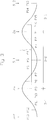
- Fig. 2 which illustrates the amplitudes at the locations P9, P10, P11, P12 and P13 along the Z-axis of Fig. 1B in a resonant state whose resonant frequency is 18. 877 kHz, three or four amplitudes at three or four X-coordinate values and at one Y-coordinate value were measured.
- the amplitude at the location P9 was about 4.4 mm
- the amplitude at the location P10 was about 1.6 mm
- the amplitude at the location P11 was about 0.3 mm
- the amplitude at the location P12 was about 1.5 mm
- the amplitude at the location P13 was about 2.2 mm. Therefore, the amplitude at the location P11 was minimum, while the amplitude at the location P9 was maximum.
- the amplitudes at the locations P10 and P12 were medium.
- the amplitude at the location P13 is smaller than the amplitude at the location P9, because the coupling bar 5-2 is located at the location P13 to suppress the vibration of the portion of the semi-circular piezoelectric actuator 3-2 at the location P13. That is, if no coupling bar is present at the location P13, the amplitude at the location P13 would be considered to be the same as the amplitude at the location P9, i.e., larger than 2.2mm.
- the amplitudes at the locations P1, P2, ⁇ , P16 of the circumferential line L in a resonant state can be as shown in Fig. 3 .
- a drive voltage V Y1 is applied to the entire semi-circular piezoelectric actuator 3-1.
- the amplitudes at the locations P1, P2, P8 and P9 are opposite in phase to those at the locations P4, P5 and P6, a drive voltage V Y2 opposite in phase to the drive voltage V Y1 is applied to the entire semi-circular piezoelectric actuator 3-2.
- the drive power by the drive voltages V Y1 and V Y2 would be decreased.
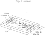
- Fig. 4 is a perspective view illustrating a second prior art one-dimensional optical deflector (see: Figs. 26, 27, 28 and 29 of JP2010-197994A and US2010/0195180A1 ).
- the second prior art one-dimensional optical deflector is constructed by a circular mirror 101, a pair of torsion bars 102a and 102b arranged along a Y-axis each having an end coupled to the circumference of the mirror 101, a pair of linear piezoelectric actuators 103a-1 and 103a-2 each having an end coupled to the torsion bar 102a, a pair of linear piezoelectric actuators 103b-1 and 103b-2 each having an end coupled to the torsion bar 102b, and a rectangular fixed frame 104 coupled to other ends of the linear piezoelectric actuators 103a-1, 103a-2, 103b-1 and 103b-2.
- a drive voltage V Y1 is applied to the piezoelectric portions 103a-11 and 103b-11, while a drive voltage V Y2 opposite in phase to the drive voltage V Y1 is applied to the piezoelectric portions 103a-21 and 103b-21.
- the rocking angle of the mirror 1 can be maximum under the same drive voltages V Y1 and V Y2 .
- Fig. 5 is a perspective view illustrating a third prior art one-dimensional optical deflector (see: Figs. 30, 31, 32, 33 and 34 of JP2010-197994A and US2010/0195180A1 ).
- Fig. 5 further piezoelectric portions 103a-12, 103a-22, 103b-12 and 103b-22 separated from the piezoelectric portions 103a-11, 103a-21, 103b-11 and 103b-21 are formed on the linear piezoelectric actuators 103a-1, 103a-2, 103b-1 and 103b-2, respectively, of Fig. 4 .
- the drive voltage V Y1 is applied to the piezoelectric portions 103a-22 and 103b-22
- the drive voltage V Y2 is applied to the piezoelectric portions 103a-12 and 103b-12.
- the rocking angle of the mirror 1 can be further increased under the same drive voltages V Y1 and V Y2 .
- the length L P of the piezoelectric portions 103a-11, 103a-21, 103b-11 and 103b-22 is determined in accordance with the maximum value of the flexing angle of the linear piezoelectric actuators 103a-1, 103a-2, 103b-1 and 103b-2 when no torsion bar is coupled thereto or the maximum value of the moment of the linear piezoelectric actuators 103a-1, 103a-2, 103b-1 and 103b-2 when the torsion bars 102a and 102b are fixed.
- the presently disclosed subject matter seeks to solve one or more of the above-described problems.
- an optical deflector is provided as set forth in claim 1. Preferred embodiments of the present invention may be gathered from the dependent claims.
- the drive power can be increased and the reliability can be enhanced.
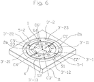
- Fig. 6 which illustrates a first embodiment of the one-dimensional optical deflector according to the presently disclosed subject matter
- the semi-circular piezoelectric actuators 3-1 and 3-2 of Fig. 1 are replaced by semi-circular piezoelectric actuators 3'-1 and 3'-2, respectively.
- radial axes C1', C2', C3', C4', C5' and C6' are defined at 60° intervals centered at a point "0" on a plane of the fixed frame 4.
- an X-axis is defined by a radial line between the radial axes C2' and C3'
- a Y-axis is defined by the radial axis C1'
- a Z-axis is defined to be perpendicular to the X-axis and the Y-axis.
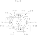
- the semi-circular piezoelectric actuator 3' -1 includes piezoelectric portions 3' -11, 3' -12 and 3' -13 made of PZT separated by slits S1 and S2 arranged on the radial axes C2' and C3' , respectively.
- the semi-circular piezoelectric actuator 3' -2 includes piezoelectric portions 3' -21, 3' -22 and 3' -23 made of PZT separated by slits S3 and S4 arranged on the radial axes C5' and C6', respectively.
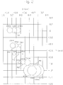
- the positions of the slits S1, S2, S3 and S4 are determined by a polarization polarity distribution on the semi-circular piezoelectric actuators 3' -1 and 3' -2 as illustrated in Fig. 7 obtained by performing a predetermined polarization simulation upon the one-dimensional optical deflector of Fig. 6 where piezoelectric portions with no slits are hypothetically provided in the semi-circular piezoelectric actuators 3' -1 and 3' -2 and a predetermined rocking operation is performed on the mirror 1.
- the polarization polarity of polarization areas as indicated by G1 is opposite to the polarization polarity of polarization areas as indicated by G2.
- one of the polarization polarities represents a compression stress state, while the other represents a tension stress state. That is, the positions of the slits S1, S2, S3 and S4 of Fig. 6 correspond to boundaries between the polarization polarity areas indicated by G1 and the polarization polarity areas indicated by G2 in Fig. 7 . Therefore, as illustrated in Fig.
- a drive voltage V Y1 is applied to the piezoelectric portions 3' -11 and 3' -13 of the semi-circular piezoelectric actuator 3' -1 and the piezoelectric portion 3' -22 of the semi-circular piezoelectric actuator 3' -2, while a drive voltage V Y2 opposite in phase to the drive voltage V Y1 is applied to the piezoelectric portion 3' -12 of the semi-circular piezoelectric actuator 3' -1 and the piezoelectric portions 3' -21 and 3' -23 of the semi-circular piezoelectric actuator 3' -2.
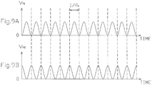
- the drive voltage V Y1 is a sinusoidal-wave voltage whose frequency f R is a resonant frequency as illustrated in Fig. 9A
- the drive voltage V Y2 is a sinusoidal-wave voltage as illustrated in Fig. 9B which is opposite in phase to the sinusoidal-wave drive voltage V Y1 .
- Figs. 9A and 9B note that the sinusoidal-wave voltages V Y1 and V Y2 are monopolar. As a result, the areas indicated by G1 and G2 of the semi-circular piezoelectric actuators 3' -1 and 3' -2 are moved in the same phase with respect to the Y-axis, to thereby effectively rock the mirror 1 with respect to the Y-axis.
- the amplitudes of the drive voltages V Y1 and V Y2 were required to be 10V in the one-dimensional optical deflector of Fig. 6
- the amplitudes of the drive voltages V Y1 and V Y2 were required to be 20V or more in the one-dimensional optical deflector of Fig. 1 .
- the rocking angle of the mirror 1 by the same amplitudes of the drive voltages V Y1 and V Y2 can be larger in the one-dimensional optical deflector of Fig. 6 than in the one-dimensional optical deflector of Fig.
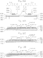
- Figs. 10A, 10B, 10C, and 10D are cross-sectional views of the optical deflector of Fig. 6 .
- Fig. 10A is a cross-sectional view of the entire optical deflector of Fig. 6
- Figs. 10B, 10C and 10D are cross-sectional views of the semi-circular piezoelectric actuator 3' -1 (3' -2) of Fig. 6 .
- a monocrystalline silicon support layer 1001, an intermediate silicon dioxide layer 1002 and a monocrystalline silicon active layer 1003 are formed by a silicon-on-insulator (SOI) substrate.
- reference numeral 1004 designates a silicon dioxide layer
- 1005 designates a lower electrode layer of a double layer made of Ti, TiO 2 or TiO x (0 ⁇ x ⁇ 2) and Pt
- 1006 designates a PZT layer
- 1007 designates an upper electrode layer made of Pt, Au or the like
- 1008 designates an about 100 to 500 nm thick metal layer made of Al, Ag, Au, Pt or the like.
- the mirror 1 is constructed by the monocrystalline silicon active layer 1003 serving as a vibration plate and the metal layer 1008 serving as a reflector.
- the semi-circular piezoelectric actuators 3' -1 and 3' -2 are constructed by the intermediate silicon layer 1002, the monocrystalline silicon active layer 1003, the silicon dioxide layer 1004, the lower electrode layer 1005, the PZT layer 1006 and the upper electrode layer 1007. Particularly, the lower electrode layer 1005, the PZT layer 1006 and the upper electrode layer 1007 form the piezoelectric portions 3' -11, 3' -12, 3' -13, 3' -21, 3' -22 and 3' -23.
- the fixed frame 4 is constructed by the monocrystalline silicon layer 1001, the intermediate silicon layer 1002, the monocrystalline silicon active layer 1003 and the silicon dioxide layer 1004.
- the semi-circular piezoelectric actuators 3'-1 (3'-2) can entirely include the lower electrode layer 1005 as illustrated in Fig. 10C , or can entirely include the lower electrode layer 1005 and the PZT layer 1006 as illustrated in Fig. 10D .
- portions of the PZT layer 1006 without the upper electrode layer 1007 are inactivated, so that the semi-circular piezoelectric actuators 3' -1 (3' -2) of Fig. 10C or 10D can serve as the semi-circular piezoelectric actuators 3' -1 (3' -2) of Fig. 10B .
- the structure of the one-dimensional optical deflector as illustrated in Fig. 10 can be manufactured by semiconductor manufacturing technology and micro electro mechanical systems (MEMS) technology (see : JP 2009-169326 and JP 2009-223165 ).
- MEMS micro electro mechanical systems
- a method for designing the one-dimensional optical deflector of Fig. 6 is as follows.
- a one-dimensional optical deflector of Fig. 6 without slits S1, S2, S3 and S4 is designed.
- piezoelectric portions are provided at least on the piezoelectric actuators 3'-1 and 3'-2.
- a predetermined polarization simulation is performed upon the designed one-dimensional deflector without slits S1, S2, S3 and S4 to obtain a polarization polarity distribution as illustrated in Fig. 7 while a predetermined rocking operation is performed upon the mirror 1.
- the locations of the slits S1, S2, S3 and S4 are determined in accordance with boundaries between the polarization polarity areas of the polarization polarity distribution.
- the piezoelectric portions 3' -11, 3' -12, 3' -13, 3' -21, 3' -22 and 3' -23 are determined in accordance with the slits S1, S2, S3 and S4.
- a semi-diamond (or semi-lozenge)-shaped piezoelectric actuator 3" -1 including piezoelectric portions 3" -11, 3" -12 and 3" -13 and a semi-diamond-shaped piezoelectric actuator 3"-2 including the piezoelectric portions 3" -21, 3" -22 and 3" -23 and a diamond-shaped fixed frame 4' are provided instead of the semiconductor piezoelectric actuator 3' -1 including the piezoelectric portions 3' -11, 3' -12 and 3' -13 and the semi-circular piezoelectricactuator3' -21, 3' -22 and 3' -23 and the rectangular fixed frame 4, respectively, of Fig. 6 .
- the width of the semi-diamond-shaped piezoelectric actuators 3" -1 and 3" -2 is gradually increased from the coupling portions 5-1 and 5-2 as indicated by A (see: Fig. 12 ) to the torsion bars 2a and 2b as indicated by B (see: Fig. 12 ).
- the rocking angle of the mirror 1 can be increased under the same drive voltage V Y1 and V Y2 .
- the piezoelectric portions 3" -11, 3" -12 and 3' -13 made of PZT are separated by slits S1' and S2' arranged on the radial axes C2' and C3', respectively.
- the piezoelectric portions 3" -21, 3" -22 and 3" -23 made of PZT are separated by slits S3' and S4' arranged on the radial axes C5" and C6", respectively.
- the positions of the slits S1', S2' , S3' and S4' are determined by a polarization polarity distribution on the semi-diamond-shaped piezoelectric actuators 3" -1 and 3" -2 as illustrated in Fig. 12 obtained by performing a predetermined polarization simulation upon the one-dimensional optical deflector of Fig. 11 where piezoelectric portions with no slits are hypothetically provided in the semi-diamond-shaped piezoelectric actuators 3" -1 and 3" -2 and a predetermined rocking operation is performed on the mirror 1.
- a sinusoidal-wave drive voltage V Y1 is applied to the piezoelectric portions 3" -11 and 3" -13 of the semi-diamond-shaped piezoelectric actuator 3" -1 and the piezoelectric portion 3" -22 of the semi-diamond-shaped piezoelectric actuator 3" -2, while a sinusoidal-wave drive voltage V Y2 opposite in phase to the drive voltage V Y1 is applied to the piezoelectric portion 3" -12 of the semi-diamond-shaped piezoelectric actuator 3" -1 and the piezoelectric portions 3" -21 and 3" -23 of the semi-diamond-shaped piezoelectric actuator 3" -2.
- the structure of the one-dimensional optical deflector of Fig. 11 is similar to that of the one-dimensional optical deflector of Fig. 6 as illustrated in Fig. 10 . Also, the method for designing the one-dimensional optical deflector of Fig. 11 is similar to the method for designing the one-dimensional optical deflector of Fig. 6 .
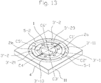
- Fig. 13 which illustrates a third embodiment of the one-dimensional optical deflector according to the presently disclosed subject matter
- the piezoelectric portions 3' -12 and 3' -22 are removed from the semi-circular piezoelectric actuators 3' -1 and 3' -2 of Fig. 6 .
- a sinusoidal-wave drive voltage V Y1 as illustrated in Fig. 9A is applied to the piezoelectric portions 3' -11 and 3' -13 of the semi-circular piezoelectric actuator 3' -1, while a sinusoidal-wave drive voltage V Y2 as illustrated in Fig. 9B opposite in phase to the drive voltage V Y1 is applied to the piezoelectric portions 3' -21 and 3' -23 of the semi-circular piezoelectric actuator 3' -2.
- the amplitudes of the drive voltages V Y1 and V Y2 were required to be 11 to 12V in the one-dimensional optical deflector of Fig. 13 . Therefore, in the same way as in the one-dimensional optical deflector of Fig. 6 , the power consumption can be decreased, and the deterioration of the piezoelectric portions made of PZT can be suppressed to enhance the reliability.
- the structure of the one-dimensional optical deflector of Fig. 13 is similar to that of the one-dimensional optical deflector of Fig. 6 as illustrated in Fig. 10 . Also, the method for designing the one-dimensional optical deflector of Fig. 13 is similar to the method for designing the one-dimensional optical deflector of Fig. 6 .
- the one-dimensional optical deflector of Fig. 6 where no drive voltage is applied to the piezoelectric portions 3' -12 and 3' -22 can be used as the one-dimensional optical deflector of Figs. 13 and 14 .
- no drive voltage is applied to the piezoelectric portion 3' -12 of the semi-circular piezoelectric actuator 3' -1 and the piezoelectric portion 3' -22 of the semi-circular piezoelectric actuator 3' -2.
- Fig. 15 which illustrates a fourth embodiment of the one-dimensional optical deflector according to the presently disclosed subject matter
- torsion bars 2'a and 2'b are provided instead of the torsion bars 2a and 2b, respectively, of Fig. 6 . Since the torsion bars 2'a and 2'b are coupled between the outer circumference of the mirror 1 and the inner circumference of the fixed frame 4 through the semi-circular piezoelectric actuators 3' -1 and 3' -2, the torsion bars 2'a and 2'b can be stably twisted by the piezoelectric actuators 3' -1 and 3' -2. Also, since the mirror 1 is supported by a four-point support at the fixed frame 4, the support of the mirror 1 is more stable in the one-dimensional optical deflector of Fig. 15 than in the one-dimensional optical deflector of Fig. 6 .
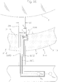
- a piezoelectric sensor 1501 is provided at a portion crossing between the torsion bar 2b and the semi-circular piezoelectric actuator 3'-1.
- the piezoelectric sensor 1501 is constructed by the lower electrode layer 1005, the PZT layer 1006 and the upper electrode layer 1007 in the same way as those of Fig. 10 , in order to sense rocking vibrations of the torsion bar 2b caused by the semi-circular piezoelectric actuator 3'-1.
- the piezoelectric sensor 1501 senses a strong stress due to the rocking vibrations of the torsion bar 2b which would be concentrated at an inner side portion of the semi-circular piezoelectric actuator 3'-1 in the vicinity of the torsion bar 2b.
- the piezoelectric sensor 1501 is arranged at a width portion having a width of less than 0.18 ⁇ W from the inner circumference of the semi-circular piezoelectric actuator 3'-1.
- a sense conductive layer 1601 is connected from the upper electrode layer (not shown) of the piezoelectric sensor 1501 over the torsion bar 2b to a sense pad P S on the fixed frame 4.
- ground conductive layers 1602 and 1603 are arranged to sandwich the sense conductive layer 1601, so that the sense conductive layer 1601 is electrostatically shielded by the ground conductive layers 1602 and 1603, thus preventing the sense conductive layer 1601 from crosstalking with the drive voltages V Y1 and V Y2 at the piezoelectric portion 3'-13 of the semi-circular piezoelectric actuator 3'-1 and the piezoelectric portion 3'-21 of the semi-circular piezoelectric actuator 3'-2.
- the ground conductive layers 1602 and 1603 are connected over the torsion bar 2b to a ground pad P GND on the fixed frame 4.
- a sense voltage V S of the piezoelectric sensor 1501 is supplied from the sense conductive layer 1601 to the sense pad P S , and then is supplied to a control unit (not shown) which controls the drive voltages V Y1 and V Y2 . Therefore, the frequency of the drive voltages V Y1 and V Y2 is controlled by the control unit, so that the sense voltage V S is brought close to its maximum value, thus realizing a resonance state.
- the structure of the one-dimensional optical deflector of Fig. 15 is similar to that of the one-dimensional optical deflector of Fig. 6 as illustrated in Fig. 10 . Also, the method for designing the one-dimensional optical deflector of Fig. 15 is similar to the method for designing the one-dimensional optical deflector of Fig. 6 .
- the one-dimensional optical deflector of Fig. 6 is applied to a light scanning system as illustrated in Fig. 17 .
- a light source 1701 emits a light beam BM and transmits it to the mirror 1 of the one-dimensional optical deflector of Fig. 6 .
- a control unit 1702 controls the light source 1701, so that the control unit 1702 turns ON and OFF the light source 1701, as occasion demands. Also, the control unit 1702 controls the sinusoidal-wave drive voltages V Y1 and V Y2 as illustrated in Figs.
- control unit 1702 turns ON the light source 1701 for a half period of the sinusoidal-wave voltage V Y1 and turns OFF the light source 1701 for the other half period of the sinusoidal-wave voltage V Y1 .
- the light beam BM is reflected by the mirror 1 to emit a scanning light beam SB.
- the control unit 1702 is constructed by a microcomputer including a central processing unit (CPU), a read-only memory (ROM), a random access memory (RAM) and the like.
- the one-dimensional optical deflector of Fig. 11 , 13 or 15 can also be applied to the light scanning system of Fig. 17 .
- the mirror 1 is circular; however, the mirror 1 can be an ellipse.
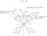
- the slits S1, S2, S3 and S4 are arranged along a 60°, 120°, 240° and 300° -angled direction with respect to the rocking direction of the mirror 1.
- Fig. 1 illustrates that the slits S1, S2, S3 and S4 (S1', S2', S3' and S4') are arranged along a 60°, 120°, 240° and 300° -angled direction with respect to the rocking direction of the mirror 1.
- the slit S1 (S1') can be arranged along a first radial direction which is +30° to +60° -angled with respect to the rocking direction
- the slit S2 (S2') can be arranged along a second radial direction which is +120° to +150° -angled with respect to the rocking direction
- the slit S3 (S3') can be arranged along a third radial direction which is +210° to +240° -angled with respect to the rocking direction
- the slit S4 (S4') can be arranged along a fourth radial direction which is +300° to +330° -angled with respect to the rocking direction.
- the slits S1 and S3 are arranged along a first diameter direction which is obtained by inclining the rocking direction (axis) by a first predetermined angle between +30° and +60°, while the slits S2 and S4 (S2' and S4') are arranged along a second diameter direction which is obtained by inclining the rocking direction (axis) by a second predetermined angle between -30° and -60° .
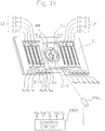
- Fig. 19 which is a perspective view illustrating a two-dimensional optical deflector to which the one-dimensional optical deflector of Fig. 6 is applied
- the rectangular fixed frame 4 of Fig. 6 serves as a movable frame 4M.
- a rectangular fixed frame 11 is provided to surround the movable frame 4M.
- a pair of outer meander-type piezoelectric actuators 12 and 13 between the fixed frame 11 and the movable frame 4M and serving as cantilevers for rocking the mirror 1 around the X-axis.
- the piezoelectric actuators 12 and 13 are arranged opposite to each other with respect to the X-axis.
- the outer piezoelectric actuator 12 is constructed by piezoelectric cantilevers 12-1, 12-2, 12-3 and 12-4 which are serially-coupled from the fixed frame 11 to the movable frame 4M. Also, each of the piezoelectric cantilevers 12-1, 12-2, 12-3 and 12-4 are in parallel with the Y-axis. Therefore, the piezoelectric cantilevers 12-1, 12-2, 12-3 and 12-4 are folded at every cantilever or meandering from the fixed frame 11 to the movable frame 4M, so that the amplitudes of the piezoelectric cantilevers 12-1, 12-2, 12-3 and 12-4 can be changed along directions perpendicular to the X-axis.
- the outer piezoelectric actuator 13 is constructed by piezoelectric cantilevers 13-1, 13-2, 13-3 and 13-4 which are serially-coupled from the fixed frame 11 to the movable frame 4M. Also, each of the piezoelectric cantilevers 13-1, 13-2, 13-3 and 13-4 are in parallel with the Y-axis. Therefore, the piezoelectric cantilevers 13-1, 13-2, 13-3 and 13-4 are folded at every cantilever or meandering from the fixed frame 11 to the movable frame 4M, so that the amplitudes of the piezoelectric cantilevers 13-1, 13-2, 13-3 and 13-4 can be changed along directions perpendicular to the X-axis.
- the number of piezoelectric cantilevers in each of the outer piezoelectric actuators 12 and 13 can be other values such as 2, 6, 8, ⁇ .
- pads P X1 and P X2 are connected to a control unit 1901 which applies a drive voltage V X1 to the pad P X1 , and applies a drive voltage V X2 to the pad P X2 .
- the drive voltages V X1 and V X2 opposite in phase to each other are saw-tooth-shaped, and have a frequency of 15 kHz.
- the pad P X1 is connected via conductive layers (not shown) to the upper electrode layers of the odd-numbered piezoelectric cantilevers 12-1, 12-3, 13-1 and 13-3 of the outer piezoelectric actuators 12 and 13.
- the pad P X2 is connected via conductive layers to the upper electrode layers of the even-numbered piezoelectric cantilevers 12-2, 12-4, 13-2 and 13-4 of the outer piezoelectric actuators 12 and 13.
- pads P Y1 , P Y2 , P S and P GND are provided on the frame 11 .
- the pad P Y1 is connected via conductive layers (not shown) to the upper electrode layer of the semi-circular piezoelectric actuator 3' -1.
- the pad P Y2 is connected via conductive layers (not shown) to the upper electrode layer of the semi-circular piezoelectric actuator 3' -2.
- the pad P S is connected via conductive layers (not shown) to the upper electrode layer of the piezoelectric sensor (not shown).
- the pad P GND is connected via conductive layers (not shown) to the lower electrode layers of all the piezoelectric actuators and the piezoelectric sensor.
- a light source 1901 corresponding to the light source 1701 of Fig. 17 and a control unit 1902 corresponding to the control unit 1702 of Fig. 17 are provided.
- the control unit 1902 further controls the drive voltages V Y1 and V Y2 in accordance with the sense voltage V S and also, controls the drive voltages V X1 and V X2 .
- the one-dimensional optical deflector of Fig. 11 , 13 or 15 can also be applied to the two-dimensional optical deflector of Fig. 19 .
- the piezoelectric actuators are semi-circular or semi-diamond-shaped; however, the piezoelectric actuators can be of another bent-type.
Landscapes
- Physics & Mathematics (AREA)
- General Physics & Mathematics (AREA)
- Optics & Photonics (AREA)
- Mechanical Light Control Or Optical Switches (AREA)
- Mechanical Optical Scanning Systems (AREA)
- Micromachines (AREA)
Claims (6)
- Déflecteur optique comprenant :un miroir (1) ;un cadre (4, 4') entourant ledit miroir (1) ;des première et deuxième barres de torsion (2a, 2b, 2'a, 2'b) disposées de façon opposée le long d'un premier axe dudit cadre (4, 4'), chacune desdites première et deuxième barres de torsion (2a, 2b, 2'a, 2'b) ayant une extrémité couplée à une circonférence dudit miroir (1) ;des premier et deuxième actionneurs piézoélectriques semi-circulaires (3'-1, 3'-2, 3"-1, 3"-2) opposés l'un à l'autre par rapport audit miroir (1), pour faire basculer ledit miroir (1) autour dudit premier axe, chacun desdits premier et deuxième actionneurs piézoélectriques semi-circulaires (3'-1, 3'-2, 3"-1, 3"-2) étant couplé à la fois auxdites première et deuxième barres de torsion (2a, 2b, 2'a, 2'b) ; etdes première et deuxième barres de couplage (5-1, 5-2) couplées chacune entre ledit cadre (4, 4') et un desdits premier et deuxième actionneurs piézoélectriques semi-circulaires (3'-1, 3'-2, 3"-1, 3"-2) et agencées le long d'un deuxième axe perpendiculaire audit premier axe ; etune unité de commande (1702) adapté pour commander lesdits premier et deuxième actionneurs piézoélectriques semi-circulaires (3'-1, 3'-2, 3"-1, 3"-2),chacun desdits premier et deuxième actionneurs piézoélectriques semi-circulaires (3'-1, 3'-2, 3"-1, 3"-2) étant divisé en première, deuxième et troisième zones (G1, G2) depuis ladite première barre de torsion (2a, 2'a) jusqu'à ladite deuxième barre de torsion (2b, 2'b) conformément à des limites agencées le long d'une première direction radiale selon une direction faisant un angle de +30° à +60°, d'une deuxième direction radiale selon une direction faisant un angle de +120° à +150°, d'une troisième direction radiale selon une direction faisant un angle de +210° à +240°, et d'une quatrième direction radiale selon une direction faisant un angle de +300° à +330° par rapport audit premier axe,la deuxième zone (G2) dudit premier actionneur piézoélectrique semi-circulaire (3'-1, 3"-1) étant entre lesdites première et deuxième directions radiales,la deuxième zone (G2) dudit deuxième actionneur piézoélectrique semi-circulaire (3'-2, 3"-2) étant entre lesdites troisième et quatrième directions radiales,des premières parties piézoélectriques (3'-11, 3'-13, 3'-22, 3"-11, 3"-13, 3"-22) étant formées dans les première et troisième zones dudit premier actionneur piézoélectrique semi-circulaire (3'-1, 3"-1) et la deuxième zone dudit deuxième actionneur piézoélectrique semi-circulaire (3'-2, 3"-2),des deuxièmes parties piézoélectriques (3'-21, 3'-23, 3'-12, 3"-21, 3"-23, 3"-12) étant formées dans les première et troisième zones dudit deuxième actionneur piézoélectrique semi-circulaire (3'-2, 3"-2) et la deuxième zone dudit premier actionneur piézoélectrique semi-circulaire (3'-1, 3"-1),ladite unité de commande (1702) étant adaptée pour appliquer une première tension de commande (VY1) auxdites premières parties piézoélectriques (3'-11, 3'-13, 3'-22, 3"-11, 3"-13, 3"-22) et une deuxième tension de commande (VY2) opposée en phase à ladite première tension de commande (VY1) auxdites deuxièmes parties piézoélectriques (3'-21, 3'-23, 3'-12, 3"-21, 3"-23, 3"-12).
- Déflecteur optique selon la revendication 1, dans lequel lesdits premier et deuxième actionneurs piézoélectriques semi-circulaires (3"-1, 3"-2) sont en forme de demi-losange, et ledit cadre (4') est en forme de losange.
- Déflecteur optique selon la revendication 2, dans lequel une largeur desdits premier et deuxième actionneurs piézoélectriques semi-circulaires (3"-1, 3"-2) est progressivement accrue à partir desdites première et deuxième barres de couplage (5-1, 5-2) jusqu'auxdites première et deuxième barres de torsion (2'a, 2'b).
- Déflecteur optique selon la revendication 1, dans lequel lesdites première et deuxième barres de torsion (2'a, 2'b) sont couplées au moyen desdits premier et deuxième actionneurs piézoélectriques semi-circulaires (3'-1, 3'-2) à une circonférence intérieure dudit cadre (4).
- Déflecteur optique selon la revendication 4, comprenant en outre :un capteur piézoélectrique (1501) au niveau d'une partie se croisant entre une desdites première et deuxième barres de torsion (2a, 2b) et un desdits premier et deuxième capteurs piézoélectriques semi-circulaires (3'-1, 3'-2) ; etune couche conductrice de lecture (1601) connectée depuis ledit un desdits premier et deuxième actionneurs piézoélectriques semi-circulaires (3'-1, 3'-2) sur ladite une desdites première et deuxième barres de torsion (2a, 2b) jusqu'à un plot de détection (PS) sur ledit cadre (4) ; etdes première et deuxième couches conductrices de masse (1602, 1603) prenant en sandwich ladite couche conductrice de lecture (1601) et connectées sur ladite une desdites première et deuxième barres de torsion (2a, 2b) à un plot de masse (PGND) sur ledit cadre (4).
- Déflecteur optique selon la revendication 1, comprenant en outre :un autre cadre (11) entourant ledit cadre (4M) ; etdes premier et deuxième actionneurs piézoélectriques extérieurs (12, 13), couplés entre ledit cadre (4M) et ledit autre cadre (11), pour faire basculer ledit miroir (1) autour d'un deuxième axe perpendiculaire audit premier axe.
Applications Claiming Priority (1)
| Application Number | Priority Date | Filing Date | Title |
|---|---|---|---|
| JP2013112342A JP6092713B2 (ja) | 2013-05-28 | 2013-05-28 | 光偏向器 |
Publications (2)
| Publication Number | Publication Date |
|---|---|
| EP2808719A1 EP2808719A1 (fr) | 2014-12-03 |
| EP2808719B1 true EP2808719B1 (fr) | 2021-08-25 |
Family
ID=50972441
Family Applications (1)
| Application Number | Title | Priority Date | Filing Date |
|---|---|---|---|
| EP14170118.5A Active EP2808719B1 (fr) | 2013-05-28 | 2014-05-27 | Déflecteur optique comprenant des parties piézoélectriques séparées sur des actionneurs piézoélectriques |
Country Status (3)
| Country | Link |
|---|---|
| US (1) | US9395536B2 (fr) |
| EP (1) | EP2808719B1 (fr) |
| JP (1) | JP6092713B2 (fr) |
Families Citing this family (19)
| Publication number | Priority date | Publication date | Assignee | Title |
|---|---|---|---|---|
| JP5916668B2 (ja) * | 2013-07-17 | 2016-05-11 | 富士フイルム株式会社 | ミラー駆動装置及びその駆動方法 |
| JP5916667B2 (ja) | 2013-07-17 | 2016-05-11 | 富士フイルム株式会社 | ミラー駆動装置及びその駆動方法 |
| WO2016052548A1 (fr) * | 2014-09-30 | 2016-04-07 | 富士フイルム株式会社 | Dispositif d'entraînement de miroir et procédé d'entraînement pour celui-ci |
| EP3203298B1 (fr) * | 2014-09-30 | 2021-07-14 | FUJIFILM Corporation | Dispositif d'entraînement de miroir et son procédé d'entraînement |
| JP6560897B2 (ja) | 2015-05-20 | 2019-08-14 | スタンレー電気株式会社 | 圧電膜の積層体とその製造方法及び光スキャナ |
| JP6741933B2 (ja) | 2015-10-02 | 2020-08-19 | ミツミ電機株式会社 | 光走査モジュール、光走査制御装置 |
| JP6023379B2 (ja) * | 2016-04-26 | 2016-11-09 | ヤフー株式会社 | 評価装置、評価方法及び評価プログラム |
| IT201600079604A1 (it) * | 2016-07-28 | 2018-01-28 | St Microelectronics Srl | Struttura oscillante con attuazione piezoelettrica, sistema e metodo di fabbricazione |
| IT201600131849A1 (it) * | 2016-12-28 | 2018-06-28 | St Microelectronics Srl | Dispositivo mems con azionamento piezoelettrico, sistema mems proiettivo includente il dispositivo mems e relativo metodo di comando |
| WO2019167615A1 (fr) * | 2018-02-27 | 2019-09-06 | パイオニア株式会社 | Déflecteur optique |
| DE102018215528A1 (de) | 2018-09-12 | 2020-03-12 | Robert Bosch Gmbh | Mikromechanisches Bauteil und Herstellungsverfahren für ein mikromechanisches Bauteil |
| DE102018220422A1 (de) * | 2018-11-28 | 2020-05-28 | Robert Bosch Gmbh | Aktuationseinrichtung für ein mikromechanisches Bauelement, mikromechanisches Bauelement und Verfahren zum Herstellen eines mikromechanisches Bauelements |
| CN113574007B (zh) * | 2019-03-28 | 2024-12-03 | 富士胶片株式会社 | 微镜器件及微镜器件的驱动方法 |
| EP3961289A4 (fr) * | 2019-04-26 | 2022-06-15 | FUJIFILM Corporation | Dispositif de micro-miroir |
| JP7420645B2 (ja) | 2020-05-25 | 2024-01-23 | スタンレー電気株式会社 | 光走査装置 |
| CN116547229B (zh) * | 2020-11-12 | 2025-10-17 | 华为技术有限公司 | 用于扫描仪技术领域的带振镜的偏转设备 |
| JP7543872B2 (ja) * | 2020-11-20 | 2024-09-03 | セイコーエプソン株式会社 | 光学デバイスの駆動方法、光学システム、及び、表示装置 |
| JP7751997B2 (ja) * | 2021-07-13 | 2025-10-09 | スタンレー電気株式会社 | Mems光偏向器及び光走査装置 |
| US20230290663A1 (en) * | 2022-03-11 | 2023-09-14 | X-Celeprint Limited | Printing components suspended by frames |
Citations (1)
| Publication number | Priority date | Publication date | Assignee | Title |
|---|---|---|---|---|
| EP2827182A1 (fr) * | 2013-07-17 | 2015-01-21 | Fujifilm Corporation | Dispositif d'entraînement de miroir et son procédé de commande |
Family Cites Families (14)
| Publication number | Priority date | Publication date | Assignee | Title |
|---|---|---|---|---|
| JP4146127B2 (ja) * | 2002-01-16 | 2008-09-03 | セイコーインスツル株式会社 | 圧電アクチュエータ及びそれを備えた電子機器 |
| US8780053B2 (en) * | 2007-03-21 | 2014-07-15 | Northwestern University | Vibrating substrate for haptic interface |
| JP4984117B2 (ja) | 2006-07-13 | 2012-07-25 | スタンレー電気株式会社 | 2次元光スキャナ、それを用いた光学装置および2次元光スキャナの製造方法 |
| US8553306B2 (en) | 2007-03-15 | 2013-10-08 | Ricoh Company, Ltd. | Optical deflector and optical device |
| WO2009087883A1 (fr) | 2008-01-10 | 2009-07-16 | Konica Minolta Opto, Inc. | Micro-scanner et procede de commande associe |
| JP5172364B2 (ja) | 2008-01-16 | 2013-03-27 | スタンレー電気株式会社 | 光偏向器 |
| JP5105527B2 (ja) | 2008-01-21 | 2012-12-26 | スタンレー電気株式会社 | 光偏向器 |
| JP5414187B2 (ja) | 2008-03-18 | 2014-02-12 | スタンレー電気株式会社 | 光偏向器 |
| JP5505306B2 (ja) * | 2008-08-22 | 2014-05-28 | コニカミノルタ株式会社 | 駆動装置 |
| JP5493735B2 (ja) * | 2009-01-30 | 2014-05-14 | 株式会社リコー | 偏向ミラー、光走査装置、画像形成装置、および画像投影装置 |
| US9771042B2 (en) * | 2009-06-19 | 2017-09-26 | Tk Holdings Inc. | Occupant classification system |
| JP2011013621A (ja) * | 2009-07-06 | 2011-01-20 | Ricoh Co Ltd | 光偏向器、画像形成装置及び画像投影装置 |
| WO2012176492A1 (fr) | 2011-06-21 | 2012-12-27 | コニカミノルタアドバンストレイヤー株式会社 | Actionneur d'entraînement par résonance, micro-dispositif de balayage et appareil optique |
| JP5857602B2 (ja) | 2011-10-03 | 2016-02-10 | ミツミ電機株式会社 | 光走査装置 |
-
2013
- 2013-05-28 JP JP2013112342A patent/JP6092713B2/ja active Active
-
2014
- 2014-05-20 US US14/282,906 patent/US9395536B2/en active Active
- 2014-05-27 EP EP14170118.5A patent/EP2808719B1/fr active Active
Patent Citations (1)
| Publication number | Priority date | Publication date | Assignee | Title |
|---|---|---|---|---|
| EP2827182A1 (fr) * | 2013-07-17 | 2015-01-21 | Fujifilm Corporation | Dispositif d'entraînement de miroir et son procédé de commande |
Also Published As
| Publication number | Publication date |
|---|---|
| JP6092713B2 (ja) | 2017-03-08 |
| JP2014232180A (ja) | 2014-12-11 |
| EP2808719A1 (fr) | 2014-12-03 |
| US9395536B2 (en) | 2016-07-19 |
| US20140355088A1 (en) | 2014-12-04 |
Similar Documents
| Publication | Publication Date | Title |
|---|---|---|
| EP2808719B1 (fr) | Déflecteur optique comprenant des parties piézoélectriques séparées sur des actionneurs piézoélectriques | |
| US8730549B2 (en) | Two-dimensional optical deflector including piezoelectric sensor on movable frame | |
| US9696541B2 (en) | Two-dimensional optical deflector including two SOI structures and its manufacturing method | |
| EP2503375B1 (fr) | Dispositif d'entraînement pour déflecteur optique utilisant deux tensions à commande en dents de scie asynchrones et son procédé de réglage | |
| EP2645148B1 (fr) | Déflecteur optique | |
| US9488828B2 (en) | Optical deflector apparatus capable of increasing offset deflecting amount of mirror | |
| US9151947B2 (en) | Optical deflector including piezoelectric sensor incorporated into outermost piezoelectric cantilever | |
| US9097897B2 (en) | Optical deflector including narrow piezoelectric sensor element between torsion bar and piezoelectric actuator | |
| EP2781948B1 (fr) | Déflecteur optique comprenant des actionneurs piézoélectriques de type méandre couplés par croisement de barres entre elles | |
| US8482832B2 (en) | Vibrating mirror element | |
| CN104570335B (zh) | 光扫描仪、图像显示装置、头戴式显示器以及平视显示器 | |
| US8817351B2 (en) | Optical deflector including piezoelectric sensor on fixed frame | |
| EP2953125A1 (fr) | Pilote pour déflecteur optique à l'aide de tension d'entraînement en dents de scie combiné et son procédé de commande | |
| US8649080B2 (en) | Two-dimensional optical deflector including only one pair of meander-type piezoelectric actuators and its driver | |
| US9436000B2 (en) | Optical deflector including meander-type piezoelectric actuators and ill-balanced mirror structure | |
| US20150062677A1 (en) | Micromechanical component and method for producing a micromechanical component | |
| JP2011069954A (ja) | 光スキャナ | |
| US9097894B2 (en) | Optical deflector including four coupling bars between support body and frame | |
| JP5554895B2 (ja) | 揺動構造体、及び揺動構造体を用いた揺動体装置 | |
| JP2009210955A (ja) | 光スキャナ | |
| JP2008111882A (ja) | アクチュエータ、光スキャナおよび画像形成装置 | |
| JP2020154229A (ja) | 光学装置 | |
| JP5664711B2 (ja) | アクチュエータ、光スキャナ、および画像形成装置 | |
| JP2019139046A (ja) | 2次元光偏向器 | |
| JP2018025744A (ja) | 圧電アクチュエータ、光偏向器、光走査装置、画像投影装置および移動体 |
Legal Events
| Date | Code | Title | Description |
|---|---|---|---|
| PUAI | Public reference made under article 153(3) epc to a published international application that has entered the european phase |
Free format text: ORIGINAL CODE: 0009012 |
|
| 17P | Request for examination filed |
Effective date: 20140527 |
|
| AK | Designated contracting states |
Kind code of ref document: A1 Designated state(s): AL AT BE BG CH CY CZ DE DK EE ES FI FR GB GR HR HU IE IS IT LI LT LU LV MC MK MT NL NO PL PT RO RS SE SI SK SM TR |
|
| AX | Request for extension of the european patent |
Extension state: BA ME |
|
| R17P | Request for examination filed (corrected) |
Effective date: 20150603 |
|
| RBV | Designated contracting states (corrected) |
Designated state(s): AL AT BE BG CH CY CZ DE DK EE ES FI FR GB GR HR HU IE IS IT LI LT LU LV MC MK MT NL NO PL PT RO RS SE SI SK SM TR |
|
| STAA | Information on the status of an ep patent application or granted ep patent |
Free format text: STATUS: EXAMINATION IS IN PROGRESS |
|
| 17Q | First examination report despatched |
Effective date: 20181130 |
|
| GRAP | Despatch of communication of intention to grant a patent |
Free format text: ORIGINAL CODE: EPIDOSNIGR1 |
|
| STAA | Information on the status of an ep patent application or granted ep patent |
Free format text: STATUS: GRANT OF PATENT IS INTENDED |
|
| INTG | Intention to grant announced |
Effective date: 20210323 |
|
| RAP3 | Party data changed (applicant data changed or rights of an application transferred) |
Owner name: STANLEY ELECTRIC CO., LTD. |
|
| GRAS | Grant fee paid |
Free format text: ORIGINAL CODE: EPIDOSNIGR3 |
|
| GRAA | (expected) grant |
Free format text: ORIGINAL CODE: 0009210 |
|
| STAA | Information on the status of an ep patent application or granted ep patent |
Free format text: STATUS: THE PATENT HAS BEEN GRANTED |
|
| AK | Designated contracting states |
Kind code of ref document: B1 Designated state(s): AL AT BE BG CH CY CZ DE DK EE ES FI FR GB GR HR HU IE IS IT LI LT LU LV MC MK MT NL NO PL PT RO RS SE SI SK SM TR |
|
| REG | Reference to a national code |
Ref country code: GB Ref legal event code: FG4D |
|
| REG | Reference to a national code |
Ref country code: CH Ref legal event code: EP |
|
| REG | Reference to a national code |
Ref country code: IE Ref legal event code: FG4D Ref country code: AT Ref legal event code: REF Ref document number: 1424396 Country of ref document: AT Kind code of ref document: T Effective date: 20210915 |
|
| REG | Reference to a national code |
Ref country code: DE Ref legal event code: R096 Ref document number: 602014079631 Country of ref document: DE |
|
| REG | Reference to a national code |
Ref country code: LT Ref legal event code: MG9D |
|
| REG | Reference to a national code |
Ref country code: NL Ref legal event code: MP Effective date: 20210825 |
|
| REG | Reference to a national code |
Ref country code: AT Ref legal event code: MK05 Ref document number: 1424396 Country of ref document: AT Kind code of ref document: T Effective date: 20210825 |
|
| PG25 | Lapsed in a contracting state [announced via postgrant information from national office to epo] |
Ref country code: RS Free format text: LAPSE BECAUSE OF FAILURE TO SUBMIT A TRANSLATION OF THE DESCRIPTION OR TO PAY THE FEE WITHIN THE PRESCRIBED TIME-LIMIT Effective date: 20210825 Ref country code: SE Free format text: LAPSE BECAUSE OF FAILURE TO SUBMIT A TRANSLATION OF THE DESCRIPTION OR TO PAY THE FEE WITHIN THE PRESCRIBED TIME-LIMIT Effective date: 20210825 Ref country code: HR Free format text: LAPSE BECAUSE OF FAILURE TO SUBMIT A TRANSLATION OF THE DESCRIPTION OR TO PAY THE FEE WITHIN THE PRESCRIBED TIME-LIMIT Effective date: 20210825 Ref country code: NO Free format text: LAPSE BECAUSE OF FAILURE TO SUBMIT A TRANSLATION OF THE DESCRIPTION OR TO PAY THE FEE WITHIN THE PRESCRIBED TIME-LIMIT Effective date: 20211125 Ref country code: PT Free format text: LAPSE BECAUSE OF FAILURE TO SUBMIT A TRANSLATION OF THE DESCRIPTION OR TO PAY THE FEE WITHIN THE PRESCRIBED TIME-LIMIT Effective date: 20211227 Ref country code: ES Free format text: LAPSE BECAUSE OF FAILURE TO SUBMIT A TRANSLATION OF THE DESCRIPTION OR TO PAY THE FEE WITHIN THE PRESCRIBED TIME-LIMIT Effective date: 20210825 Ref country code: FI Free format text: LAPSE BECAUSE OF FAILURE TO SUBMIT A TRANSLATION OF THE DESCRIPTION OR TO PAY THE FEE WITHIN THE PRESCRIBED TIME-LIMIT Effective date: 20210825 Ref country code: BG Free format text: LAPSE BECAUSE OF FAILURE TO SUBMIT A TRANSLATION OF THE DESCRIPTION OR TO PAY THE FEE WITHIN THE PRESCRIBED TIME-LIMIT Effective date: 20211125 Ref country code: AT Free format text: LAPSE BECAUSE OF FAILURE TO SUBMIT A TRANSLATION OF THE DESCRIPTION OR TO PAY THE FEE WITHIN THE PRESCRIBED TIME-LIMIT Effective date: 20210825 Ref country code: LT Free format text: LAPSE BECAUSE OF FAILURE TO SUBMIT A TRANSLATION OF THE DESCRIPTION OR TO PAY THE FEE WITHIN THE PRESCRIBED TIME-LIMIT Effective date: 20210825 |
|
| PG25 | Lapsed in a contracting state [announced via postgrant information from national office to epo] |
Ref country code: PL Free format text: LAPSE BECAUSE OF FAILURE TO SUBMIT A TRANSLATION OF THE DESCRIPTION OR TO PAY THE FEE WITHIN THE PRESCRIBED TIME-LIMIT Effective date: 20210825 Ref country code: LV Free format text: LAPSE BECAUSE OF FAILURE TO SUBMIT A TRANSLATION OF THE DESCRIPTION OR TO PAY THE FEE WITHIN THE PRESCRIBED TIME-LIMIT Effective date: 20210825 Ref country code: GR Free format text: LAPSE BECAUSE OF FAILURE TO SUBMIT A TRANSLATION OF THE DESCRIPTION OR TO PAY THE FEE WITHIN THE PRESCRIBED TIME-LIMIT Effective date: 20211126 |
|
| PG25 | Lapsed in a contracting state [announced via postgrant information from national office to epo] |
Ref country code: NL Free format text: LAPSE BECAUSE OF FAILURE TO SUBMIT A TRANSLATION OF THE DESCRIPTION OR TO PAY THE FEE WITHIN THE PRESCRIBED TIME-LIMIT Effective date: 20210825 |
|
| PG25 | Lapsed in a contracting state [announced via postgrant information from national office to epo] |
Ref country code: DK Free format text: LAPSE BECAUSE OF FAILURE TO SUBMIT A TRANSLATION OF THE DESCRIPTION OR TO PAY THE FEE WITHIN THE PRESCRIBED TIME-LIMIT Effective date: 20210825 |
|
| REG | Reference to a national code |
Ref country code: DE Ref legal event code: R097 Ref document number: 602014079631 Country of ref document: DE |
|
| PG25 | Lapsed in a contracting state [announced via postgrant information from national office to epo] |
Ref country code: SM Free format text: LAPSE BECAUSE OF FAILURE TO SUBMIT A TRANSLATION OF THE DESCRIPTION OR TO PAY THE FEE WITHIN THE PRESCRIBED TIME-LIMIT Effective date: 20210825 Ref country code: SK Free format text: LAPSE BECAUSE OF FAILURE TO SUBMIT A TRANSLATION OF THE DESCRIPTION OR TO PAY THE FEE WITHIN THE PRESCRIBED TIME-LIMIT Effective date: 20210825 Ref country code: RO Free format text: LAPSE BECAUSE OF FAILURE TO SUBMIT A TRANSLATION OF THE DESCRIPTION OR TO PAY THE FEE WITHIN THE PRESCRIBED TIME-LIMIT Effective date: 20210825 Ref country code: EE Free format text: LAPSE BECAUSE OF FAILURE TO SUBMIT A TRANSLATION OF THE DESCRIPTION OR TO PAY THE FEE WITHIN THE PRESCRIBED TIME-LIMIT Effective date: 20210825 Ref country code: CZ Free format text: LAPSE BECAUSE OF FAILURE TO SUBMIT A TRANSLATION OF THE DESCRIPTION OR TO PAY THE FEE WITHIN THE PRESCRIBED TIME-LIMIT Effective date: 20210825 Ref country code: AL Free format text: LAPSE BECAUSE OF FAILURE TO SUBMIT A TRANSLATION OF THE DESCRIPTION OR TO PAY THE FEE WITHIN THE PRESCRIBED TIME-LIMIT Effective date: 20210825 |
|
| PLBE | No opposition filed within time limit |
Free format text: ORIGINAL CODE: 0009261 |
|
| STAA | Information on the status of an ep patent application or granted ep patent |
Free format text: STATUS: NO OPPOSITION FILED WITHIN TIME LIMIT |
|
| PG25 | Lapsed in a contracting state [announced via postgrant information from national office to epo] |
Ref country code: IT Free format text: LAPSE BECAUSE OF FAILURE TO SUBMIT A TRANSLATION OF THE DESCRIPTION OR TO PAY THE FEE WITHIN THE PRESCRIBED TIME-LIMIT Effective date: 20210825 |
|
| 26N | No opposition filed |
Effective date: 20220527 |
|
| PG25 | Lapsed in a contracting state [announced via postgrant information from national office to epo] |
Ref country code: SI Free format text: LAPSE BECAUSE OF FAILURE TO SUBMIT A TRANSLATION OF THE DESCRIPTION OR TO PAY THE FEE WITHIN THE PRESCRIBED TIME-LIMIT Effective date: 20210825 |
|
| REG | Reference to a national code |
Ref country code: CH Ref legal event code: PL |
|
| REG | Reference to a national code |
Ref country code: BE Ref legal event code: MM Effective date: 20220531 |
|
| PG25 | Lapsed in a contracting state [announced via postgrant information from national office to epo] |
Ref country code: MC Free format text: LAPSE BECAUSE OF FAILURE TO SUBMIT A TRANSLATION OF THE DESCRIPTION OR TO PAY THE FEE WITHIN THE PRESCRIBED TIME-LIMIT Effective date: 20210825 Ref country code: LU Free format text: LAPSE BECAUSE OF NON-PAYMENT OF DUE FEES Effective date: 20220527 Ref country code: LI Free format text: LAPSE BECAUSE OF NON-PAYMENT OF DUE FEES Effective date: 20220531 Ref country code: CH Free format text: LAPSE BECAUSE OF NON-PAYMENT OF DUE FEES Effective date: 20220531 |
|
| REG | Reference to a national code |
Ref country code: FR Ref legal event code: PLFP Year of fee payment: 10 |
|
| PG25 | Lapsed in a contracting state [announced via postgrant information from national office to epo] |
Ref country code: IE Free format text: LAPSE BECAUSE OF NON-PAYMENT OF DUE FEES Effective date: 20220527 |
|
| PG25 | Lapsed in a contracting state [announced via postgrant information from national office to epo] |
Ref country code: BE Free format text: LAPSE BECAUSE OF NON-PAYMENT OF DUE FEES Effective date: 20220531 |
|
| PG25 | Lapsed in a contracting state [announced via postgrant information from national office to epo] |
Ref country code: HU Free format text: LAPSE BECAUSE OF FAILURE TO SUBMIT A TRANSLATION OF THE DESCRIPTION OR TO PAY THE FEE WITHIN THE PRESCRIBED TIME-LIMIT; INVALID AB INITIO Effective date: 20140527 |
|
| PG25 | Lapsed in a contracting state [announced via postgrant information from national office to epo] |
Ref country code: MK Free format text: LAPSE BECAUSE OF FAILURE TO SUBMIT A TRANSLATION OF THE DESCRIPTION OR TO PAY THE FEE WITHIN THE PRESCRIBED TIME-LIMIT Effective date: 20210825 Ref country code: CY Free format text: LAPSE BECAUSE OF FAILURE TO SUBMIT A TRANSLATION OF THE DESCRIPTION OR TO PAY THE FEE WITHIN THE PRESCRIBED TIME-LIMIT Effective date: 20210825 |
|
| PG25 | Lapsed in a contracting state [announced via postgrant information from national office to epo] |
Ref country code: MT Free format text: LAPSE BECAUSE OF FAILURE TO SUBMIT A TRANSLATION OF THE DESCRIPTION OR TO PAY THE FEE WITHIN THE PRESCRIBED TIME-LIMIT Effective date: 20210825 |
|
| PGFP | Annual fee paid to national office [announced via postgrant information from national office to epo] |
Ref country code: DE Payment date: 20250402 Year of fee payment: 12 |
|
| PGFP | Annual fee paid to national office [announced via postgrant information from national office to epo] |
Ref country code: GB Payment date: 20250401 Year of fee payment: 12 |
|
| PGFP | Annual fee paid to national office [announced via postgrant information from national office to epo] |
Ref country code: FR Payment date: 20250401 Year of fee payment: 12 |
|
| PG25 | Lapsed in a contracting state [announced via postgrant information from national office to epo] |
Ref country code: TR Free format text: LAPSE BECAUSE OF FAILURE TO SUBMIT A TRANSLATION OF THE DESCRIPTION OR TO PAY THE FEE WITHIN THE PRESCRIBED TIME-LIMIT Effective date: 20210825 |