EP2811529A1 - Halbleiterbauelement aus siliciumcarbid - Google Patents
Halbleiterbauelement aus siliciumcarbid Download PDFInfo
- Publication number
- EP2811529A1 EP2811529A1 EP12867527.9A EP12867527A EP2811529A1 EP 2811529 A1 EP2811529 A1 EP 2811529A1 EP 12867527 A EP12867527 A EP 12867527A EP 2811529 A1 EP2811529 A1 EP 2811529A1
- Authority
- EP
- European Patent Office
- Prior art keywords
- plane
- silicon carbide
- semiconductor device
- carbide semiconductor
- region
- Prior art date
- Legal status (The legal status is an assumption and is not a legal conclusion. Google has not performed a legal analysis and makes no representation as to the accuracy of the status listed.)
- Granted
Links
Images





Classifications
-
- H—ELECTRICITY
- H10—SEMICONDUCTOR DEVICES; ELECTRIC SOLID-STATE DEVICES NOT OTHERWISE PROVIDED FOR
- H10D—INORGANIC ELECTRIC SEMICONDUCTOR DEVICES
- H10D12/00—Bipolar devices controlled by the field effect, e.g. insulated-gate bipolar transistors [IGBT]
- H10D12/01—Manufacture or treatment
- H10D12/031—Manufacture or treatment of IGBTs
-
- H—ELECTRICITY
- H10—SEMICONDUCTOR DEVICES; ELECTRIC SOLID-STATE DEVICES NOT OTHERWISE PROVIDED FOR
- H10D—INORGANIC ELECTRIC SEMICONDUCTOR DEVICES
- H10D30/00—Field-effect transistors [FET]
- H10D30/01—Manufacture or treatment
- H10D30/021—Manufacture or treatment of FETs having insulated gates [IGFET]
- H10D30/028—Manufacture or treatment of FETs having insulated gates [IGFET] of double-diffused metal oxide semiconductor [DMOS] FETs
- H10D30/0291—Manufacture or treatment of FETs having insulated gates [IGFET] of double-diffused metal oxide semiconductor [DMOS] FETs of vertical DMOS [VDMOS] FETs
-
- H—ELECTRICITY
- H10—SEMICONDUCTOR DEVICES; ELECTRIC SOLID-STATE DEVICES NOT OTHERWISE PROVIDED FOR
- H10D—INORGANIC ELECTRIC SEMICONDUCTOR DEVICES
- H10D30/00—Field-effect transistors [FET]
- H10D30/01—Manufacture or treatment
- H10D30/021—Manufacture or treatment of FETs having insulated gates [IGFET]
- H10D30/028—Manufacture or treatment of FETs having insulated gates [IGFET] of double-diffused metal oxide semiconductor [DMOS] FETs
- H10D30/0291—Manufacture or treatment of FETs having insulated gates [IGFET] of double-diffused metal oxide semiconductor [DMOS] FETs of vertical DMOS [VDMOS] FETs
- H10D30/0297—Manufacture or treatment of FETs having insulated gates [IGFET] of double-diffused metal oxide semiconductor [DMOS] FETs of vertical DMOS [VDMOS] FETs using recessing of the gate electrodes, e.g. to form trench gate electrodes
-
- H—ELECTRICITY
- H10—SEMICONDUCTOR DEVICES; ELECTRIC SOLID-STATE DEVICES NOT OTHERWISE PROVIDED FOR
- H10D—INORGANIC ELECTRIC SEMICONDUCTOR DEVICES
- H10D30/00—Field-effect transistors [FET]
- H10D30/60—Insulated-gate field-effect transistors [IGFET]
-
- H—ELECTRICITY
- H10—SEMICONDUCTOR DEVICES; ELECTRIC SOLID-STATE DEVICES NOT OTHERWISE PROVIDED FOR
- H10D—INORGANIC ELECTRIC SEMICONDUCTOR DEVICES
- H10D30/00—Field-effect transistors [FET]
- H10D30/60—Insulated-gate field-effect transistors [IGFET]
- H10D30/64—Double-diffused metal-oxide semiconductor [DMOS] FETs
- H10D30/66—Vertical DMOS [VDMOS] FETs
-
- H—ELECTRICITY
- H10—SEMICONDUCTOR DEVICES; ELECTRIC SOLID-STATE DEVICES NOT OTHERWISE PROVIDED FOR
- H10D—INORGANIC ELECTRIC SEMICONDUCTOR DEVICES
- H10D30/00—Field-effect transistors [FET]
- H10D30/60—Insulated-gate field-effect transistors [IGFET]
- H10D30/64—Double-diffused metal-oxide semiconductor [DMOS] FETs
- H10D30/66—Vertical DMOS [VDMOS] FETs
- H10D30/668—Vertical DMOS [VDMOS] FETs having trench gate electrodes, e.g. UMOS transistors
-
- H—ELECTRICITY
- H10—SEMICONDUCTOR DEVICES; ELECTRIC SOLID-STATE DEVICES NOT OTHERWISE PROVIDED FOR
- H10D—INORGANIC ELECTRIC SEMICONDUCTOR DEVICES
- H10D62/00—Semiconductor bodies, or regions thereof, of devices having potential barriers
- H10D62/40—Crystalline structures
- H10D62/405—Orientations of crystalline planes
-
- H—ELECTRICITY
- H10—SEMICONDUCTOR DEVICES; ELECTRIC SOLID-STATE DEVICES NOT OTHERWISE PROVIDED FOR
- H10D—INORGANIC ELECTRIC SEMICONDUCTOR DEVICES
- H10D62/00—Semiconductor bodies, or regions thereof, of devices having potential barriers
- H10D62/80—Semiconductor bodies, or regions thereof, of devices having potential barriers characterised by the materials
- H10D62/83—Semiconductor bodies, or regions thereof, of devices having potential barriers characterised by the materials being Group IV materials, e.g. B-doped Si or undoped Ge
- H10D62/832—Semiconductor bodies, or regions thereof, of devices having potential barriers characterised by the materials being Group IV materials, e.g. B-doped Si or undoped Ge being Group IV materials comprising two or more elements, e.g. SiGe
- H10D62/8325—Silicon carbide
-
- H—ELECTRICITY
- H10—SEMICONDUCTOR DEVICES; ELECTRIC SOLID-STATE DEVICES NOT OTHERWISE PROVIDED FOR
- H10D—INORGANIC ELECTRIC SEMICONDUCTOR DEVICES
- H10D64/00—Electrodes of devices having potential barriers
- H10D64/01—Manufacture or treatment
- H10D64/013—Manufacture or treatment of electrodes having a conductor capacitively coupled to a semiconductor by an insulator
- H10D64/01366—Manufacture or treatment of electrodes having a conductor capacitively coupled to a semiconductor by an insulator the semiconductor being silicon carbide
-
- H—ELECTRICITY
- H10—SEMICONDUCTOR DEVICES; ELECTRIC SOLID-STATE DEVICES NOT OTHERWISE PROVIDED FOR
- H10D—INORGANIC ELECTRIC SEMICONDUCTOR DEVICES
- H10D64/00—Electrodes of devices having potential barriers
- H10D64/20—Electrodes characterised by their shapes, relative sizes or dispositions
- H10D64/27—Electrodes not carrying the current to be rectified, amplified, oscillated or switched, e.g. gates
- H10D64/311—Gate electrodes for field-effect devices
- H10D64/411—Gate electrodes for field-effect devices for FETs
- H10D64/511—Gate electrodes for field-effect devices for FETs for IGFETs
- H10D64/512—Disposition of the gate electrodes, e.g. buried gates
- H10D64/513—Disposition of the gate electrodes, e.g. buried gates within recesses in the substrate, e.g. trench gates, groove gates or buried gates
-
- H—ELECTRICITY
- H10—SEMICONDUCTOR DEVICES; ELECTRIC SOLID-STATE DEVICES NOT OTHERWISE PROVIDED FOR
- H10P—GENERIC PROCESSES OR APPARATUS FOR THE MANUFACTURE OR TREATMENT OF DEVICES COVERED BY CLASS H10
- H10P50/00—Etching of wafers, substrates or parts of devices
- H10P50/20—Dry etching; Plasma etching; Reactive-ion etching
- H10P50/24—Dry etching; Plasma etching; Reactive-ion etching of semiconductor materials
- H10P50/242—Dry etching; Plasma etching; Reactive-ion etching of semiconductor materials of Group IV materials
-
- H—ELECTRICITY
- H10—SEMICONDUCTOR DEVICES; ELECTRIC SOLID-STATE DEVICES NOT OTHERWISE PROVIDED FOR
- H10D—INORGANIC ELECTRIC SEMICONDUCTOR DEVICES
- H10D62/00—Semiconductor bodies, or regions thereof, of devices having potential barriers
- H10D62/10—Shapes, relative sizes or dispositions of the regions of the semiconductor bodies; Shapes of the semiconductor bodies
- H10D62/124—Shapes, relative sizes or dispositions of the regions of semiconductor bodies or of junctions between the regions
- H10D62/126—Top-view geometrical layouts of the regions or the junctions
- H10D62/127—Top-view geometrical layouts of the regions or the junctions of cellular field-effect devices, e.g. multicellular DMOS transistors or IGBTs
-
- H—ELECTRICITY
- H10—SEMICONDUCTOR DEVICES; ELECTRIC SOLID-STATE DEVICES NOT OTHERWISE PROVIDED FOR
- H10D—INORGANIC ELECTRIC SEMICONDUCTOR DEVICES
- H10D64/00—Electrodes of devices having potential barriers
- H10D64/60—Electrodes characterised by their materials
- H10D64/66—Electrodes having a conductor capacitively coupled to a semiconductor by an insulator, e.g. MIS electrodes
- H10D64/68—Electrodes having a conductor capacitively coupled to a semiconductor by an insulator, e.g. MIS electrodes characterised by the insulator, e.g. by the gate insulator
- H10D64/693—Electrodes having a conductor capacitively coupled to a semiconductor by an insulator, e.g. MIS electrodes characterised by the insulator, e.g. by the gate insulator the insulator comprising nitrogen, e.g. nitrides, oxynitrides or nitrogen-doped materials
-
- H—ELECTRICITY
- H10—SEMICONDUCTOR DEVICES; ELECTRIC SOLID-STATE DEVICES NOT OTHERWISE PROVIDED FOR
- H10P—GENERIC PROCESSES OR APPARATUS FOR THE MANUFACTURE OR TREATMENT OF DEVICES COVERED BY CLASS H10
- H10P50/00—Etching of wafers, substrates or parts of devices
Definitions
- the present invention relates to a silicon carbide semiconductor device, more particularly a silicon carbide semiconductor device including a silicon carbide layer having a surface covered with an insulation film.
- Japanese Patent Laying-Open No. 2002-261275 discloses the following contents.
- a MOS (Metal Oxide Semiconductor) device the plane of 4H type SiC with an oxide film stacked is a ⁇ 03-38 ⁇ plane or a plane having an off angle within 10° relative to the ⁇ 03-38 ⁇ plane. Accordingly, the channel mobility of the MOS device can be increased. This is probably because the density of dangling bonds per unit area of the constituent atom is high due to the SiC ⁇ 0001 ⁇ plane being a hexagonal close-packed plane, such that the interface state is increased to impede mobility of electrons, whereas the ⁇ 03-38 ⁇ plane is deviated from the hexagonal close-packed plane, such that electrons readily move. Furthermore, the reason why particularly high channel mobility is achieved at the ⁇ 03-38 ⁇ plane is probably due to the atomic bondings appearing at the surface relatively periodically despite being different from the close-packed plane.
- the present invention is directed to solving the aforementioned problem.
- An object of the present invention is to provide a silicon carbide semiconductor device that can achieve higher channel mobility.
- a silicon carbide semiconductor device includes an insulation film, and a silicon carbide layer having a surface covered with the insulation film.
- the surface includes a first region.
- the first region has a first plane orientation at least partially.
- the first plane orientation is any of a (0-33-8) plane, (30-3-8) plane, (-330-8) plane, (03-3-8) plane, (-303-8) plane, and (3-30-8) plane.
- the silicon carbide layer can have high channel mobility on the surface covered with the insulation film.
- the surface of the silicon carbide layer may further include a second region.
- the second region has a second plane orientation differing from the first plane orientation at least partially.
- the second plane orientation is any of the (0-33-8) plane, (30-3-8) plane, (-330-8) plane, (03-3-8) plane, (-303-8) plane, and (3-30-8) plane. Accordingly, planes differing from each other and having high channel mobility can be provided at the silicon carbide semiconductor device.
- the surface of the silicon carbide layer may further include third to sixth regions.
- the third to sixth regions have third to sixth plane orientations, respectively, at least partially.
- the first to sixth plane orientations differ from each other.
- Each of the first to sixth plane orientations is any of the (0-33-8) plane, (30-3-8) plane, (-330-8) plane, (03-3-8) plane, (-303-8) plane, and (3-30-8) plane. Accordingly, six different planes having high channel mobility can be provided at the silicon carbide semiconductor device.
- a silicon carbide semiconductor device includes an insulation film, and a silicon carbide layer having a surface covered with the insulation film.
- the surface includes a first region.
- the first region has a first plane orientation at least partially.
- the off orientation of the first plane orientation to a ⁇ 0001 ⁇ plane is within the range of ⁇ 5° to a ⁇ 1-100> direction.
- the off angle of the first plane orientation to a ⁇ 03-38 ⁇ plane in the ⁇ 1-100> direction is greater than or equal to - 3° and less than or equal to 3°.
- the inclination of the first plane orientation to a (000-1) plane is less than 90°.
- the silicon carbide layer can have high channel mobility on the surface covered with the insulation film.
- the surface of the silicon carbide layer may further include a second region.
- the second region has a second plane orientation differing from the first plane orientation, at least partially.
- the off orientation of the second plane orientation to the ⁇ 0001 ⁇ plane is within the range of ⁇ 5° to the ⁇ 1-100> direction.
- the off angle of the second plane orientation to the ⁇ 03-38 ⁇ plane in the ⁇ 1-100> direction is greater than or equal to - 3° and less than or equal to 3°.
- the inclination of the second plane orientation to the (000-1) plane is less than 90°. Accordingly, planes differing from each other, having high channel mobility can be provided at the silicon carbide semiconductor device.
- the surface of the silicon carbide layer may further include third to sixth regions.
- the third to sixth regions have third to sixth plane orientations, respectively, at least partially.
- the first to sixth plane orientations differ from each other.
- the off orientation of each of the first to sixth plane orientations to the ⁇ 0001 ⁇ plane is within the range of ⁇ 5° to the ⁇ 1-100> direction.
- the off angle of each of the first to sixth plane orientations to the ⁇ 03-38 ⁇ plane in the ⁇ 1-100> direction is greater than or equal to - 3° and less than or equal to 3°.
- the inclination of each of the first to sixth plane orientations to the (000-1) plane is less than 90°. Accordingly, six different planes having high channel mobility can be provided at the silicon carbide semiconductor device.
- the silicon carbide semiconductor device of the present invention may further include a gate electrode provided on the insulation film. Accordingly, the channel can be controlled by the insulation gate.
- the gate electrode may constitute a trench gate structure.
- the gate electrode may constitute a planar gate structure.
- the interface between the silicon carbide layer and the insulation film has an interface state density below 5 ⁇ 10 11 cm -2 eV -1 . Accordingly, higher channel mobility can be obtained more reliably.
- the silicon carbide layer may have channel mobility higher than or equal to 70 cm 2 /Vs at room temperature on the surface.
- the silicon carbide layer may have an impurity concentration greater than or equal to 1 ⁇ 10 17 cm -3 on the surface.
- the silicon carbide semiconductor device may have a threshold value greater than or equal to 4V.
- the silicon carbide layer may have channel mobility higher than or equal to 100 cm 2 /Vs at room temperature on the surface.
- the silicon carbide layer may have an impurity concentration greater than or equal to 2 ⁇ 10 16 cm -3 .
- the silicon carbide semiconductor device may have a threshold value greater than or equal to 2.5V.
- the silicon carbide semiconductor device may have an S value less than or equal to 200 mV/decade. Accordingly, a more rapid switching property can be obtained.
- a silicon carbide semiconductor device having high channel mobility can be obtained.
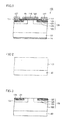
- a silicon carbide semiconductor device of the present embodiment is an MOSFET (Metal Oxide Semiconductor Field Effect Transistor) 100, specifically a vertical type DiMOSFET (Double Implanted MOSFET).
- MOSFET 100 includes a gate insulation film 126 (insulation film), an epitaxial layer 109 (silicon carbide layer), a single crystal substrate 80, a source electrode 111, an upper source electrode 127, a gate electrode 110, and a drain electrode 14.
- Epitaxial layer 109 includes a breakdown voltage holding layer 122, a p region 123, an n + region 124, and a p + region 125.
- Epitaxial layer 109 has a crystal structure of the hexagonal system.
- Epitaxial layer 109 includes a first region R1 at the surface.
- First region R1 has a first plane orientation at least partially.
- the first plane orientation is substantially any of the (0-33-8) plane, (30-3-8) plane, (-330-8) plane, (03-3-8) plane, (-303-8) plane, and (3-30-8) plane.
- the off orientation of the first plane orientation to the ⁇ 0001 ⁇ plane is within the range of ⁇ 5° to the ⁇ 1-100> direction.
- the off angle of the first plane orientation to the ⁇ 03-38 ⁇ plane in the ⁇ 1-100> direction is greater than or equal to - 3° and less than or equal to 3°.
- the inclination of the first plane orientation to the (000-1) plane is less than 90°.
- Single crystal substrate 80 is made of silicon carbide (SiC) and has n type conductivity.
- Breakdown voltage holding layer 122 is provided on single crystal substrate 80, and made of silicon carbide of n type conductivity.
- breakdown voltage holding layer 122 has a thickness of 10 ⁇ m, and the concentration of the n type conductive impurities is 5 ⁇ 10 15 cm -3 .
- p regions 123 At the surface of breakdown voltage holding layer 122 are provided a plurality of p regions 123 of p conductivity type, spaced apart from each other. In each p region 123, an n + region 124 is provided at the surface layer of p region 123. P region 123 constitutes first region R1 at the surface of epitaxial layer 109. The impurity concentration of p region 123 is selected in accordance with the threshold voltage of MOSFET 100.
- a p + region 125 is provided at the surface of breakdown voltage holding layer 122. P + region 125 is located adjacent to n + region 124.
- a gate insulation film 126 covering first region R1 is provided on breakdown voltage holding layer 122 exposed between adjacent p regions 123. Specifically, gate insulation film 126 extends from above n + region 124 at one of p regions 123, over the one p region 123, breakdown voltage holding layer 122, the other p region 123, as far as above n + region 124 at the other p region 123.
- a gate electrode 110 having a planar gate structure is provided on gate insulation film 126.
- a source electrode 111 is provided on n + region 124 and p + region 125. Upper source electrode 127 is provided on this source electrode 111.
- first region R 1 at the surface of epitaxial layer 109 and gate insulation film 126 has an interface state density below 5 ⁇ 10 11 cm -2 eV -1 .
- epitaxial layer 109 has channel mobility higher than or equal to 70 cm 2 /Vs on first region R1 at room temperature.
- p region 123 constituting first region R1 has an impurity concentration greater than or equal to 1 ⁇ 10 17 cm -3 on the surface.
- the silicon carbide semiconductor device may have a threshold value greater than or equal to 4V.
- epitaxial layer 109 may have channel mobility higher than or equal to 100 cm 2 /Vs on first region R1 at room temperature.
- p region 123 constituting first region R1 may have an impurity concentration greater than or equal to 2 ⁇ 10 16 cm -3 on the surface.
- the silicon carbide semiconductor device may have a threshold value greater than or equal to 2.5V.
- MOSFET 100 may have an S value less than or equal to 200 mV/decade. The definition of the S value will be provided afterwards.
- a method for manufacturing MOSFET 100 will be described hereinafter.
- epitaxial layer 109 is formed on single crystal substrate 80.
- the conductivity type and impurity concentration of epitaxial layer 109 are set identical to those of breakdown voltage holding layer 122 ( Fig. 1 ), for example.
- p region 123, n + region 124, and p + region 125 are formed. Specifically, implantation of impurity ions, followed by activation annealing are carried out. Activation annealing is carried out for 30 minutes at the heat temperature of 1700°C in an argon atmosphere, for example.
- gate insulation film 126 is formed so as to cover breakdown voltage holding layer 122, p region 123, and n + region 124 and p + region 125.
- This formation may be performed by thermal oxidation. Thermal oxidation is carried out by heating for 30 minutes at 1200°C in an oxidation atmosphere. Preferably, nitridation annealing is carried out thereafter. Specifically, annealing is carried out in nitric oxide (NO) atmosphere.
- the process conditions thereof include, for example, a heating temperature of 1100°C and a heating time of 120 minutes.
- a further annealing step using argon (Ar) gas that is inactive gas may be carried out.
- the process conditions thereof include, for example, a heating temperature of 1100°C and a heating time of 60 minutes.
- source electrode 111 and drain electrode 14 are formed.
- forming a nickel electrode and thermal treatment to obtain ohmic contact are carried out. This thermal treatment is carried out for 2 minutes at 950°C in inert gas, for example.
- an upper source electrode 127 is formed on source electrode 111.
- Gate electrode 110 is formed on gate insulation film 126.
- MOSFET 100 is obtained.
- epitaxial layer 109 may have high channel mobility on the surface covered with gate insulation film 126. This is due to first region R1 having the aforementioned first plane orientation at least partially.
- the interface between epitaxial layer 109 and gate insulation film 126 has an interface state density below 5 ⁇ 10 11 cm -2 eV -1 . Accordingly, higher channel mobility can be obtained more reliably.
- the silicon carbide semiconductor device may have an S value less than or equal to 200 mV/decade. Accordingly, a more rapid switching property can be achieved.
- the interface state density between first region R1 at the surface of epitaxial layer 109 and gate insulation film 126 can be further reduced.
- adsorption of nitrogen atoms to the interface can be made more firm.
- a silicon carbide semiconductor device of the present embodiment is an MOSFET 200, specifically a vertical type trench gate MOSFET.
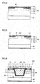
- MOSFET 200 includes a gate insulation film (insulation film), an epitaxial layer 209 (silicon carbide layer), a gate electrode 9, a single crystal substrate 80, a source electrode 12, a source interconnection electrode 13, and an interlayer insulation film 10.
- Epitaxial layer 209 includes a breakdown voltage holding layer 2 having n type conductivity, a p type body layer 3, an n type source contact layer 4, and a contact region 5 having p type conductivity.
- epitaxial layer 209 has a crystal structure of the hexagonal system.
- Epitaxial layer 209 includes a main surface TS substantially parallel to a main surface MS of single crystal substrate 80.
- Each of main surfaces MS and TS preferably has an off angle within 5° to the (000-1 plane).
- a trench 206 is provided on main surface TS.
- Trench 206 has side faces S1-S6 (first-sixth regions) as the surface of epitaxial layer 209.
- Trench 206 has a tapered shape increasing towards the opening, such that side faces S1-S6 are inclined relative to main surface TS.
- the region of side faces S1-S6 formed by p type body layer 3 constitutes the channel plane of MOSFET 200.
- Side faces S1-S6 have first to sixth plane orientations, respectively, at least partially, on p type body layer 3.
- the first to sixth plane orientations differ from each other.
- the first to sixth plane orientations are substantially any of the (0-33-8) plane, (30-3-8) plane, (-330-8) plane, (03-3-8) plane, (-303-8) plane, and (3-30-8) plane.
- the off orientation of the first to sixth plane orientations to the ⁇ 0001 ⁇ is within the range of ⁇ 5° to the ⁇ 1-100> direction.
- the off angle of the first to sixth plane orientations to the ⁇ 03-38 ⁇ plane in the ⁇ 1-100> direction is greater than or equal to - 3° and less than or equal to 3°.
- the inclination of the first to sixth plane orientations to the (000-1) plane is less than 90°.
- trench 206 corresponds to a mesa structure with main surface TS as the top face.
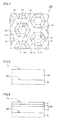
- the shape of this top face is a hexagon, as shown in Fig. 7 , in the case of hexagonal crystal.
- Breakdown voltage holding layer 2 is formed on one of the main surfaces of single crystal substrate 80.
- P type body layer 3 is formed on breakdown voltage holding layer 2.
- N type source contact layer 4 is formed on p type body layer 3.
- P type contact region 5 is formed so as to be surrounded by n type source contact layer 4.
- Gate insulation film 8 is formed on side faces S1-S6 and the bottom face of trench 206. This gate insulation film 8 extends as far as the upper face of n type source contact layer 4. Gate electrode 9 is formed on gate insulation film 8, such that the interior of trench 206 is filled (that is, to fill the space between adjacent mesa structures). In other words, gate electrode 9 constitutes a trench gate structure.
- the upper face of gate electrode 9 is substantially equal in height with the top face of gate insulation film 8 at the region located above the upper surface of n type source contact layer 4.
- Interlayer insulation film 10 is formed to cover the portion of gate insulation film 8 extending as far as above the upper face of n type source contact layer 4 and gate electrode 9. By removing interlayer insulation film 10 and a portion of gate insulation film 8, an opening 11 is formed so as to expose a portion of n type source contact layer 4 and p type contact region 5.
- Source electrode 12 is formed to fill the interior of opening 11, and in contact with p type contact region 5 and a portion of n type source contact layer 4.
- Source interconnection electrode 13 is formed to be brought into contact with the upper face of source electrode 12, and to extend on the upper face of interlayer insulation film 10.
- Drain electrode 14 is formed on the back face of single crystal substrate 80, opposite to the main surface where breakdown voltage holding layer 2 is formed. Drain electrode 14 is an ohmic electrode.
- MOSFET 200 The method for manufacturing MOSFET 200 will be described hereinafter.
- epitaxial layer 209 having main surface TS is formed on single crystal substrate 80.
- epitaxial layer 209 of n conductivity type is formed.
- This epitaxial growth can be executed by CVD (Chemical Vapor Deposition) using mixture gas of silane (SiH 4 ) and propane (C 3 H 8 ) as raw material gas and using hydrogen gas (H 2 ), for example, as the carrier gas.
- SiH 4 silane
- propane C 3 H 8
- H 2 hydrogen gas
- nitrogen (N) or phosphorus (P) is preferably introduced as impurities for epitaxial layer 209 to be doped n-type.
- the impurity concentration can be set greater than or equal to 5 ⁇ 10 15 cm -3 and less than or equal to 5 ⁇ 10 16 cm -3 , for example.
- breakdown voltage holding layer 2 As shown in Fig. 9 , breakdown voltage holding layer 2, p type body layer 3 and n type source contact layer 4 are formed on epitaxial layer 209. Specifically, by implanting ions to the upper face layer of epitaxial layer 209, p type body layer 3 and n type source contact layer 4 are formed, and the region not having ions implanted becomes breakdown voltage holding layer 2. As to ion implantation for forming p type body layer 3, impurity ions such as aluminium (Al) are implanted to render p-type. At this stage, the depth of the region where p type body layer 3 is formed can be adjusted by regulating the acceleration energy of implanted ions.
- Al aluminium
- n type source contact layer 4 is formed.
- Impurities for rendering the n-type include phosphorus (P), for example.
- a mask 17 is formed to cover a portion of main surface TS of epitaxial layer 209.
- an insulation film such as a silicon oxide film can be used.
- Mask 17 can be formed by a method including the steps set forth below, by way of example.
- a silicon oxide film is formed by CVD or the like on the upper face of n type source contact layer 4.
- a resist film (not shown) having a predetermined opening pattern is formed by photolithography on the silicon oxide film.
- the silicon oxide film is removed by etching.
- the resist film is removed.
- mask 17 having an opening pattern is formed.
- a recess 16 is formed having a sidewall substantially perpendicular to main surface TS of single crystal substrate 80.
- mask 17 is used to etch n type source contact layer 4, p type body layer 3, and a portion of breakdown voltage holding layer 2.
- RIE reactive ion etching
- ICP inductively coupled plasma
- ICP-RIE ICP-RIE using SF 6 or a mixture gas of SF 6 and O 2 as reactive gas can be employed.
- a trench 206 is formed such that sidewalls S1-S6 inclined relative to main surface TS are provided at epitaxial layer 209.
- main surface TS of epitaxial layer 209 having mask 17 formed is subjected to thermal etching.
- thermal etching is carried out by means of chemical reaction that occurs by supplying process gas including reactive gas to an etching subject that is heated.
- chlorine based gas preferably chlorine gas
- thermal etching is carried out preferably in an atmosphere in which the partial pressure of the chlorine based gas is less than or equal to 50%. Thermal etching is carried out in an atmosphere preferably under reduced pressure.
- the atmosphere for etching has reduced pressure less than or equal to 1/10 the atmospheric pressure.
- thermal etching is preferably carried out under the condition where the temperature of single crystal substrate 80 having epitaxial layer 209 provided (thermal treatment temperature) is greater than or equal to 1000°C.
- Etching is carried out using a mixture gas of oxygen gas and chlorine gas as the reaction gas for the process gas, and at a thermal treatment temperature greater than or equal to 700°C and less than or equal to 1200°C.
- the thermal treatment temperature is preferably greater than or equal to 700°C and less than or equal to 200°C.
- a quartz member can be employed for the device directed to thermal treatment.
- the upper limit of the temperature is more preferably 1100°C, further more preferably 1000°C.
- the lower limit of the temperature is more preferably 800°C, further more preferably 900°C. In this case, the etching rate can take a value sufficiently practical.
- the main reaction proceeds when the conditions of 0.5 ⁇ x ⁇ 2.0 and 1.0 ⁇ y ⁇ 2.0 are satisfied for x and y in the reaction formula represented by SiC + mO 2 + nCl 2 ⁇ SiCl x + CO y (where m, n, x and y are positive numbers).
- the aforementioned m and n represent the amount of oxygen gas and chlorine gas actually reacting, and do not represent the amount supplied as the process gas.
- the rate of the flow rate of oxygen to the flow rate of chlorine supplied in this thermal etching is preferably greater than or equal to 0.1 and less than or equal to 2.0. More preferably, the lower limit of this rate is 0.25.
- the reaction gas may include carrier gas, in addition to the aforementioned chlorine gas and oxygen gas.
- carrier gas nitrogen (N 2 ) gas, argon gas, helium gas, or the like may be used by way of example.
- N 2 nitrogen
- argon gas argon gas
- helium gas or the like may be used by way of example.
- the thermal treatment temperature is greater than or equal to 700°C and less than or equal to 1000°C, as set forth above, the etching rate of SiC becomes approximately 70 ⁇ m/hr, for example.
- silicon oxide (SiO 2 ) is used for mask 17, the selected ratio of SiC to SiO 2 can be set significantly great. Therefore, mask 17 formed of SiO 2 substantially will not be etched during SiC etching.
- mask 17 is removed by an arbitrary method such as by etching.
- contact region 5 is formed.
- the plane shape of trench 206 constitutes a mesh formed with each unitary cell (annular trench 206 surrounding one mesa structure) taking a hexagonal shape.
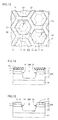
- P type contact region 5 is arranged substantially at the central region of the upper face of the mesa structure, as shown in Fig. 16 .
- the plane shape of p type contact region 5 is identical to the outer circumferential shape of the upper face of the mesa structure, i.e. a hexagonal shape.
- the step of activation annealing is performed to render active the impurities implanted by ion-implantation set forth above.
- the surface of the epitaxial layer made of silicon carbide (for example, the sidewall of the mesa structure) is subjected to annealing without particularly forming a cap layer.
- activation annealing may be performed with the aforementioned cap layer formed.
- activation annealing may be performed based on a configuration in which a cap layer is provided only on the upper face of n type source contact layer 4 and p type contact region 5.
- gate insulation film 8 is formed on side faces S1-S6 of epitaxial layer 209. Specifically, gate insulation film 8 is formed, extending from the interior of trench 206 and as far as above the upper face of n type source contact layer 4 and p type contact region 5.
- an oxide film (silicon oxide film) obtained by applying thermal oxidation to epitaxial layer 209, for example, can be employed.
- gate electrode 9 is formed facing each of side faces S1-S6 of epitaxial layer 209 with gate insulation film 8 therebetween. Specifically, gate electrode 9 is formed on gate insulation film 8 so as to fill the interior of trench 206. Gate electrode 9 can be formed by the method set forth below. First, a conductor film to become a gate electrode is formed by sputtering or the like on gate insulation film 8, inside trench 206 and extending as far as the region above p type contact region 5. For the material of the conductor film, any arbitrary material such as metal can be used as long as the material has conductivity.
- interlayer insulation film 10 is formed to cover the upper face of gate electrode 9, and the upper face of gate insulation film 8 exposed at p type contact region 5.
- any arbitrary material may be employed as long as the material has insulation.
- a resist film (not shown) having a pattern is formed by photolithography on interlayer insulation film 10.
- the resist film has an opening pattern formed at the region located on p type contact region 5.
- interlayer insulation film 10 and gate insulation film 8 are partially removed by etching.
- an opening 11 (refer to Fig. 19 ) is formed in interlayer insulation film 10 and gate insulation film 8. Under this state, p type contact region 5 and a portion of n type source contact layer 4 are exposed at the bottom of opening 11.
- Source electrode 12 is formed by the conductor film in opening 11.
- Source electrode 12 is an ohmic electrode establishing an ohmic contact with p type contact region 5 and n type source contact layer 4.
- Drain electrode 14 is formed at the backside of single crystal substrate 80 (the surface side opposite to the main surface where breakdown voltage holding layer 2 is formed).
- an arbitrary material can be employed as long as it is capable of forming an ohmic contact with single crystal substrate 80.
- source interconnection electrode 13 is formed by an arbitrary method such as sputtering in contact with the upper face of source electrode 12 and extending on the upper face of interlayer insulation film 10.
- MOSFET 200 is obtained.
- the channel mobility can be increased at MOSFET 200 having a hexagonal shape as the plane pattern (refer to Fig. 7 ).
- trench 206 of MOSFET 200 has a flat bottom plane
- a V-shape trench may be formed, such as trench 206V ( Fig. 2 ) of MOSFET 200v.
- the MOSFET can be further integrated.
- a silicon carbide semiconductor device of the present embodiment is an MOSFET 300, which is a vertical type trench gate MOSFET, likewise with MOSFET 200 of the second embodiment.
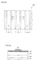
- MOSFET 300 has an epitaxial layer 309 differing from epitaxial layer 209 ( Fig. 7 ) of MOSFET 200, and includes a trench 306 taking a stripe shape in plan view, as shown in Fig. 22 .
- Trench 306 includes side faces T1 and T2 (first and second regions) as the surface of epitaxial layer 309.
- Trench 306 has a tapered configuration increasing towards the opening. Therefore, side faces T1 and T2 are inclined relative to main surface TS.
- the region of side faces T1 and T2 formed by p type body layer 3 constitutes the channel plane of MOSFET 300.
- Side faces T1 and T2 have first and second plane orientations, respectively, on p type body layer 3, at least partially.
- the first and second plane orientations differ from each other.
- the first and second plane orientations are substantially any of the (0-33-8) plane, (30-3-8) plane, (-330-8) plane, (03-3-8) plane, (-303-8) plane and (3-30-8) plane.
- the off orientation of the first and second plane orientations to the ⁇ 0001 ⁇ plane is within the range of ⁇ 5° to the ⁇ 1-100> direction.
- the off angle of the first and second plane orientations to the ⁇ 03-38 ⁇ plane in the ⁇ 1-100> direction is greater than or equal to - 3° and less than or equal to 3°
- the inclination of the first to sixth plane orientations to the (000-1) plane is less than 90°.
- the first plane is substantially the (0-33-8) plane and the second plane is substantially the (03-3-8) plane.
- two different planes having high channel mobility can be provided.
- the channel mobility can be increased at MOSFET 300 having the shape of stripes as a plane pattern (refer to Fig. 22 ).
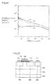
- a MOS capacitor was produced using a silicon carbide substrate including a top face having a plane orientation of the (0-33-8) plane.
- a MOS capacitor was produced using a silicon carbide substrate including a top face having a plane orientation of the (03-38) plane.
- a MOS capacitor was produced using a silicon carbide substrate including a top face having a plane orientation of the (0001) plane.
- n type silicon carbide substrate 402 was prepared.
- An n type SiC layer 403 was formed on the top face of silicon carbide substrate 402 by epitaxial growth.
- n type SiC layer 403 was formed on the top face of silicon carbide substrate 402 by epitaxial growth.
- a gate oxide film 404 SiO 2
- annealing was carried out. Specifically, a first annealing in a NO atmosphere and a second annealing in an Ar atmosphere were carried out. Each of the first and second annealing was carried out at the annealing temperature of 1250°C, and annealing time of 1 hour.
- gate electrode 405 was formed on the gate oxide film by Al deposition.
- gate electrode 405 was set to 300-500 ⁇ m ⁇ . Also, a contact electrode 401 (Body) was formed on the backside of silicon carbide substrate 402. Specifically, Ni deposition and RTA at 1000°C in an Ar atmosphere for 2 minutes were carried out.
- the interface state density was lower for the (0-33-8) plane than for the (03-38) plane.
- the difference was significant under energy values that were at shallow level from the conduction electron band.
- the interface state density on the (0-33-8) plane was lower as compared to that on the (03-38) plane or the (0001) plane.
- it is estimated that a more favorable interface is formed on the (0-33-8) plane.
- Each of the (30-3-8) plane, (-330-8) plane, (03-3-8) plane, (-303-8) plane and (3-30-8) plane is equivalent to the (0-33-8) plane from the standpoint of the physical properties set forth above.
- an MOSFET was produced using a silicon carbide substrate including a top face having a plane orientation of the (0-33-8) plane. Specifically, an MOSFET having the source/drain arranged in a direction parallel to the [11-20] direction (Example 1), and an MOSFET having the source/drain arranged in a direction perpendicular to the [11-20] direction (Example 2) were produced. For a comparative example, an MOSFET was produced using a silicon carbide substrate including a top face having a plane orientation of the (03-38) plane.
- an MOSFET having the source/drain arranged in a direction parallel to the [11-20] direction (Comparative Example 1) and an MOSFET having the source/drain arranged in a direction perpendicular to the [11-20] direction (Comparative Example 2) were produced.
- An n type SiC layer 502 was formed by epitaxial growth on the top face of n type SiC substrate 501. Al ions were implanted onto n type SiC layer 502 to form a p well layer 503. The impurity concentration and the depth of p well layer 503 were set to approximately 2 ⁇ 10 16 cm -3 and approximately 700 nm, respectively.
- an n + source region 504, an n + drain region 505, and a p + body region 506 were formed in p well layer 503. The regions were doped p type and n type using Al ions and P ions, respectively. Then, a cap was formed.
- Activation annealing was carried out for 20 minutes at 1700°C in an Ar atmosphere. Then, the epitaxial surface was cleaned by sacrificial oxidation. Next, a gate oxide film 507 (SiO 2 ) was formed, followed by annealing thereof. Specifically, a first annealing in NO atmosphere and a second annealing in an Ar atmosphere were carried out on gate oxide film 507. Each annealing was carried out at the temperature of 1250°C and for 1 hour. Then, Ni deposition and RTA at 1000°C in an Ar atmosphere for 2 minutes were carried out on each of n + source region 504, n + drain region 505 and p + body region 506. Furthermore, Al deposition was carried out on each of these regions. Accordingly, a source electrode 509, a drain electrode 510, and a body electrode 511 were formed. Further, a gate electrode 508 was formed by Al deposition on gate oxide film 507.
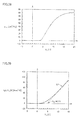
- each ⁇ fe-max of Examples 1 and 2 was greater than that of each of Comparative Examples 1 and 2.
- the graph in each of Figs. 26 and 27 indicates the drain current I D to the gate voltage V G in Examples 1 and 2.
- the vertical axis at the left side is based on the log scale.
- the vertical axis at the right side is based on a linear scale and has a coefficient L/C OX W applied.
- L indicates the channel length, which was set at 100 ⁇ m.
- W indicates the channel width, which was set at 200 ⁇ m.
- C OX indicates the capacitance of gate oxide film 507.
- Each of the (30-3-8) plane, (-330-8) plane, (03-3-8) plane, (-303-8) plane and (3-30-8) plane is equivalent to the (0-33-8) plane from the standpoint of physical properties set forth above.
- the impurity concentration of p well layer 503 in Examples 1 and 2 was set to approximately 2 ⁇ 10 16 cm -3
- the threshold value of gate voltage V G could be set greater than or equal to 2.5V even if the impurity concentration was reduced as low as 1 ⁇ 10 16 cm -3 .
- the impurity concentration of p well layer 503, i.e. the impurity concentration of the channel was set to approximately 2 ⁇ 10 16 cm -3 .
- the impurity concentration was set to 1 ⁇ 10 17 cm -3 .
- the remaining conditions are substantially similar to those of the examples set forth above. From the measured results of channel mobility ⁇ fe of Example 3 ( Fig. 28 ) when the drain voltage V D was set at 0.1V, the maximum channel mobility ⁇ fe-max was higher than or equal to 70 cm 2 /Vs.
- the threshold voltage V th was 4.5V.
- Threshold voltage V th in the present specification was obtained by carrying out approximation by linear function to the linear increase region LP of I D L/C OX W, as shown in Fig. 29 , and using the crossing point between this function and the V G axis. Details of the method for calculating this V th will be described hereinafter.
- Drain current I D is represented by the following equation (1), where ⁇ is the channel mobility and V D is the drain voltage.
- I D ⁇ WC ox ⁇ V D ⁇ V G - V D / 2 - V th / L
- Equation (2) is a linear function with V G as a variable.
- the portion represented by this function corresponds to the linear increase region LP ( Fig. 29 ).
- V G X
- V th X - V D /2
- threshold voltage V th can be obtained.
- S value is also referred to as the subthreshold coefficient.
- the S values of Examples 1 and 2 were both less than 200 mV/decade, which are significantly lower than the S values of Comparative Examples 1 and 2. It is therefore appreciated that a silicon carbide semiconductor device having a rapid switching property can be obtained by using the (0-33-8) plane corresponding to Examples 1 and 2 as the channel.
- Each of the (30-3-8) plane, (-330-8) plane, (03-3-8) plane, (-303-8) plane and (3-30-8) plane is equivalent to the (0-33-8) plane from the standpoint of the physical properties set forth above.
- the differential of Equation (3) corresponds to the region where log 10 I D increases linearly in accordance with the increase of gate voltage V G (subthreshold slope SS in Fig. 30 ).
- the value is calculated based on the average from the data in 0.1 V steps in the range of V th ⁇ V G ⁇ V th + 0.3 (V), for example.
- the surface of the silicon carbide layer may have a region (for example, side face S1 of Fig. 6 as the first region) constituted of a composite plane CP ( Fig. 31 ) having a specific plane orientation partially.
- a specific plane orientation is any of the (0-33-8) plane, (30-3-8) plane, (-330-8) plane, (03-3-8) plane, (-303-8) plane and (3-30-8) plane.
- a composite plane CP includes a first portion P1 formed of a first plane and a second portion R2 formed of another plane differing from the first plane, when viewed microscopically.
- each of first and second portions P1 and P2 may have a width dimension approximately two times the interatomic spacing in the aligning direction of adjacent first and second portions P1 and P2 (periodic direction), and a dimension sufficiently greater than the interatomic spacing in the direction crossing the periodic direction.
Landscapes
- Insulated Gate Type Field-Effect Transistor (AREA)
- Electrodes Of Semiconductors (AREA)
Applications Claiming Priority (3)
| Application Number | Priority Date | Filing Date | Title |
|---|---|---|---|
| US201261593681P | 2012-02-01 | 2012-02-01 | |
| JP2012036988A JP6119100B2 (ja) | 2012-02-01 | 2012-02-23 | 炭化珪素半導体装置 |
| PCT/JP2012/082493 WO2013114743A1 (ja) | 2012-02-01 | 2012-12-14 | 炭化珪素半導体装置 |
Publications (3)
| Publication Number | Publication Date |
|---|---|
| EP2811529A1 true EP2811529A1 (de) | 2014-12-10 |
| EP2811529A4 EP2811529A4 (de) | 2015-07-08 |
| EP2811529B1 EP2811529B1 (de) | 2019-12-04 |
Family
ID=49174085
Family Applications (1)
| Application Number | Title | Priority Date | Filing Date |
|---|---|---|---|
| EP12867527.9A Active EP2811529B1 (de) | 2012-02-01 | 2012-12-14 | Halbleiterbauelement aus siliciumcarbid |
Country Status (5)
| Country | Link |
|---|---|
| US (1) | US8829535B2 (de) |
| EP (1) | EP2811529B1 (de) |
| JP (1) | JP6119100B2 (de) |
| CN (1) | CN104025300B (de) |
| WO (1) | WO2013114743A1 (de) |
Families Citing this family (9)
| Publication number | Priority date | Publication date | Assignee | Title |
|---|---|---|---|---|
| JP5954140B2 (ja) * | 2012-11-29 | 2016-07-20 | 住友電気工業株式会社 | 炭化珪素半導体装置 |
| JP6183080B2 (ja) * | 2013-09-09 | 2017-08-23 | 住友電気工業株式会社 | 炭化珪素半導体装置およびその製造方法 |
| JP2015056544A (ja) * | 2013-09-12 | 2015-03-23 | 住友電気工業株式会社 | 炭化珪素半導体装置およびその製造方法 |
| JP6294208B2 (ja) * | 2014-10-17 | 2018-03-14 | トヨタ自動車株式会社 | トレンチゲート電極を有する絶縁ゲート型スイッチング素子の製造方法 |
| JP7166053B2 (ja) | 2017-12-21 | 2022-11-07 | 株式会社東芝 | 半導体装置、インバータ回路、駆動装置、車両、及び、昇降機 |
| CN111403280A (zh) * | 2020-03-31 | 2020-07-10 | 中国科学院微电子研究所 | 一种碳化硅mos电容器件及其制作方法 |
| JP7697210B2 (ja) | 2021-01-21 | 2025-06-24 | 富士電機株式会社 | 炭化珪素半導体装置および炭化珪素半導体装置の製造方法 |
| CN114843185A (zh) * | 2021-02-02 | 2022-08-02 | 中国科学院微电子研究所 | 一种碳化硅器件的制备方法 |
| WO2025197966A1 (ja) * | 2024-03-21 | 2025-09-25 | 株式会社Power Diamond Systems | ダイヤモンド半導体装置およびダイヤモンド半導体装置の製造方法 |
Family Cites Families (16)
| Publication number | Priority date | Publication date | Assignee | Title |
|---|---|---|---|---|
| US6057558A (en) * | 1997-03-05 | 2000-05-02 | Denson Corporation | Silicon carbide semiconductor device and manufacturing method thereof |
| JP3610721B2 (ja) * | 1997-03-05 | 2005-01-19 | 株式会社デンソー | 炭化珪素半導体装置 |
| JP4581270B2 (ja) | 2001-03-05 | 2010-11-17 | 住友電気工業株式会社 | SiC半導体のイオン注入層及びその製造方法 |
| JP4843854B2 (ja) | 2001-03-05 | 2011-12-21 | 住友電気工業株式会社 | Mosデバイス |
| JP5017768B2 (ja) * | 2004-05-31 | 2012-09-05 | 富士電機株式会社 | 炭化珪素半導体素子 |
| JP5017855B2 (ja) * | 2005-12-14 | 2012-09-05 | 富士電機株式会社 | 半導体装置の製造方法 |
| WO2011092808A1 (ja) * | 2010-01-27 | 2011-08-04 | 住友電気工業株式会社 | 炭化ケイ素半導体装置およびその製造方法 |
| JP2010192697A (ja) * | 2009-02-18 | 2010-09-02 | Sumitomo Electric Ind Ltd | 炭化珪素基板および炭化珪素基板の製造方法 |
| TW201044586A (en) * | 2009-03-27 | 2010-12-16 | Sumitomo Electric Industries | Mosfet and method for manufacturing mosfet |
| WO2010110252A1 (ja) * | 2009-03-27 | 2010-09-30 | 住友電気工業株式会社 | Mosfetおよびmosfetの製造方法 |
| JPWO2010116887A1 (ja) * | 2009-04-10 | 2012-10-18 | 住友電気工業株式会社 | 絶縁ゲート型電界効果トランジスタ |
| CN102422425A (zh) | 2009-05-11 | 2012-04-18 | 住友电气工业株式会社 | 绝缘栅双极晶体管 |
| CA2764900A1 (en) * | 2009-10-30 | 2011-05-05 | Sumitomo Electric Industries, Ltd. | Method for manufacturing silicon carbide substrate and silicon carbide substrate |
| EP3869537A1 (de) * | 2010-03-23 | 2021-08-25 | Sumitomo Electric Industries, Ltd. | Halbleiterbauelement und verfahren zur herstellung davon |
| JP2011233669A (ja) * | 2010-04-27 | 2011-11-17 | Sumitomo Electric Ind Ltd | 半導体装置 |
| JP2012004494A (ja) * | 2010-06-21 | 2012-01-05 | Sumitomo Electric Ind Ltd | 炭化珪素基板の製造方法および製造装置 |
-
2012
- 2012-02-23 JP JP2012036988A patent/JP6119100B2/ja active Active
- 2012-12-14 EP EP12867527.9A patent/EP2811529B1/de active Active
- 2012-12-14 CN CN201280065718.8A patent/CN104025300B/zh active Active
- 2012-12-14 WO PCT/JP2012/082493 patent/WO2013114743A1/ja not_active Ceased
- 2012-12-20 US US13/722,486 patent/US8829535B2/en active Active
Also Published As
| Publication number | Publication date |
|---|---|
| WO2013114743A1 (ja) | 2013-08-08 |
| CN104025300B (zh) | 2017-02-22 |
| CN104025300A (zh) | 2014-09-03 |
| US20130193447A1 (en) | 2013-08-01 |
| EP2811529A4 (de) | 2015-07-08 |
| JP2013162118A (ja) | 2013-08-19 |
| US8829535B2 (en) | 2014-09-09 |
| EP2811529B1 (de) | 2019-12-04 |
| JP6119100B2 (ja) | 2017-04-26 |
Similar Documents
| Publication | Publication Date | Title |
|---|---|---|
| EP2811529B1 (de) | Halbleiterbauelement aus siliciumcarbid | |
| US8803252B2 (en) | Silicon carbide semiconductor device | |
| US10756188B2 (en) | Silicon carbide semiconductor device and method of manufacturing the same | |
| CN103069571B (zh) | 碳化硅半导体元件及其制造方法 | |
| US9054022B2 (en) | Method for manufacturing semiconductor device | |
| US9276106B2 (en) | Silicon carbide semiconductor device and method for manufacturing same | |
| US20170117381A1 (en) | Semiconductor device and method for manufacturing same | |
| US9012922B2 (en) | Silicon carbide semiconductor device and method for manufacturing same | |
| US11784217B2 (en) | Silicon carbide semiconductor device | |
| US9608074B2 (en) | Silicon carbide semiconductor device and method for manufacturing silicon carbide semiconductor device | |
| CA2766981A1 (en) | Silicon carbide insulating gate type semiconductor device and fabrication method thereof | |
| US8999854B2 (en) | Method for manufacturing silicon carbide semiconductor device | |
| US20140252374A1 (en) | Silicon carbide semiconductor device | |
| US20170207311A1 (en) | Silicon carbide semiconductor device and method for manufacturing same | |
| US20160126347A1 (en) | Silicon carbide semiconductor device | |
| US10192967B2 (en) | Silicon carbide semiconductor with trench gate | |
| US20130119407A1 (en) | Method for manufacturing semiconductor device, and semiconductor device | |
| US20130221375A1 (en) | Silicon carbide semiconductor device and method for manufacturing same | |
| EP2851957B1 (de) | Halbleiterbauelement aus siliciumcarbid | |
| US9893177B2 (en) | Silicon carbide semiconductor device and method of manufacturing the same | |
| US20130306987A1 (en) | Silicon carbide semiconductor device and method for manufacturing same |
Legal Events
| Date | Code | Title | Description |
|---|---|---|---|
| PUAI | Public reference made under article 153(3) epc to a published international application that has entered the european phase |
Free format text: ORIGINAL CODE: 0009012 |
|
| 17P | Request for examination filed |
Effective date: 20140521 |
|
| AK | Designated contracting states |
Kind code of ref document: A1 Designated state(s): AL AT BE BG CH CY CZ DE DK EE ES FI FR GB GR HR HU IE IS IT LI LT LU LV MC MK MT NL NO PL PT RO RS SE SI SK SM TR |
|
| AX | Request for extension of the european patent |
Extension state: BA ME |
|
| DAX | Request for extension of the european patent (deleted) | ||
| RA4 | Supplementary search report drawn up and despatched (corrected) |
Effective date: 20150609 |
|
| RIC1 | Information provided on ipc code assigned before grant |
Ipc: H01L 21/336 20060101ALI20150602BHEP Ipc: H01L 29/78 20060101AFI20150602BHEP Ipc: H01L 29/12 20060101ALI20150602BHEP Ipc: H01L 29/04 20060101ALI20150602BHEP |
|
| STAA | Information on the status of an ep patent application or granted ep patent |
Free format text: STATUS: EXAMINATION IS IN PROGRESS |
|
| 17Q | First examination report despatched |
Effective date: 20171016 |
|
| GRAP | Despatch of communication of intention to grant a patent |
Free format text: ORIGINAL CODE: EPIDOSNIGR1 |
|
| STAA | Information on the status of an ep patent application or granted ep patent |
Free format text: STATUS: GRANT OF PATENT IS INTENDED |
|
| RIC1 | Information provided on ipc code assigned before grant |
Ipc: H01L 29/04 20060101ALI20190605BHEP Ipc: H01L 29/423 20060101ALI20190605BHEP Ipc: H01L 29/78 20060101AFI20190605BHEP Ipc: H01L 29/12 20060101ALI20190605BHEP |
|
| INTG | Intention to grant announced |
Effective date: 20190628 |
|
| GRAS | Grant fee paid |
Free format text: ORIGINAL CODE: EPIDOSNIGR3 |
|
| GRAA | (expected) grant |
Free format text: ORIGINAL CODE: 0009210 |
|
| STAA | Information on the status of an ep patent application or granted ep patent |
Free format text: STATUS: THE PATENT HAS BEEN GRANTED |
|
| AK | Designated contracting states |
Kind code of ref document: B1 Designated state(s): AL AT BE BG CH CY CZ DE DK EE ES FI FR GB GR HR HU IE IS IT LI LT LU LV MC MK MT NL NO PL PT RO RS SE SI SK SM TR |
|
| REG | Reference to a national code |
Ref country code: GB Ref legal event code: FG4D |
|
| REG | Reference to a national code |
Ref country code: CH Ref legal event code: EP |
|
| REG | Reference to a national code |
Ref country code: AT Ref legal event code: REF Ref document number: 1210485 Country of ref document: AT Kind code of ref document: T Effective date: 20191215 |
|
| REG | Reference to a national code |
Ref country code: DE Ref legal event code: R096 Ref document number: 602012066289 Country of ref document: DE |
|
| REG | Reference to a national code |
Ref country code: IE Ref legal event code: FG4D |
|
| REG | Reference to a national code |
Ref country code: NL Ref legal event code: MP Effective date: 20191204 |
|
| REG | Reference to a national code |
Ref country code: LT Ref legal event code: MG4D |
|
| PG25 | Lapsed in a contracting state [announced via postgrant information from national office to epo] |
Ref country code: ES Free format text: LAPSE BECAUSE OF FAILURE TO SUBMIT A TRANSLATION OF THE DESCRIPTION OR TO PAY THE FEE WITHIN THE PRESCRIBED TIME-LIMIT Effective date: 20191204 Ref country code: NO Free format text: LAPSE BECAUSE OF FAILURE TO SUBMIT A TRANSLATION OF THE DESCRIPTION OR TO PAY THE FEE WITHIN THE PRESCRIBED TIME-LIMIT Effective date: 20200304 Ref country code: GR Free format text: LAPSE BECAUSE OF FAILURE TO SUBMIT A TRANSLATION OF THE DESCRIPTION OR TO PAY THE FEE WITHIN THE PRESCRIBED TIME-LIMIT Effective date: 20200305 Ref country code: BG Free format text: LAPSE BECAUSE OF FAILURE TO SUBMIT A TRANSLATION OF THE DESCRIPTION OR TO PAY THE FEE WITHIN THE PRESCRIBED TIME-LIMIT Effective date: 20200304 Ref country code: FI Free format text: LAPSE BECAUSE OF FAILURE TO SUBMIT A TRANSLATION OF THE DESCRIPTION OR TO PAY THE FEE WITHIN THE PRESCRIBED TIME-LIMIT Effective date: 20191204 Ref country code: LT Free format text: LAPSE BECAUSE OF FAILURE TO SUBMIT A TRANSLATION OF THE DESCRIPTION OR TO PAY THE FEE WITHIN THE PRESCRIBED TIME-LIMIT Effective date: 20191204 Ref country code: SE Free format text: LAPSE BECAUSE OF FAILURE TO SUBMIT A TRANSLATION OF THE DESCRIPTION OR TO PAY THE FEE WITHIN THE PRESCRIBED TIME-LIMIT Effective date: 20191204 Ref country code: LV Free format text: LAPSE BECAUSE OF FAILURE TO SUBMIT A TRANSLATION OF THE DESCRIPTION OR TO PAY THE FEE WITHIN THE PRESCRIBED TIME-LIMIT Effective date: 20191204 |
|
| PG25 | Lapsed in a contracting state [announced via postgrant information from national office to epo] |
Ref country code: HR Free format text: LAPSE BECAUSE OF FAILURE TO SUBMIT A TRANSLATION OF THE DESCRIPTION OR TO PAY THE FEE WITHIN THE PRESCRIBED TIME-LIMIT Effective date: 20191204 Ref country code: RS Free format text: LAPSE BECAUSE OF FAILURE TO SUBMIT A TRANSLATION OF THE DESCRIPTION OR TO PAY THE FEE WITHIN THE PRESCRIBED TIME-LIMIT Effective date: 20191204 |
|
| PG25 | Lapsed in a contracting state [announced via postgrant information from national office to epo] |
Ref country code: AL Free format text: LAPSE BECAUSE OF FAILURE TO SUBMIT A TRANSLATION OF THE DESCRIPTION OR TO PAY THE FEE WITHIN THE PRESCRIBED TIME-LIMIT Effective date: 20191204 |
|
| PG25 | Lapsed in a contracting state [announced via postgrant information from national office to epo] |
Ref country code: RO Free format text: LAPSE BECAUSE OF FAILURE TO SUBMIT A TRANSLATION OF THE DESCRIPTION OR TO PAY THE FEE WITHIN THE PRESCRIBED TIME-LIMIT Effective date: 20191204 Ref country code: CZ Free format text: LAPSE BECAUSE OF FAILURE TO SUBMIT A TRANSLATION OF THE DESCRIPTION OR TO PAY THE FEE WITHIN THE PRESCRIBED TIME-LIMIT Effective date: 20191204 Ref country code: NL Free format text: LAPSE BECAUSE OF FAILURE TO SUBMIT A TRANSLATION OF THE DESCRIPTION OR TO PAY THE FEE WITHIN THE PRESCRIBED TIME-LIMIT Effective date: 20191204 Ref country code: PT Free format text: LAPSE BECAUSE OF FAILURE TO SUBMIT A TRANSLATION OF THE DESCRIPTION OR TO PAY THE FEE WITHIN THE PRESCRIBED TIME-LIMIT Effective date: 20200429 Ref country code: EE Free format text: LAPSE BECAUSE OF FAILURE TO SUBMIT A TRANSLATION OF THE DESCRIPTION OR TO PAY THE FEE WITHIN THE PRESCRIBED TIME-LIMIT Effective date: 20191204 |
|
| REG | Reference to a national code |
Ref country code: CH Ref legal event code: PL |
|
| REG | Reference to a national code |
Ref country code: BE Ref legal event code: MM Effective date: 20191231 |
|
| PG25 | Lapsed in a contracting state [announced via postgrant information from national office to epo] |
Ref country code: SM Free format text: LAPSE BECAUSE OF FAILURE TO SUBMIT A TRANSLATION OF THE DESCRIPTION OR TO PAY THE FEE WITHIN THE PRESCRIBED TIME-LIMIT Effective date: 20191204 Ref country code: IS Free format text: LAPSE BECAUSE OF FAILURE TO SUBMIT A TRANSLATION OF THE DESCRIPTION OR TO PAY THE FEE WITHIN THE PRESCRIBED TIME-LIMIT Effective date: 20200404 Ref country code: SK Free format text: LAPSE BECAUSE OF FAILURE TO SUBMIT A TRANSLATION OF THE DESCRIPTION OR TO PAY THE FEE WITHIN THE PRESCRIBED TIME-LIMIT Effective date: 20191204 |
|
| REG | Reference to a national code |
Ref country code: DE Ref legal event code: R097 Ref document number: 602012066289 Country of ref document: DE |
|
| REG | Reference to a national code |
Ref country code: AT Ref legal event code: MK05 Ref document number: 1210485 Country of ref document: AT Kind code of ref document: T Effective date: 20191204 |
|
| PG25 | Lapsed in a contracting state [announced via postgrant information from national office to epo] |
Ref country code: MC Free format text: LAPSE BECAUSE OF FAILURE TO SUBMIT A TRANSLATION OF THE DESCRIPTION OR TO PAY THE FEE WITHIN THE PRESCRIBED TIME-LIMIT Effective date: 20191204 |
|
| PLBE | No opposition filed within time limit |
Free format text: ORIGINAL CODE: 0009261 |
|
| STAA | Information on the status of an ep patent application or granted ep patent |
Free format text: STATUS: NO OPPOSITION FILED WITHIN TIME LIMIT |
|
| PG25 | Lapsed in a contracting state [announced via postgrant information from national office to epo] |
Ref country code: IE Free format text: LAPSE BECAUSE OF NON-PAYMENT OF DUE FEES Effective date: 20191214 Ref country code: LU Free format text: LAPSE BECAUSE OF NON-PAYMENT OF DUE FEES Effective date: 20191214 Ref country code: DK Free format text: LAPSE BECAUSE OF FAILURE TO SUBMIT A TRANSLATION OF THE DESCRIPTION OR TO PAY THE FEE WITHIN THE PRESCRIBED TIME-LIMIT Effective date: 20191204 Ref country code: FR Free format text: LAPSE BECAUSE OF NON-PAYMENT OF DUE FEES Effective date: 20200204 |
|
| 26N | No opposition filed |
Effective date: 20200907 |
|
| PG25 | Lapsed in a contracting state [announced via postgrant information from national office to epo] |
Ref country code: SI Free format text: LAPSE BECAUSE OF FAILURE TO SUBMIT A TRANSLATION OF THE DESCRIPTION OR TO PAY THE FEE WITHIN THE PRESCRIBED TIME-LIMIT Effective date: 20191204 Ref country code: PL Free format text: LAPSE BECAUSE OF FAILURE TO SUBMIT A TRANSLATION OF THE DESCRIPTION OR TO PAY THE FEE WITHIN THE PRESCRIBED TIME-LIMIT Effective date: 20191204 Ref country code: CH Free format text: LAPSE BECAUSE OF NON-PAYMENT OF DUE FEES Effective date: 20191231 Ref country code: BE Free format text: LAPSE BECAUSE OF NON-PAYMENT OF DUE FEES Effective date: 20191231 Ref country code: AT Free format text: LAPSE BECAUSE OF FAILURE TO SUBMIT A TRANSLATION OF THE DESCRIPTION OR TO PAY THE FEE WITHIN THE PRESCRIBED TIME-LIMIT Effective date: 20191204 Ref country code: LI Free format text: LAPSE BECAUSE OF NON-PAYMENT OF DUE FEES Effective date: 20191231 |
|
| PG25 | Lapsed in a contracting state [announced via postgrant information from national office to epo] |
Ref country code: IT Free format text: LAPSE BECAUSE OF FAILURE TO SUBMIT A TRANSLATION OF THE DESCRIPTION OR TO PAY THE FEE WITHIN THE PRESCRIBED TIME-LIMIT Effective date: 20191204 |
|
| GBPC | Gb: european patent ceased through non-payment of renewal fee |
Effective date: 20200304 |
|
| PG25 | Lapsed in a contracting state [announced via postgrant information from national office to epo] |
Ref country code: GB Free format text: LAPSE BECAUSE OF NON-PAYMENT OF DUE FEES Effective date: 20200304 |
|
| PG25 | Lapsed in a contracting state [announced via postgrant information from national office to epo] |
Ref country code: CY Free format text: LAPSE BECAUSE OF FAILURE TO SUBMIT A TRANSLATION OF THE DESCRIPTION OR TO PAY THE FEE WITHIN THE PRESCRIBED TIME-LIMIT Effective date: 20191204 |
|
| PG25 | Lapsed in a contracting state [announced via postgrant information from national office to epo] |
Ref country code: HU Free format text: LAPSE BECAUSE OF FAILURE TO SUBMIT A TRANSLATION OF THE DESCRIPTION OR TO PAY THE FEE WITHIN THE PRESCRIBED TIME-LIMIT; INVALID AB INITIO Effective date: 20121214 Ref country code: MT Free format text: LAPSE BECAUSE OF FAILURE TO SUBMIT A TRANSLATION OF THE DESCRIPTION OR TO PAY THE FEE WITHIN THE PRESCRIBED TIME-LIMIT Effective date: 20191204 |
|
| PG25 | Lapsed in a contracting state [announced via postgrant information from national office to epo] |
Ref country code: TR Free format text: LAPSE BECAUSE OF FAILURE TO SUBMIT A TRANSLATION OF THE DESCRIPTION OR TO PAY THE FEE WITHIN THE PRESCRIBED TIME-LIMIT Effective date: 20191204 |
|
| PG25 | Lapsed in a contracting state [announced via postgrant information from national office to epo] |
Ref country code: MK Free format text: LAPSE BECAUSE OF FAILURE TO SUBMIT A TRANSLATION OF THE DESCRIPTION OR TO PAY THE FEE WITHIN THE PRESCRIBED TIME-LIMIT Effective date: 20191204 |
|
| P01 | Opt-out of the competence of the unified patent court (upc) registered |
Effective date: 20230515 |
|
| REG | Reference to a national code |
Ref country code: DE Ref legal event code: R079 Ref document number: 602012066289 Country of ref document: DE Free format text: PREVIOUS MAIN CLASS: H01L0029780000 Ipc: H10D0030600000 |
|
| PGFP | Annual fee paid to national office [announced via postgrant information from national office to epo] |
Ref country code: DE Payment date: 20251028 Year of fee payment: 14 |