EP2815439B1 - Module à DEL avec un substrat de haut reflectivité et procédé de fabrication d'un module à DEL avec un substrat de haut reflectivité - Google Patents
Module à DEL avec un substrat de haut reflectivité et procédé de fabrication d'un module à DEL avec un substrat de haut reflectivité Download PDFInfo
- Publication number
- EP2815439B1 EP2815439B1 EP13705413.6A EP13705413A EP2815439B1 EP 2815439 B1 EP2815439 B1 EP 2815439B1 EP 13705413 A EP13705413 A EP 13705413A EP 2815439 B1 EP2815439 B1 EP 2815439B1
- Authority
- EP
- European Patent Office
- Prior art keywords
- layer
- dam
- led
- metallic layer
- lacquer
- Prior art date
- Legal status (The legal status is an assumption and is not a legal conclusion. Google has not performed a legal analysis and makes no representation as to the accuracy of the status listed.)
- Not-in-force
Links
Images



Classifications
-
- H—ELECTRICITY
- H10—SEMICONDUCTOR DEVICES; ELECTRIC SOLID-STATE DEVICES NOT OTHERWISE PROVIDED FOR
- H10H—INORGANIC LIGHT-EMITTING SEMICONDUCTOR DEVICES HAVING POTENTIAL BARRIERS
- H10H20/00—Individual inorganic light-emitting semiconductor devices having potential barriers, e.g. light-emitting diodes [LED]
- H10H20/80—Constructional details
- H10H20/85—Packages
- H10H20/855—Optical field-shaping means, e.g. lenses
- H10H20/856—Reflecting means
-
- H—ELECTRICITY
- H10—SEMICONDUCTOR DEVICES; ELECTRIC SOLID-STATE DEVICES NOT OTHERWISE PROVIDED FOR
- H10H—INORGANIC LIGHT-EMITTING SEMICONDUCTOR DEVICES HAVING POTENTIAL BARRIERS
- H10H20/00—Individual inorganic light-emitting semiconductor devices having potential barriers, e.g. light-emitting diodes [LED]
- H10H20/80—Constructional details
- H10H20/85—Packages
-
- H—ELECTRICITY
- H05—ELECTRIC TECHNIQUES NOT OTHERWISE PROVIDED FOR
- H05B—ELECTRIC HEATING; ELECTRIC LIGHT SOURCES NOT OTHERWISE PROVIDED FOR; CIRCUIT ARRANGEMENTS FOR ELECTRIC LIGHT SOURCES, IN GENERAL
- H05B33/00—Electroluminescent light sources
- H05B33/12—Light sources with substantially two-dimensional [2D] radiating surfaces
- H05B33/22—Light sources with substantially two-dimensional [2D] radiating surfaces characterised by the chemical or physical composition or the arrangement of auxiliary dielectric or reflective layers
-
- H—ELECTRICITY
- H05—ELECTRIC TECHNIQUES NOT OTHERWISE PROVIDED FOR
- H05K—PRINTED CIRCUITS; CASINGS OR CONSTRUCTIONAL DETAILS OF ELECTRIC APPARATUS; MANUFACTURE OF ASSEMBLAGES OF ELECTRICAL COMPONENTS
- H05K1/00—Printed circuits
- H05K1/02—Details
- H05K1/0274—Optical details, e.g. printed circuits comprising integral optical means
-
- H—ELECTRICITY
- H10—SEMICONDUCTOR DEVICES; ELECTRIC SOLID-STATE DEVICES NOT OTHERWISE PROVIDED FOR
- H10H—INORGANIC LIGHT-EMITTING SEMICONDUCTOR DEVICES HAVING POTENTIAL BARRIERS
- H10H20/00—Individual inorganic light-emitting semiconductor devices having potential barriers, e.g. light-emitting diodes [LED]
- H10H20/80—Constructional details
- H10H20/85—Packages
- H10H20/852—Encapsulations
-
- H—ELECTRICITY
- H10—SEMICONDUCTOR DEVICES; ELECTRIC SOLID-STATE DEVICES NOT OTHERWISE PROVIDED FOR
- H10H—INORGANIC LIGHT-EMITTING SEMICONDUCTOR DEVICES HAVING POTENTIAL BARRIERS
- H10H20/00—Individual inorganic light-emitting semiconductor devices having potential barriers, e.g. light-emitting diodes [LED]
- H10H20/80—Constructional details
- H10H20/85—Packages
- H10H20/857—Interconnections, e.g. lead-frames, bond wires or solder balls
-
- H—ELECTRICITY
- H10—SEMICONDUCTOR DEVICES; ELECTRIC SOLID-STATE DEVICES NOT OTHERWISE PROVIDED FOR
- H10H—INORGANIC LIGHT-EMITTING SEMICONDUCTOR DEVICES HAVING POTENTIAL BARRIERS
- H10H20/00—Individual inorganic light-emitting semiconductor devices having potential barriers, e.g. light-emitting diodes [LED]
- H10H20/80—Constructional details
- H10H20/85—Packages
- H10H20/858—Means for heat extraction or cooling
-
- H—ELECTRICITY
- H10—SEMICONDUCTOR DEVICES; ELECTRIC SOLID-STATE DEVICES NOT OTHERWISE PROVIDED FOR
- H10W—GENERIC PACKAGES, INTERCONNECTIONS, CONNECTORS OR OTHER CONSTRUCTIONAL DETAILS OF DEVICES COVERED BY CLASS H10
- H10W90/00—Package configurations
-
- H—ELECTRICITY
- H05—ELECTRIC TECHNIQUES NOT OTHERWISE PROVIDED FOR
- H05K—PRINTED CIRCUITS; CASINGS OR CONSTRUCTIONAL DETAILS OF ELECTRIC APPARATUS; MANUFACTURE OF ASSEMBLAGES OF ELECTRICAL COMPONENTS
- H05K1/00—Printed circuits
- H05K1/02—Details
- H05K1/0201—Thermal arrangements, e.g. for cooling, heating or preventing overheating
- H05K1/0203—Cooling of mounted components
- H05K1/021—Components thermally connected to metal substrates or heat-sinks by insert mounting
-
- H—ELECTRICITY
- H05—ELECTRIC TECHNIQUES NOT OTHERWISE PROVIDED FOR
- H05K—PRINTED CIRCUITS; CASINGS OR CONSTRUCTIONAL DETAILS OF ELECTRIC APPARATUS; MANUFACTURE OF ASSEMBLAGES OF ELECTRICAL COMPONENTS
- H05K2201/00—Indexing scheme relating to printed circuits covered by H05K1/00
- H05K2201/09—Shape and layout
- H05K2201/09818—Shape or layout details not covered by a single group of H05K2201/09009 - H05K2201/09809
- H05K2201/09909—Special local insulating pattern, e.g. as dam around component
-
- H—ELECTRICITY
- H05—ELECTRIC TECHNIQUES NOT OTHERWISE PROVIDED FOR
- H05K—PRINTED CIRCUITS; CASINGS OR CONSTRUCTIONAL DETAILS OF ELECTRIC APPARATUS; MANUFACTURE OF ASSEMBLAGES OF ELECTRICAL COMPONENTS
- H05K2201/00—Indexing scheme relating to printed circuits covered by H05K1/00
- H05K2201/10—Details of components or other objects attached to or integrated in a printed circuit board
- H05K2201/10007—Types of components
- H05K2201/10106—Light emitting diode [LED]
-
- H—ELECTRICITY
- H05—ELECTRIC TECHNIQUES NOT OTHERWISE PROVIDED FOR
- H05K—PRINTED CIRCUITS; CASINGS OR CONSTRUCTIONAL DETAILS OF ELECTRIC APPARATUS; MANUFACTURE OF ASSEMBLAGES OF ELECTRICAL COMPONENTS
- H05K2201/00—Indexing scheme relating to printed circuits covered by H05K1/00
- H05K2201/20—Details of printed circuits not provided for in H05K2201/01 - H05K2201/10
- H05K2201/2054—Light-reflecting surface, e.g. conductors, substrates, coatings, dielectrics
-
- H—ELECTRICITY
- H10—SEMICONDUCTOR DEVICES; ELECTRIC SOLID-STATE DEVICES NOT OTHERWISE PROVIDED FOR
- H10H—INORGANIC LIGHT-EMITTING SEMICONDUCTOR DEVICES HAVING POTENTIAL BARRIERS
- H10H20/00—Individual inorganic light-emitting semiconductor devices having potential barriers, e.g. light-emitting diodes [LED]
- H10H20/01—Manufacture or treatment
- H10H20/036—Manufacture or treatment of packages
- H10H20/0363—Manufacture or treatment of packages of optical field-shaping means
-
- H—ELECTRICITY
- H10—SEMICONDUCTOR DEVICES; ELECTRIC SOLID-STATE DEVICES NOT OTHERWISE PROVIDED FOR
- H10H—INORGANIC LIGHT-EMITTING SEMICONDUCTOR DEVICES HAVING POTENTIAL BARRIERS
- H10H20/00—Individual inorganic light-emitting semiconductor devices having potential barriers, e.g. light-emitting diodes [LED]
- H10H20/01—Manufacture or treatment
- H10H20/036—Manufacture or treatment of packages
- H10H20/0364—Manufacture or treatment of packages of interconnections
-
- H—ELECTRICITY
- H10—SEMICONDUCTOR DEVICES; ELECTRIC SOLID-STATE DEVICES NOT OTHERWISE PROVIDED FOR
- H10H—INORGANIC LIGHT-EMITTING SEMICONDUCTOR DEVICES HAVING POTENTIAL BARRIERS
- H10H20/00—Individual inorganic light-emitting semiconductor devices having potential barriers, e.g. light-emitting diodes [LED]
- H10H20/01—Manufacture or treatment
- H10H20/036—Manufacture or treatment of packages
- H10H20/0365—Manufacture or treatment of packages of means for heat extraction or cooling
-
- H—ELECTRICITY
- H10—SEMICONDUCTOR DEVICES; ELECTRIC SOLID-STATE DEVICES NOT OTHERWISE PROVIDED FOR
- H10W—GENERIC PACKAGES, INTERCONNECTIONS, CONNECTORS OR OTHER CONSTRUCTIONAL DETAILS OF DEVICES COVERED BY CLASS H10
- H10W74/00—Encapsulations, e.g. protective coatings
-
- H—ELECTRICITY
- H10—SEMICONDUCTOR DEVICES; ELECTRIC SOLID-STATE DEVICES NOT OTHERWISE PROVIDED FOR
- H10W—GENERIC PACKAGES, INTERCONNECTIONS, CONNECTORS OR OTHER CONSTRUCTIONAL DETAILS OF DEVICES COVERED BY CLASS H10
- H10W90/00—Package configurations
- H10W90/701—Package configurations characterised by the relative positions of pads or connectors relative to package parts
- H10W90/751—Package configurations characterised by the relative positions of pads or connectors relative to package parts of bond wires
- H10W90/753—Package configurations characterised by the relative positions of pads or connectors relative to package parts of bond wires between laterally-adjacent chips
-
- H—ELECTRICITY
- H10—SEMICONDUCTOR DEVICES; ELECTRIC SOLID-STATE DEVICES NOT OTHERWISE PROVIDED FOR
- H10W—GENERIC PACKAGES, INTERCONNECTIONS, CONNECTORS OR OTHER CONSTRUCTIONAL DETAILS OF DEVICES COVERED BY CLASS H10
- H10W90/00—Package configurations
- H10W90/701—Package configurations characterised by the relative positions of pads or connectors relative to package parts
- H10W90/751—Package configurations characterised by the relative positions of pads or connectors relative to package parts of bond wires
- H10W90/754—Package configurations characterised by the relative positions of pads or connectors relative to package parts of bond wires between a chip and a stacked insulating package substrate, interposer or RDL
Definitions
- the present invention relates to an LED module with a carrier and at least one LED chip and a method for producing such an LED module.
- LED modules of the type mentioned at the outset are known from the prior art.
- the US 2011/0248287 A1 an LED module with a highly reflective support.
- the carrier is provided with a reflective layer or coating in areas in which there are no LED chips. Since the reflective layer does not reflect all of the light, the efficiency of the module is reduced.
- the US 2011/0001148 A1 an LED module with several layers, wherein LED chips are placed on an electrically insulating layer by means of a thermally conductive adhesive, which in turn is provided on a carrier.
- the LED chips are electrically contacted and then provided with a layer of a highly reflective material.
- a scattering layer and a phosphor layer are then applied over it.
- the reflectance of the reflecting layer and on the other hand the complex structure of the module are disadvantageous.
- EP 2 387 083 A1 discloses an LED module with a highly reflective substrate, wherein a reflective layer made of silver is formed on a part of the substrate main body.
- the silver layer is covered by a first and a second protective layer, of which the second protective layer contains a ceramic filler.
- an LED module which has a carrier, e.g. a printed circuit board, a metallic layer being applied to the carrier.
- the LED module has at least one LED chip and a lacquer layer which at least partially covers the metallic layer and is applied to the carrier, for example from a ceramic lacquer.
- the LED chip (or the SMD LED) can, for example, be attached to the circuit board or the metallic layer (or the lacquer layer) according to a chip-on-board (COB) technology.
- COB chip-on-board
- the light of the LED chip passing through the lacquer layer can be reflected back due to the underlying metallic layer.
- This double reflective design of the lacquer layer / metal layer has the advantage that, for example, in the case of an oxidative blackening of the metal layer (e.g. silver layer), a substantial proportion of the light is still reflected by the lacquer layer above, which increases the efficiency of the module.
- the thermal conductivity of the module is improved by using the metal layer according to the invention.
- the LED chip is applied to the metallic layer.
- the lacquer layer is then applied in areas on the metallic layer outside the LED chip.
- the lacquer layer has clearances in which the LED chips can be inserted and applied to the metallic layer.
- the LED chip can be glued to the metallic layer using an adhesive.
- the adhesive can be, for example, a transparent, translucent adhesive or a reflective, in particular white, adhesive.
- the adhesive preferably fills at least partially or completely a gap between the side wall of the LED chip and an edge boundary of the ceramic lacquer layer facing the LED chip, so that the metal layer (for example silver layer) is completely covered in the latter case. If the adhesive is made of a light-reflecting material, the entire carrier surface can be designed with a double reflective design.
- the distance between the side wall of the LED chip and the lacquer layer is preferably in a range between 50 and 500 ⁇ m, particularly preferably between 100 and 300 ⁇ m.
- the lacquer layer can have an average thickness of 10 to 100 ⁇ m, preferably an average thickness of 20 to 50 ⁇ m.
- the metallic layer can have a thickness of 30 to 8000 nm, preferably a thickness of 100 to 300 nm or 2000 to 6000 nm. In the case of a silver layer, this preferably has a thickness or average thickness of 3000 to 5000 nm. In the case of a gold layer, this preferably has a thickness or average thickness of 30 to 100 nm.
- the LED module can furthermore have a dam which laterally surrounds the LED chip or a plurality of LED chips and preferably extends above the height of the LED chips and which is at least partially applied to the metallic layer and / or the lacquer layer.
- the LED module preferably also has a central filling made of a matrix material.
- the matrix material can be a transparent and preferably liquid and thermosetting polymer; e.g. silicone.
- the central filling preferably fills (completely) the space surrounding the dam.
- the top side of the LED chip is particularly preferably covered or coated.
- the central fill can therefore fill the entire volume delimited by the dam, so that the top of the fill is on the same level as the maximum height of the dam.
- the dam i.e. the upper edge of the dam, is preferably higher than the LED chip (i.e. its upper edge), so that the upper side of the LED chip is then coated or covered and protected by the filling.
- the central filling can have color conversion particles / phosphor particles, which change light, which is emitted by an LED chip, into light of a second, lower frequency spectrum.
- the central filling can have scattering particles, which scatter light that is emitted by an LED chip, in order to thereby enable a more homogeneous emission.
- the material of the dam and the material of the central filling can be of the same material class, preferably silicone-based.
- the dam and the central filling are particularly preferably made of a polymer or resin having the same structure, which makes it possible to apply or harden both the dam and the filling in one hardening step.
- the material or the polymer of the dam and the central filling particularly preferably have a similar chemical structure which preferably allows cross-linking between the materials. They can also be polymerized by the same reaction and differ only in the resulting Shore hardness, for example a ShoreA for the dam Hardness of 70 and a ShoreA hardness of 35 for the filling. They can also be made of an identical material, which, for example, only achieves a different functional expression through the fillers used.
- the dam can also be made of a resin or a polymer material.
- Different base resins can be used for the dam.
- Preferred materials are silicones due to their high UV stability.
- the material of the dam can be fillers in the form of particulate material such as e.g. have fumed silica (silicon dioxide; SiO2), whereby particulate material or finely granulated material can be used to determine the desired rheological properties of the uncured polymer.
- the dam material is preferably not transparent (or highly reflective) for the wavelength of the light that penetrates through the central filling within the dam. A transparent or translucent design of the dam is conceivable according to an alternative embodiment of the invention.
- At least the inner wall of the dam can be light reflecting / scattering.
- the dam particularly preferably has light-scattering particles, such as white pigments (e.g. SiO2, TiO2, BaTiO3, SnO, ZrO2). These reflecting / scattering particles are preferably continuously in the mass of the dam.
- the dam has the role of a reflector applied to a (printed circuit board) in a liquid state.
- the dam can contain 10 to 60 percent by weight, particularly preferably 20 to 40 percent by weight, of the reflective particles.
- the dam can be a prefabricated element, preferably made of a polymer (eg filled polymer / resin), ceramic, Metal or another (preferably filled) plastic.
- the dam can have a height of 0.1 mm to 3 mm, preferably 0.25 mm to 2 mm, particularly preferably 0.5 to 1 mm.
- the diameter of the cross-sectional area of the dam ie the average thickness of the dam or the maximum distance between the inner wall and the outer wall of the dam, can be chosen according to the requirements of the final element.
- the thickness preferably corresponds essentially to the height of the dam. With a total diameter of the dam of approximately 5 mm, its thickness can be equal to or less than 0.5 mm. For larger diameters, the thickness is correspondingly matched to more than 0.5 mm, and the thickness can also be less than 0.5 mm for smaller diameters.
- the cross-sectional shape of the dam is not limited by the invention.
- the dam can have a circular, ellipsoidal, oval, or angular or polygonal shape, for example a rectangular, square or octagonal shape, when viewed from above, that is to say perpendicular to the support or the printed circuit board.
- the invention further relates to a spotlight, a downlight or a retrofit LED lamp which has at least one LED module according to the invention.
- the invention also relates to an LED module that can be produced by a method for producing an LED module.
- a metallic layer preferably a silver layer or a gold layer
- the layer thickness can be increased in that several coating steps or coating processes are carried out in succession.
- the reflective metal layer in particular a silver surface, can additionally be protected against oxidation by coating with titanium oxide, aluminum oxide or glass.
- the white lacquer primarily serves to optimize the light output.
- a ceramic lacquer is then applied to the carrier - more precisely the metallic layer of the carrier - in such a way that it is partially covered by a lacquer layer. If the metallic layer is only partially, i.e. partially covered, the lacquer layer consequently has clearances wherever there is no lacquer.
- the lacquer layer is preferably printed on, for example by means of a screen printing method.
- At least one LED chip is placed on the carrier, the metallic layer or the lacquer layer.
- the LED chip is glued to the metallic layer in the cut-outs of the lacquer layer. This is preferably done using a reflective, particularly preferably white, adhesive.
- the dosage of the adhesive is preferably selected such that when the LED chip is placed on the adhesive in the free spaces, the adhesive is laterally displaced in such a way that the remaining gap between the side wall of the LED chip and an edge limitation of the LED chip facing the LED chip ceramic lacquer layer at least partially or completely fills in, so that the metallic layer is completely covered in the latter case.
- a dam at least partially on the metallic layer and / or the lacquer layer in such a way that the dam laterally surrounds the at least one LED chip.
- the space surrounding the dam is then filled with a filling material to form a central filling.
- the resulting central filling is preferably provided such that it coats the top of the LED chip.
- the dam and the central fill are preferably made of a liquid polymer or a liquid polymer mixture which is hardened after application or filling.
- the hardening of the dam and the hardening of the central filling can be carried out after the respective steps for applying the dam and the central filling.
- a chemically and / or physically connected interface can be created between the dam and the central fill. If the same base polymer is used, no interface in the proper sense can arise.
- the LED module has an oxide layer over the metallic layer.
- a lacquer layer is provided over the metallic layer and the oxide layer
- the LED module has an LED chip on the metallic layer or the oxide layer.
- the metallic layer can consist of a surface that can be bonded or at least partially bondable, and in the non-bondable surface regions this is additionally protected against change by oxides or organic layer (s).
- the metallic layer can additionally be protected against change by oxides or organic layer (s).
- the LED module is designed such that at least some of the light falling on the module, for example an LED chip that can be attached to the module, is reflected by the metal layer.
- the LED module has a lacquer layer, which is partially applied to the metallic layer.
- the LED chip can be applied on the metallic layer and / or directly on the carrier.
- the lacquer layer can have an average thickness of 5 to 250 ⁇ m, preferably 10 to 100 ⁇ m, preferably 20 to 50 ⁇ m.
- the metallic layer can have a thickness of 30 nm to 8000 nm, preferably a thickness of 100 nm to 300 nm or 2000 nm to 6000 nm.
- the lacquer layer can be positioned on the metallic layer and completely cover the space surrounding the dam and / or protrude up to the surface of the support beneath the dam, the support having at least one area not covered by the lacquer layer.
- the carrier can include a printed circuit board and / or a base substrate.
- the circuit board and the base substrate can be connected with the aid of an additional substrate, for example by an adhesive process.
- the base substrate can have a thickness of 0.5 to 5 mm, preferably 1-1.5 mm, further preferably 1.5 to 2 mm.
- the circuit board can preferably have at least one recess (i.e. cutout or depression) in an area in which the LED chips are provided.
- So-called mid- and / or low-power LED chips can be connected in series in strings structured within a dam.
- a strand can contain 5-26 LED chips, more preferably 8-20 LED chips, particularly preferably 10-15 LED chips.
- the LED chips can preferably be set up in 1-15 strands, more preferably in 3-12 strands, on the LED module.
- the LED module can preferably be equipped with from 10 to 370 LED chips, particularly preferably with from 20 to 120 LED chips evenly with a small distance from one another.
- the LED module can also have a reflector and an additional substrate.
- the central filling can have color conversion particles and / or scatter particles.
- the material of the dam and the material of the central filling can be of the same class of material, preferably silicone-based, particularly preferably the dam and the central filling are made of a polymer or resin with the same structure, which enables the dam and the Filling both cure in one curing step.
- the material of the dam can be fillers in the form of particulate material such as e.g. Have silicon dioxide.
- At least the inner wall of the dam can be light reflecting or scattering, and / or the dam can have reflecting or light scattering particles, preferably white pigments.
- the dam can be a prefabricated element, preferably made of a polymer, ceramic, metal or plastic.
- the dam can have a height of 0.1 to 3 mm, preferably from 0.25 to 2 mm, particularly preferably from 0.5 mm to 0.8 mm.
- the diameter of the cross-sectional area of the dam ie the average thickness of the dam or the maximum distance between the inner wall and the outer wall of the dam preferably corresponds essentially to the height of the dam.
- the dam can have a circular, ellipsoid, oval or angular shape, for example a rectangular or square or polygonal shape, when viewed from above, that is to say perpendicular to the beam.
- the LED module can furthermore be produced by a method which further has the steps of providing several steps for applying the ceramic lacquer to the metallic layer, so that the layer thickness of the lacquer layer is increased.
- the LED module can also be produced by a method which also has the steps of printing the ceramic lacquer onto the metallic layer, preferably by means of a screen printing method or a dispensing method.
- the LED module can also be produced by a method which also has the steps of applying the ceramic lacquer to the metallic layer in such a way that it is only partially covered by the lacquer layer and has cutouts, wherein the LED chip is preferably glued to the metallic layer in the free spaces of the lacquer layer, preferably with a reflective, particularly preferably white adhesive, and wherein the dosage of the adhesive is preferably selected such that when the LED chip is placed on the adhesive in the free spaces, the adhesive is laterally displaced such that the remaining gap between the side wall of the LED chip and an edge boundary facing the LED chip of the ceramic lacquer layer at least partially or completely, so that the metallic layer is completely covered in the latter case.
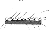
- FIG. 1A shows an LED module 1 (hereinafter also called module) according to an embodiment of the invention.
- the module 1 has at least one light-emitting diode (LED die or LED chip) 2.
- the number of LED chips 2 is not limited by the invention.
- the LED chip 2 preferably has a height of 50 to 500 ⁇ m, preferably 100 to 200 ⁇ m.
- the LED chips 2 are applied to the carrier 3. Amber, red, green and / or blue LED chips 2 (for example RGB) or blue and red LEDs can be used as LED chips 2 for generating monochromatic, white or differently colored, mixed light. Furthermore, the LED chip 2 can be arranged with a photoluminescent material arranged above the LED chip 2, such as, for example, inorganic phosphor (e. G.
- Grenades YAG: Ce 3+ , LuAG: Ce 3+ ; orthosilicates (BOSE): (approx , Sr, Ba) 2 SiO 4 : Eu 2 +, (Ca, Sr) 2 SiO 4 : Eu 2+ , (Sr, Ba) 2 SiO 4 : Eu 2+ , (Ca, Ba) 2 SiO 4 : Eu 2+ ; Nitrides: CaAlSiN 3 : Eu 2+ , (Sr, Ca) AlSiN 3 : Eu 2+ , CaAlSiON 3 : Eu 2+ , ⁇ -SiAlON: Eu 2+ )) and / or organic phosphor (s), can be provided by means of of which the light emitted by the LED chip 2 and the light converted in the photoluminescent material are mixed with one another in such a way that any desired color or white light (for example by means of blue LED and yellow (and / or green and / or red) phosphor ) can be
- the module 1 consists of a carrier 3 and a preferably structured metallic layer 4.
- the carrier 3 is preferably a printed circuit board, the carrier 3 consisting of a metal core, preferably an aluminum plate, and an electrically insulating dielectric and structured copper conductor tracks.
- the metallic layer 4 is applied to the carrier 3; the carrier 3 is preferably coated with the metallic layer 4.
- the metallic layer 4 is preferably a silver layer, a gold layer, an ENIG (Electroless Nickel / Immersion Gold), an ENEPIG (Electroless Nickel / Electroless Palladium / Immersion Gold) or an ENEC / OSP (Electroless Ni / Electroless Cu / OSP (Organic Surface Protection)) and preferably covers the entire surface of the carrier.
- the metallic layer 4 can consist of a surface that can be bonded or at least partially bondable, whereby in the non-bondable surface regions this can additionally be protected against change by oxides or organic layer (s).
- the layer 4 preferably has a thickness of 30 to 8000 nm, particularly preferably a thickness of 100 to 300nm or 2000 to 6000nm. This upper limit is partly technical, but also due to the cost of the silver or gold material as a compromise. According to the invention, thicker / thicker coatings are also conceivable.
- a lacquer layer 5 can be provided, for example, from a highly reflective white paste in such a way that it at least essentially covers the metallic layer 4.
- the lacquer layer 5 is applied to the carrier 3, more precisely the metallic layer 4 of the carrier 3; preferably by means of a dispensing process or a screen printing process.
- the lacquer layer 5 in this embodiment preferably has a thickness or average thickness of 5 to 250 ⁇ m, more preferably 20 to 200 ⁇ m, particularly preferably 100 to 150 ⁇ m.
- the lacquer layer 5 can be realized as a (highly) reflective ceramic white layer or as a white (highly) reflective coating.
- the lacquer layer 5 is preferably a white coating preferably contains pigments made of titanium dioxide (a polymorph of TiO 2, for example TiO 2 (B)), aluminum oxide (Al 2 O 3 ), zirconium dioxide (ZrO 2 ), barium titanate (BaTiO 3 ), silicon dioxide (SiO 2 ), or potassium octatitanate (K 2 Ti 8 O 17 ).
- the pigments preferably consist of a mixture of TiO 2 and / or TiO 2 (B) and / or K 2 Ti 8 O 17 and / or SiO 2 .
- the dispersion further preferably contains an organic (for example ether (s), branched polymeric siloxane (s), preferably methyl and / or hydroxy terminated silsesquioxanes) and / or an inorganic solvent for example.
- an organic for example ether (s), branched polymeric siloxane (s), preferably methyl and / or hydroxy terminated silsesquioxanes
- an inorganic solvent for example. Water.
- the use of a mixture of organic and inorganic solvents is also feasible.
- the at least one LED chip 2 is on the metallic layer 4 (possibly with the previously described one Protective coating) directly applied and electrically contacted (e.g. in a recess of a (FR4) printed circuit board).
- the LED chip 2 can be attached in accordance with a chip-on-board (COB) technology.
- the LED chip 2 can also be applied to the carrier 3 or the lacquer layer 5 (as Figure 1B , 1C ) be. If the LED chip 2 is applied to the metallic layer 4, the lacquer layer 5 is applied only in areas on the metallic layer 4 outside of the LED chip 2.
- the lacquer layer 5 is then preferably applied to the metallic layer 4 before the LED chips 2 are applied to the metallic layer 4.
- the lacquer layer 5 is provided for this purpose in such a way that free spaces 6 remain. In these free spaces 6, the LED chip 2 is applied to the metallic layer 4.
- the distance between the side wall 20 of the LED chip 2 and the lacquer layer 5 is preferably in a range between 50 and 500 ⁇ m, particularly preferably between 100 and 300 ⁇ m.
- the LED chip 2 is preferably glued to the metallic layer 4 by means of an adhesive (not shown).
- the adhesive can be a reflective, preferably white adhesive.
- the adhesive at least partially or completely fills a gap 7 between the side wall 20 of the LED chip 2 and an edge boundary 50 of the ceramic lacquer layer 5 facing the LED chip 2, so that in the latter case the metallic layer 4 completely the lacquer layer 5, the LED chips 2 and the adhesive is covered.
- the adhesive is transparent.
- the module 1 can furthermore have a dam 8 which laterally surrounds the LED chip 2 or the plurality of LED chips 2 and which is at least partially applied to the metallic layer 4 and / or the lacquer layer 5.
- the dam 8 is preferably provided laterally spaced from the LED chip 2.
- a central filling 9 preferably fills the space 80 surrounded by the dam 8.
- the central filling 9 preferably fills the entire volume delimited by the dam 8; the interior 80 formed by the dam 8 is thus preferably filled with the filling 9 up to the highest extent of the dam 8.
- the dam 8 is made higher than the LED chip 2 and consequently projects above it in height, then the top 21 of the LED chip 2 can be covered or coated with the filling material; at least when the volume delimited by the dam 8 is completely filled with the central filling 9.
- the height of the dam 8 is preferably at least two or three times the height of the LED chip 2.
- the dam 8 preferably has a height of 0.1 to 3 mm, particularly preferably 0.25 to 2 mm, most preferably 0.5 up to 1mm.
- the diameter of the cross-sectional area of the dam 8, ie the average thickness of the dam 8 or the maximum distance between the inner wall and the outer wall of the dam 8, corresponds essentially to the height of the dam 8.
- the central filling 9 is preferably made from a matrix material, particularly preferably from a transparent, preferably liquid and temperature-curable polymer or resin or a polymer mixture.
- the central filling 9 preferably has color conversion particles and / or scattering particles 90.
- the material of the dam 8 and the material of the central filling 9 are of the same material class, preferably based on silicone.
- the dam 8 and the central filling 9 can for example be made of a polymer with the same structure. This makes it possible to apply the dam 8 and the filling 9 both in one hardening step, as will be described below.
- the rheological characteristics of the liquid polymer material for building up the wall of the dam 8 must be selected in such a way that the uncured polymer or resin is dimensionally stable until it has cured until it is cured. This approximately solid-like state can be achieved by appropriate admixture of suitable fillers.
- pyrogenic silica silicon dioxide; SiO 2
- other particulate materials fine-grained materials
- At least the inner wall of the dam can be coated with metal or the dam can be made of metal.
- isolation problems may occur with this embodiment.
- the dam 8 alternatively or additionally has (highly) reflective and / or effectively scattering particles with low absorption, such as white pigments.
- white pigments are made, for example, from TiO 2 , BaTiO 3 , BaSO 4 and / or ZrO 2 .
- These reflecting particles are preferably continuously in the mass of the dam 8.
- the dam 8 can contain 10 to 60 percent by weight of the reflecting particles.
- the entire material of the dam 8 will have a non-transparent and preferably white appearance.
- the reflection of light from the LED chip 2 occurs on the inner surface of the dam 8, whereby light is reflected back into the interior of the dam 8 and away from the LED chip 2.
- the dam 8 has the role of a reflector applied in a liquid state on the carrier 3 or the metallic layer 4 or the lacquer layer 5.
- the dam 8 can be applied using dispensing techniques, as described below. However, it is also possible that the dam 8 is a prefabricated element, preferably made of a polymer, ceramic, metal or another plastic. This element can then, for example, be glued in place.
- the dam 8 preferably has the cross-sectional shape of a semicircle, a circle, a rectangle or a square or a polygon.
- the dam 8 In the plan view, that is to say seen perpendicular to the support 3, the dam 8 has a circular, oval, ellipsoidal or angular shape, for example a rectangular or square or polygonal shape.
- the term "dam" is not a limitation on the shape as long as the dam 8 can serve as a dam 8 surrounding the inner central filling 9, and the dam 8 is made of a polymer or resin material , this is already stable in the uncured state.
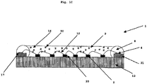
- Figure 1B represents a first illustrative example not belonging to the invention.
- the metal layer 4 only partially covers the carrier 3, the areas under the LED chips 2 and the bond pads 11 (not shown) are preferably covered with the metal layer 4. This results in the areas 10 on the carrier 3 that are not covered by the metal layer 4.
- the lacquer layer 5 covers the metal layer 4 below the LED chips 2, but not the metal layer 4 applied to the bond pads 11.
- the lacquer layer 5 extends down to the carrier surface 17 under the dam 8.
- the lacquer layer 5 preferably completely covers the surface of the carrier 3 under the dam 8. However, the lacquer layer can be applied incompletely to the carrier region under the dam 8.
- the lacquer layer 5 preferably has a thickness or average thickness of 10 to 100 ⁇ m, particularly preferably 20 to 50 ⁇ m.
- the LED chips 2 lie directly on the lacquer layer 5.
- the LED chips 2 are electronically connected to one another with bond wires 12 and to the bond pads 11.
- the ribbon wires 12 are partially mechanically protected by the dam 8 because they are partly below the dam 8.
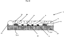
- the carrier 3 with layer 4 can also be used in addition to the examples mentioned 1C (Second illustrative example not belonging to the invention) can be constructed as follows, the structure described below also taken on its own, that is to say without the further features described in the context of the application, in the same or other areas of printed circuit board technology as advantageous (highly) reflective PCB can be used.
- a base material or base substrate 13 for example aluminum plate or gold plate
- This layer preferably has a thickness of 30 to 8000 nm.
- This high-purity aluminum layer can in turn preferably be provided in the manner described above with at least one layer of oxides, which is likewise preferably vapor-deposited.
- the printed circuit board 31 and the layer 4 are partially or preferably completely (as shown) arranged within the dam 8, so that the dam 8 does not (as shown) or only partially covers these components.
- each bond wire 12, and in particular also the one closest to the dam 8 runs completely within the volume delimited to the outside by the dam 8.
- the dam 8 is therefore preferably seated directly and completely on the base substrate 13.
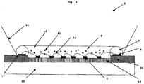
- Base substrate 13 and circuit board 31 form the carrier 3 in the embodiments shown on the 1B-1C and Fig. 4 .
- the printed circuit board 31 and the base substrate 13 can be connected with the aid of an additional substrate 16, for example by an adhesive process or a soldering process (see Fig. 4 ).
- the electrically insulating base or carrier material (usually epoxy resin-impregnated glass fiber mats) of the printed circuit board 31 has a thickness of 30 to 300 ⁇ m, particularly preferably 100 ⁇ m.
- the copper layer (conductor tracks) applied to the carrier material of the (FR4) printed circuit board 31 preferably has a thickness of 18 to 140 ⁇ m, particularly preferably 60 to 90 ⁇ m.
- the finishing surface / metal layer 4 consists of nickel and / or palladium and / or gold (as mentioned earlier, for example ENIG, ENEPIG or ENEC / OSP).
- the metal layer 4 is preferably applied to the surface of the (FR4) printed circuit board 31 (of the carrier 3) under the dam 8.
- the solder mask is preferably white.
- the printed circuit board 31 also preferably has at least one recess 14 (e.g. bore, milling, etc.) in an area in which the LED chip or chips 2 are provided.
- These recess (s) 14 release the underlying aluminum layer or coated aluminum plate (or gold layer) and represent a reflective surface on the (coated) base substrate 13.
- the LED chip 2 can the LED chips 2 are applied directly to the base substrate 13 in the manner described (if appropriate with the above-described protective coating made of oxides).
- a carrier 3 or a printed circuit board can be provided, which enables a high robustness (and thus a certain indestructibility) of the construction.
- the problems associated with the use of silver including the comparatively high cost of silver, are avoided.
- a lacquer layer 5 made from a ceramic lacquer or a ceramic highly reflective white paste can be provided in such a way that it at least partially covers the base substrate 13.
- the lacquer layer 5 can be applied to the base substrate 13; preferably by means of a screen printing process.
- the lacquer layer 5 can also be provided, for example, particularly in the area of a possible recess 14 in a (FR4) printed circuit board and, if appropriate, also cover the base substrate 13 and / or the (FR4) printed circuit board 31 (for example outside of the through a recess 14 in areas of the coated base substrate).
- the lacquer layer 5 preferably has a thickness or average thickness of 10 to 100 ⁇ m, particularly preferably 20 to 50 ⁇ m.
- a reflector 15 can be applied to the circuit board 31 outside the dam (see Fig. 4 ).
- mid- and / or low-power (0.05-0.6 W) LED chips 2 can be mounted inside the dam 8 (in the space 80 surrounding the dam) (for example, see 2A-C ).
- Use of high-power LED chips 2 is also conceivable based on the examples described.
- the LED chips 2 are preferably connected in series (structured in strands 32) (see 2A-C ).
- a strand 32 preferably contains from 5 to 20 LED chips 2, more preferably 10-14 LED chips 2, particularly preferably 12 LED chips 2.
- the LED chips 2 are preferably in 1-15 strands, more preferably in 6- 12 strands on the LED module 1 set up to achieve the shortest electrical connections between LED chips 2 and the bond pads 11.
- the LED module 1 is preferably with from 40 to 160 LED chips 2, particularly preferably from 70 to 150 LED chips 2, for example according to the illustrations 2A-C Equipped evenly and with little space to each other in order to achieve the most homogeneous light distribution possible.
- the LED module 1 can contain 10-50 LED chips 2 set up in 1-4 strands.
- the surface 18 occupied by the LED chips is, for example, from 60% to 90%, preferably 64-75% of the total surface of the room 80.
- the solutions mentioned have the advantage that when using the LED module 1 with an optical element (s) (eg reflector 15, see Fig. 4 ) and / or in a luminaire (e.g. downlight, spotlight, LED bulb, see Fig. 3 ) the homogeneous light distribution / light-emitting surface achieved by the uniform placement of the LED chips 2 is not disadvantageously reshaped.
- an optical element eg reflector 15, see Fig. 4
- a luminaire e.g. downlight, spotlight, LED bulb, see Fig. 3
- the homogeneous light distribution / light-emitting surface achieved by the uniform placement of the LED chips 2 is not disadvantageously reshaped.
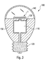
- a spotlight or a retrofit LED lamp 100 can be provided which have at least one LED module 1 according to the invention.
- "Retrofit” lamps are lamps that are designed with regard to their mechanical and electrical connections to replace existing lamps (light bulb, halogen lamp, ). According to its external appearance, it can therefore essentially have the shape of a conventional light bulb or halogen lamp and / or be equipped with a corresponding (lamp) base 120 (for example E27 or E14) or plug (not shown).
- the retrofit LED lamp also usually has its own driver circuit 110 which, for example, adapts the supply current to the operating conditions of the LEDs based on a mains voltage supplied via the base 120.
- the retrofit LED lamps 100 can thus be screwed or inserted into conventional sockets like conventional lamps and operated by means of the supplied mains current.
- the driver circuit 110 can be arranged mechanically and electrically protected in a driver housing 130 as part of a housing.
- the retrofit LED lamp 100 can have a transparent cover 140 as a further part of the housing, which has a glass bulb a conventional light bulb or halogen lamp is simulated.
- heat is generated by the LED module 1 and also by the driver circuit 110. This heat is generally removed (as a further part of the housing) via a heat sink 150 thermally connected to the LED module 1 and the driver circuit 110.
- the LED lamp 100 can also have further electrical, electronic and / or mechanical components, such as, for example, a reflector for the targeted emission of light, a sensor system for measuring and controlling the LED module 1 and other known features of a ballast and / or to emit and / or change the light.
- the geometry of the dam 8 is preferably circular in plan view, other geometries defined by the dam 8 are also possible, such as, for example, rectangular shapes, etc.
- the diameter of the circular dam is preferably from 17 to 28 mm, more preferably from 19 to 26 mm.
- a metallic layer 4 preferably a silver layer (or gold layer) with a thickness of approximately 30 to 8000 nm is applied to a carrier 3 (for example a printed circuit board).
- carrier 3 for example a printed circuit board
- this is provided with a further (protective) layer of oxides.
- Carrier 3 and metallic layer 4 can also consist of a base substrate consisting of aluminum plate with vapor-deposited high-purity aluminum layers and optionally layers of oxides onto which a (FR4) printed circuit board 31 is laminated, which preferably has recesses which the base substrate 13 release at least in places, in which or later on the LED chips 2 can be placed.
- a ceramic lacquer (“ink”) is applied to the carrier 3 - more precisely to the metallic layer 4 of the carrier 3, for example by means of a screen printing process.
- the ceramic lacquer is provided in such a way that the metallic layer 4 of the carrier 3 is at least partially, preferably completely, covered by the lacquer layer 5 formed. It is conceivable that this step is repeated several times (any number of times) in order to increase the layer thickness of the lacquer.
- the lacquer layer 5 has a thickness of approximately 15 to 20 ⁇ m, for example.
- the thickness of the lacquer layer 5 can be increased to a range of, for example, 40 to 50 ⁇ m or more by repeated printing.
- the reflectance of the lacquer layer 5 increases from, for example, 80% at 18 pm to approximately 95% at 40 to 50 ⁇ m. This degree of reflection applies when measuring the paint layer on a black background.
- the light of the LED chip 2 passing through the lacquer layer 5 can be reflected back due to the underlying metallic layer or silver layer 4.
- This double-reflective configuration has the advantage that, for example in the event of an oxidative blackening of the silver layer 4, a substantial proportion of the light is still reflected by the lacquer layer 5 above, which increases the efficiency of the module 1.
- the lacquer layer 5 can also serve as protection against oxidation for the metallic layer 4, so that its reflection properties are essentially retained during the service life of the module 1.
- the lacquer layer 5 applied to the metallic layer 4 is provided according to the invention in such a way that the metallic layer 4 is partially covered by the lacquer layer 5.
- partial means that the metallic layer 4 is not completely covered by the lacquer layer 5, but that free spaces 6 remain, into which the LED chips 2 are later inserted and thus applied to the metallic layer 4.
- the recesses thereof or the locations of the coated base substrate that are thereby exposed preferably at least partially coincide with the clearances 6 into which the LED chips 2 preferably onto the coated base substrate and thus can be applied to the metallic layer 4.
- At least one or more LED chip (s) 2 placed on the metallic layer 4 in the free spaces 6 of the lacquer layer 5; so applied, and electrically contacted.
- the LED chip 2 is preferably attached in accordance with chip-on-board (COB) technology or also as an SMD LED.
- COB chip-on-board
- the bond wires 12 are, for example, in Figure 2A-C shown. However, in configurations outside of the invention, it is also conceivable for the LED chips 2 to be placed on the lacquer layer 5, should the latter cover the entire metallic layer 4.
- the LED chip 2 can also be provided directly on the carrier 3.
- the LED chip 2 is preferably first applied to the carrier 3, so that after the coating it is laterally surrounded by the metallic layer 4 and the lacquer layer 5; the LED chip 2 is then of course not coated in the radiation direction (in particular on its upper side 21).
- the LED chips 2 are preferably glued, particularly preferably glued to the metallic layer 4 or base substrate 13.
- a reflective, preferably white adhesive can advantageously be used.
- the metering of the adhesive should be selected such that when the LED chip 2 is placed on the adhesive, for example in the free spaces 6 of the lacquer layer 5, the latter is laterally displaced such that there is a possibly remaining gap 7 between the side wall 20 of the LED chip 2 and an edge boundary 50 facing the LED chip 2 of the ceramic lacquer layer 5 / the free space 6 (possibly also the metallic layer 4) at least partially or completely, so that the metallic layer 4 (and possibly also the laminated (FR4) circuit board) is completely covered in the latter case.
- a double-reflective configuration can thus also be achieved in areas close to LED chip 2 and over the entire area of module 1 or carrier 3.
- a dam 8 is applied or provided at least partially on the metallic layer 4 (possibly including any laminated (FR4) printed circuit board present) and / or the lacquer layer 5 in such a way that the dam 8 Chips 2 surrounds laterally.
- the dam 8 is preferably formed as an annular dam (for example a torus).
- the dam 8 made of a liquid polymer or resin or a polymer mixture is preferably applied around the LED chips 2 on the metallic layer 4.
- the dam 8 can also at least partially extend over the preferably printed ceramic lacquer layer 5.
- ring or "ring-shaped” in the context of the present description and the claims does not limit the contour of the Walls of the dam 8; e.g. B. the ring does not necessarily have to have a circular shape, but can for example have the shape of a square, an oval, an ellipse or a rectangle etc.
- the circular shape is preferred because of the proximity to circular reflectors, since the plurality of LEDs preferably appear as a single round optical element.
- a square shape is preferred in terms of production technology due to the simpler arrangement.
- a flat plate is preferably used as carrier 3 without depressions, since the reflective effect of walls of a depression can be achieved through the dam walls.
- the cross-sectional shape of the dam 8 can be controlled by the diameter of the dispensing needle used, the flow characteristics of the liquid dam material and the flow (dispensing) speed. Due to the dispensing technology, for example, the cross section of the dam 8 to the summit of the dam 8 can have a tapering shape. As a result, the inner surface of the dam 8 is chamfered and preferably steeper at its upper part, which can be advantageous for reflection purposes.
- the dam 8 can also be produced by means of so-called overmoulding. If this can then no longer be used to protect the wirebonds, the emitting surface increases slightly.
- the dam 8 can also be provided as a prefabricated element, which is preferably made of a polymer or resin, ceramic, metal or another plastic, for example as an injection molded part.
- the space surrounded by the dam 8 is filled with a filling material.
- the volume delimited by the inner walls of the inherently stable ring 8 is filled with a liquid filling material.
- this central filling 9 is preferably made such that the top of the filling 9 is flush with the top of the walls of the dam 8.
- the central filling 9 is particularly preferably provided such that it completely covers or coats the upper side of the LED chip 2.
- the central filling 9 also covers the space between the LED chip 2 and the walls of the dam 8 and touches the lacquer layer 5 and, via free space 6 in the lacquer, the metallic layer (silver layer or high-purity aluminum layer or the like) 4 or the one for applying the LED Chips 2 used glue. Due to the preferred filling with a liquid polymer or resin, the top of the central filling 9 will preferably be flat.
- Liquid unhardened polymer or resin for example silicone
- the materials of the dam 8 and the central filling 9 are preferably similar or the same, so that they are preferably chemically identical.
- the chemical identity should be such that the material used for the dam 8 and the central fill 9 can each be hardened using the same hardening mechanism in order to preferably establish a chemical and / or physical bond between the two materials across their interface .
- the materials of the dam 8 and the central filling 9 can be different; the material of the dam 8, which is preferably identical to the material of the central filling, can also be provided with different 'additives' than the material of the central filling 9.
- the material of the dam 8 which is preferably identical to the material of the central filling, can also be provided with different 'additives' than the material of the central filling 9.
- 9 color conversion particles can be added to the filling material of the central filling for white color conversion LED modules.
- the type and the amount of the color conversion particles depend on the desired color temperature of the LED module 1, which as such are known from the prior art. There is preferably an increasing concentration gradient of the color conversion particles from top to bottom, which z. B. can be achieved by lowering the color conversion particles to the bottom of the filling 9.
- the dam 8 and the central filling 9 are made of a liquid polymer or resin or a polymer mixture, this is preferably hardened after the application or filling.
- the step of applying the dam 8 and filling the dam 8 with the filling material thus preferably further comprises hardening the dam 8, which is preferably made of a liquid polymer / polymer mixture, or hardening the filling material, preferably made of a liquid polymer / polymer mixture, of the central one Filling 9.
- the hardening of the dam 8 and the hardening of the central filling 9 can be carried out after the respective steps for providing the dam 8 and the central filling 9 - that is to say independently of one another.
- This manufacturing process is based on a comparatively high mechanical stability of the material of the wall of the dam 8 in the uncured 'liquid' state.
- additional filling materials such as silicones, can in turn be added to the material of the dam 8.
- the joint hardening of the dam 8 and the central filling 9 consequently has the advantage that polymerization can take place between the dam material and the matrix material of the central filling 9.
- a standardized computer-controlled delivery device can be used both for the manufacture of the dam 8 and for the filling 9.
- the LED chips 2 are first applied to the carrier 3 and then the carrier 3 (except the LED chips 2) is coated with the metallic layer 4 and then the lacquer layer 5 is applied.
- the only decisive factor is that the combination of lacquer layer 5 and metallic layer 4 forms a double reflective effect for the light emitted by the LED chip 2, so that the light of the LED chip 2 passing through the lacquer layer 5 due to the underlying metallic ( Silver) layer 4 reflected back is and thus the efficiency of module 1 is increased.
- the module 1 can also be generally designed, for example, as an electronic or optoelectronic module and have other electronic or optoelectronic components instead of an LED chip.
- module 1 can be designed as a light-erasable memory device, such as an EEPROM.
- the invention can also be used for light-sensitive sensors, such as RGB sensors, infrared sensors or CCD sensors. Infrared emitters and light-sensitive light detection devices are also areas of application, in particular if the sensor is present as a bare chip in the COB or carrier strip technology (lead frame).
- the coating can also be used in connection with light guides and optical fibers.
- An optical fiber, to which light from the light source 2 is to be transmitted, is preferably arranged at a distance from and in front of the light source 2 and extends, for example, out of the filler material 9 away from the light source 2.
- the module 1 can be provided with a mechanical fastening for the optical fibers. Such an arrangement provides improved light transmission from the light source 2 to the optical fiber.
Landscapes
- Engineering & Computer Science (AREA)
- Microelectronics & Electronic Packaging (AREA)
- Led Device Packages (AREA)
Claims (11)
- Module LED (1), comprenant :- un support (3) ayant une réflectivité élevée, une couche métallique (4), de préférence une couche d'argent ou en couche en aluminium extra-pur, étant appliquée sur le support (3),- une couche d'oxyde étant appliquée sur la couche métallique (4), et- une couche de vernis (5) étant prévue sur la couche métallique et la couche d'oxyde,- comprenant en outre une puce LED sur la couche métallique,- la couche de vernis (5) comprenant des zones libres, dans lesquelles les puces LED sont insérées pour être disposées sur la couche métallique (4).
- Module LED selon la revendication 1, dans lequel la couche métallique se compose d'une surface pouvant être liée ou au moins liée par sections, et dans lequel celle-ci est protégée en outre par des couches d'oxydes ou organiques contre toute modification dans les zones de surface ne pouvant pas être liées.
- Module LED selon la revendication 1 ou 2, dans lequel la couche métallique est protégée en outre par des couches organiques ou d'oxydes contre toute modification.
- Module LED selon l'une quelconque des revendications précédentes, lequel est réalisé de telle façon qu'au moins une partie de la lumière incidente sur le module ou générée par la puce LED pouvant être disposée sur le module soit réfléchie par la couche métallique.
- Module LED (1) selon l'une quelconque des revendications précédentes,
dans lequel la couche de vernis (5) est appliquée partiellement sur la couche métallique (4). - Module LED (1) selon l'une quelconque des revendications précédentes, dans lequel la couche de vernis (5) comprend une épaisseur moyenne de 5 à 250 µm, de préférence de 10 à 100 µm, plus préférablement de 20 à 50 µm.
- Module LED (1) selon l'une quelconque des revendications précédentes, dans lequel la couche métallique (4) comprend une épaisseur de 30 nm à 8000 nm, de préférence une épaisseur de 100 nm à 300 nm ou de 2000 nm à 6000 nm.
- Projecteur ou lampe LED de substitution comprenant au moins un module LED (1) selon l'une quelconque des revendications précédentes, de préférence comprenant en outre un ou plusieurs parmi :- un boîtier (130, 140, 150),- un réflecteur (15),- un circuit de pilotage (110),- un système de capteurs,- un dissipateur de chaleur (150) et/ou- un culot de lampe (120).
- Procédé pour la fabrication d'un module LED comprenant un support ayant une réflectivité élevée, le procédé comprenant les étapes suivantes :- application d'une couche métallique (4) sur le support (3),- application d'un vernis céramique sur le support (3) de telle façon que la couche métallique (4) du support (3) soit partiellement recouverte d'une couche de vernis (5) et comprenne des zones libres,- placement d'au moins une puce LED (2) dans les zones libres, de telle sorte que l'au moins une puce LED (2) soit insérée dans les zones libres pour être disposée sur la couche métallique (4).
- Procédé selon la revendication 9, dans lequel le procédé comprend en outre les étapes dans lesquelles plusieurs étapes sont prévues pour l'application du vernis céramique sur la couche métallique (4), de telle sorte que l'épaisseur de couche de la couche de vernis (5) soit accrue.
- Procédé selon l'une quelconque des revendications 9 à 10, dans lequel la puce LED (2) est collée sur la couche métallique (4) dans les zones libres (6) de la couche de vernis (5), de préférence au moyen d'une colle réfléchissante, particulièrement préférablement une colle blanche, et dans lequel le dosage de la colle est choisi de préférence de telle façon que lors du placement de la puce LED (2) sur la colle dans les zones libres (6) la colle est déplacée de telle façon qu'elle remplit l'espace (7) entre la paroi latérale (20) de la puce LED (2) et une des délimitations de bord (50) de la couche de vernis (5) faisant face à la puce LED (2) au moins partiellement ou complètement, de telle sorte que la couche métallique (4) soit complètement recouverte dans le dernier cas cité.
Applications Claiming Priority (5)
| Application Number | Priority Date | Filing Date | Title |
|---|---|---|---|
| DE102012202089 | 2012-02-13 | ||
| ATGM186/2012U AT14124U1 (de) | 2012-02-13 | 2012-04-27 | LED-Modul mit Flächenverguß |
| DE201210223039 DE102012223039A1 (de) | 2012-02-13 | 2012-12-13 | LED-Modul mit Flächenverguß |
| DE202012011948.6U DE202012011948U1 (de) | 2012-02-13 | 2012-12-13 | LED-Modul mit Flächenverguß |
| PCT/EP2013/052435 WO2013120760A1 (fr) | 2012-02-13 | 2013-02-07 | Module de led comprenant un support à haute réflectivité |
Publications (2)
| Publication Number | Publication Date |
|---|---|
| EP2815439A1 EP2815439A1 (fr) | 2014-12-24 |
| EP2815439B1 true EP2815439B1 (fr) | 2020-04-22 |
Family
ID=52780692
Family Applications (1)
| Application Number | Title | Priority Date | Filing Date |
|---|---|---|---|
| EP13705413.6A Not-in-force EP2815439B1 (fr) | 2012-02-13 | 2013-02-07 | Module à DEL avec un substrat de haut reflectivité et procédé de fabrication d'un module à DEL avec un substrat de haut reflectivité |
Country Status (6)
| Country | Link |
|---|---|
| US (1) | US10586901B2 (fr) |
| EP (1) | EP2815439B1 (fr) |
| CN (1) | CN104205378B (fr) |
| AT (1) | AT14124U1 (fr) |
| DE (2) | DE102012223039A1 (fr) |
| WO (1) | WO2013120760A1 (fr) |
Families Citing this family (22)
| Publication number | Priority date | Publication date | Assignee | Title |
|---|---|---|---|---|
| DE102012110774A1 (de) * | 2012-11-09 | 2014-05-15 | Osram Opto Semiconductors Gmbh | Optoelektronisches Halbleiterbauteil |
| JP6249348B2 (ja) * | 2013-11-22 | 2017-12-20 | 東芝ライテック株式会社 | 発光装置 |
| CN104835809A (zh) * | 2014-02-10 | 2015-08-12 | 漳州灿坤实业有限公司 | 一种led发光装置 |
| US10453825B2 (en) * | 2014-11-11 | 2019-10-22 | Cree, Inc. | Light emitting diode (LED) components and methods |
| DE102015112969A1 (de) * | 2015-08-06 | 2017-02-09 | Osram Opto Semiconductors Gmbh | Verfahren zum Herstellen eines optoelektronischen Bauelements |
| CN105623658B (zh) * | 2016-01-29 | 2017-04-12 | 江苏博睿光电有限公司 | 一种氮氧化物荧光粉及其制备方法、氮氧化物发光体和发光器件 |
| DE102016202801A1 (de) * | 2016-02-24 | 2017-08-24 | Tridonic Jennersdorf Gmbh | LED-Modul mit Isolierdamm |
| DE102016103819A1 (de) * | 2016-03-03 | 2017-09-07 | Heraeus Deutschland GmbH & Co. KG | Anschlussträger, optoelektronisches Bauteil und Verfahren zur Herstellung eines Anschlussträgers oder eines optoelektronischen Bauteils |
| EP3451394B1 (fr) * | 2016-04-26 | 2021-01-06 | Citizen Electronics Co., Ltd. | Dispositif électroluminescent |
| JP6683000B2 (ja) * | 2016-05-09 | 2020-04-15 | 日亜化学工業株式会社 | 発光装置及びその製造方法 |
| CN110612611B (zh) * | 2016-05-24 | 2022-10-11 | 西铁城电子株式会社 | Led照明装置及led照明装置的制造方法 |
| DE102016112293A1 (de) * | 2016-07-05 | 2018-01-11 | Osram Opto Semiconductors Gmbh | Verfahren zum herstellen eines optoelektronischen bauelements und optoelektronisches bauelement |
| DE102016116298A1 (de) * | 2016-09-01 | 2018-03-01 | Osram Opto Semiconductors Gmbh | Anordnung mit Träger und optoelektronischem Bauelement |
| DE102016219116A1 (de) * | 2016-09-30 | 2018-04-05 | Robert Bosch Gmbh | Verfahren zum Herstellen einer elektronischen Baugruppe und elektronische Baugruppe, insbesondere für ein Getriebesteuermodul |
| JP7177327B2 (ja) * | 2017-04-06 | 2022-11-24 | 日亜化学工業株式会社 | 発光装置 |
| US10957736B2 (en) | 2018-03-12 | 2021-03-23 | Cree, Inc. | Light emitting diode (LED) components and methods |
| KR102613239B1 (ko) | 2018-06-04 | 2023-12-14 | 삼성전자주식회사 | 백색 led 모듈 및 조명 장치 |
| JP6923808B2 (ja) * | 2018-06-22 | 2021-08-25 | 日亜化学工業株式会社 | 発光装置及びその製造方法 |
| US11189764B2 (en) | 2018-11-22 | 2021-11-30 | Nichia Corporation | Light-emitting device and manufacturing method thereof |
| CN110701515A (zh) * | 2019-10-12 | 2020-01-17 | 安徽连达光电科技有限公司 | 一种带有透镜的低成本节能灯的led吸顶灯模组及生产工艺 |
| WO2021117400A1 (fr) * | 2019-12-11 | 2021-06-17 | ヌヴォトンテクノロジージャパン株式会社 | Dispositif à semi-conducteur |
| CN115201946A (zh) * | 2022-07-27 | 2022-10-18 | 深圳同兴达科技股份有限公司 | 一种mini LED灯板围坝散光结构及其制作方法 |
Family Cites Families (34)
| Publication number | Priority date | Publication date | Assignee | Title |
|---|---|---|---|---|
| DE10024336A1 (de) * | 2000-05-17 | 2001-11-22 | Heidenhain Gmbh Dr Johannes | Bauelementanordnung und Verfahren zur Herstellung einer Bauelementanordnung |
| JP2003051620A (ja) * | 2001-08-08 | 2003-02-21 | Rohm Co Ltd | 半導体発光装置 |
| DE10245946C1 (de) * | 2002-09-30 | 2003-10-23 | Osram Opto Semiconductors Gmbh | Verfahren zur Herstellung eines Lichtquellenmoduls |
| US7095053B2 (en) * | 2003-05-05 | 2006-08-22 | Lamina Ceramics, Inc. | Light emitting diodes packaged for high temperature operation |
| US20100002455A1 (en) * | 2005-11-24 | 2010-01-07 | Yoichi Matsuoka | Electronic Component Mounting Board and Method for Manufacturing Such Board |
| TW200802957A (en) * | 2006-06-16 | 2008-01-01 | Gigno Technology Co Ltd | Light emitting diode module |
| EP1914809A1 (fr) * | 2006-10-20 | 2008-04-23 | Tridonic Optoelectronics GmbH | Housse pour des composants optoéléctroniques |
| KR101555386B1 (ko) * | 2007-05-18 | 2015-09-23 | 덴끼 가가꾸 고교 가부시키가이샤 | 금속 베이스 회로 기판 |
| TW200905905A (en) * | 2007-07-18 | 2009-02-01 | Lee Ko Hsin | Method of manufacture of light emitting diode |
| JP5345363B2 (ja) * | 2008-06-24 | 2013-11-20 | シャープ株式会社 | 発光装置 |
| JP2010199547A (ja) * | 2009-01-30 | 2010-09-09 | Nichia Corp | 発光装置及びその製造方法 |
| US20100193825A1 (en) * | 2009-02-05 | 2010-08-05 | Chih-Wen Yang | Light-emitting diode package and method for fabricating the same |
| CN102369607A (zh) * | 2009-03-31 | 2012-03-07 | 东芝照明技术株式会社 | 发光装置及照明装置 |
| JP5499325B2 (ja) * | 2009-06-01 | 2014-05-21 | 東芝ライテック株式会社 | 発光モジュールおよび照明装置 |
| JP5726409B2 (ja) * | 2009-07-01 | 2015-06-03 | シャープ株式会社 | 発光装置および発光装置の製造方法 |
| US9048404B2 (en) | 2009-07-06 | 2015-06-02 | Zhuo Sun | Thin flat solid state light source module |
| WO2011007874A1 (fr) * | 2009-07-17 | 2011-01-20 | 電気化学工業株式会社 | Ensemble puce à del, boîtier de del et procédé de fabrication de boîtier de del |
| US20110121326A1 (en) * | 2009-11-26 | 2011-05-26 | Dsem Holdings Sdn. Bhd. | Submount Having Reflective Cu-Ni-Ag Pads Formed Using Electroless Deposition |
| JP2011151268A (ja) * | 2010-01-22 | 2011-08-04 | Sharp Corp | 発光装置 |
| JP2011151248A (ja) * | 2010-01-22 | 2011-08-04 | Seiwa Electric Mfg Co Ltd | 発光装置及び発光装置の製造方法 |
| JPWO2011092945A1 (ja) * | 2010-01-28 | 2013-05-30 | 旭硝子株式会社 | 発光素子搭載用基板、その製造方法および発光装置 |
| US20110186874A1 (en) * | 2010-02-03 | 2011-08-04 | Soraa, Inc. | White Light Apparatus and Method |
| DE202010017532U1 (de) * | 2010-03-16 | 2012-01-19 | Eppsteinfoils Gmbh & Co.Kg | Foliensystem für LED-Anwendungen |
| US20130009190A1 (en) * | 2010-04-07 | 2013-01-10 | Yuhichi Memida | Light emitting device and method for manufacturing same |
| US9012938B2 (en) | 2010-04-09 | 2015-04-21 | Cree, Inc. | High reflective substrate of light emitting devices with improved light output |
| DE102010027748A1 (de) * | 2010-04-14 | 2011-10-20 | Osram Opto Semiconductors Gmbh | Optoelektronisches Bauelement |
| EP2378576A2 (fr) * | 2010-04-15 | 2011-10-19 | Samsung LED Co., Ltd. | Boîtier avec diode électroluminescente, appareil d'éclairage l'incorporant, et procédé de fabrication dudit boîtier |
| JP2012033853A (ja) * | 2010-04-28 | 2012-02-16 | Fujifilm Corp | 絶縁性光反射基板 |
| TWI472067B (zh) * | 2010-04-28 | 2015-02-01 | Lg伊諾特股份有限公司 | 光學封裝及其製造方法 |
| JP5429038B2 (ja) * | 2010-05-14 | 2014-02-26 | 旭硝子株式会社 | 発光素子搭載用基板および発光装置 |
| JP2012015330A (ja) * | 2010-06-30 | 2012-01-19 | Toshiba Lighting & Technology Corp | 発光モジュールおよび照明装置 |
| JP2012033855A (ja) | 2010-07-01 | 2012-02-16 | Hitachi Cable Ltd | Ledモジュール、ledパッケージ、並びに配線基板およびその製造方法 |
| JP5486431B2 (ja) * | 2010-07-27 | 2014-05-07 | 日東電工株式会社 | 発光装置用部品、発光装置およびその製造方法 |
| US9461023B2 (en) * | 2011-10-28 | 2016-10-04 | Bridgelux, Inc. | Jetting a highly reflective layer onto an LED assembly |
-
2012
- 2012-04-27 AT ATGM186/2012U patent/AT14124U1/de not_active IP Right Cessation
- 2012-12-13 DE DE201210223039 patent/DE102012223039A1/de not_active Ceased
- 2012-12-13 DE DE202012011948.6U patent/DE202012011948U1/de not_active Expired - Lifetime
-
2013
- 2013-02-07 WO PCT/EP2013/052435 patent/WO2013120760A1/fr not_active Ceased
- 2013-02-07 CN CN201380018764.7A patent/CN104205378B/zh not_active Expired - Fee Related
- 2013-02-07 EP EP13705413.6A patent/EP2815439B1/fr not_active Not-in-force
- 2013-02-07 US US14/378,581 patent/US10586901B2/en active Active
Non-Patent Citations (1)
| Title |
|---|
| None * |
Also Published As
| Publication number | Publication date |
|---|---|
| DE102012223039A1 (de) | 2013-08-14 |
| AT14124U1 (de) | 2015-04-15 |
| DE202012011948U1 (de) | 2014-03-20 |
| EP2815439A1 (fr) | 2014-12-24 |
| US10586901B2 (en) | 2020-03-10 |
| US20150016107A1 (en) | 2015-01-15 |
| CN104205378B (zh) | 2018-02-02 |
| WO2013120760A1 (fr) | 2013-08-22 |
| CN104205378A (zh) | 2014-12-10 |
Similar Documents
| Publication | Publication Date | Title |
|---|---|---|
| EP2815439B1 (fr) | Module à DEL avec un substrat de haut reflectivité et procédé de fabrication d'un module à DEL avec un substrat de haut reflectivité | |
| DE69838597T2 (de) | Lichtemittierende Halbleitervorrichtung und Herstellungsverfahren | |
| DE112019001502B4 (de) | Optoelektronisches bauelement und verfahren zur herstellung eines optoelektronischen bauelements | |
| DE202008018207U1 (de) | Baugruppe mit lichtemittierender Vorrichtung | |
| EP2845233B1 (fr) | Module de del | |
| EP2382673A1 (fr) | Composant semi-conducteur optoélectronique | |
| DE202009018419U1 (de) | LED-Modul mit verbesserter Lichtleistung | |
| WO2016034540A1 (fr) | Composant à diode électroluminescente | |
| DE112007000773T5 (de) | Licht emittierende Vorrichtung | |
| DE102017104606A1 (de) | Lichtemittierender Apparat und Beleuchtungsapparat | |
| DE102010016720B4 (de) | Leuchtdiodenanordnung für hohe Sicherheitsanforderungen | |
| DE102015113640A1 (de) | Licht emittierende Vorrichtung und Leuchtvorrichtung | |
| DE112013000768B4 (de) | Leuchtdiodeneinheit | |
| DE102014109717A1 (de) | Substrat, Licht emittierende Vorrichtung, Beleuchtungslichtquelle und Leuchteinrichtung | |
| WO2014207037A1 (fr) | Composant optoélectronique et procédé pour le fabriquer | |
| DE102013207579B4 (de) | LED-Modul mit hoher Lichtstromdichte | |
| WO2013110540A1 (fr) | Lampe et procédé de fabrication d'une lampe | |
| DE102010061801A1 (de) | LED-Modul mit gemeinsamem Farbumwandlungsmodul für wenigstens zwei LED-Chips | |
| EP2626918B1 (fr) | Module à DEL avec un substrat de haute reflectivité et procédé de fabrication d'un module à DEL avec un substrat de haute reflectivité | |
| WO2017001327A1 (fr) | Dispositif d'éclairage optoélectronique | |
| EP3229269B1 (fr) | Module del selon une technologie chip on board | |
| DE102016114175A1 (de) | Licht emittierende Einrichtung und Beleuchtungseinrichtung | |
| EP3424081B1 (fr) | Module de led csp à émission de lumière améliorée | |
| DE102014205470B4 (de) | Leuchtvorrichtung mit CoB-Bereich | |
| DE102012006924A1 (de) | LED-Beleuchtungsmodul mit gleichförmiger Lichtabgabe |
Legal Events
| Date | Code | Title | Description |
|---|---|---|---|
| PUAI | Public reference made under article 153(3) epc to a published international application that has entered the european phase |
Free format text: ORIGINAL CODE: 0009012 |
|
| 17P | Request for examination filed |
Effective date: 20140904 |
|
| AK | Designated contracting states |
Kind code of ref document: A1 Designated state(s): AL AT BE BG CH CY CZ DE DK EE ES FI FR GB GR HR HU IE IS IT LI LT LU LV MC MK MT NL NO PL PT RO RS SE SI SK SM TR |
|
| AX | Request for extension of the european patent |
Extension state: BA ME |
|
| DAX | Request for extension of the european patent (deleted) | ||
| STAA | Information on the status of an ep patent application or granted ep patent |
Free format text: STATUS: EXAMINATION IS IN PROGRESS |
|
| 17Q | First examination report despatched |
Effective date: 20190129 |
|
| RIC1 | Information provided on ipc code assigned before grant |
Ipc: H01L 33/60 20100101AFI20191202BHEP Ipc: H01L 33/64 20100101ALI20191202BHEP Ipc: H05K 1/02 20060101ALN20191202BHEP Ipc: H01L 23/00 20060101ALN20191202BHEP |
|
| GRAP | Despatch of communication of intention to grant a patent |
Free format text: ORIGINAL CODE: EPIDOSNIGR1 |
|
| STAA | Information on the status of an ep patent application or granted ep patent |
Free format text: STATUS: GRANT OF PATENT IS INTENDED |
|
| INTG | Intention to grant announced |
Effective date: 20200110 |
|
| GRAS | Grant fee paid |
Free format text: ORIGINAL CODE: EPIDOSNIGR3 |
|
| GRAA | (expected) grant |
Free format text: ORIGINAL CODE: 0009210 |
|
| STAA | Information on the status of an ep patent application or granted ep patent |
Free format text: STATUS: THE PATENT HAS BEEN GRANTED |
|
| RAP1 | Party data changed (applicant data changed or rights of an application transferred) |
Owner name: TRIDONIC GMBH & CO. KG |
|
| AK | Designated contracting states |
Kind code of ref document: B1 Designated state(s): AL AT BE BG CH CY CZ DE DK EE ES FI FR GB GR HR HU IE IS IT LI LT LU LV MC MK MT NL NO PL PT RO RS SE SI SK SM TR |
|
| REG | Reference to a national code |
Ref country code: GB Ref legal event code: FG4D Free format text: NOT ENGLISH |
|
| REG | Reference to a national code |
Ref country code: CH Ref legal event code: EP |
|
| REG | Reference to a national code |
Ref country code: IE Ref legal event code: FG4D Free format text: LANGUAGE OF EP DOCUMENT: GERMAN |
|
| REG | Reference to a national code |
Ref country code: DE Ref legal event code: R096 Ref document number: 502013014615 Country of ref document: DE |
|
| REG | Reference to a national code |
Ref country code: AT Ref legal event code: REF Ref document number: 1261301 Country of ref document: AT Kind code of ref document: T Effective date: 20200515 |
|
| REG | Reference to a national code |
Ref country code: LT Ref legal event code: MG4D |
|
| REG | Reference to a national code |
Ref country code: NL Ref legal event code: MP Effective date: 20200422 |
|
| PG25 | Lapsed in a contracting state [announced via postgrant information from national office to epo] |
Ref country code: SE Free format text: LAPSE BECAUSE OF FAILURE TO SUBMIT A TRANSLATION OF THE DESCRIPTION OR TO PAY THE FEE WITHIN THE PRESCRIBED TIME-LIMIT Effective date: 20200422 Ref country code: NO Free format text: LAPSE BECAUSE OF FAILURE TO SUBMIT A TRANSLATION OF THE DESCRIPTION OR TO PAY THE FEE WITHIN THE PRESCRIBED TIME-LIMIT Effective date: 20200722 Ref country code: FI Free format text: LAPSE BECAUSE OF FAILURE TO SUBMIT A TRANSLATION OF THE DESCRIPTION OR TO PAY THE FEE WITHIN THE PRESCRIBED TIME-LIMIT Effective date: 20200422 Ref country code: GR Free format text: LAPSE BECAUSE OF FAILURE TO SUBMIT A TRANSLATION OF THE DESCRIPTION OR TO PAY THE FEE WITHIN THE PRESCRIBED TIME-LIMIT Effective date: 20200723 Ref country code: IS Free format text: LAPSE BECAUSE OF FAILURE TO SUBMIT A TRANSLATION OF THE DESCRIPTION OR TO PAY THE FEE WITHIN THE PRESCRIBED TIME-LIMIT Effective date: 20200822 Ref country code: PT Free format text: LAPSE BECAUSE OF FAILURE TO SUBMIT A TRANSLATION OF THE DESCRIPTION OR TO PAY THE FEE WITHIN THE PRESCRIBED TIME-LIMIT Effective date: 20200824 Ref country code: LT Free format text: LAPSE BECAUSE OF FAILURE TO SUBMIT A TRANSLATION OF THE DESCRIPTION OR TO PAY THE FEE WITHIN THE PRESCRIBED TIME-LIMIT Effective date: 20200422 Ref country code: NL Free format text: LAPSE BECAUSE OF FAILURE TO SUBMIT A TRANSLATION OF THE DESCRIPTION OR TO PAY THE FEE WITHIN THE PRESCRIBED TIME-LIMIT Effective date: 20200422 |
|
| PG25 | Lapsed in a contracting state [announced via postgrant information from national office to epo] |
Ref country code: LV Free format text: LAPSE BECAUSE OF FAILURE TO SUBMIT A TRANSLATION OF THE DESCRIPTION OR TO PAY THE FEE WITHIN THE PRESCRIBED TIME-LIMIT Effective date: 20200422 Ref country code: HR Free format text: LAPSE BECAUSE OF FAILURE TO SUBMIT A TRANSLATION OF THE DESCRIPTION OR TO PAY THE FEE WITHIN THE PRESCRIBED TIME-LIMIT Effective date: 20200422 Ref country code: BG Free format text: LAPSE BECAUSE OF FAILURE TO SUBMIT A TRANSLATION OF THE DESCRIPTION OR TO PAY THE FEE WITHIN THE PRESCRIBED TIME-LIMIT Effective date: 20200722 Ref country code: RS Free format text: LAPSE BECAUSE OF FAILURE TO SUBMIT A TRANSLATION OF THE DESCRIPTION OR TO PAY THE FEE WITHIN THE PRESCRIBED TIME-LIMIT Effective date: 20200422 |
|
| PG25 | Lapsed in a contracting state [announced via postgrant information from national office to epo] |
Ref country code: AL Free format text: LAPSE BECAUSE OF FAILURE TO SUBMIT A TRANSLATION OF THE DESCRIPTION OR TO PAY THE FEE WITHIN THE PRESCRIBED TIME-LIMIT Effective date: 20200422 |
|
| REG | Reference to a national code |
Ref country code: DE Ref legal event code: R097 Ref document number: 502013014615 Country of ref document: DE |
|
| PG25 | Lapsed in a contracting state [announced via postgrant information from national office to epo] |
Ref country code: SM Free format text: LAPSE BECAUSE OF FAILURE TO SUBMIT A TRANSLATION OF THE DESCRIPTION OR TO PAY THE FEE WITHIN THE PRESCRIBED TIME-LIMIT Effective date: 20200422 Ref country code: EE Free format text: LAPSE BECAUSE OF FAILURE TO SUBMIT A TRANSLATION OF THE DESCRIPTION OR TO PAY THE FEE WITHIN THE PRESCRIBED TIME-LIMIT Effective date: 20200422 Ref country code: DK Free format text: LAPSE BECAUSE OF FAILURE TO SUBMIT A TRANSLATION OF THE DESCRIPTION OR TO PAY THE FEE WITHIN THE PRESCRIBED TIME-LIMIT Effective date: 20200422 Ref country code: RO Free format text: LAPSE BECAUSE OF FAILURE TO SUBMIT A TRANSLATION OF THE DESCRIPTION OR TO PAY THE FEE WITHIN THE PRESCRIBED TIME-LIMIT Effective date: 20200422 Ref country code: CZ Free format text: LAPSE BECAUSE OF FAILURE TO SUBMIT A TRANSLATION OF THE DESCRIPTION OR TO PAY THE FEE WITHIN THE PRESCRIBED TIME-LIMIT Effective date: 20200422 Ref country code: ES Free format text: LAPSE BECAUSE OF FAILURE TO SUBMIT A TRANSLATION OF THE DESCRIPTION OR TO PAY THE FEE WITHIN THE PRESCRIBED TIME-LIMIT Effective date: 20200422 Ref country code: IT Free format text: LAPSE BECAUSE OF FAILURE TO SUBMIT A TRANSLATION OF THE DESCRIPTION OR TO PAY THE FEE WITHIN THE PRESCRIBED TIME-LIMIT Effective date: 20200422 |
|
| REG | Reference to a national code |
Ref country code: DE Ref legal event code: R084 Ref document number: 502013014615 Country of ref document: DE |
|
| PG25 | Lapsed in a contracting state [announced via postgrant information from national office to epo] |
Ref country code: PL Free format text: LAPSE BECAUSE OF FAILURE TO SUBMIT A TRANSLATION OF THE DESCRIPTION OR TO PAY THE FEE WITHIN THE PRESCRIBED TIME-LIMIT Effective date: 20200422 Ref country code: SK Free format text: LAPSE BECAUSE OF FAILURE TO SUBMIT A TRANSLATION OF THE DESCRIPTION OR TO PAY THE FEE WITHIN THE PRESCRIBED TIME-LIMIT Effective date: 20200422 |
|
| PLBE | No opposition filed within time limit |
Free format text: ORIGINAL CODE: 0009261 |
|
| STAA | Information on the status of an ep patent application or granted ep patent |
Free format text: STATUS: NO OPPOSITION FILED WITHIN TIME LIMIT |
|
| 26N | No opposition filed |
Effective date: 20210125 |
|
| PG25 | Lapsed in a contracting state [announced via postgrant information from national office to epo] |
Ref country code: SI Free format text: LAPSE BECAUSE OF FAILURE TO SUBMIT A TRANSLATION OF THE DESCRIPTION OR TO PAY THE FEE WITHIN THE PRESCRIBED TIME-LIMIT Effective date: 20200422 |
|
| PG25 | Lapsed in a contracting state [announced via postgrant information from national office to epo] |
Ref country code: MC Free format text: LAPSE BECAUSE OF FAILURE TO SUBMIT A TRANSLATION OF THE DESCRIPTION OR TO PAY THE FEE WITHIN THE PRESCRIBED TIME-LIMIT Effective date: 20200422 |
|
| REG | Reference to a national code |
Ref country code: BE Ref legal event code: MM Effective date: 20210228 |
|
| PG25 | Lapsed in a contracting state [announced via postgrant information from national office to epo] |
Ref country code: LI Free format text: LAPSE BECAUSE OF NON-PAYMENT OF DUE FEES Effective date: 20210228 Ref country code: LU Free format text: LAPSE BECAUSE OF NON-PAYMENT OF DUE FEES Effective date: 20210207 Ref country code: CH Free format text: LAPSE BECAUSE OF NON-PAYMENT OF DUE FEES Effective date: 20210228 |
|
| PG25 | Lapsed in a contracting state [announced via postgrant information from national office to epo] |
Ref country code: IE Free format text: LAPSE BECAUSE OF NON-PAYMENT OF DUE FEES Effective date: 20210207 |
|
| REG | Reference to a national code |
Ref country code: AT Ref legal event code: MM01 Ref document number: 1261301 Country of ref document: AT Kind code of ref document: T Effective date: 20210207 |
|
| PG25 | Lapsed in a contracting state [announced via postgrant information from national office to epo] |
Ref country code: AT Free format text: LAPSE BECAUSE OF NON-PAYMENT OF DUE FEES Effective date: 20210207 |
|
| PGFP | Annual fee paid to national office [announced via postgrant information from national office to epo] |
Ref country code: GB Payment date: 20220222 Year of fee payment: 10 |
|
| PGFP | Annual fee paid to national office [announced via postgrant information from national office to epo] |
Ref country code: FR Payment date: 20220224 Year of fee payment: 10 |
|
| PG25 | Lapsed in a contracting state [announced via postgrant information from national office to epo] |
Ref country code: BE Free format text: LAPSE BECAUSE OF NON-PAYMENT OF DUE FEES Effective date: 20210228 |
|
| PG25 | Lapsed in a contracting state [announced via postgrant information from national office to epo] |
Ref country code: HU Free format text: LAPSE BECAUSE OF FAILURE TO SUBMIT A TRANSLATION OF THE DESCRIPTION OR TO PAY THE FEE WITHIN THE PRESCRIBED TIME-LIMIT; INVALID AB INITIO Effective date: 20130207 |
|
| PGFP | Annual fee paid to national office [announced via postgrant information from national office to epo] |
Ref country code: DE Payment date: 20230227 Year of fee payment: 11 |
|
| PG25 | Lapsed in a contracting state [announced via postgrant information from national office to epo] |
Ref country code: CY Free format text: LAPSE BECAUSE OF FAILURE TO SUBMIT A TRANSLATION OF THE DESCRIPTION OR TO PAY THE FEE WITHIN THE PRESCRIBED TIME-LIMIT Effective date: 20200422 |
|
| P01 | Opt-out of the competence of the unified patent court (upc) registered |
Effective date: 20230530 |
|
| GBPC | Gb: european patent ceased through non-payment of renewal fee |
Effective date: 20230207 |
|
| PG25 | Lapsed in a contracting state [announced via postgrant information from national office to epo] |
Ref country code: GB Free format text: LAPSE BECAUSE OF NON-PAYMENT OF DUE FEES Effective date: 20230207 |
|
| PG25 | Lapsed in a contracting state [announced via postgrant information from national office to epo] |
Ref country code: GB Free format text: LAPSE BECAUSE OF NON-PAYMENT OF DUE FEES Effective date: 20230207 Ref country code: FR Free format text: LAPSE BECAUSE OF NON-PAYMENT OF DUE FEES Effective date: 20230228 |
|
| PG25 | Lapsed in a contracting state [announced via postgrant information from national office to epo] |
Ref country code: MK Free format text: LAPSE BECAUSE OF FAILURE TO SUBMIT A TRANSLATION OF THE DESCRIPTION OR TO PAY THE FEE WITHIN THE PRESCRIBED TIME-LIMIT Effective date: 20200422 |
|
| REG | Reference to a national code |
Ref country code: DE Ref legal event code: R119 Ref document number: 502013014615 Country of ref document: DE |
|
| PG25 | Lapsed in a contracting state [announced via postgrant information from national office to epo] |
Ref country code: MT Free format text: LAPSE BECAUSE OF FAILURE TO SUBMIT A TRANSLATION OF THE DESCRIPTION OR TO PAY THE FEE WITHIN THE PRESCRIBED TIME-LIMIT Effective date: 20200422 |
|
| PG25 | Lapsed in a contracting state [announced via postgrant information from national office to epo] |
Ref country code: DE Free format text: LAPSE BECAUSE OF NON-PAYMENT OF DUE FEES Effective date: 20240903 |
|
| PG25 | Lapsed in a contracting state [announced via postgrant information from national office to epo] |
Ref country code: DE Free format text: LAPSE BECAUSE OF NON-PAYMENT OF DUE FEES Effective date: 20240903 |
|
| PG25 | Lapsed in a contracting state [announced via postgrant information from national office to epo] |
Ref country code: TR Free format text: LAPSE BECAUSE OF FAILURE TO SUBMIT A TRANSLATION OF THE DESCRIPTION OR TO PAY THE FEE WITHIN THE PRESCRIBED TIME-LIMIT Effective date: 20200422 |