EP2819492B1 - Composant MID, procédé de fabrication - Google Patents
Composant MID, procédé de fabrication Download PDFInfo
- Publication number
- EP2819492B1 EP2819492B1 EP14171870.0A EP14171870A EP2819492B1 EP 2819492 B1 EP2819492 B1 EP 2819492B1 EP 14171870 A EP14171870 A EP 14171870A EP 2819492 B1 EP2819492 B1 EP 2819492B1
- Authority
- EP
- European Patent Office
- Prior art keywords
- interposer
- component
- plastic
- plastic encapsulation
- mid
- Prior art date
- Legal status (The legal status is an assumption and is not a legal conclusion. Google has not performed a legal analysis and makes no representation as to the accuracy of the status listed.)
- Active
Links
Images

Classifications
-
- H—ELECTRICITY
- H05—ELECTRIC TECHNIQUES NOT OTHERWISE PROVIDED FOR
- H05K—PRINTED CIRCUITS; CASINGS OR CONSTRUCTIONAL DETAILS OF ELECTRIC APPARATUS; MANUFACTURE OF ASSEMBLAGES OF ELECTRICAL COMPONENTS
- H05K3/00—Apparatus or processes for manufacturing printed circuits
- H05K3/22—Secondary treatment of printed circuits
- H05K3/28—Applying non-metallic protective coatings
- H05K3/284—Applying non-metallic protective coatings for encapsulating mounted components
-
- H—ELECTRICITY
- H05—ELECTRIC TECHNIQUES NOT OTHERWISE PROVIDED FOR
- H05K—PRINTED CIRCUITS; CASINGS OR CONSTRUCTIONAL DETAILS OF ELECTRIC APPARATUS; MANUFACTURE OF ASSEMBLAGES OF ELECTRICAL COMPONENTS
- H05K1/00—Printed circuits
- H05K1/18—Printed circuits structurally associated with non-printed electric components
- H05K1/189—Printed circuits structurally associated with non-printed electric components characterised by the use of flexible or folded printed circuits
-
- H—ELECTRICITY
- H05—ELECTRIC TECHNIQUES NOT OTHERWISE PROVIDED FOR
- H05K—PRINTED CIRCUITS; CASINGS OR CONSTRUCTIONAL DETAILS OF ELECTRIC APPARATUS; MANUFACTURE OF ASSEMBLAGES OF ELECTRICAL COMPONENTS
- H05K2201/00—Indexing scheme relating to printed circuits covered by H05K1/00
- H05K2201/10—Details of components or other objects attached to or integrated in a printed circuit board
- H05K2201/10007—Types of components
- H05K2201/10151—Sensor
-
- H—ELECTRICITY
- H05—ELECTRIC TECHNIQUES NOT OTHERWISE PROVIDED FOR
- H05K—PRINTED CIRCUITS; CASINGS OR CONSTRUCTIONAL DETAILS OF ELECTRIC APPARATUS; MANUFACTURE OF ASSEMBLAGES OF ELECTRICAL COMPONENTS
- H05K2203/00—Indexing scheme relating to apparatus or processes for manufacturing printed circuits covered by H05K3/00
- H05K2203/13—Moulding and encapsulation; Deposition techniques; Protective layers
- H05K2203/1305—Moulding and encapsulation
- H05K2203/1316—Moulded encapsulation of mounted components
-
- H—ELECTRICITY
- H05—ELECTRIC TECHNIQUES NOT OTHERWISE PROVIDED FOR
- H05K—PRINTED CIRCUITS; CASINGS OR CONSTRUCTIONAL DETAILS OF ELECTRIC APPARATUS; MANUFACTURE OF ASSEMBLAGES OF ELECTRICAL COMPONENTS
- H05K2203/00—Indexing scheme relating to apparatus or processes for manufacturing printed circuits covered by H05K3/00
- H05K2203/13—Moulding and encapsulation; Deposition techniques; Protective layers
- H05K2203/1305—Moulding and encapsulation
- H05K2203/1327—Moulding over PCB locally or completely
-
- H—ELECTRICITY
- H10—SEMICONDUCTOR DEVICES; ELECTRIC SOLID-STATE DEVICES NOT OTHERWISE PROVIDED FOR
- H10W—GENERIC PACKAGES, INTERCONNECTIONS, CONNECTORS OR OTHER CONSTRUCTIONAL DETAILS OF DEVICES COVERED BY CLASS H10
- H10W90/00—Package configurations
- H10W90/701—Package configurations characterised by the relative positions of pads or connectors relative to package parts
- H10W90/721—Package configurations characterised by the relative positions of pads or connectors relative to package parts of bump connectors
- H10W90/724—Package configurations characterised by the relative positions of pads or connectors relative to package parts of bump connectors between a chip and a stacked insulating package substrate, interposer or RDL
Definitions
- the invention relates to an MID component for a control device or a sensor, in particular of a vehicle, with a circuit carrier and with a plastic encapsulation, which einhaust the circuit substrate at least partially.
- the invention relates to a method for producing such a MID component.
- MID components and methods for their preparation of the type mentioned are known from the prior art.
- an electronic component is usually referred to, in which at least one metallic conductor track is arranged on a plastic carrier. Due to their robustness and their compact design, MID components are frequently used in the automotive industry.
- MID components are manufactured in three-dimensional design using different technologies. For example, the DE 10 2010 041 121 A1 a circuit carrier with a lead frame (punched grid), which is inserted into an injection mold and molded with plastic, so that the conductor tracks run within the plastic. By applying further conductor tracks on the outside of the plastic part, multi-layer conductor track structures can thus be realized.
- the circuit carrier may be formed as a single-layer or multi-layer printed circuit board or as applied to a metal plate Leitplattenfolie.
- the MID component according to the invention with the features of claim 1 has the advantage that it is particularly easy to manufacture and in particular provides an easy to contact electrically conductive or electrical contact point.
- the MID component according to the invention is characterized in that the circuit carrier is designed as a flexible interposer, which is equipped with at least one electrical / electronic component and at least one already mentioned contact point, and that a contact point exhibiting portion of the interposer is disposed outside the plastic extrusion.
- a portion of the interposer outside the housing formed by the plastic extrusion is arranged and can be easily contacted.
- the provision of the contact point at this section ensures easy contactability for the MID component.
- the interposer is designed as a flexible printed circuit board. It is particularly preferred that the interposer has a 3-layer structure with a structured Cu metallization on PI material or LCP. On the Interposer, electronic components can be mounted in known technology. In addition, it is also conceivable to integrate one or more electronic components in the flexible printed circuit board.
- the contacting of the interposer on the protruding portion is preferably carried out by clamping, by means of connectors or by the use of ACA adhesive.
- the section is an edge section of the interposer.
- the part of the interposer projecting out of the plastic extrusion housing is particularly flexible and variably adaptable or adaptable to external conditions.
- the edge portion can be used for example as a connector strip for receiving in a connector element.
- the interposer is designed as an interposer film.
- the interposer film is particularly flexible and makes it possible in a simple manner to realize a desired three-dimensional design of the MID component.
- the plastic extrusion is also made thin, more preferably also flexible to facilitate the production of three-dimensional shapes.
- the electrical / electronic component is completely housed in the plastic extrusion.
- the component is protected inside the housing, while the contact points are easily accessible from the outside.
- the circuit carrier or the interposer film / interposer preferably has a plurality of contact points, in particular a series of contact points, which are arranged in the section of the interposer which protrudes from the plastic encapsulation or from the plastic housing.
- the interposer has at least one further contact point, which lies within the plastic extrusion coating, and is exposed / exposed by machining, in particular laser machining of the plastic extrusion coating.
- at least one further contact point is provided within the plastic extrusion, which can be exposed if necessary by processing the plastic extrusion.
- the method according to the invention with the features of claim 6 for the production of the MID component described above is characterized in that initially a flexible interposer is provided which has at least one electrically conductive contact point, then at least one electrical / electronic component on the interposer for manufacturing a populated interposer is applied, and that then the interposer is encapsulated with plastic in such a way, in particular by means of an injection molding tool, that a contact point exhibiting portion of the interposer is outside the plastic extrusion.
- an interposer film is provided as an interposer, which is characterized by a particular flexibility.
- the interposer is provided with at least one further contact point, which is housed by the plastic extrusion. There are thus more contact points provided within the plastic housing, which can be used if necessary.
- the openings are introduced by laser processing of the plastic encapsulation.
- laser processing the openings can be very precisely introduced into the housing, at the same time a damage of the interposer is avoided in a simple manner.
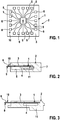
- FIG. 1 shows in a simplified plan view an interposer 1 for a in FIG. 1 not shown MID component 2.
- the interposer 1 has a flat circuit carrier 3, which is preferably formed as a flexible film. In the present case, the interposer 1 is thus designed as an interposer film.
- an electronic component 4 is arranged centrally, which is designed as an integrated circuit (IC) or as a chip.
- the component 4 is connected by conductor tracks 5, of which only a few are provided with reference numerals for reasons of clarity, with contact points 6, which are formed as contact pads. Also of the contact points 6 are provided for the reasons mentioned above, only a few with reference numerals.
- the contact points 6 are at the outer edge of the circuit substrate 3 substantially Due to the displacement of the contact points 6 to the outside, ie away from the component, they are further spaced from each other and can even be made larger, whereby the electrical contact of the component 4 is simplified.
- the interposer 1 or the circuit carrier 3 is preferably formed in two or more layers according to an embodiment not shown here, in order to further optimize the unbundling of the contact points of the component 4 and the circuit design. It is also conceivable to provide on the rear side of the circuit carrier 3, which is not visible here, further contact points and possibly also one or more electrical / electronic components.
- the component 4 is applied to the circuit carrier 3, for example, by flip-chip mounting technology.
- other electrical / electronic components can be applied to this side of the circuit substrate 3.
- the one or more components are formed thin to provide an overall thin structure and on the other to ensure a mounting flexibility.
- the contact points 6 and the contact plates are preferably coated with a noble surface, in order subsequently to be contacted with a silver conductive paste, for example.
- a suitable existing package with compatible technology can be used for the integration.
- FIGS. 2 to 5 show in schematic sectional views how the interposer 1 is used to produce the MID component 2. The manufacturing process thus begins with the provision of the interposer 1.
- the interposer 1 is held in the injection mold 8 such that an edge portion 9 with a row 10 of the contact points 6 is located outside of the injection mold 8, while the component 4 is arranged in particular within the injection mold.
- FIG. 3 shows the MID component 2 after the successful Umspritzvorgang, after removal from the injection molding tool 7. While the populated interposer 1 is essentially housed by the plastic extrusion 11, the edge region 9 remains outside the plastic extrusion, so that the contact points 6 of the contact row 10 are exposed and are contactable.
- LCP plastic liquid crystal polymer
- the now exposed edge portion 9 of the interposer 1 is flexible due to the interposer and can be easily deformed or bent, for example, for contacting.
- the edge portion 9 may form a connector strip which is insertable into a corresponding mating connector.
- the plastic extrusion coating 11 has cured, according to FIG. 4 at least one contact point 6, which is located within the plastic extrusion 11, the plastic removed again.
- the MID component 2 is subjected to laser processing by means of a laser tool 12.
- the plastic extrusion 11 is removed at the contact point 6 within the plastic extrusion 11 by laser drilling, whereby the underlying contact point 6 is exposed.
- the contact point 6 can be contacted within the plastic extrusion 11.
- the plastic extrusion 11 or the plastic at the points where an additional metallization is to be provided later are structured.
- the opening 13 is activated or metallized.
- a plasma method is preferred
- Jet method or a galvanic deposition method used.
- the material deposition can take place in combination with the metallization of the MID component.
- the opening 13 is formed as a via.
- the laser process can also be applied here using different MID structuring technologies before or after the metallization.
- the 2-component injection molding or hot stamping process is a possible alternative.
- FIG. 5 This is exemplified by the production of a via 14 by means of a jet process by means of a corresponding jetting tool 15.
- Metallization of printed conductors on the outer side of the MID component now takes place on the MID component 2 with the integrated component 4 whose contacts can be contacted via the contact points 6 2 performed, on the side on which the opening 13 is provided, so that the opening 13, in particular the feedthrough 14 can be connected directly to the conductor tracks.
- the printed conductors can be produced by laser direct structuring, electroplating, jet coating methods, metering technology or plasma coating methods.
- the electrical contact to the contact point 6 within the plastic extrusion 11 is produced directly or by means of the plated-through holes.
- the opening 13 is preferably produced by jet molding or dosing conductive pastes simultaneously, before or after the production of the printed conductors.
- the respective opening 13 can be metallized by filling with electrically conductive material at the same time by a Jettitle réelle in the process of producing the interconnects.
- the contact with the electrical components or with the respective contact point 6 is additionally produced.
- these contacts for example, by galvanizing conductive paste or galvanically reinforced. If a direct laser structuring is carried out with galvanic production of the printed conductors, then the electrical contacts are expediently produced in the same electroplating process as in the case of Deposition of the conductor tracks.
- the metal platelets or metal pads of the contact points 6 have a compatible metallization such as copper, a nickel-Pd coating or plasma-deposited copper, in particular without the isolated side wall of the opening 13 having a seeding or a plasma metal deposition.
- the circuit carrier 3 or the interposer 1 is preferably produced in a planar manner, whereby a subsequent deformation into a three-dimensional structure due to the flexible interposer foil, in particular before the encapsulation, is possible and preferred in order to produce a three-dimensionally shaped MID component 2.
- manufacturing costs are reduced in the production of three-dimensional MID components.
- Silicones or thermoplastics may also be used as substrate materials to obtain a stretchable or plastically deformable substrate.
- the layer structure of the MID component 2 is designed in such a way that its shaping can be realized by plastic deformation, for example by an embossing process, then the realization of the interposer 1 in three-dimensional form is possible and thus a design as an adapted insert part is made available at low cost.
- the interposer 1 moreover provides an additional area for large area contacting processes with an electronic environment, for example plug connectors, clamping contacts or the like, in particular also through the free edge section 9.
Landscapes
- Engineering & Computer Science (AREA)
- Manufacturing & Machinery (AREA)
- Microelectronics & Electronic Packaging (AREA)
- Structure Of Printed Boards (AREA)
Claims (10)
- Composant MID (2) pour un appareil de commande ou un capteur, en particulier d'un véhicule, présentant un porte-circuit (3) et une encapsulation (11) en matière synthétique qui englobe au moins certaines parties du porte-circuit (3), caractérisé en ce que le porte-circuit (3) est configuré comme intercalaire flexible (1) qui équipé d'au moins un composant électrique/électronique (4) et présente au moins un emplacement de contact (6) électriquement conducteur et en ce qu'une section (9) de l'intercalaire (1) qui présente l'emplacement de contact (6) est disposée à l'extérieur de l'encapsulation (11) en matière synthétique.
- Composant selon la revendication 1, caractérisé en ce que la section (9) est une partie de bord de l'intercalaire (1).
- Composant selon l'une des revendications précédentes, caractérisé en ce que l'intercalaire (1) est configuré en tant que feuille d'intercalaire.
- Composant selon l'une des revendications précédentes, caractérisé en ce que le composant électrique/électronique (4) est encapsulé dans l'encapsulation (11) en matière synthétique.
- Composant selon l'une des revendications précédentes, caractérisé en ce que l'intercalaire (1) présente au moins un autre emplacement de contact disposé à l'intérieur de l'encapsulation (11) en matière synthétique et peut être libéré ou est libéré par traitement, en particulier par traitement au laser de l'encapsulation (11) en matière synthétique.
- Procédé de fabrication d'un composant MID (2), en particulier selon l'une des revendications précédentes, le procédé présentant les étapes suivantes :- préparer un intercalaire flexible (1) qui présente au moins un emplacement de contact (6) électriquement conducteur,- appliquer au moins un composant électrique/électronique (4) sur l'intercalaire (1) en vue de former un intercalaire équipé,- englober l'intercalaire équipé dans une matière synthétique de telle sorte qu'une section (9) de l'intercalaire (1) qui présente l'emplacement de contact (6) soit située à l'extérieur de l'encapsulation (11) en matière synthétique.
- Procédé selon la revendication 6, caractérisé en ce qu'on utilise en tant qu'intercalaire (1) une feuille d'intercalaire.
- Procédé selon l'une des revendications précédentes, caractérisé en ce que l'intercalaire est équipé d'au moins un autre emplacement de contact (6) englobé dans l'encapsulation (11) en matière synthétique.
- Procédé selon la revendication 8, caractérisé en ce que l'autre emplacement de contact situé à l'intérieur de l'encapsulation (11) en matière synthétique est libéré en ménageant une ouverture (13) dans l'encapsulation (11) en matière synthétique.
- Procédé selon la revendication 9, caractérisé en ce que l'ouverture (13) est ménagée par traitement au laser de l'encapsulation (11) en matière synthétique.
Applications Claiming Priority (1)
| Application Number | Priority Date | Filing Date | Title |
|---|---|---|---|
| DE102013212254.3A DE102013212254A1 (de) | 2013-06-26 | 2013-06-26 | MID-Bauteil, Verfahren zur Herstellung |
Publications (2)
| Publication Number | Publication Date |
|---|---|
| EP2819492A1 EP2819492A1 (fr) | 2014-12-31 |
| EP2819492B1 true EP2819492B1 (fr) | 2018-03-28 |
Family
ID=50933002
Family Applications (1)
| Application Number | Title | Priority Date | Filing Date |
|---|---|---|---|
| EP14171870.0A Active EP2819492B1 (fr) | 2013-06-26 | 2014-06-11 | Composant MID, procédé de fabrication |
Country Status (2)
| Country | Link |
|---|---|
| EP (1) | EP2819492B1 (fr) |
| DE (1) | DE102013212254A1 (fr) |
Families Citing this family (7)
| Publication number | Priority date | Publication date | Assignee | Title |
|---|---|---|---|---|
| JP6016965B2 (ja) | 2015-03-02 | 2016-10-26 | 三菱電機株式会社 | 電子機器ユニット及びその製造金型装置 |
| DE102015122120A1 (de) | 2015-12-17 | 2017-06-22 | Dirk Pylarski | Schweißelement zum Verbinden mit wenigstens einem Rohrleitungselement |
| DE102015226201A1 (de) | 2015-12-21 | 2017-06-22 | Robert Bosch Gmbh | Elektrische Schaltung, Verfahren zum Herstellen einer elektrischen Schaltung und Karosserieteil für ein Fahrzeug |
| DE102015226137A1 (de) | 2015-12-21 | 2017-06-22 | Robert Bosch Gmbh | Verfahren zum Herstellen eines Schaltungsbauteils und Schaltungsbauteil |
| DE102015226192A1 (de) | 2015-12-21 | 2017-06-22 | Robert Bosch Gmbh | Verfahren zum Herstellen einer elektrischen Schaltung, Verfahren zum Befestigen einer elektrischen Schaltung und elektrische Schaltung |
| DE102016220065A1 (de) * | 2016-10-14 | 2018-04-19 | Robert Bosch Gmbh | Verfahren zum Ausbilden mindestens eines Wärmeableitpfades für ein mikroelektronisches Bauteil und entsprechendes mikroelektronisches Bauteil |
| DE102019201035A1 (de) * | 2019-01-28 | 2020-07-30 | Robert Bosch Gmbh | Verfahren zur Behandlung metallischer Einlegeteile |
Family Cites Families (3)
| Publication number | Priority date | Publication date | Assignee | Title |
|---|---|---|---|---|
| DE102007029913A1 (de) * | 2007-06-28 | 2009-01-02 | Robert Bosch Gmbh | Elektrisches Steuergerät |
| DE102007031980A1 (de) * | 2007-07-10 | 2009-01-15 | Robert Bosch Gmbh | Anschlusseinheit für eine Druckmesszelle |
| DE102010041121A1 (de) | 2010-09-21 | 2012-03-22 | Robert Bosch Gmbh | Schaltungsträger sowie Verfahren zur Herstellung eines Schaltungsträgers |
-
2013
- 2013-06-26 DE DE102013212254.3A patent/DE102013212254A1/de not_active Withdrawn
-
2014
- 2014-06-11 EP EP14171870.0A patent/EP2819492B1/fr active Active
Non-Patent Citations (1)
| Title |
|---|
| None * |
Also Published As
| Publication number | Publication date |
|---|---|
| DE102013212254A1 (de) | 2014-12-31 |
| EP2819492A1 (fr) | 2014-12-31 |
Similar Documents
| Publication | Publication Date | Title |
|---|---|---|
| EP2819492B1 (fr) | Composant MID, procédé de fabrication | |
| EP2595249B1 (fr) | Borne de connexion | |
| DE102006018902B4 (de) | Elektronisches Schaltungsgerät und Verfahren zur Herstellung desselben | |
| EP3443825B1 (fr) | Procédé de positionnement de cartes de circuit imprimé et ensemble de cartes de circuit imprimé | |
| DE102008045615C5 (de) | Verfahren zur Herstellung eines Leistungshalbleitermoduls | |
| EP1351551B1 (fr) | Dispositif de contact pour prothèse auditive | |
| DE102010039063B4 (de) | Sensormodul mit einem elektromagnetisch abgeschirmten elektrischen Bauteil und Verfahren zur Herstellung eines solchen Sensormoduls | |
| EP2289100A2 (fr) | Procédé de fabrication d'un module électronique | |
| DE102009024385A1 (de) | Verfahren zur Herstellung eines Leistungshalbleitermoduls und Leistungshalbleitermodul mit einer Verbindungseinrichtung | |
| DE102008058003A1 (de) | Halbleitermodul und Verfahren zu dessen Herstellung | |
| DE102013201417A1 (de) | Verfahren zur Herstellung eines MID-Bauteils, MID-Bauteil | |
| DE102014200936A1 (de) | Elektronikbaugruppe | |
| DE102017206217A1 (de) | Elektrische Kontaktanordnung | |
| DE102016218970A1 (de) | Elektronikmodul und Verfahren zur Herstellung eines Elektronikmoduls | |
| DE102010041121A1 (de) | Schaltungsträger sowie Verfahren zur Herstellung eines Schaltungsträgers | |
| EP3520585B1 (fr) | Procédé de fabrication d'un composant électronique et composant électronique, en particulier pour un module de commande de boîte de vitesses | |
| EP2340693B1 (fr) | Procédé de fabrication d'un circuit électrique | |
| DE102006041610B3 (de) | Metallisierte Kunststoffoberfläche und Verfahren zum Bearbeiten von metallisierten Kunststoffoberflächen | |
| DE29619867U1 (de) | Elektrisches Schalt- und Steuergerät | |
| DE102007037841A1 (de) | Trägermodul und Verfahren zur Herstellung eines Trägermoduls | |
| DE102016208928A1 (de) | Verfahren zur elektrischen Kontaktierung eines MID-Bauteils | |
| DE19742470A1 (de) | Verfahren zum Herstellen eines elektrischen Gerätes mit Gehäuse | |
| DE10333967A1 (de) | Anordnung zum Führen von elektrischen Leiterbahnen | |
| DE102006025553B4 (de) | Verfahren zum Herstellen einer elektronischen Baueinheit | |
| EP3526159A1 (fr) | Dispositif capteur de pression micromécanique et procédé de fabrication correspondant |
Legal Events
| Date | Code | Title | Description |
|---|---|---|---|
| PUAI | Public reference made under article 153(3) epc to a published international application that has entered the european phase |
Free format text: ORIGINAL CODE: 0009012 |
|
| 17P | Request for examination filed |
Effective date: 20140611 |
|
| AK | Designated contracting states |
Kind code of ref document: A1 Designated state(s): AL AT BE BG CH CY CZ DE DK EE ES FI FR GB GR HR HU IE IS IT LI LT LU LV MC MK MT NL NO PL PT RO RS SE SI SK SM TR |
|
| AX | Request for extension of the european patent |
Extension state: BA ME |
|
| R17P | Request for examination filed (corrected) |
Effective date: 20150630 |
|
| RBV | Designated contracting states (corrected) |
Designated state(s): AL AT BE BG CH CY CZ DE DK EE ES FI FR GB GR HR HU IE IS IT LI LT LU LV MC MK MT NL NO PL PT RO RS SE SI SK SM TR |
|
| GRAP | Despatch of communication of intention to grant a patent |
Free format text: ORIGINAL CODE: EPIDOSNIGR1 |
|
| INTG | Intention to grant announced |
Effective date: 20171122 |
|
| GRAS | Grant fee paid |
Free format text: ORIGINAL CODE: EPIDOSNIGR3 |
|
| GRAA | (expected) grant |
Free format text: ORIGINAL CODE: 0009210 |
|
| AK | Designated contracting states |
Kind code of ref document: B1 Designated state(s): AL AT BE BG CH CY CZ DE DK EE ES FI FR GB GR HR HU IE IS IT LI LT LU LV MC MK MT NL NO PL PT RO RS SE SI SK SM TR |
|
| REG | Reference to a national code |
Ref country code: GB Ref legal event code: FG4D Free format text: NOT ENGLISH |
|
| REG | Reference to a national code |
Ref country code: CH Ref legal event code: EP |
|
| REG | Reference to a national code |
Ref country code: AT Ref legal event code: REF Ref document number: 984536 Country of ref document: AT Kind code of ref document: T Effective date: 20180415 |
|
| REG | Reference to a national code |
Ref country code: IE Ref legal event code: FG4D Free format text: LANGUAGE OF EP DOCUMENT: GERMAN |
|
| REG | Reference to a national code |
Ref country code: DE Ref legal event code: R096 Ref document number: 502014007736 Country of ref document: DE |
|
| REG | Reference to a national code |
Ref country code: NL Ref legal event code: FP |
|
| REG | Reference to a national code |
Ref country code: FR Ref legal event code: PLFP Year of fee payment: 5 |
|
| PG25 | Lapsed in a contracting state [announced via postgrant information from national office to epo] |
Ref country code: LT Free format text: LAPSE BECAUSE OF FAILURE TO SUBMIT A TRANSLATION OF THE DESCRIPTION OR TO PAY THE FEE WITHIN THE PRESCRIBED TIME-LIMIT Effective date: 20180328 Ref country code: FI Free format text: LAPSE BECAUSE OF FAILURE TO SUBMIT A TRANSLATION OF THE DESCRIPTION OR TO PAY THE FEE WITHIN THE PRESCRIBED TIME-LIMIT Effective date: 20180328 Ref country code: HR Free format text: LAPSE BECAUSE OF FAILURE TO SUBMIT A TRANSLATION OF THE DESCRIPTION OR TO PAY THE FEE WITHIN THE PRESCRIBED TIME-LIMIT Effective date: 20180328 Ref country code: NO Free format text: LAPSE BECAUSE OF FAILURE TO SUBMIT A TRANSLATION OF THE DESCRIPTION OR TO PAY THE FEE WITHIN THE PRESCRIBED TIME-LIMIT Effective date: 20180628 |
|
| REG | Reference to a national code |
Ref country code: LT Ref legal event code: MG4D |
|
| PG25 | Lapsed in a contracting state [announced via postgrant information from national office to epo] |
Ref country code: GR Free format text: LAPSE BECAUSE OF FAILURE TO SUBMIT A TRANSLATION OF THE DESCRIPTION OR TO PAY THE FEE WITHIN THE PRESCRIBED TIME-LIMIT Effective date: 20180629 Ref country code: BG Free format text: LAPSE BECAUSE OF FAILURE TO SUBMIT A TRANSLATION OF THE DESCRIPTION OR TO PAY THE FEE WITHIN THE PRESCRIBED TIME-LIMIT Effective date: 20180628 Ref country code: RS Free format text: LAPSE BECAUSE OF FAILURE TO SUBMIT A TRANSLATION OF THE DESCRIPTION OR TO PAY THE FEE WITHIN THE PRESCRIBED TIME-LIMIT Effective date: 20180328 Ref country code: SE Free format text: LAPSE BECAUSE OF FAILURE TO SUBMIT A TRANSLATION OF THE DESCRIPTION OR TO PAY THE FEE WITHIN THE PRESCRIBED TIME-LIMIT Effective date: 20180328 Ref country code: LV Free format text: LAPSE BECAUSE OF FAILURE TO SUBMIT A TRANSLATION OF THE DESCRIPTION OR TO PAY THE FEE WITHIN THE PRESCRIBED TIME-LIMIT Effective date: 20180328 |
|
| PG25 | Lapsed in a contracting state [announced via postgrant information from national office to epo] |
Ref country code: MT Free format text: LAPSE BECAUSE OF FAILURE TO SUBMIT A TRANSLATION OF THE DESCRIPTION OR TO PAY THE FEE WITHIN THE PRESCRIBED TIME-LIMIT Effective date: 20180328 |
|
| PG25 | Lapsed in a contracting state [announced via postgrant information from national office to epo] |
Ref country code: IT Free format text: LAPSE BECAUSE OF FAILURE TO SUBMIT A TRANSLATION OF THE DESCRIPTION OR TO PAY THE FEE WITHIN THE PRESCRIBED TIME-LIMIT Effective date: 20180328 Ref country code: RO Free format text: LAPSE BECAUSE OF FAILURE TO SUBMIT A TRANSLATION OF THE DESCRIPTION OR TO PAY THE FEE WITHIN THE PRESCRIBED TIME-LIMIT Effective date: 20180328 Ref country code: ES Free format text: LAPSE BECAUSE OF FAILURE TO SUBMIT A TRANSLATION OF THE DESCRIPTION OR TO PAY THE FEE WITHIN THE PRESCRIBED TIME-LIMIT Effective date: 20180328 Ref country code: EE Free format text: LAPSE BECAUSE OF FAILURE TO SUBMIT A TRANSLATION OF THE DESCRIPTION OR TO PAY THE FEE WITHIN THE PRESCRIBED TIME-LIMIT Effective date: 20180328 Ref country code: PL Free format text: LAPSE BECAUSE OF FAILURE TO SUBMIT A TRANSLATION OF THE DESCRIPTION OR TO PAY THE FEE WITHIN THE PRESCRIBED TIME-LIMIT Effective date: 20180328 Ref country code: AL Free format text: LAPSE BECAUSE OF FAILURE TO SUBMIT A TRANSLATION OF THE DESCRIPTION OR TO PAY THE FEE WITHIN THE PRESCRIBED TIME-LIMIT Effective date: 20180328 |
|
| PG25 | Lapsed in a contracting state [announced via postgrant information from national office to epo] |
Ref country code: SM Free format text: LAPSE BECAUSE OF FAILURE TO SUBMIT A TRANSLATION OF THE DESCRIPTION OR TO PAY THE FEE WITHIN THE PRESCRIBED TIME-LIMIT Effective date: 20180328 Ref country code: SK Free format text: LAPSE BECAUSE OF FAILURE TO SUBMIT A TRANSLATION OF THE DESCRIPTION OR TO PAY THE FEE WITHIN THE PRESCRIBED TIME-LIMIT Effective date: 20180328 Ref country code: CZ Free format text: LAPSE BECAUSE OF FAILURE TO SUBMIT A TRANSLATION OF THE DESCRIPTION OR TO PAY THE FEE WITHIN THE PRESCRIBED TIME-LIMIT Effective date: 20180328 |
|
| PG25 | Lapsed in a contracting state [announced via postgrant information from national office to epo] |
Ref country code: PT Free format text: LAPSE BECAUSE OF FAILURE TO SUBMIT A TRANSLATION OF THE DESCRIPTION OR TO PAY THE FEE WITHIN THE PRESCRIBED TIME-LIMIT Effective date: 20180730 |
|
| REG | Reference to a national code |
Ref country code: DE Ref legal event code: R097 Ref document number: 502014007736 Country of ref document: DE |
|
| PG25 | Lapsed in a contracting state [announced via postgrant information from national office to epo] |
Ref country code: DK Free format text: LAPSE BECAUSE OF FAILURE TO SUBMIT A TRANSLATION OF THE DESCRIPTION OR TO PAY THE FEE WITHIN THE PRESCRIBED TIME-LIMIT Effective date: 20180328 |
|
| REG | Reference to a national code |
Ref country code: CH Ref legal event code: PL |
|
| PLBE | No opposition filed within time limit |
Free format text: ORIGINAL CODE: 0009261 |
|
| STAA | Information on the status of an ep patent application or granted ep patent |
Free format text: STATUS: NO OPPOSITION FILED WITHIN TIME LIMIT |
|
| 26N | No opposition filed |
Effective date: 20190103 |
|
| REG | Reference to a national code |
Ref country code: BE Ref legal event code: MM Effective date: 20180630 |
|
| REG | Reference to a national code |
Ref country code: IE Ref legal event code: MM4A |
|
| PG25 | Lapsed in a contracting state [announced via postgrant information from national office to epo] |
Ref country code: MC Free format text: LAPSE BECAUSE OF FAILURE TO SUBMIT A TRANSLATION OF THE DESCRIPTION OR TO PAY THE FEE WITHIN THE PRESCRIBED TIME-LIMIT Effective date: 20180328 Ref country code: LU Free format text: LAPSE BECAUSE OF NON-PAYMENT OF DUE FEES Effective date: 20180611 |
|
| PG25 | Lapsed in a contracting state [announced via postgrant information from national office to epo] |
Ref country code: IE Free format text: LAPSE BECAUSE OF NON-PAYMENT OF DUE FEES Effective date: 20180611 Ref country code: LI Free format text: LAPSE BECAUSE OF NON-PAYMENT OF DUE FEES Effective date: 20180630 Ref country code: CH Free format text: LAPSE BECAUSE OF NON-PAYMENT OF DUE FEES Effective date: 20180630 |
|
| PG25 | Lapsed in a contracting state [announced via postgrant information from national office to epo] |
Ref country code: SI Free format text: LAPSE BECAUSE OF FAILURE TO SUBMIT A TRANSLATION OF THE DESCRIPTION OR TO PAY THE FEE WITHIN THE PRESCRIBED TIME-LIMIT Effective date: 20180328 Ref country code: BE Free format text: LAPSE BECAUSE OF NON-PAYMENT OF DUE FEES Effective date: 20180630 |
|
| PG25 | Lapsed in a contracting state [announced via postgrant information from national office to epo] |
Ref country code: TR Free format text: LAPSE BECAUSE OF FAILURE TO SUBMIT A TRANSLATION OF THE DESCRIPTION OR TO PAY THE FEE WITHIN THE PRESCRIBED TIME-LIMIT Effective date: 20180328 |
|
| PG25 | Lapsed in a contracting state [announced via postgrant information from national office to epo] |
Ref country code: HU Free format text: LAPSE BECAUSE OF FAILURE TO SUBMIT A TRANSLATION OF THE DESCRIPTION OR TO PAY THE FEE WITHIN THE PRESCRIBED TIME-LIMIT; INVALID AB INITIO Effective date: 20140611 |
|
| PG25 | Lapsed in a contracting state [announced via postgrant information from national office to epo] |
Ref country code: CY Free format text: LAPSE BECAUSE OF FAILURE TO SUBMIT A TRANSLATION OF THE DESCRIPTION OR TO PAY THE FEE WITHIN THE PRESCRIBED TIME-LIMIT Effective date: 20180328 Ref country code: MK Free format text: LAPSE BECAUSE OF NON-PAYMENT OF DUE FEES Effective date: 20180328 |
|
| PG25 | Lapsed in a contracting state [announced via postgrant information from national office to epo] |
Ref country code: IS Free format text: LAPSE BECAUSE OF FAILURE TO SUBMIT A TRANSLATION OF THE DESCRIPTION OR TO PAY THE FEE WITHIN THE PRESCRIBED TIME-LIMIT Effective date: 20180728 |
|
| REG | Reference to a national code |
Ref country code: AT Ref legal event code: MM01 Ref document number: 984536 Country of ref document: AT Kind code of ref document: T Effective date: 20190611 |
|
| PG25 | Lapsed in a contracting state [announced via postgrant information from national office to epo] |
Ref country code: AT Free format text: LAPSE BECAUSE OF NON-PAYMENT OF DUE FEES Effective date: 20190611 |
|
| PGFP | Annual fee paid to national office [announced via postgrant information from national office to epo] |
Ref country code: NL Payment date: 20230620 Year of fee payment: 10 Ref country code: FR Payment date: 20230621 Year of fee payment: 10 |
|
| PGFP | Annual fee paid to national office [announced via postgrant information from national office to epo] |
Ref country code: GB Payment date: 20230622 Year of fee payment: 10 |
|
| REG | Reference to a national code |
Ref country code: NL Ref legal event code: MM Effective date: 20240701 |
|
| GBPC | Gb: european patent ceased through non-payment of renewal fee |
Effective date: 20240611 |
|
| PG25 | Lapsed in a contracting state [announced via postgrant information from national office to epo] |
Ref country code: NL Free format text: LAPSE BECAUSE OF NON-PAYMENT OF DUE FEES Effective date: 20240701 |
|
| PG25 | Lapsed in a contracting state [announced via postgrant information from national office to epo] |
Ref country code: NL Free format text: LAPSE BECAUSE OF NON-PAYMENT OF DUE FEES Effective date: 20240701 |
|
| PG25 | Lapsed in a contracting state [announced via postgrant information from national office to epo] |
Ref country code: FR Free format text: LAPSE BECAUSE OF NON-PAYMENT OF DUE FEES Effective date: 20240630 |
|
| PG25 | Lapsed in a contracting state [announced via postgrant information from national office to epo] |
Ref country code: GB Free format text: LAPSE BECAUSE OF NON-PAYMENT OF DUE FEES Effective date: 20240611 |
|
| PGFP | Annual fee paid to national office [announced via postgrant information from national office to epo] |
Ref country code: DE Payment date: 20250814 Year of fee payment: 12 |