EP2820683B1 - Panneau solaire en silicium cristallin biface avec réflecteur - Google Patents
Panneau solaire en silicium cristallin biface avec réflecteur Download PDFInfo
- Publication number
- EP2820683B1 EP2820683B1 EP13754110.8A EP13754110A EP2820683B1 EP 2820683 B1 EP2820683 B1 EP 2820683B1 EP 13754110 A EP13754110 A EP 13754110A EP 2820683 B1 EP2820683 B1 EP 2820683B1
- Authority
- EP
- European Patent Office
- Prior art keywords
- row
- layer
- solar cells
- rows
- long axis
- Prior art date
- Legal status (The legal status is an assumption and is not a legal conclusion. Google has not performed a legal analysis and makes no representation as to the accuracy of the status listed.)
- Active
Links
Images




Classifications
-
- H—ELECTRICITY
- H10—SEMICONDUCTOR DEVICES; ELECTRIC SOLID-STATE DEVICES NOT OTHERWISE PROVIDED FOR
- H10F—INORGANIC SEMICONDUCTOR DEVICES SENSITIVE TO INFRARED RADIATION, LIGHT, ELECTROMAGNETIC RADIATION OF SHORTER WAVELENGTH OR CORPUSCULAR RADIATION
- H10F10/00—Individual photovoltaic cells, e.g. solar cells
- H10F10/10—Individual photovoltaic cells, e.g. solar cells having potential barriers
- H10F10/14—Photovoltaic cells having only PN homojunction potential barriers
-
- H—ELECTRICITY
- H10—SEMICONDUCTOR DEVICES; ELECTRIC SOLID-STATE DEVICES NOT OTHERWISE PROVIDED FOR
- H10F—INORGANIC SEMICONDUCTOR DEVICES SENSITIVE TO INFRARED RADIATION, LIGHT, ELECTROMAGNETIC RADIATION OF SHORTER WAVELENGTH OR CORPUSCULAR RADIATION
- H10F10/00—Individual photovoltaic cells, e.g. solar cells
- H10F10/10—Individual photovoltaic cells, e.g. solar cells having potential barriers
- H10F10/14—Photovoltaic cells having only PN homojunction potential barriers
- H10F10/148—Double-emitter photovoltaic cells, e.g. bifacial photovoltaic cells
-
- H—ELECTRICITY
- H10—SEMICONDUCTOR DEVICES; ELECTRIC SOLID-STATE DEVICES NOT OTHERWISE PROVIDED FOR
- H10F—INORGANIC SEMICONDUCTOR DEVICES SENSITIVE TO INFRARED RADIATION, LIGHT, ELECTROMAGNETIC RADIATION OF SHORTER WAVELENGTH OR CORPUSCULAR RADIATION
- H10F19/00—Integrated devices, or assemblies of multiple devices, comprising at least one photovoltaic cell covered by group H10F10/00, e.g. photovoltaic modules
- H10F19/80—Encapsulations or containers for integrated devices, or assemblies of multiple devices, having photovoltaic cells
- H10F19/807—Double-glass encapsulation, e.g. photovoltaic cells arranged between front and rear glass sheets
-
- H—ELECTRICITY
- H10—SEMICONDUCTOR DEVICES; ELECTRIC SOLID-STATE DEVICES NOT OTHERWISE PROVIDED FOR
- H10F—INORGANIC SEMICONDUCTOR DEVICES SENSITIVE TO INFRARED RADIATION, LIGHT, ELECTROMAGNETIC RADIATION OF SHORTER WAVELENGTH OR CORPUSCULAR RADIATION
- H10F19/00—Integrated devices, or assemblies of multiple devices, comprising at least one photovoltaic cell covered by group H10F10/00, e.g. photovoltaic modules
- H10F19/90—Structures for connecting between photovoltaic cells, e.g. interconnections or insulating spacers
- H10F19/902—Structures for connecting between photovoltaic cells, e.g. interconnections or insulating spacers for series or parallel connection of photovoltaic cells
-
- H—ELECTRICITY
- H10—SEMICONDUCTOR DEVICES; ELECTRIC SOLID-STATE DEVICES NOT OTHERWISE PROVIDED FOR
- H10F—INORGANIC SEMICONDUCTOR DEVICES SENSITIVE TO INFRARED RADIATION, LIGHT, ELECTROMAGNETIC RADIATION OF SHORTER WAVELENGTH OR CORPUSCULAR RADIATION
- H10F77/00—Constructional details of devices covered by this subclass
- H10F77/20—Electrodes
- H10F77/206—Electrodes for devices having potential barriers
- H10F77/211—Electrodes for devices having potential barriers for photovoltaic cells
-
- H—ELECTRICITY
- H10—SEMICONDUCTOR DEVICES; ELECTRIC SOLID-STATE DEVICES NOT OTHERWISE PROVIDED FOR
- H10F—INORGANIC SEMICONDUCTOR DEVICES SENSITIVE TO INFRARED RADIATION, LIGHT, ELECTROMAGNETIC RADIATION OF SHORTER WAVELENGTH OR CORPUSCULAR RADIATION
- H10F77/00—Constructional details of devices covered by this subclass
- H10F77/20—Electrodes
- H10F77/206—Electrodes for devices having potential barriers
- H10F77/211—Electrodes for devices having potential barriers for photovoltaic cells
- H10F77/215—Geometries of grid contacts
-
- H—ELECTRICITY
- H10—SEMICONDUCTOR DEVICES; ELECTRIC SOLID-STATE DEVICES NOT OTHERWISE PROVIDED FOR
- H10F—INORGANIC SEMICONDUCTOR DEVICES SENSITIVE TO INFRARED RADIATION, LIGHT, ELECTROMAGNETIC RADIATION OF SHORTER WAVELENGTH OR CORPUSCULAR RADIATION
- H10F77/00—Constructional details of devices covered by this subclass
- H10F77/20—Electrodes
- H10F77/244—Electrodes made of transparent conductive layers, e.g. transparent conductive oxide [TCO] layers
-
- H—ELECTRICITY
- H10—SEMICONDUCTOR DEVICES; ELECTRIC SOLID-STATE DEVICES NOT OTHERWISE PROVIDED FOR
- H10F—INORGANIC SEMICONDUCTOR DEVICES SENSITIVE TO INFRARED RADIATION, LIGHT, ELECTROMAGNETIC RADIATION OF SHORTER WAVELENGTH OR CORPUSCULAR RADIATION
- H10F77/00—Constructional details of devices covered by this subclass
- H10F77/30—Coatings
- H10F77/306—Coatings for devices having potential barriers
- H10F77/311—Coatings for devices having potential barriers for photovoltaic cells
-
- H—ELECTRICITY
- H10—SEMICONDUCTOR DEVICES; ELECTRIC SOLID-STATE DEVICES NOT OTHERWISE PROVIDED FOR
- H10F—INORGANIC SEMICONDUCTOR DEVICES SENSITIVE TO INFRARED RADIATION, LIGHT, ELECTROMAGNETIC RADIATION OF SHORTER WAVELENGTH OR CORPUSCULAR RADIATION
- H10F77/00—Constructional details of devices covered by this subclass
- H10F77/40—Optical elements or arrangements
- H10F77/42—Optical elements or arrangements directly associated or integrated with photovoltaic cells, e.g. light-reflecting means or light-concentrating means
- H10F77/488—Reflecting light-concentrating means, e.g. parabolic mirrors or concentrators using total internal reflection
-
- H—ELECTRICITY
- H10—SEMICONDUCTOR DEVICES; ELECTRIC SOLID-STATE DEVICES NOT OTHERWISE PROVIDED FOR
- H10F—INORGANIC SEMICONDUCTOR DEVICES SENSITIVE TO INFRARED RADIATION, LIGHT, ELECTROMAGNETIC RADIATION OF SHORTER WAVELENGTH OR CORPUSCULAR RADIATION
- H10F77/00—Constructional details of devices covered by this subclass
- H10F77/60—Arrangements for cooling, heating, ventilating or compensating for temperature fluctuations
- H10F77/63—Arrangements for cooling directly associated or integrated with photovoltaic cells, e.g. heat sinks directly associated with the photovoltaic cells or integrated Peltier elements for active cooling
- H10F77/67—Arrangements for cooling directly associated or integrated with photovoltaic cells, e.g. heat sinks directly associated with the photovoltaic cells or integrated Peltier elements for active cooling including means to utilise heat energy directly associated with the photovoltaic cells, e.g. integrated Seebeck elements
-
- Y—GENERAL TAGGING OF NEW TECHNOLOGICAL DEVELOPMENTS; GENERAL TAGGING OF CROSS-SECTIONAL TECHNOLOGIES SPANNING OVER SEVERAL SECTIONS OF THE IPC; TECHNICAL SUBJECTS COVERED BY FORMER USPC CROSS-REFERENCE ART COLLECTIONS [XRACs] AND DIGESTS
- Y02—TECHNOLOGIES OR APPLICATIONS FOR MITIGATION OR ADAPTATION AGAINST CLIMATE CHANGE
- Y02E—REDUCTION OF GREENHOUSE GAS [GHG] EMISSIONS, RELATED TO ENERGY GENERATION, TRANSMISSION OR DISTRIBUTION
- Y02E10/00—Energy generation through renewable energy sources
- Y02E10/50—Photovoltaic [PV] energy
- Y02E10/52—PV systems with concentrators
-
- Y—GENERAL TAGGING OF NEW TECHNOLOGICAL DEVELOPMENTS; GENERAL TAGGING OF CROSS-SECTIONAL TECHNOLOGIES SPANNING OVER SEVERAL SECTIONS OF THE IPC; TECHNICAL SUBJECTS COVERED BY FORMER USPC CROSS-REFERENCE ART COLLECTIONS [XRACs] AND DIGESTS
- Y02—TECHNOLOGIES OR APPLICATIONS FOR MITIGATION OR ADAPTATION AGAINST CLIMATE CHANGE
- Y02E—REDUCTION OF GREENHOUSE GAS [GHG] EMISSIONS, RELATED TO ENERGY GENERATION, TRANSMISSION OR DISTRIBUTION
- Y02E10/00—Energy generation through renewable energy sources
- Y02E10/50—Photovoltaic [PV] energy
- Y02E10/547—Monocrystalline silicon PV cells
Definitions
- Photovoltaic panels can be made to convert sunlight into electricity.
- photovoltaic panels can be made to convert sunlight into electricity.
- technologies for making photovoltaic panels including mono-crystalline silicon wafer based, multi-crystalline silicon wafer based, and thin film silicon based.
- Many commercially available photovoltaic panels are made with only one side exposed to sunlight.
- US 2011/0277819 dislcoses a photovoltaic system comprising solar cell panels and reflectors.
- the present disclosure relates to improved photovoltaic solar cell systems as defined in claim 1.
- a photovoltaic system having a solar panel and at least two reflectors is disclosed.
- the solar panel includes solar cells, at least some of which are bifacial solar cells.
- the solar cells are arranged in the panel to form at least four rows.
- the first row of solar cells is electrically connected in series.
- the first row of solar cells has a first long axis.
- the second row of solar cells is electrically connected in series.
- the second row of solar cells has a second long axis parallel to the first long axis.
- the first row of solar cells is electrically connected to the second row of solar cells in parallel.
- the first reflector is located proximal the solar panel.
- the first reflector includes a reflective surface facing the solar panel.
- the reflective surface has a third long axis that is parallel to the first and second long axes. In one embodiment, the third long axis forms an angle of from 5° to negative 5° to the first and second long axes.
- the reflective surface may comprise at least one of aluminum, silver, and/or a white colored material. In one embodiment, the reflective surface may have a compound-parabolic-shaped profile. In other embodiments, the reflective surface may have a semicircular-shaped profile, or a profile comprising planar surfaces.
- the solar panel may further include a first transparent protective layer and/or a second transparent protective layer. The solar cells in the solar panel may be disposed between the first transparent protective layer and the second transparent protective layer.
- the first transparent protective layer may be coupled to the plurality of first metal conductivity lines of the bifacial solar cells via a first lamination layer.
- the second transparent protective layer may be coupled to the plurality of second metal conductivity lines of the bifacial solar cells via a second lamination layer.
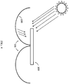
- the system includes a solar panel 100 and a reflector 120 located proximal the solar panel 100.
- the solar panel 100 includes a plurality of bifacial solar cells 110 arranged in two adjacent rows 112, 114.
- bifacial solar cell means a semiconductor-based solar cell having an upper surface and a lower surface, wherein both the upper and lower surfaces are photoactive.
- photoactive means capable of responding to light photoelectrically.
- the first row of bifacial solar cells 112 has a first long axis 113.
- the second row of bifacial solar cells 114 has a second long axis 115.
- the reflector 120 includes at least one reflective surface 130 facing the panel 100.
- the reflective surface 130 has a third long axis 132.
- the reflector 120 is configured to promote reflection of solar radiation (sunlight) towards the panel 100.
- the first row 112 is located proximal to the second row 114 such that the first long axis 113 is parallel to the second long axis 115.
- the reflector 120 is oriented such that the third long axis 132 is parallel to both the first and second long axes 113, 115.
- parallel means approximately parallel.
- a first line may be parallel to the long axis of a reflector (e.g., forming an angle from about 15° to about negative 15° to the long axis of the reflector).
- the bifacial solar cells 110 of the first row 112 are electrically connected to one another in series.
- the bifacial solar cells 110 of the second row 114 are electrically connected to one another in series.
- the first row 112 is electrically connected to the second row 114 in parallel.
- the bifacial solar cells 110 are configured such that each cell has a useful voltage, generally on the order of from about 0.5V to about 1.5V.
- the illustrated bifacial solar panel system can absorb light from both sides and over a larger area than the area of the panel itself. This is facilitated through the use of the reflector 120 that reflects sunlight toward the underside of the solar panel 100. Furthermore, the reflective surface 130 having a long axis 132 may facilitate the reflection of sunlight onto the underside of the solar panel 100 such that the amount of reflected sunlight incident on the panel is essentially uniform across the panel in a direction parallel to the long axis 132, yet highly non-uniform across the panel in a direction perpendicular to the long axis 132. As described above, the cells within the rows 112, 114 are electrically connected to one another in series, and the rows 112, 114 are electrically connected to one another in parallel.
- the rows 112, 114 are arranged with their long axes 113, 115 being coincidental to the long axis of the reflector 132.
- the bifacial solar cells 110 are oriented to allow each of the cells in a row to receive approximately the same amount of sunlight as the other cells in that row, even though the sunlight incident on the underside of the panel 100 may be highly non-uniform in the direction perpendicular to the long axis of the reflector 132 (e.g., from the left side of the panel to center of the panel 100).
- a cell in the first row 112 may receive approximately the same amount of sunlight as the other cells in the first row 112, even though the cells in the second row 114 may receive much less sunlight.
- interconnecting the bifacial solar cells 110 in series to form rows, connecting the rows in parallel, and orienting the rows coincidental to the long axis of the reflector 132 may improve panel efficiency without requiring an increase in panel area.
- the bifacial solar cell 110 includes an n-type semiconductor layer 32, a p-type crystalline silicon layer 36, a barrier layer 40, and a transparent conductive layer 44.
- the n-type semiconductor layer 32 is coupled to the p-type crystalline silicon layer 36.
- the p-type crystalline silicon layer 36 is coupled to the barrier layer 40.
- the barrier layer 40 is coupled to the transparent conductive layer 44.
- the bifacial solar cell 110 includes a plurality of first metal conductivity lines 24 coupled to the n-type semiconductor layer 32, and located opposite the p-type crystalline silicon layer 36.
- the bifacial solar cell 110 further includes a plurality of second metal conductivity lines 48 coupled to the transparent conductive layer 44, and located opposite the barrier layer 40.
- the n-type semiconductor layer 32 generally comprises semiconducting materials adapted to promote free electrons.
- the n-type semiconductor layer 32 may comprise semiconducting materials doped with phosphorous, antimony, and/or arsenic, among others.
- the n-type semiconductor layer 32 may be crystalline, amorphous, multi-crystalline, or any combination thereof. In one embodiment, the n-type semiconductor layer 32 comprises phosphorous doped silicon.
- the p-type crystalline silicon layer 36 generally comprises crystalline silicon semiconducting materials adapted to promote electron holes.
- crystalline silicon means a material composed of at least 99.9% silicon whose constituent atoms, molecules, or ions are arranged in an ordered pattern extending in all three spatial dimensions.
- Crystalline silicon includes multi-crystalline silicon.
- multi-crystalline (alternatively “polycrystalline”) means a solid material composed of many small crystals ("grains") of varying size and varying orientation to one another, wherein the constituent atoms, molecules, or ions of each crystal are arranged in an ordered pattern extending in all three spatial dimensions.
- Crystalline silicon may be solidified from a melt of essentially pure molten silicon (e.g., 99.99% silicon). Crystalline silicon does not include amorphous silicon.
- amorphous silicon means a material containing silicon whose constituent atoms, molecules, or ions lack an extended ordered pattern in all three spatial dimensions.
- the p-type crystalline silicon layer 36 may comprise crystalline semiconducting materials doped with boron, aluminum, and/or gallium, among others.
- p-type crystalline silicon layer 36 comprises boron doped crystalline silicon (e.g., a boron doped silicon wafer).
- the thickness of the p-type crystalline silicon layer 36 may facilitate structural integrity of the bifacial solar cell 110.
- the thickness of the p-type crystalline layer 36 is from about 20,000 nanometers to about 300,000 nanometers. In other embodiments, the thickness of the p-type crystalline layer 36 is from about 60,000 nanometers to about 250,000 nanometers, or from about 100,000 nanometers to about 200,000 nanometers.
- the barrier layer 40 generally may include one or more of oxides of vanadium, oxides of molybdenum, nitrides of aluminum, tungsten nickel oxide, and boron doped diamond.
- oxides of vanadium suitable for the barrier layer 40 include those oxides of vanadium described by the empirical formula V x O y , wherein 0.130 ⁇ x/(x+y) ⁇ 0.60.
- the barrier layer 40 has a thickness of not greater than 10.0 nanometers. In one embodiment, the barrier layer 40 has a thickness of not greater than 6.0 nanometers. In one embodiment, the barrier layer 40 has a thickness of at least 1.0 nanometers. In one embodiment, the barrier layer 40 has a thickness of at least 2.0 nanometers. In one embodiment, the barrier layer 40 has a thickness of about 3 nanometers.
- the transparent conductive layer 44 generally comprises conductive oxides.
- the transparent conductive layer 44 may include one or more of fluorinated tin oxides, aluminum doped zinc oxides, and indium tin oxides, to name a few.
- the transparent conductive layer 44 is fluorinated tin oxides.
- the first metal conductivity lines 24 and second metal conductivity lines 48 may be any high conductivity material adapted to facilitate current travel over the bifacial solar cell 110. These metal conductivity lines 24, 48 may increase conductivity in the bifacial solar cell 110, which may facilitate travel of current over longer distances. These metal conductivity lines 24, 48 may be used to collect the current from across the surfaces of the bifacial solar cell 110. The size of the metal conductivity lines 24, 48 should be restricted so as to restrict shading of the cell. In some embodiments the first metal conductivity lines 24 are made of the same materials as the second metal conductivity lines 48. In other embodiments, the first metal conductivity lines 24 are made of different materials than the second metal conductivity lines 48. The first metal conductivity lines 24 and the second metal conductivity lines 48 may comprise one of more of copper, aluminum, or silver. In one embodiment, both the first and the second metal conductivity lines 24, 48 comprise silver.
- the bifacial solar cells 110 may optionally include a passivation layer 28 coupled to the n-type semiconductor layer 32, and disposed between the plurality of first metal conductivity lines 24.
- the passivation layer 28 may be any suitable material adapted to restrict recombination of electrons and electron holes on the surface of the n-type semiconductor layer 32.
- the passivation layer 28 comprises silicon nitride.
- the bifacial solar cell 111 may optionally include a highly doped p-type semiconductor layer 38 disposed between, and coupled to, the p-type crystalline silicon layer 36 and the barrier layer 40.
- the highly doped p-type semiconductor layer 38 generally comprises a semiconductor material doped with boron, aluminum, and/or gallium among others.
- the highly doped p-type semiconductor layer 38 may have a high concentration of electron holes compared to the p-type crystalline silicon layer 36.
- the highly doped p-type semiconductor layer 38 may comprise amorphous and/or multi-crystalline semiconductor material. In one embodiment, the highly doped p-type semiconductor layer 38 comprises boron doped silicon.
- a process of making the bifacial solar cell 110 begins with a p-type (e.g., boron doped) crystalline silicon wafer having an upper face, a lower face, and sides (i.e., "surfaces").
- the surfaces of the wafer may be saw-damage etched to a depth of from about 8 microns to about 15 microns.
- the surfaces of the wafer may be texture etched to a depth of from about 3 microns to about 7 microns.
- the surfaces of the wafer may be covered with phosphorous.
- the phosphorous-covered surfaces of the wafer may be annealed, thereby facilitating the diffusion of phosphorous into the surfaces of the wafer and forming an amorphous phosphorous-silicon glass layer over the surfaces of the wafer.
- the lower face and the sides of the wafer may be etched, thereby removing both the amorphous phosphorous-silicon glass layer and the diffused phosphorous layer from all surfaces of the wafer except the upper face.
- the amorphous phosphorous-silicon glass layer may be removed from the upper face, via etching, leaving only the diffused phosphorous layer on the upper face of the wafer.
- the product includes an n-type semiconductor layer 32 (the diffused phosphorous layer on the upper face of the wafer) coupled to a p-type crystalline silicon layer 36 (the wafer).
- a layer of silicon nitride may be deposited over the n-type semiconductor layer 32 via plasma-enhanced chemical vapor deposition.
- silver conductivity lines may be printed over the silicon nitride layer.
- the upper face of the wafer, including the silicon nitride layer and the silver conductivity lines may be "fired", thereby facilitating a process whereby the silver conductivity lines may etch through the silicon nitride layer and come into electrical contact with the n-type semiconductor layer 32.
- first metal conductivity lines 24 (the silver conductivity lines) and a passivation layer 28 (the silicon nitride layer) may be coupled to the n-type silicon layer 32.
- vanadium oxide may be deposited onto the lower face of the wafer, thereby forming a barrier layer 40 (the vanadium oxide) coupled to the p-type crystalline silicon layer 36.
- a transparent conductive oxide may be deposited over the barrier layer 40, thereby forming a transparent conductive layer 44.
- silver conductivity lines may be printed over the transparent conductive layer 44.
- the silver conductivity lines may be "fired".
- a plurality of second metal conductivity lines 48 may be coupled to the transparent conductive layer 44.
- the solar panel 100 comprises bifacial solar cells 110 disposed between a first transparent protective layer 20 and a second transparent layer 52.
- the first transparent protective layer 20 may be adhered to the upper surfaces of the bifacial solar cells 110 via a first lamination layer 22.
- the second transparent protective layer 52 may be adhered to the lower surfaces of the bifacial solar cells 110 via a second lamination layer 50.
- the first transparent protective layer 20 and the second transparent protective layer 52 may be any suitable transparent materials adapted to protect bifacial solar cells 110 and form the solar panel 100.
- the first and second transparent layers 20, 52 comprise low iron glass.
- the first lamination layer 22 and the second lamination layer 50 may be any suitable transparent adhesive material adapted to secure the bifacial solar cells 110 between the first and second transparent layers 20, 52.
- the first lamination layer 22 and the second lamination layer 50 comprise ethyl-vinyl-acetate (EVA).
- the bifacial solar cells 110 of the solar panel 100 may be arranged to form two rows 112, 114, wherein the bifacial solar cells 110 of the first row are electrically connected to one another in series, wherein the bifacial solar cells 110 of the second row are electrically connected to one another in series, and wherein the first row 112 is electrically connected to the second row 114 in parallel.
- the long axes 113, 115 of the first and second row may be oriented to be coincidental to the long axis of the reflector 132.
- the bifacial solar cells of the solar panel may be in arranged in more than two rows (e.g., three rows, four rows, five rows, etc.) wherein the bifacial solar cells within each row are electrically connected to one another in series, wherein the rows are electrically connected in parallel, and wherein each of the rows has a long axis oriented to be coincidental to the long axis of the reflector 132.
- the reflector(s) 120 may be any suitable device adapted to reflect solar radiation toward the underside of the solar panel 100.
- the system employs two reflectors 120 interconnected to the bottom of the solar panel 100.
- any number of reflectors 120 may be used with the solar panel 100, and on any side of the solar panel 100.
- the arrangement / orientation of the reflectors 120 and the solar panel 100 should allow for sunlight to reflect towards the solar panel 100.
- this arrangement is promoted via the use of suitable frames adapted to hold the solar panel 100 and/or reflectors 120 proximal to one another and at a suitable distance from one another.
- the reflectors 120 should have a reflective surface 130 that includes a long axis 132.
- This long axis 132 should be arranged / oriented to be parallel to the long axes of the first and second rows of semiconductor cells 113, 115, for the reasons described above.
- the long axis 132 of the reflector 120 may, in some instances, symmetrically divide the reflector 120.
- reflectors 120 include reflective surfaces 130 having a rounded / curved outer surface configured to direct solar radiation toward the underside of the solar panel 100.
- the reflective surface 130 has a semicircular-shaped profile, as illustrated in FIGS. 1 and 4 .
- the reflective surface 130 has a generally curved shape in two dimensions and extends linearly in the third dimension. Other curved objects having a long axis may be employed.
- FIG. 6 a reflector 120 including a reflective surface 130 having a compound-parabolic-shaped profile is illustrated.
- FIGS. 7-9 various embodiments of reflectors 120 having planar shaped (i.e., non-curved) reflective surfaces 130 are illustrated.
- the reflective surfaces 130 may comprise triangular and/or trapezoidal profiles, as shown in FIGS. 7-9 .
- planar shaped reflective surfaces 130 may be used in some circumstances.
- the reflective surfaces 130 may comprise highly reflective materials such as polished silver and/or aluminum.
- the reflective surfaces 130 may also be at least partially white (e.g., coated with white paint) to facilitate diffuse reflection of solar radiation toward the underside of the solar panel 100.
Landscapes
- Photovoltaic Devices (AREA)
- Life Sciences & Earth Sciences (AREA)
- Engineering & Computer Science (AREA)
- Sustainable Energy (AREA)
- Sustainable Development (AREA)
- Chemical & Material Sciences (AREA)
- Crystallography & Structural Chemistry (AREA)
Claims (11)
- Un système photovoltaïque comprenant:(i) un panneau solaire (100) ayant des cellules solaires, le panneau solaire (100) comprenant:(a) une première rangée (112) de cellules solaires connectées électriquement en série;
dans lequel la première rangée (112) a un premier axe long (113);(b) une deuxième rangée (114) de cellules solaires connectées électriquement en série;dans lequel la deuxième rangée (114) est adjacente à la première rangée (112);dans lequel la deuxième rangée (114) a un deuxième axe long (115);dans lequel le deuxième grand axe (115) est à +/-15° de parallèle au premier grand axe (113);dans lequel la première rangée (112) est connectée électriquement à la deuxième rangée (114) en parallèle;
dans lequel les cellules solaires des première et seconde rangées sont des cellules solaires bifaciales (110) ayant une surface avant et une surface arrière;(c) une troisième rangée de cellules solaires connectées électriquement en série;
dans lequel la troisième rangée a un troisième axe long; et(d) une quatrième rangée de cellules solaires connectées électriquement en série;dans lequel la quatrième rangée est adjacente à la troisième rangée;dans lequel la quatrième rangée a un quatrième axe long;dans lequel le quatrième axe long est à +/-15° de parallèle au troisième axe long;dans lequel la troisième rangée est connectée électriquement à la quatrième rangée en parallèle;
dans lequel les première et deuxième rangées sont connectées électriquement aux troisième et quatrième rangées en série;
dans lequel les cellules solaires des troisième et quatrième rangées sont des cellules solaires bifaciales (110) ayant une surface avant et une surface arrière;
dans lequel chacune des première, deuxième, troisième et quatrième rangées comprend le même nombre total de cellules solaires; et(ii) un premier réflecteur (120) situé à proximité des première et seconde rangées (112, 114);
dans lequel le premier réflecteur (120) comprend une première surface réfléchissante (130) faisant face aux première et seconde rangées (112, 114);
dans lequel la première surface réfléchissante (130) a un cinquième axe long (132);
dans lequel le cinquième axe long (132) est à +/-15° de parallèle aux premier et second axes longs (113, 115); et(iii) un deuxième réflecteur (120) situé à proximité des troisième et quatrième rangées;dans lequel les premier et deuxième réflecteurs sont agencés de manière à réfléchir la lumière incidente vers la surface arrière des cellules solaires bifaciales des première et deuxième rangées et troisième et quatrième rangées, respectivement; les premier, deuxième, troisième, quatrième, cinquième et sixième axes sont tous à +/-15° de parallèle l'un à l'autre;
dans lequel le deuxième réflecteur (120) comprend une deuxième surface réfléchissante (130) faisant face aux troisième et quatrième rangées;
dans lequel la seconde surface réfléchissante (130) a un sixième axe long; et
dans lequel le sixième axe long est à +/-15° de parallèle aux troisième et quatrième axes longs;
définissant un plan de symétrie perpendiculaire au panneau solaire, ledit plan divisant le panneau en deux parties égales et étant parallèle aux axes, dans lequel les première et deuxième rangées sont symétriques disposées aux troisième et quatrième rangées par rapport au plan de symétrie, et dans lequel les premier et second réflecteurs sont symétriques par rapport au plan de symétrie. - Système photovoltaïque selon la revendication 1, dans lequel le cinquième axe long (132) forme un angle de 5° à moins 5° par rapport aux premier et second axes longs (113, 115).
- Système photovoltaïque selon la revendication 1, dans lequel au moins l'une des première et seconde surfaces réfléchissantes (130) comprend au moins l'une parmi l'aluminium et l'argent.
- Système photovoltaïque selon la revendication 1, dans lequel au moins une partie d'au moins une des première et seconde surfaces réfléchissantes (130) est blanche.
- Système photovoltaïque selon la revendication 1, dans lequel au moins l'une des première et seconde surfaces réfléchissantes (130) a un profil de forme parabolique composé.
- Système photovoltaïque selon la revendication 1, dans lequel au moins l'une des première et seconde surfaces réfléchissantes (130) a un profil de forme semi-circulaire.
- Système photovoltaïque selon la revendication 1, dans lequel au moins l'une des première et seconde surfaces réfléchissantes (130) a un profil comprenant des surfaces planes.
- Système photovoltaïque selon la revendication 1, dans lequel les cellules solaires bifaciales (110) comprennent:(I) une couche semi-conductrice de type n (32);(II) une pluralité de premières lignes de conductivité métallique (24) couplées à un premier côté de la couche semi-conductrice de type n (32);
dans lequel au moins certaines des premières lignes de conductivité métallique (24) sont en communication électrique avec la couche semi-conductrice de type n (32);(III) une couche de silicium cristallin de type p (36) couplée à un deuxième côté de la couche semi-conductrice de type n (32);(IV) une couche barrière (40) couplée à la couche de silicium cristallin de type p (36), et située en face de la couche semi-conductrice de type n (32);
dans lequel la couche barrière (40) comprend des oxydes de vanadium de formule VxOy, dans laquelle x / (x + y) est de 0,13 à 0,6;(V) une couche conductrice transparente (44) couplée à la couche barrière (40), et située en face de la couche de silicium cristallin de type p (36);(VI) une pluralité de secondes lignes de conductivité métallique (48) couplées à la couche conductrice transparente (44), et situées en face de la couche barrière (40);
dans lequel au moins certaines des secondes lignes de conductivité métallique (48) sont en communication électrique avec la couche conductrice transparente (44). - Système photovoltaïque selon la revendication 8, dans lequel les cellules solaires bifaciales (110) comprennent:une couche de passivation (28);dans lequel la couche de passivation (28) est couplée au premier côté de la couche semi-conductrice de type n (32), et disposée entre la pluralité de premières lignes de conductivité métallique (24).
- Système photovoltaïque selon la revendication 8 comprenant:une première couche protectrice transparente (20); etune seconde couche protectrice transparente (52);dans lequel les cellules solaires sont disposées entre la première couche protectrice transparente (20) et la seconde couche protectrice transparente (52).
- Système photovoltaïque selon la revendication 10, dans lequel la première couche de protection transparente (20) est couplée à la pluralité de premières lignes de conductivité métallique (24) via une première couche de stratification (22); et dans lequel la seconde couche protectrice transparente (52) est couplée à la pluralité de secondes lignes de conductivité métallique via une seconde couche de stratification (50).
Applications Claiming Priority (3)
| Application Number | Priority Date | Filing Date | Title |
|---|---|---|---|
| US201261604517P | 2012-02-29 | 2012-02-29 | |
| US201261649236P | 2012-05-19 | 2012-05-19 | |
| PCT/US2013/027766 WO2013130448A1 (fr) | 2012-02-29 | 2013-02-26 | Panneau solaire en silicium cristallin biface avec réflecteur |
Publications (3)
| Publication Number | Publication Date |
|---|---|
| EP2820683A1 EP2820683A1 (fr) | 2015-01-07 |
| EP2820683A4 EP2820683A4 (fr) | 2015-10-07 |
| EP2820683B1 true EP2820683B1 (fr) | 2021-06-02 |
Family
ID=49083196
Family Applications (1)
| Application Number | Title | Priority Date | Filing Date |
|---|---|---|---|
| EP13754110.8A Active EP2820683B1 (fr) | 2012-02-29 | 2013-02-26 | Panneau solaire en silicium cristallin biface avec réflecteur |
Country Status (4)
| Country | Link |
|---|---|
| US (1) | US12453188B2 (fr) |
| EP (1) | EP2820683B1 (fr) |
| CN (2) | CN107104161A (fr) |
| WO (1) | WO2013130448A1 (fr) |
Families Citing this family (8)
| Publication number | Priority date | Publication date | Assignee | Title |
|---|---|---|---|---|
| US9654053B2 (en) | 2015-09-01 | 2017-05-16 | Sun Energy, Inc. | Solar module support structure |
| CN106059482B (zh) * | 2016-08-04 | 2018-03-27 | 杨洁如 | 新型高效光伏发电聚光装置 |
| WO2018023528A1 (fr) * | 2016-08-04 | 2018-02-08 | 朱小涛 | Nouveau concentrateur de production d'énergie photovoltaïque à haut rendement |
| CN107231123A (zh) * | 2017-06-08 | 2017-10-03 | 合肥华盖光伏科技有限公司 | 一种具有自动清洁功能的太阳能面板装置 |
| US11631778B2 (en) | 2018-07-27 | 2023-04-18 | Dwp Energy Solutions Llc | High-efficiency translucent solar module assembly |
| US11978815B2 (en) | 2018-12-27 | 2024-05-07 | Solarpaint Ltd. | Flexible photovoltaic cell, and methods and systems of producing it |
| CN111987975A (zh) * | 2019-05-22 | 2020-11-24 | Dwp能源有限公司 | 高效太阳能模组组件 |
| EP4226427A4 (fr) * | 2020-10-07 | 2024-11-06 | Solarpaint Ltd. | Panneaux solaires souples et dispositifs photovoltaïques ainsi que leurs procédés et systèmes de production |
Family Cites Families (16)
| Publication number | Priority date | Publication date | Assignee | Title |
|---|---|---|---|---|
| US4551352A (en) * | 1985-01-17 | 1985-11-05 | Rca Corporation | Method of making P-type hydrogenated amorphous silicon |
| JP3174549B2 (ja) * | 1998-02-26 | 2001-06-11 | 株式会社日立製作所 | 太陽光発電装置及び太陽光発電モジュール並びに太陽光発電システムの設置方法 |
| US20050252544A1 (en) * | 2004-05-11 | 2005-11-17 | Ajeet Rohatgi | Silicon solar cells and methods of fabrication |
| JP2007035893A (ja) * | 2005-07-26 | 2007-02-08 | Matsushita Electric Works Ltd | 有機発電素子 |
| JP2009534856A (ja) * | 2006-04-21 | 2009-09-24 | サンパワー・コーポレイション,システムズ | 反射面を備えた太陽熱収集装置 |
| US20110132423A1 (en) * | 2006-10-11 | 2011-06-09 | Gamma Solar | Photovoltaic solar module comprising bifacial solar cells |
| DE202007002897U1 (de) * | 2007-02-28 | 2008-07-10 | SCHÜCO International KG | Photovoltaisches Solarmodul |
| DE102007012268A1 (de) * | 2007-03-08 | 2008-09-11 | Schmid Technology Systems Gmbh | Verfahren zur Herstellung einer Solarzelle sowie damit hergestellte Solarzelle |
| KR20120029485A (ko) * | 2007-05-09 | 2012-03-26 | 히다치 가세고교 가부시끼가이샤 | 도전체 접속용 부재, 접속 구조 및 태양 전지 모듈 |
| CN101265036A (zh) * | 2008-04-07 | 2008-09-17 | 中国科学院广州能源研究所 | 一种二氧化钒薄膜在玻璃上的低温沉积方法 |
| US8969719B2 (en) * | 2008-12-19 | 2015-03-03 | Zetta Research and Development LLC—AQT Series | Chalcogenide-based photovoltaic devices and methods of manufacturing the same |
| US20100275995A1 (en) * | 2009-05-01 | 2010-11-04 | Calisolar, Inc. | Bifacial solar cells with back surface reflector |
| WO2011143222A2 (fr) * | 2010-05-11 | 2011-11-17 | Bakersun | Panneau solaire à film mince et double face et procédés de production associés |
| TWM409533U (en) * | 2011-03-04 | 2011-08-11 | An Ching New Energy Machinery & Equipment Co Ltd | Temperature-oriented of smart thin film solar cell for infrared light transmittance |
| KR101699299B1 (ko) * | 2011-03-29 | 2017-01-24 | 엘지전자 주식회사 | 양면 수광형 태양전지 |
| WO2013106439A1 (fr) * | 2012-01-13 | 2013-07-18 | Applied Materials, Inc. | Couches tampon haute efficacité pour dispositifs photovoltaïques à base de silicium |
-
2013
- 2013-02-26 CN CN201710395690.9A patent/CN107104161A/zh active Pending
- 2013-02-26 EP EP13754110.8A patent/EP2820683B1/fr active Active
- 2013-02-26 WO PCT/US2013/027766 patent/WO2013130448A1/fr not_active Ceased
- 2013-02-26 CN CN201380011923.0A patent/CN104272466B/zh active Active
-
2022
- 2022-02-09 US US17/667,766 patent/US12453188B2/en active Active
Non-Patent Citations (1)
| Title |
|---|
| None * |
Also Published As
| Publication number | Publication date |
|---|---|
| US20220278246A1 (en) | 2022-09-01 |
| WO2013130448A1 (fr) | 2013-09-06 |
| US12453188B2 (en) | 2025-10-21 |
| EP2820683A4 (fr) | 2015-10-07 |
| CN107104161A (zh) | 2017-08-29 |
| CN104272466A (zh) | 2015-01-07 |
| EP2820683A1 (fr) | 2015-01-07 |
| CN104272466B (zh) | 2017-05-31 |
Similar Documents
| Publication | Publication Date | Title |
|---|---|---|
| US9379269B2 (en) | Bifacial crystalline silicon solar panel with reflector | |
| US12453188B2 (en) | Bifacial crystalline silicon solar panel with reflector | |
| EP4531113B1 (fr) | Cellule solaire et module photovoltaïque | |
| US8906733B2 (en) | Methods for forming nanostructures and photovoltaic cells implementing same | |
| US10181534B2 (en) | Solar cell | |
| US12278303B1 (en) | Solar cell and photovoltaic module | |
| CN101765920B (zh) | 太阳能电池模块 | |
| EP4571845A1 (fr) | Cellule solaire, son procédé de préparation et module photovoltaïque | |
| EP2871682A1 (fr) | Cellule solaire | |
| US20110277819A1 (en) | Bifacial thin film solar panel and methods for producing the same | |
| CN106997906A (zh) | 太阳能电池 | |
| US20140373911A1 (en) | Solar cell | |
| US12342657B1 (en) | Solar cell, method for preparing the same, and photovoltaic module | |
| US9711669B2 (en) | Thin-film photoelectric converter | |
| EP4525054A1 (fr) | Cellule solaire, son procédé de préparation et module photovoltaïque | |
| CN118899359A (zh) | 一种电池串、电池组件、光伏系统 | |
| CN107579122A (zh) | 电池片、电池片矩阵、太阳能电池及电池片的制备方法 | |
| KR101447052B1 (ko) | 태양 전지, 태양 전지 전극 형성용 마스크 및 이를 이용한 태양 전지 제조 방법 | |
| KR20150084554A (ko) | 태양 전지 모듈 | |
| EP4676194A1 (fr) | Cellule solaire et module photovoltaïque | |
| CN107564973B (zh) | 电池片、电池片矩阵、太阳能电池及电池片的制备方法 | |
| CN120813059A (zh) | 光伏组件及其制备方法、光伏系统 |
Legal Events
| Date | Code | Title | Description |
|---|---|---|---|
| PUAI | Public reference made under article 153(3) epc to a published international application that has entered the european phase |
Free format text: ORIGINAL CODE: 0009012 |
|
| 17P | Request for examination filed |
Effective date: 20140828 |
|
| AK | Designated contracting states |
Kind code of ref document: A1 Designated state(s): AL AT BE BG CH CY CZ DE DK EE ES FI FR GB GR HR HU IE IS IT LI LT LU LV MC MK MT NL NO PL PT RO RS SE SI SK SM TR |
|
| AX | Request for extension of the european patent |
Extension state: BA ME |
|
| DAX | Request for extension of the european patent (deleted) | ||
| RA4 | Supplementary search report drawn up and despatched (corrected) |
Effective date: 20150908 |
|
| RIC1 | Information provided on ipc code assigned before grant |
Ipc: H01L 31/05 20140101ALI20150902BHEP Ipc: H01L 31/052 20140101ALI20150902BHEP Ipc: H01L 31/0216 20140101ALI20150902BHEP Ipc: H01L 31/042 20140101AFI20150902BHEP |
|
| 17Q | First examination report despatched |
Effective date: 20160923 |
|
| STAA | Information on the status of an ep patent application or granted ep patent |
Free format text: STATUS: EXAMINATION IS IN PROGRESS |
|
| REG | Reference to a national code |
Ref country code: DE Ref legal event code: R079 Ref document number: 602013077767 Country of ref document: DE Free format text: PREVIOUS MAIN CLASS: H01L0031042000 Ipc: H01L0031054000 |
|
| GRAP | Despatch of communication of intention to grant a patent |
Free format text: ORIGINAL CODE: EPIDOSNIGR1 |
|
| STAA | Information on the status of an ep patent application or granted ep patent |
Free format text: STATUS: GRANT OF PATENT IS INTENDED |
|
| RIC1 | Information provided on ipc code assigned before grant |
Ipc: H01L 31/0224 20060101ALI20210113BHEP Ipc: H01L 31/048 20140101ALI20210113BHEP Ipc: H01L 31/054 20140101AFI20210113BHEP Ipc: H01L 31/0216 20140101ALI20210113BHEP Ipc: H01L 31/042 20140101ALI20210113BHEP Ipc: H01L 31/05 20140101ALI20210113BHEP |
|
| INTG | Intention to grant announced |
Effective date: 20210215 |
|
| RIN1 | Information on inventor provided before grant (corrected) |
Inventor name: SCHEULOV, IVAN |
|
| GRAS | Grant fee paid |
Free format text: ORIGINAL CODE: EPIDOSNIGR3 |
|
| GRAA | (expected) grant |
Free format text: ORIGINAL CODE: 0009210 |
|
| STAA | Information on the status of an ep patent application or granted ep patent |
Free format text: STATUS: THE PATENT HAS BEEN GRANTED |
|
| REG | Reference to a national code |
Ref country code: CH Ref legal event code: EP |
|
| AK | Designated contracting states |
Kind code of ref document: B1 Designated state(s): AL AT BE BG CH CY CZ DE DK EE ES FI FR GB GR HR HU IE IS IT LI LT LU LV MC MK MT NL NO PL PT RO RS SE SI SK SM TR |
|
| REG | Reference to a national code |
Ref country code: GB Ref legal event code: FG4D |
|
| REG | Reference to a national code |
Ref country code: AT Ref legal event code: REF Ref document number: 1399248 Country of ref document: AT Kind code of ref document: T Effective date: 20210615 |
|
| REG | Reference to a national code |
Ref country code: DE Ref legal event code: R096 Ref document number: 602013077767 Country of ref document: DE |
|
| REG | Reference to a national code |
Ref country code: IE Ref legal event code: FG4D |
|
| REG | Reference to a national code |
Ref country code: LT Ref legal event code: MG9D |
|
| PG25 | Lapsed in a contracting state [announced via postgrant information from national office to epo] |
Ref country code: HR Free format text: LAPSE BECAUSE OF FAILURE TO SUBMIT A TRANSLATION OF THE DESCRIPTION OR TO PAY THE FEE WITHIN THE PRESCRIBED TIME-LIMIT Effective date: 20210602 Ref country code: BG Free format text: LAPSE BECAUSE OF FAILURE TO SUBMIT A TRANSLATION OF THE DESCRIPTION OR TO PAY THE FEE WITHIN THE PRESCRIBED TIME-LIMIT Effective date: 20210902 Ref country code: FI Free format text: LAPSE BECAUSE OF FAILURE TO SUBMIT A TRANSLATION OF THE DESCRIPTION OR TO PAY THE FEE WITHIN THE PRESCRIBED TIME-LIMIT Effective date: 20210602 Ref country code: LT Free format text: LAPSE BECAUSE OF FAILURE TO SUBMIT A TRANSLATION OF THE DESCRIPTION OR TO PAY THE FEE WITHIN THE PRESCRIBED TIME-LIMIT Effective date: 20210602 |
|
| REG | Reference to a national code |
Ref country code: NL Ref legal event code: MP Effective date: 20210602 |
|
| REG | Reference to a national code |
Ref country code: AT Ref legal event code: MK05 Ref document number: 1399248 Country of ref document: AT Kind code of ref document: T Effective date: 20210602 |
|
| PG25 | Lapsed in a contracting state [announced via postgrant information from national office to epo] |
Ref country code: GR Free format text: LAPSE BECAUSE OF FAILURE TO SUBMIT A TRANSLATION OF THE DESCRIPTION OR TO PAY THE FEE WITHIN THE PRESCRIBED TIME-LIMIT Effective date: 20210903 Ref country code: LV Free format text: LAPSE BECAUSE OF FAILURE TO SUBMIT A TRANSLATION OF THE DESCRIPTION OR TO PAY THE FEE WITHIN THE PRESCRIBED TIME-LIMIT Effective date: 20210602 Ref country code: SE Free format text: LAPSE BECAUSE OF FAILURE TO SUBMIT A TRANSLATION OF THE DESCRIPTION OR TO PAY THE FEE WITHIN THE PRESCRIBED TIME-LIMIT Effective date: 20210602 Ref country code: RS Free format text: LAPSE BECAUSE OF FAILURE TO SUBMIT A TRANSLATION OF THE DESCRIPTION OR TO PAY THE FEE WITHIN THE PRESCRIBED TIME-LIMIT Effective date: 20210602 Ref country code: PL Free format text: LAPSE BECAUSE OF FAILURE TO SUBMIT A TRANSLATION OF THE DESCRIPTION OR TO PAY THE FEE WITHIN THE PRESCRIBED TIME-LIMIT Effective date: 20210602 Ref country code: NO Free format text: LAPSE BECAUSE OF FAILURE TO SUBMIT A TRANSLATION OF THE DESCRIPTION OR TO PAY THE FEE WITHIN THE PRESCRIBED TIME-LIMIT Effective date: 20210902 |
|
| PG25 | Lapsed in a contracting state [announced via postgrant information from national office to epo] |
Ref country code: ES Free format text: LAPSE BECAUSE OF FAILURE TO SUBMIT A TRANSLATION OF THE DESCRIPTION OR TO PAY THE FEE WITHIN THE PRESCRIBED TIME-LIMIT Effective date: 20210602 Ref country code: NL Free format text: LAPSE BECAUSE OF FAILURE TO SUBMIT A TRANSLATION OF THE DESCRIPTION OR TO PAY THE FEE WITHIN THE PRESCRIBED TIME-LIMIT Effective date: 20210602 Ref country code: PT Free format text: LAPSE BECAUSE OF FAILURE TO SUBMIT A TRANSLATION OF THE DESCRIPTION OR TO PAY THE FEE WITHIN THE PRESCRIBED TIME-LIMIT Effective date: 20211004 Ref country code: RO Free format text: LAPSE BECAUSE OF FAILURE TO SUBMIT A TRANSLATION OF THE DESCRIPTION OR TO PAY THE FEE WITHIN THE PRESCRIBED TIME-LIMIT Effective date: 20210602 Ref country code: AT Free format text: LAPSE BECAUSE OF FAILURE TO SUBMIT A TRANSLATION OF THE DESCRIPTION OR TO PAY THE FEE WITHIN THE PRESCRIBED TIME-LIMIT Effective date: 20210602 Ref country code: CZ Free format text: LAPSE BECAUSE OF FAILURE TO SUBMIT A TRANSLATION OF THE DESCRIPTION OR TO PAY THE FEE WITHIN THE PRESCRIBED TIME-LIMIT Effective date: 20210602 Ref country code: EE Free format text: LAPSE BECAUSE OF FAILURE TO SUBMIT A TRANSLATION OF THE DESCRIPTION OR TO PAY THE FEE WITHIN THE PRESCRIBED TIME-LIMIT Effective date: 20210602 Ref country code: SK Free format text: LAPSE BECAUSE OF FAILURE TO SUBMIT A TRANSLATION OF THE DESCRIPTION OR TO PAY THE FEE WITHIN THE PRESCRIBED TIME-LIMIT Effective date: 20210602 Ref country code: SM Free format text: LAPSE BECAUSE OF FAILURE TO SUBMIT A TRANSLATION OF THE DESCRIPTION OR TO PAY THE FEE WITHIN THE PRESCRIBED TIME-LIMIT Effective date: 20210602 |
|
| REG | Reference to a national code |
Ref country code: DE Ref legal event code: R097 Ref document number: 602013077767 Country of ref document: DE |
|
| PLBE | No opposition filed within time limit |
Free format text: ORIGINAL CODE: 0009261 |
|
| STAA | Information on the status of an ep patent application or granted ep patent |
Free format text: STATUS: NO OPPOSITION FILED WITHIN TIME LIMIT |
|
| PG25 | Lapsed in a contracting state [announced via postgrant information from national office to epo] |
Ref country code: DK Free format text: LAPSE BECAUSE OF FAILURE TO SUBMIT A TRANSLATION OF THE DESCRIPTION OR TO PAY THE FEE WITHIN THE PRESCRIBED TIME-LIMIT Effective date: 20210602 |
|
| 26N | No opposition filed |
Effective date: 20220303 |
|
| PG25 | Lapsed in a contracting state [announced via postgrant information from national office to epo] |
Ref country code: AL Free format text: LAPSE BECAUSE OF FAILURE TO SUBMIT A TRANSLATION OF THE DESCRIPTION OR TO PAY THE FEE WITHIN THE PRESCRIBED TIME-LIMIT Effective date: 20210602 |
|
| PG25 | Lapsed in a contracting state [announced via postgrant information from national office to epo] |
Ref country code: IT Free format text: LAPSE BECAUSE OF FAILURE TO SUBMIT A TRANSLATION OF THE DESCRIPTION OR TO PAY THE FEE WITHIN THE PRESCRIBED TIME-LIMIT Effective date: 20210602 |
|
| PG25 | Lapsed in a contracting state [announced via postgrant information from national office to epo] |
Ref country code: MC Free format text: LAPSE BECAUSE OF FAILURE TO SUBMIT A TRANSLATION OF THE DESCRIPTION OR TO PAY THE FEE WITHIN THE PRESCRIBED TIME-LIMIT Effective date: 20210602 |
|
| REG | Reference to a national code |
Ref country code: CH Ref legal event code: PL |
|
| REG | Reference to a national code |
Ref country code: BE Ref legal event code: MM Effective date: 20220228 |
|
| PG25 | Lapsed in a contracting state [announced via postgrant information from national office to epo] |
Ref country code: LU Free format text: LAPSE BECAUSE OF NON-PAYMENT OF DUE FEES Effective date: 20220226 |
|
| REG | Reference to a national code |
Ref country code: DE Ref legal event code: R082 Ref document number: 602013077767 Country of ref document: DE Representative=s name: FORRESTERS IP LLP, DE Ref country code: DE Ref legal event code: R082 Ref document number: 602013077767 Country of ref document: DE Representative=s name: KUEHR, VERA, DIPL.-BIOL., DE |
|
| PG25 | Lapsed in a contracting state [announced via postgrant information from national office to epo] |
Ref country code: LI Free format text: LAPSE BECAUSE OF NON-PAYMENT OF DUE FEES Effective date: 20220228 Ref country code: IE Free format text: LAPSE BECAUSE OF NON-PAYMENT OF DUE FEES Effective date: 20220226 Ref country code: CH Free format text: LAPSE BECAUSE OF NON-PAYMENT OF DUE FEES Effective date: 20220228 |
|
| PG25 | Lapsed in a contracting state [announced via postgrant information from national office to epo] |
Ref country code: BE Free format text: LAPSE BECAUSE OF NON-PAYMENT OF DUE FEES Effective date: 20220228 |
|
| REG | Reference to a national code |
Ref country code: DE Ref legal event code: R082 Ref document number: 602013077767 Country of ref document: DE Representative=s name: FORRESTERS IP LLP, DE |
|
| PG25 | Lapsed in a contracting state [announced via postgrant information from national office to epo] |
Ref country code: HU Free format text: LAPSE BECAUSE OF FAILURE TO SUBMIT A TRANSLATION OF THE DESCRIPTION OR TO PAY THE FEE WITHIN THE PRESCRIBED TIME-LIMIT; INVALID AB INITIO Effective date: 20130226 |
|
| PG25 | Lapsed in a contracting state [announced via postgrant information from national office to epo] |
Ref country code: MK Free format text: LAPSE BECAUSE OF FAILURE TO SUBMIT A TRANSLATION OF THE DESCRIPTION OR TO PAY THE FEE WITHIN THE PRESCRIBED TIME-LIMIT Effective date: 20210602 Ref country code: CY Free format text: LAPSE BECAUSE OF FAILURE TO SUBMIT A TRANSLATION OF THE DESCRIPTION OR TO PAY THE FEE WITHIN THE PRESCRIBED TIME-LIMIT Effective date: 20210602 |
|
| PG25 | Lapsed in a contracting state [announced via postgrant information from national office to epo] |
Ref country code: TR Free format text: LAPSE BECAUSE OF FAILURE TO SUBMIT A TRANSLATION OF THE DESCRIPTION OR TO PAY THE FEE WITHIN THE PRESCRIBED TIME-LIMIT Effective date: 20210602 |
|
| PG25 | Lapsed in a contracting state [announced via postgrant information from national office to epo] |
Ref country code: MT Free format text: LAPSE BECAUSE OF FAILURE TO SUBMIT A TRANSLATION OF THE DESCRIPTION OR TO PAY THE FEE WITHIN THE PRESCRIBED TIME-LIMIT Effective date: 20210602 |
|
| REG | Reference to a national code |
Ref country code: DE Ref legal event code: R079 Ref document number: 602013077767 Country of ref document: DE Free format text: PREVIOUS MAIN CLASS: H01L0031054000 Ipc: H10F0077420000 |
|
| PGFP | Annual fee paid to national office [announced via postgrant information from national office to epo] |
Ref country code: FR Payment date: 20251231 Year of fee payment: 14 |
|
| PGFP | Annual fee paid to national office [announced via postgrant information from national office to epo] |
Ref country code: GB Payment date: 20260106 Year of fee payment: 14 |
|
| PGFP | Annual fee paid to national office [announced via postgrant information from national office to epo] |
Ref country code: DE Payment date: 20260102 Year of fee payment: 14 |