EP2824700A1 - Transistor à base de nitrure III composite monolithique avec commutateur de validation haute tension du groupe IV - Google Patents
Transistor à base de nitrure III composite monolithique avec commutateur de validation haute tension du groupe IV Download PDFInfo
- Publication number
- EP2824700A1 EP2824700A1 EP20140176508 EP14176508A EP2824700A1 EP 2824700 A1 EP2824700 A1 EP 2824700A1 EP 20140176508 EP20140176508 EP 20140176508 EP 14176508 A EP14176508 A EP 14176508A EP 2824700 A1 EP2824700 A1 EP 2824700A1
- Authority
- EP
- European Patent Office
- Prior art keywords
- iii
- nitride
- igbt
- layer
- monolithically integrated
- Prior art date
- Legal status (The legal status is an assumption and is not a legal conclusion. Google has not performed a legal analysis and makes no representation as to the accuracy of the status listed.)
- Withdrawn
Links
Images


Classifications
-
- H—ELECTRICITY
- H02—GENERATION; CONVERSION OR DISTRIBUTION OF ELECTRIC POWER
- H02H—EMERGENCY PROTECTIVE CIRCUIT ARRANGEMENTS
- H02H7/00—Emergency protective circuit arrangements specially adapted for specific types of electric machines or apparatus or for sectionalised protection of cable or line systems, and effecting automatic switching in the event of an undesired change from normal working conditions
- H02H7/10—Emergency protective circuit arrangements specially adapted for specific types of electric machines or apparatus or for sectionalised protection of cable or line systems, and effecting automatic switching in the event of an undesired change from normal working conditions for converters; for rectifiers
-
- H—ELECTRICITY
- H10—SEMICONDUCTOR DEVICES; ELECTRIC SOLID-STATE DEVICES NOT OTHERWISE PROVIDED FOR
- H10D—INORGANIC ELECTRIC SEMICONDUCTOR DEVICES
- H10D12/00—Bipolar devices controlled by the field effect, e.g. insulated-gate bipolar transistors [IGBT]
- H10D12/411—Insulated-gate bipolar transistors [IGBT]
-
- H—ELECTRICITY
- H10—SEMICONDUCTOR DEVICES; ELECTRIC SOLID-STATE DEVICES NOT OTHERWISE PROVIDED FOR
- H10D—INORGANIC ELECTRIC SEMICONDUCTOR DEVICES
- H10D30/00—Field-effect transistors [FET]
- H10D30/40—FETs having zero-dimensional [0D], one-dimensional [1D] or two-dimensional [2D] charge carrier gas channels
- H10D30/47—FETs having zero-dimensional [0D], one-dimensional [1D] or two-dimensional [2D] charge carrier gas channels having two-dimensional [2D] charge carrier gas channels, e.g. nanoribbon FETs or high electron mobility transistors [HEMT]
-
- H—ELECTRICITY
- H10—SEMICONDUCTOR DEVICES; ELECTRIC SOLID-STATE DEVICES NOT OTHERWISE PROVIDED FOR
- H10D—INORGANIC ELECTRIC SEMICONDUCTOR DEVICES
- H10D62/00—Semiconductor bodies, or regions thereof, of devices having potential barriers
- H10D62/80—Semiconductor bodies, or regions thereof, of devices having potential barriers characterised by the materials
- H10D62/85—Semiconductor bodies, or regions thereof, of devices having potential barriers characterised by the materials being Group III-V materials, e.g. GaAs
- H10D62/8503—Nitride Group III-V materials, e.g. AlN or GaN
-
- H—ELECTRICITY
- H10—SEMICONDUCTOR DEVICES; ELECTRIC SOLID-STATE DEVICES NOT OTHERWISE PROVIDED FOR
- H10D—INORGANIC ELECTRIC SEMICONDUCTOR DEVICES
- H10D84/00—Integrated devices formed in or on semiconductor substrates that comprise only semiconducting layers, e.g. on Si wafers or on GaAs-on-Si wafers
- H10D84/01—Manufacture or treatment
- H10D84/02—Manufacture or treatment characterised by using material-based technologies
- H10D84/08—Manufacture or treatment characterised by using material-based technologies using combinations of technologies, e.g. using both Si and SiC technologies or using both Si and Group III-V technologies
-
- H—ELECTRICITY
- H10—SEMICONDUCTOR DEVICES; ELECTRIC SOLID-STATE DEVICES NOT OTHERWISE PROVIDED FOR
- H10D—INORGANIC ELECTRIC SEMICONDUCTOR DEVICES
- H10D84/00—Integrated devices formed in or on semiconductor substrates that comprise only semiconducting layers, e.g. on Si wafers or on GaAs-on-Si wafers
- H10D84/80—Integrated devices formed in or on semiconductor substrates that comprise only semiconducting layers, e.g. on Si wafers or on GaAs-on-Si wafers characterised by the integration of at least one component covered by groups H10D12/00 or H10D30/00, e.g. integration of IGFETs
- H10D84/82—Integrated devices formed in or on semiconductor substrates that comprise only semiconducting layers, e.g. on Si wafers or on GaAs-on-Si wafers characterised by the integration of at least one component covered by groups H10D12/00 or H10D30/00, e.g. integration of IGFETs of only field-effect components
-
- H—ELECTRICITY
- H10—SEMICONDUCTOR DEVICES; ELECTRIC SOLID-STATE DEVICES NOT OTHERWISE PROVIDED FOR
- H10D—INORGANIC ELECTRIC SEMICONDUCTOR DEVICES
- H10D88/00—Three-dimensional [3D] integrated devices
-
- H—ELECTRICITY
- H10—SEMICONDUCTOR DEVICES; ELECTRIC SOLID-STATE DEVICES NOT OTHERWISE PROVIDED FOR
- H10D—INORGANIC ELECTRIC SEMICONDUCTOR DEVICES
- H10D88/00—Three-dimensional [3D] integrated devices
- H10D88/101—Three-dimensional [3D] integrated devices comprising components on opposite major surfaces of semiconductor substrates
-
- H—ELECTRICITY
- H02—GENERATION; CONVERSION OR DISTRIBUTION OF ELECTRIC POWER
- H02M—APPARATUS FOR CONVERSION BETWEEN AC AND AC, BETWEEN AC AND DC, OR BETWEEN DC AND DC, AND FOR USE WITH MAINS OR SIMILAR POWER SUPPLY SYSTEMS; CONVERSION OF DC OR AC INPUT POWER INTO SURGE OUTPUT POWER; CONTROL OR REGULATION THEREOF
- H02M3/00—Conversion of DC power input into DC power output
- H02M3/02—Conversion of DC power input into DC power output without intermediate conversion into AC
- H02M3/04—Conversion of DC power input into DC power output without intermediate conversion into AC by static converters
- H02M3/10—Conversion of DC power input into DC power output without intermediate conversion into AC by static converters using discharge tubes with control electrode or semiconductor devices with control electrode
- H02M3/145—Conversion of DC power input into DC power output without intermediate conversion into AC by static converters using discharge tubes with control electrode or semiconductor devices with control electrode using devices of a triode or transistor type requiring continuous application of a control signal
- H02M3/155—Conversion of DC power input into DC power output without intermediate conversion into AC by static converters using discharge tubes with control electrode or semiconductor devices with control electrode using devices of a triode or transistor type requiring continuous application of a control signal using semiconductor devices only
- H02M3/156—Conversion of DC power input into DC power output without intermediate conversion into AC by static converters using discharge tubes with control electrode or semiconductor devices with control electrode using devices of a triode or transistor type requiring continuous application of a control signal using semiconductor devices only with automatic control of output voltage or current, e.g. switching regulators
- H02M3/158—Conversion of DC power input into DC power output without intermediate conversion into AC by static converters using discharge tubes with control electrode or semiconductor devices with control electrode using devices of a triode or transistor type requiring continuous application of a control signal using semiconductor devices only with automatic control of output voltage or current, e.g. switching regulators including plural semiconductor devices as final control devices for a single load
- H02M3/1588—Conversion of DC power input into DC power output without intermediate conversion into AC by static converters using discharge tubes with control electrode or semiconductor devices with control electrode using devices of a triode or transistor type requiring continuous application of a control signal using semiconductor devices only with automatic control of output voltage or current, e.g. switching regulators including plural semiconductor devices as final control devices for a single load comprising at least one synchronous rectifier element
-
- H—ELECTRICITY
- H10—SEMICONDUCTOR DEVICES; ELECTRIC SOLID-STATE DEVICES NOT OTHERWISE PROVIDED FOR
- H10D—INORGANIC ELECTRIC SEMICONDUCTOR DEVICES
- H10D84/00—Integrated devices formed in or on semiconductor substrates that comprise only semiconducting layers, e.g. on Si wafers or on GaAs-on-Si wafers
- H10D84/01—Manufacture or treatment
-
- H—ELECTRICITY
- H10—SEMICONDUCTOR DEVICES; ELECTRIC SOLID-STATE DEVICES NOT OTHERWISE PROVIDED FOR
- H10D—INORGANIC ELECTRIC SEMICONDUCTOR DEVICES
- H10D84/00—Integrated devices formed in or on semiconductor substrates that comprise only semiconducting layers, e.g. on Si wafers or on GaAs-on-Si wafers
- H10D84/80—Integrated devices formed in or on semiconductor substrates that comprise only semiconducting layers, e.g. on Si wafers or on GaAs-on-Si wafers characterised by the integration of at least one component covered by groups H10D12/00 or H10D30/00, e.g. integration of IGFETs
- H10D84/82—Integrated devices formed in or on semiconductor substrates that comprise only semiconducting layers, e.g. on Si wafers or on GaAs-on-Si wafers characterised by the integration of at least one component covered by groups H10D12/00 or H10D30/00, e.g. integration of IGFETs of only field-effect components
- H10D84/83—Integrated devices formed in or on semiconductor substrates that comprise only semiconducting layers, e.g. on Si wafers or on GaAs-on-Si wafers characterised by the integration of at least one component covered by groups H10D12/00 or H10D30/00, e.g. integration of IGFETs of only field-effect components of only insulated-gate FETs [IGFET]
- H10D84/84—Combinations of enhancement-mode IGFETs and depletion-mode IGFETs
-
- Y—GENERAL TAGGING OF NEW TECHNOLOGICAL DEVELOPMENTS; GENERAL TAGGING OF CROSS-SECTIONAL TECHNOLOGIES SPANNING OVER SEVERAL SECTIONS OF THE IPC; TECHNICAL SUBJECTS COVERED BY FORMER USPC CROSS-REFERENCE ART COLLECTIONS [XRACs] AND DIGESTS
- Y02—TECHNOLOGIES OR APPLICATIONS FOR MITIGATION OR ADAPTATION AGAINST CLIMATE CHANGE
- Y02B—CLIMATE CHANGE MITIGATION TECHNOLOGIES RELATED TO BUILDINGS, e.g. HOUSING, HOUSE APPLIANCES OR RELATED END-USER APPLICATIONS
- Y02B70/00—Technologies for an efficient end-user side electric power management and consumption
- Y02B70/10—Technologies improving the efficiency by using switched-mode power supplies [SMPS], i.e. efficient power electronics conversion e.g. power factor correction or reduction of losses in power supplies or efficient standby modes
Definitions
- III-Nitride or “III-N” refers to a compound semiconductor that includes nitrogen and at least one group III element such as aluminum (Al), gallium (Ga), indium (In), and boron (B), and including but not limited to any of its alloys, such as aluminum gallium nitride (Al x Ga (1-x) N), indium gallium nitride (In y Ga (1-y) N), aluminum indium gallium nitride (Al x In y Ga (1-x-y) N), gallium arsenide phosphide nitride (GaAs a P b N (1-a-b) ), aluminum indium gallium arsenide phosphide nitride (Al x In y Ga (1-x-y) As a P b N (1-a-b) ), for example.
- group III element such as aluminum (Al), gallium (Ga), indium (In), and boron (B)
- III-N also refers generally to any polarity including but not limited to Ga-polar, N-polar, semi-polar, or non-polar crystal orientations.
- a III-N material may also include either the Wurtzitic, Zincblende, or mixed polytypes, and may include single-crystal, monocrystalline, polycrystalline, or amorphous structures.
- Gallium nitride or GaN refers to a III-N compound semiconductor wherein the group III element or elements include some or a substantial amount of gallium, but may also include other group III elements in addition to gallium.
- a III-N or a GaN transistor may also refer to a composite high voltage enhancement mode transistor that is formed by connecting the III-N or the GaN transistor in cascode with a lower voltage group IV transistor.
- group IV refers to a semiconductor that includes at least one group IV element such as silicon (Si), germanium (Ge), and carbon (C), and may also include compound semiconductors such as silicon germanium (SiGe) and silicon carbide (SiC), for example.
- group IV also refers to semiconductor materials which include more than one layer of group IV elements, or doping of group IV elements to produce strained group IV materials, and may also include group IV based composite substrates such as silicon on insulator (SOI), separation by implantation of oxygen (SIMOX) process substrates, and silicon on sapphire (SOS), for example.
- SOI silicon on insulator
- SIMOX separation by implantation of oxygen
- SOS silicon on sapphire
- the terms “low voltage” or “LV” in reference to a transistor or switch describes a transistor or switch with a voltage range of up to approximately fifty volts (50V). It is further noted that use of the term “midvoltage” or “MV” refers to a voltage range from approximately fifty volts to approximately two hundred volts (approximately 50V to 200V). Moreover, the term “high voltage” or “HV,” as used herein, refers to a voltage range from approximately two hundred volts to approximately twelve hundred volts (approximately 200V to 1200V), or higher.
- Group III-V field-effect transistors such as gallium nitride (GaN) or other III-Nitride based high mobility electron transistors (HEMTs) may be desirable for use in high power and high performance circuit applications due to their high efficiency and high-voltage capability.
- III-Nitride and other group III-V HEMTs operate using polarization fields to generate a two-dimensional electron gas (2DEG) allowing for high current densities with low resistive losses. Because the 2DEG can arise naturally at a heterojunction interface of the III-Nitride or other group III-V materials forming the HEMT, group III-V HEMTs typically conduct without the application of a gate potential. That is to say, III-Nitride and other group III-V HEMTs tend to be native depletion mode (i.e., normally ON) devices.
- III-Nitride HEMTs Although their high breakdown voltage, high current density, and low on-resistance (R dson ) render III-Nitride HEMTs advantageous for use in power applications, the normally ON nature of group III-V HEMTs can give rise to problems when such depletion mode transistors are used as power switches. For example, there is a possibility of damaging the load and circuit if the circuit powers up (i.e., bias is applied to the switch terminals) prior to biasing the gate of at least one of the depletion mode III-Nitride HEMTs to hold it in the high resistive or off-state (OFF).
- the use of depletion mode transistors enables simplified monolithic integration of multiple HEMTs.
- III-Nitride integration is particularly important when the required devices become relatively small (e.g., less than approximately 2.0 mm 2 ) as it is often easier and less expensive to monolithically integrate smaller III-Nitride devices then it would be otherwise to singulate and package very small discrete III-Nitride devices.
- the present disclosure is directed to a monolithic composite III-Nitride transistor with high voltage group IV enable switch, substantially as shown in and/or described in connection with at least one of the figures, and as set forth more completely in the claims.
- III-Nitride field-effect transistors may be desirable for use in high power and high performance circuit applications, including power conversion.
- Conventional power conversion circuits come in several switch configurations for use in various power management applications.
- silicon based metal-oxide-semiconductor field-effect transistor (MOSFET), insulated gate bipolar transistor (IGBT), super-junction field effect transistor (SJ FET), and silicon carbide (SiC) based technologies have been used in these circuits.
- MOSFET metal-oxide-semiconductor field-effect transistor
- IGBT insulated gate bipolar transistor
- SJ FET super-junction field effect transistor
- SiC silicon carbide
- III-Nitride semiconductor transistor technology such as III-Nitride high electron mobility transistor (HEMT) technology, is being developed as an alternative to these silicon and SiC based transistors.
- HEMT III-Nitride high electron mobility transistor
- III-Nitride and other group III-V HEMTs operate using polarization fields to generate a two-dimensional electron gas (2DEG) allowing for high current densities with low resistive losses. Because the 2DEG can arise naturally at a heterojunction interface of the III-Nitride or other group III-V materials forming the HEMT, group III-V HEMTS typically conduct without the application of a gate potential. That is to say, III-Nitride and other group III-V HEMTs tend to be native depletion mode (i.e., normally ON) devices.
- native depletion mode i.e., normally ON
- group III-V HEMTs Although their high breakdown voltage, high current density, and low on-resistance (R dson ) render group III-V HEMTs advantageous for use in power applications, the normally ON nature of group III-V HEMTs can give rise to problems when such depletion mode transistors are used in power conversion circuits. For example, there is a possibility of damaging the load and circuit if the circuit powers up (i.e., bias is applied to the switch terminals) prior to biasing the gate of at least one of the depletion mode III-Nitride HEMTs to hold it in the high resistive or off-state (OFF).
- the circuit powers up i.e., bias is applied to the switch terminals
- the gate of at least one of the depletion mode III-Nitride HEMTs to hold it in the high resistive or off-state (OFF).
- depletion mode transistors enables simplified monolithic integration of multiple HEMTs. Integration is particularly important when the required devices become relatively small (e.g., less than 2mm 2 ) as it is often easier and less expensive to monolithically integrate smaller III-Nitride devices then it would be otherwise to singulate and package very small discrete III-Nitride devices.
- the present application is directed to monolithically integrated components, such as composite power devices, including one or more depletion mode (normally ON) III-Nitride transistor(s) integrated with an enhancement mode (normally OFF) group IV enable switch, suitable for use in power conversion applications.
- the enhancement mode group IV enable switch is implemented in the conduction path of the depletion mode III-Nitride transistor(s), in order to make or break the conduction path to or from at least one of the depletion mode III-Nitride transistors.
- Related circuit designs for use with low voltage (LV) depletion mode III-Nitride HEMTs using a silicon MOSFET based enable switch or protection circuit is disclosed in U.S. Patent Number 7,902,809 , entitled “DC/DC Converter Including a Depletion Mode Power Switch", and issued on March 8, 2011. The entire disclosure in this patent is hereby incorporated fully by reference into the present application.
- LV and midvoltage (MV) unipolar silicon based FETs are appropriate for the enable switch function for LV and MV circuits
- IGBTs and SJ FETs are more appropriate for high voltage (HV) circuits, due to significantly better effective on-resistance for a given die size and cost.
- the enhancement mode group IV enable switch e.g., IGBT or SJ FET
- the switch charge of the group IV enable switch is not as critical and therefore can be optimally designed to exhibit a higher charge for the application and result in a lower cost device.
- FIG. 1 shows exemplary half bridge circuit 100 including a combination of at least two depletion mode (also "D-mode” as labeled in the present figures) III-Nitride FETs together with an enhancement mode (also "E-mode” as labeled in the present figures) group IV enable switch, according to one implementation.
- Half bridge circuit 100 which may be a buck converter, for example (alternatively, a boost circuit or more generally one or more half bridge circuits or a power conversion circuit could be appropriately constructed), includes high side switch 120a coupled to low side switch 120b at switch node 132. As shown in Figure 1 , high side switch 120a and low side switch 120b are coupled between high voltage rail 106 and grounded rail 108 of half bridge circuit 100.
- load 118 coupled to switch node 132 through output inductor 134, and capacitor 138. It is noted that although load 118 is represented by a resistive component in Figure 1 , more generally, load 118 may either be predominantly one of or a combination of inductance, resistance, and capacitance.
- Figure 1 provides an example of utilizing an enhancement mode enable switch on the high side rail. That is to say, enhancement mode IGBT 110 is connected in series between the input voltage V+ to high voltage rail 106 and high side switch 120a. As such, emitter 114 of IGBT 110 may be coupled to source 122a of depletion mode III-Nitride HEMT 120a, and source 122b of depletion mode III-Nitride HEMT 120b may be coupled to switch node 132. It is noted that in certain other embodiments, the enhancement mode enable switch represented by IGBT 110 may be implemented as an SJ FET or other enhancement mode HV group IV based technology.
- enhancement mode group IV switch 110 and depletion mode III-Nitride transistors 120a and 120b may be LV, MV, or HV devices, as described above in the Definition section of the present application.
- enhancement mode group IV switch 110 and depletion mode III-Nitride FET 120a may be configured to tolerate operating voltages of greater than approximately three hundred volts (300V).
- IGBT 110 be configured so as to be substantially optimized as an enable switch and formed such that it has a relatively low on-resistance and operates as a low frequency switch (i.e., switches relatively slowly).
- IGBT 110 when operating as an enable switch for depletion mode III-Nitride high side and low side HEMTs 120a and 120b, IGBT 110 will typically be switched at frequencies of less than approximately one hertz (1.0 Hz). As a result, high frequency operation is not required for the present implementations of an enhancement mode group IV enable switch corresponding to IGBT 110.
- IGBT 110 it may be advantageous or desirable to monolithically integrate IGBT 110 with depletion mode III-Nitride HEMT(s) 120a and/or 120b using a gallium nitride-on-silicon (GaN-on-Si) wafer technology with IGBT 110 formed in the silicon substrate.
- GaN-on-Si gallium nitride-on-silicon
- depletion mode III-Nitride HEMTs in power conversion circuits introduces the possibility that the load may be damaged if the circuit powers up (i.e., bias is applied to the switch terminals) prior to biasing the gate of a depletion mode III-Nitride HEMT to hold it OFF.
- Half bridge circuit 100 in which IGBT 110 is utilized as an enable switch in series with depletion mode III-Nitride FET or HEMT 120a is one way to overcome this problem. Additionally, in the event of a circuit fault, IGBT 110 can disconnect half bridge circuit 100 from high voltage rail 106 to provide protection to half bridge circuit 100, as well as to load 118 coupled to half bridge circuit 100.
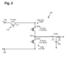
- FIG. 2 shows exemplary half bridge circuit 200.
- Figure 2 is another example of utilizing a switch circuit including a combination of at least two depletion mode III-Nitride FETs together with an enhancement mode group IV enable switch.
- Half bridge circuit 200 includes high side switch 220a coupled to low side switch 220b at switch node 232. As shown in Figure 2 , high side switch 220a and low side switch 220b are coupled between high voltage rail 206 and grounded rail 208 of half bridge circuit 200.
- load 218 coupled to switch node 232 through output inductor 234, and capacitor 238. It is noted that although load 218 is represented by a resistive component in Figure 2 , more generally, load 218 may either be predominantly one of or a combination of inductance, resistance, and capacitance.
- Figure 2 provides another example of utilizing an enhancement mode enable switch on the high side rail. That is to say, enhancement mode FET 210 is connected in series between input voltage V+ to high voltage rail 206 and high side switch 220a. As such, drain 214 of FET 210 may be coupled to source 222a of depletion mode III-Nitride HEMT 220a and source 222b of depletion mode III-Nitride HEMT 220b may be coupled to switch node 232.
- enhancement mode enable switch 210 may be implemented as a LV, MV, or HV enhancement mode group IV FET as defined above.
- the enhancement mode group IV enable switch with one or more depletion mode III-Nitride power transistors may be advantageous or desirable to monolithically integrate the enhancement mode group IV enable switch with one or more depletion mode III-Nitride power transistors.
- Such integration may be achieved, for example, using recent advances in high power III-Nitride HEMT development on silicon substrates, as well as advances in the integration of silicon based devices with III-Nitride based devices.
- U.S. Patent Number 7,915,645 entitled “Monolithic Vertically Integrated Composite Group III-V And Group IV Semiconductor Device and Method For Fabricating Same", and issued on March 29, 2011; U.S.
- Patent Application Number 13/020,243 entitled “Efficient High Voltage Switching Circuits And Monolithic Integration of Same", and filed on February 3, 2011
- U.S. Patent Application Number 12/174,329 entitled “III-Nitride Device", and filed on July 16, 2008
- U.S. Patent Application Number 13/544,267 entitled “Composite Semiconductor Device with Integrated Diode”, and filed on July 9, 2012.
- FIG. 3 shows a cross-sectional view of a monolithically integrated power device, also referred to herein as a "monolithically integrated component," including two or more depletion mode III-Nitride transistors and an enhancement mode group IV IGBT enable switch, according to one implementation.
- Monolithically integrated component 300 includes enhancement mode group IV IGBT switch 310 and depletion mode III-Nitride transistors 330a and 330b.
- Enhancement mode group IV IGBT 310 and depletion mode III-Nitride transistors 330a and 330b correspond in general to enhancement mode IGBT 110 and depletion mode III-Nitride HEMTs 120a and 120b, respectively, in Figure 1 , and may share any of the characteristics attributed to those corresponding features above.
- depletion mode III-Nitride transistors 330a and 330b may be implemented as III-Nitride HEMTs, while enhancement mode group IV switch 310 may take the form of a silicon IGBT configured as an enhancement mode enable switch for depletion mode III-Nitride transistors 330a and 330b (hereinafter "III-Nitride HEMTs 330a and 330b").
- enhancement mode group IV IGBT 310 (hereinafter “silicon IGBT 310") is formed in the silicon substrate supporting III-Nitride HEMTs 330a and 330b.
- Silicon IGBT 310 includes IGBT body layer 318, drift layer 320 situated over IGBT body layer 318, collector layer 312 situated over drift layer 320, and may include optional silicon interlayers 324 situated over collector layer 312.
- silicon IGBT 310 may also include field stop layer 322 situated between drift layer 320 and collector layer 312.
- silicon IGBT 310 includes emitter regions 314 and gate 316 formed in IGBT body layer 318. It is noted that in other implementations, there may be other layers and/or regions formed within a group IV IGBT enable switch corresponding to silicon IGBT 310 that are not shown in Figure 3 .
- III-Nitride HEMTs 330a and 330b include optional amorphous silicon nitride (SiN) layer 338, and nucleation layer or layers 340, which may be aluminum nitride (AlN) nucleation layer(s) 340, for example, formed over silicon IGBT 310.
- III-Nitride HEMTs 330a and 330b also include transition layer or layers 342 situated over collector layer 312.
- optional silicon interlayers 324 and/or optional amorphous SiN layer 338 and/or nucleation layer(s) 340 and/or transition layer(s) 342 may be situated between collector layer 312 of silicon IGBT 310 and III-Nitride buffer layer 344.
- III-Nitride HEMTs 330a and 330b also include buffer layer 344 situated over transition layer(s) 342, channel layer 346 situated over buffer layer 344, and barrier layer or layers 348 situated over channel layer 346.
- Transition layer(s) 342 may include compositionally graded III-Nitride layers, III-Nitride superlattice structures, low temperature AlN interlayers, stress modulation layers or a combination of any above.
- Transition layer(s) 342, buffer layer 344, channel layer 346, and barrier layer(s) 348 may be formed so as to have any suitable III-Nitride semiconductor composition.
- transition layer(s) 342, buffer layer 344, channel layer 346, and barrier layer(s) 348 may be III-Nitride layers, such as GaN based layers, for example.
- barrier layer(s) 348 is/are formed over channel layer 346 having a smaller bandgap than barrier layer(s) 348, such that 2DEG 347 is generated at or near their interface.
- barrier layer(s) 348 there may also be other interlayers, for example, one or more AlN interlayers, formed between barrier layer(s) 348 and channel layer 346, and/or III-N based cap layers formed on barrier layer(s) 348.
- III-Nitride HEMT 330a and 330b include respective source and drain electrodes.
- III-Nitride HEMT 330a includes source 334a, drain 332a, and gate 336a, which may be a Schottky gate (as shown) or an insulated gate using a gate dielectric layer under the gate (not shown in Figure 3 ), for example, situated over barrier layer(s) 348.
- III-Nitride HEMT 330b includes source 334b, drain 332b, as well as gate 336b. Additional device layers may also be formed over the III-Nitride device structure including additional dielectric layers, source, gate and/or drain field plates, and additional metallization layers.
- III-Nitride HEMTs 330a and 330b are electrically isolated from each other by isolation feature 350 (e.g., isolation implant or isolation etch, for example).
- amorphous SiN based layer 338 may be situated between nucleation layer(s) 340 and optional silicon interlayers 324 or the silicon substrate.
- An example of such a structure is disclosed in U.S. Patent Number 7,352,015 , entitled “Gallium Nitride Materials and Methods Associated With the Same", issued on April 1, 2008. The entire disclosure in this patent is hereby incorporated fully by reference into the present application.
- amorphous SiN layer 338, nucleation layer(s) 340, transition layer(s) 342, and buffer layer 344 are formed above the silicon layer serving as IGBT collector layer 312.
- amorphous SiN layer 338, and/or nucleation layer(s) 340, transition layer(s) 342, and buffer layer 344 may be formed directly on IGBT collector layer 312, or may be formed on silicon interlayers 324 formed between III-Nitride HEMT 330a and 330b layers and collector layer 312. Silicon interlayers 324 may include N+ layers, and/or oxide/insulating layer(s), for example.
- IGBT collector layer 312 is formed on or over drift layer 320.
- the thickness of drift layer 320 is selected such that silicon IGBT 310 can stand off the supply voltage that III-Nitride HEMT(s) 330 and/or 330b is designed to withstand, which may be a voltage between approximately 300 V and approximately 2000 V, for example.
- IGBT body layer 318 Underlying drift layer 320 is IGBT body layer 318.
- emitter regions 314 are formed within IGBT body layer 318, which is controlled using IGBT gate 316.
- IGBT gate 316 may be formed vertically, such as in a trench, as shown in Figure 3 , or may be formed as a planar gate structure (planar gate not shown in Figure 3 ). Because silicon IGBT 310 is configured to operate as a DC enable switch for III-Nitride HEMT(s) 330a and/or 330b, the design of silicon IGBT 310 may be optimized to provide a substantially minimal on-resistance, at the acceptable cost of slower switching.
- silicon IGBT 310 when operating as a DC enable switch, silicon IGBT 310 will typically be switched at frequencies of less than approximately 1.0 Hz. As a result, it is reiterated that high frequency operation is not required for the present implementations of a group IV enable switch corresponding to silicon IGBT 310. It is also noted that although the design of enable switch 310 is shown as an IGBT, in certain implementations, the design of the enable switch may take the form of a silicon or other group IV based FET, including a multiple Reduced Surface Field (RESURF), highly compensated, or super-junction based FET.
- RESURF Reduced Surface Field
- III-Nitride HEMT(s) 330a and/or 330b and silicon IGBT 310 may be electrically connected in series using interconnect vias, or through substrate vias or plugs, or using wire bonding techniques and packaging options know in the art. More specifically, it may be advantageous or desirable to form the electrical connections shown in figures 1 and 2 through one or more bond wires, such as gold (Au) or copper (Cu) bond wires, for example.
- one or more bond wires may be replaced by conductive ribbons, conductive metal clips, or other connectors formed of conductive materials such as Al, Au, Cu, and/or other metals or composite materials.
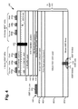
- FIGS 4 and 5 show two alternative examples of monolithically integrated two or more depletion mode III-Nitride HEMTs and an enhancement mode group IV IGBT.
- monolithically integrated component 400 includes enhancement mode group IV IGBT 410 and depletion mode III-Nitride transistors 430a and 430b.
- Enhancement mode group IV IGBT 410 and depletion mode III-Nitride transistors 430a and 430b correspond in general to enhancement mode IGBT 110 and depletion mode III-Nitride FETs 120a and 120b, respectively, in Figure 1 , and may share any of the characteristics attributed to those corresponding features above.
- depletion mode III-Nitride transistors 430a and 430b may be implemented as III-Nitride HEMTs
- enhancement mode group IV IGBT switch 410 may take the form of a silicon IGBT configured as an enable switch for depletion mode III-Nitride transistor(s) 430a and/or 430b (hereinafter "III-Nitride HEMTs 430a and 430b").
- enhancement mode group IV IGBT 410 (hereinafter “silicon IGBT 410") is formed in the silicon substrate supporting III-Nitride HEMTs 430a and 430b.
- Silicon IGBT 410 includes IGBT body layer 418, drift layer 420 situated over IGBT body layer 418, and collector layer 412 situated over drift layer 420.
- silicon IGBT 410 may also include field stop layer 422 situated between drift layer 420 and collector layer 412.
- silicon IGBT 410 includes emitter regions 414 and gate 416 formed in IGBT body layer 418.
- silicon IGBT 410 may include silicon interlayers situated on or over collector layer 412.
- III-Nitride HEMTs 430a and 430b include optional amorphous silicon nitride (SiN) layer 438, and nucleation layer or layers 440, which may be aluminum nitride (AlN) nucleation layer(s) 440, for example, formed over silicon IGBT 410.
- III-Nitride HEMTs 430a and 430b may also transition layers 442 situated over collector layer 412.
- optional amorphous SiN layer 438 and/or nucleation layer(s) 440 and/or transition layer(s) 442 may be situated between collector layer 412 of silicon IGBT 410 and buffer layer 444.
- III-Nitride HEMTs 430a and 430b also include buffer layer 444 situated over transition layer(s) 442, channel layer 446 situated over buffer layer 444, and barrier layer or layers 448 situated over channel layer 446.
- collector layer 412 may be substantially coplanar with a top surface of collector layer 412 having exposed portion 445. That is to say, collector electrode 450 of silicon IGBT 410 is situated on the top side of monolithically integrated component 400, opposite IGBT emitter 414 and IGBT gate 416 regions situated on the bottom side of monolithically integrated component 400.
- Transition layer(s) 442, buffer layer 444, channel layer 446, and barrier layer(s) 448 may be formed so as to have any suitable III-Nitride semiconductor composition.
- transition layer(s) 442, buffer layer 444, channel layer 446, and barrier layer(s) 448 may be III-Nitride layers, such as GaN based layers, for example.
- barrier layer(s) 448 is/are formed over channel layer 446 having a smaller bandgap than barrier layer(s) 448, such that 2DEG 447 is generated at or near their interface.
- interlayers there may also be other interlayers, for example, one or more AlN interlayers, formed between barrier layer(s) 448 and channel layer 446, and/or III-Nitride based capping layers formed on barrier layer(s) 448.
- interlayers for example, one or more AlN interlayers, formed between barrier layer(s) 448 and channel layer 446, and/or III-Nitride based capping layers formed on barrier layer(s) 448.
- III-Nitride HEMTs 430a and 430b include respective source and drain electrodes.
- III-Nitride HEMT 430a includes source 434a, drain 432a, and gate 436a, which may be a Schottky gate (as shown) or may be an insulated gate using a gate dielectric (not shown in Figure 4 ), for example, situated over barrier layer(s) 448. That is to say, source electrode 434a, drain electrode 432a, and gate 436a of III-Nitride HEMT 430a are formed on the top side of monolithically integrated component 400, opposite the bottom side on which electrodes for IGBT gate 416 and emitter regions 414 are formed.
- III-Nitride HEMT 430b includes source 434b, drain 434b, and gate 436b. Additional device layers may also be formed over the III-Nitride device structure including additional dielectric layers, source, gate, and/or drain field plates, and additional metallization layers. III-Nitride HEMTs 430a and 430b are electrically isolated from each other by isolation feature 450 (e.g., isolation implant or isolation etch, for example).
- isolation feature 450 e.g., isolation implant or isolation etch, for example.
- channel layer 446 and barrier layer(s) 448 is typically formed over buffer layer 444, as well as over underlying compositionally graded transition layer(s) 442, which may include additional stress reduction layers, superlattice layers, low temperature AlN interlayers or stress modulation layers not explicitly shown in Figure 4 .
- amorphous SiN based layer 438 may be situated between nucleation layer(s) 440 and the aforementioned optional silicon interlayers or the silicon substrate.
- amorphous SiN layer 438, nucleation layer(s) 440, transition layer(s) 442, and buffer layer 444 are formed over the silicon layer serving as IGBT collector layer 412.
- amorphous SiN layer 438, and/or nucleation layer(s) 440, transition layer(s) 442, and buffer layer 444 may be formed directly on IGBT collector layer 412, or may be formed on silicon interlayers formed between the III-Nitride HEMT layers and collector layer 412 (silicon interlayers not shown in Figure 4 ).
- IGBT collector layer 412 is formed on or over drift layer 420.
- drift layer 420 is selected such that silicon IGBT 410 can stand off the supply voltage that III-Nitride HEMT(s) 430a and/or 430b is designed to withstand, which may be a voltage between approximately 300 V and approximately 2000 V, for example.
- IGBT body layer 418 Underlying drift layer 420 is IGBT body layer 418. Typically, emitter regions 414 are formed within IGBT body layer 418, which is controlled using IGBT gate 416.
- IGBT gate 416 may be formed vertically, such as in a trench, as shown in Figure 4 , or may be formed as a planar gate structure (planar gate not shown in Figure 4 ). Because silicon IGBT 410 is configured to operate as a DC enable switch for III-Nitride HEMT(s) 430a and/or 430b, the design of silicon IGBT 410 may be optimized to provide a substantially minimal on-resistance, at the acceptable cost of slower switching, as discussed by reference to Figure 3 above.
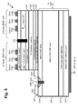
- Figure 5 is yet another example of monolithically integrating two or more depletion mode III-Nitride HEMTs and an enhancement mode silicon IGBT enable switch.
- Figure 5 shows a cross-sectional view of an exemplary monolithically integrated power device including two or more III-Nitride transistors and a group IV IGBT enable switch having a top side gate.
- Monolithically integrated component 500 includes enhancement mode group IV IGBT 510 and depletion mode III-Nitride transistors 530a and 530b.
- Enhancement mode group IV IGBT 510 and depletion mode III-Nitride transistors 530a and 530b correspond in general to enhancement mode IGBT 110 and depletion mode III-Nitride FETs 120a and 120b, respectively, in Figure 1 , and may share any of the characteristics attributed to those corresponding features above.
- depletion mode III-Nitride transistors 530a and 530b may be implemented as depletion mode III-Nitride HEMTs
- enhancement mode group IV IGBT 510 may take the form of a silicon IGBT configured as an enhancement mode enable switch for depletion mode III-Nitride depletion mode transistors 530a and 530b (hereinafter "III-Nitride HEMT 530a and 530b").
- enhancement mode group IV IGBT 510 (hereinafter “silicon IGBT 510") is formed in the silicon substrate supporting III-Nitride HEMTs 530a and 530b.
- Silicon IGBT 510 includes collector layer 512 coupled to collector electrode 550 situated on the bottom side or backside of monolithically integrated component 500, drift layer 520 situated over collector layer 512, and IGBT body layer 518 situated over drift layer 520.
- emitter regions 514 and gate 516 of silicon IGBT 510 are situated in exposed portion 528 of IGBT body layer 518. That is to say, emitter regions 514 and gate 516 of silicon IGBT 510 are situated on the top side of monolithically integrated component 500, opposite collector electrode 550 situated on the bottom side of monolithically integrated component 500.
- silicon IGBT 510 may also include optional field stop layer 522 situated between drift layer 520 and collector layer 512. It is noted that although collector layer 512, optional field stop layer 522, drift layer 520, and IGBT body layer 518 are shown as silicon layers in Figure 5 , more generally, collector layer 512, field stop layer 522, drift layer 520, and IGBT body layer 518 may be implemented as any group IV semiconductor layers suitable for use in a group IV IGBT corresponding to silicon IGBT 510.
- monolithically integrated component 500 includes III-Nitride HEMTs 530a and 530b situated over IGBT body layer 518 adjacent exposed portion 528.
- III-Nitride HEMTs 530a and 530b may include respective source, drain and gate electrodes.
- III-Nitride HEMT 530a includes source 534a, drain 532a, and gate 536a, which may be a Schottky gate (as shown) or insulated gate using a gate dielectric layer (not shown in Figure 5 ), for example, formed thereon, over barrier layer(s) 548.
- III-Nitride HEMT 530a are formed on the top side or front side of monolithically integrated component 500, opposite the bottom side or backside side on which collector electrode 550 of silicon IGBT 510 is situated.
- III-Nitride HEMT 530b includes source 534b, drain 532b and gate 536b. Additional device layers may also be formed over the III-Nitride device structure including additional dielectric layers, source, gate and/or drain field plates, and additional metallization layers.
- III-Nitride HEMTs 530a and 530b are electrically isolated from each other by isolation feature 550 (e.g., isolation implant or isolation etch, for example).
- III-Nitride HEMTs 530a and 530b include optional amorphous silicon nitride (SiN) based layer 538, and nucleation layer or layers 540, which may be aluminum nitride (AlN) nucleation layer(s) 540, for example, formed over IGBT body layer 518.
- III-Nitride HEMTs 530a and 530b also includes transition layer or layers 542 situated over IGBT body layer 518, buffer layer 544 situated over transition layer(s) 542, channel layer 546 situated over buffer layer 544, and barrier layer or layers 548 situated over channel layer 546.
- optional amorphous SiN layer 538 and/or nucleation layer(s) 540 and/or transition layer(s) 542 may be situated between IGBT body layer 518 and buffer layer 544 of III-Nitride HEMTs 530a and 530b.
- Transition layer(s) 542, buffer layer 544, channel layer 546, and barrier layer(s) 548 may be formed so as to have any suitable III-Nitride semiconductor composition.
- transition layer(s) 542, buffer layer 544, channel layer 546, and barrier layer(s) 548 may be III-Nitride layers, such as GaN based layers, for example.
- barrier layer(s) 548 is/are formed over channel layer 546 having a smaller bandgap than barrier layer(s) 548, such that 2DEG 547 is generated at or near their interface.
- interlayers there may also be other interlayers, for example, one or more AlN interlayers, formed between barrier layer(s) 548 and channel layer 546, and/or III-Nitride based capping layers formed on barrier layer(s) 548.
- interlayers for example, one or more AlN interlayers, formed between barrier layer(s) 548 and channel layer 546, and/or III-Nitride based capping layers formed on barrier layer(s) 548.
- channel layer 546 and barrier layer(s) 548 is typically formed over buffer layer 544, as well as over underlying compositionally graded transition layer(s) 542, which may include additional stress reduction layers, superlattice layers, low temperature AlN interlayers or stress reduction module layers not explicitly shown in Figure 5 .
- amorphous SiN based layer 538 may be situated between nucleation layer(s) 540 and the silicon substrate in which silicon IGBT 510 is formed as discussed above be reference to Figure 3 .
- silicon IGBT 510 may include silicon or other group IV interlayers situated between IGBT body layer 518 and the III-Nitride HEMT layers.
- amorphous SiN layer 538, and/or nucleation layer(s) 540, transition layer(s) 542, and buffer layer 544 may be formed directly on IGBT body layer 518, or may be formed on silicon or other group IV interlayers formed between III-Nitride HEMT layers and collector layer 512 (silicon or other group IV interlayers not shown in Figure 5 ).
- IGBT body layer 518 is formed on or over drift layer 520.
- drift layer 520 is selected such that silicon IGBT 510 can stand off the supply voltage that III-Nitride HEMT 530a and/or 530b is designed to withstand, which may be a voltage between approximately 300 V and approximately 2000 V, for example.
- IGBT gate 516 may be formed vertically, such as in a trench, as shown in Figure 5 , or may be formed as a planar gate structure (planar gate not shown in Figure 5 ).
- silicon IGBT 510 is configured to operate as a DC enable switch for III-Nitride HEMT(s) 530a and/or 530b
- the design of silicon IGBT 510 may be optimized to provide a substantially minimal on-resistance, at the acceptable cost of slower switching.
- silicon IGBT 510 when operating as a DC enable switch, will typically be switched at frequencies of less than approximately 1.0 Hz. As a result, it is reiterated that high frequency operation is not required for the present implementations of a group IV enable switch corresponding to silicon IGBT 510.
- the present application discloses various implementations of a monolithically integrated power device including two or more III-Nitride transistors and a group IV switch.
- the III-Nitride transistors may be depletion mode III-Nitride transistors
- the group IV switch may be implemented as an enhancement mode silicon IGBT enable switch, or as an enhancement mode silicon FET enable switch, in the conduction path of one or more of the depletion mode III-Nitride transistors, in order to make or break the conduction path to or from at least one depletion mode III-Nitride transistor.
- the monolithically integrated power devices disclosed herein enable prevention of damage to a load driven by a power conversion circuit including such power devices due to premature power up (i.e., bias is applied to the switch terminals) of the circuitry prior to biasing of at least one of the depletion mode III-Nitride transistors to hold it in the high resistive of off-state (OFF).
- the enhancement mode group IV enable switch may be used to disconnect at least one depletion mode III-Nitride transistor from the bus or high voltage rail of the power conversion circuit to provide protection for the depletion mode III-Nitride transistors and the load.
Landscapes
- Engineering & Computer Science (AREA)
- Power Engineering (AREA)
- Junction Field-Effect Transistors (AREA)
- Dc-Dc Converters (AREA)
- Semiconductor Integrated Circuits (AREA)
- Metal-Oxide And Bipolar Metal-Oxide Semiconductor Integrated Circuits (AREA)
Applications Claiming Priority (2)
| Application Number | Priority Date | Filing Date | Title |
|---|---|---|---|
| US201361845913P | 2013-07-12 | 2013-07-12 | |
| US14/327,495 US9184243B2 (en) | 2013-07-12 | 2014-07-09 | Monolithic composite III-nitride transistor with high voltage group IV enable switch |
Publications (1)
| Publication Number | Publication Date |
|---|---|
| EP2824700A1 true EP2824700A1 (fr) | 2015-01-14 |
Family
ID=51162573
Family Applications (1)
| Application Number | Title | Priority Date | Filing Date |
|---|---|---|---|
| EP20140176508 Withdrawn EP2824700A1 (fr) | 2013-07-12 | 2014-07-10 | Transistor à base de nitrure III composite monolithique avec commutateur de validation haute tension du groupe IV |
Country Status (3)
| Country | Link |
|---|---|
| US (1) | US9184243B2 (fr) |
| EP (1) | EP2824700A1 (fr) |
| JP (1) | JP6012671B2 (fr) |
Cited By (5)
| Publication number | Priority date | Publication date | Assignee | Title |
|---|---|---|---|---|
| CN106603052A (zh) * | 2015-10-15 | 2017-04-26 | 英飞凌科技奥地利有限公司 | 双向常闭型器件和电路 |
| US10447159B2 (en) | 2015-05-29 | 2019-10-15 | Wupatec | DC-DC converter block, DC-DC converter comprising same and associated system envelope tracking system |
| EP3866189A1 (fr) * | 2020-02-14 | 2021-08-18 | Epinovatech AB | Module mmic frontal |
| TWI783830B (zh) * | 2021-12-20 | 2022-11-11 | 世界先進積體電路股份有限公司 | 半導體裝置 |
| US12310105B2 (en) | 2022-03-02 | 2025-05-20 | Vanguard International Semiconductor Corporation | Semiconductor device including high electron mobility transistors with an improved backside electrode being applied in a half-bridge circuit |
Families Citing this family (17)
| Publication number | Priority date | Publication date | Assignee | Title |
|---|---|---|---|---|
| US9502401B2 (en) * | 2013-08-16 | 2016-11-22 | Infineon Technologies Austria Ag | Integrated circuit with first and second switching devices, half bridge circuit and method of manufacturing |
| US9257424B2 (en) * | 2013-11-08 | 2016-02-09 | Infineon Technologies Austria Ag | Semiconductor device |
| US20160293597A1 (en) * | 2015-04-06 | 2016-10-06 | Infineon Technologies Austria Ag | Integrated Semiconductor Device |
| US9660062B2 (en) * | 2015-04-30 | 2017-05-23 | Semiconductor Components Industries, Llc | Bidirectional HEMT and an electronic package including the bidirectional HEMT |
| US9911712B2 (en) | 2015-10-26 | 2018-03-06 | Semiconductor Components Industries, Llc | Clip and related methods |
| US9627275B1 (en) | 2015-10-30 | 2017-04-18 | Taiwan Semiconductor Manufacturing Company Ltd. | Hybrid semiconductor structure on a common substrate |
| US10505032B2 (en) | 2015-10-30 | 2019-12-10 | The Hong Kong University Of Science And Technology | Semiconductor device with III-nitride channel region and silicon carbide drift region |
| US10217827B2 (en) * | 2016-05-11 | 2019-02-26 | Rfhic Corporation | High electron mobility transistor (HEMT) |
| WO2019066872A1 (fr) * | 2017-09-28 | 2019-04-04 | Intel Corporation | Intégration monolithique d'un transistor à film mince sur un transistor complémentaire |
| JP7000187B2 (ja) * | 2018-02-08 | 2022-01-19 | エイブリック株式会社 | 基準電圧回路及び半導体装置 |
| JP7316757B2 (ja) | 2018-02-23 | 2023-07-28 | ローム株式会社 | 半導体装置 |
| CN109742143A (zh) * | 2018-12-29 | 2019-05-10 | 苏州汉骅半导体有限公司 | 集成增强型和耗尽型的hemt及其制造方法 |
| WO2020191357A1 (fr) * | 2019-03-21 | 2020-09-24 | Transphorm Technology, Inc. | Conception intégrée pour dispositifs au nitrure iii |
| CN112909077B (zh) * | 2021-02-07 | 2022-03-29 | 电子科技大学 | 一种双异质结极化增强的准纵向GaN HEMT器件 |
| US12520548B2 (en) | 2021-10-27 | 2026-01-06 | Industrial Technology Research Institute | Semiconductor substrate with balanced stress |
| TWI785864B (zh) | 2021-10-27 | 2022-12-01 | 財團法人工業技術研究院 | 半導體基板以及電晶體 |
| CN119677121B (zh) * | 2024-11-27 | 2026-04-07 | 西安电子科技大学 | 一种具有沟槽栅结构的绝缘栅双极晶体管及其制备方法 |
Citations (12)
| Publication number | Priority date | Publication date | Assignee | Title |
|---|---|---|---|---|
| US6211549B1 (en) * | 1997-09-17 | 2001-04-03 | Kabushiki Kaisha Toshiba | High breakdown voltage semiconductor device including first and second semiconductor elements |
| US6611002B2 (en) | 2001-02-23 | 2003-08-26 | Nitronex Corporation | Gallium nitride material devices and methods including backside vias |
| EP1643561A2 (fr) * | 2004-09-30 | 2006-04-05 | The Furukawa Electric Co., Ltd. | Circuit semiconducteur intégré à base de GaN |
| US7352015B2 (en) | 2004-06-28 | 2008-04-01 | Nitronex Corporation | Gallium nitride materials and methods associated with the same |
| US7566913B2 (en) | 2005-12-02 | 2009-07-28 | Nitronex Corporation | Gallium nitride material devices including conductive regions and methods associated with the same |
| EP2256799A2 (fr) * | 2009-05-28 | 2010-12-01 | International Rectifier Corporation | Dispositif de semi-conducteurs de groupe III-V et de groupe IV composite intégré verticalement monolithique, et son procédé de fabrication |
| US7902809B2 (en) | 2006-11-28 | 2011-03-08 | International Rectifier Corporation | DC/DC converter including a depletion mode power switch |
| US20110080156A1 (en) * | 2006-11-28 | 2011-04-07 | International Rectifier Corporation | DC/DC converter with depletion-mode III-nitride switches |
| US20120235209A1 (en) * | 2011-03-18 | 2012-09-20 | International Rectifier Corporation | High Voltage Rectifier and Switching Circuits |
| EP2546987A2 (fr) * | 2011-07-11 | 2013-01-16 | International Rectifier Corporation | Commutateur composite imbriqué |
| US20130087803A1 (en) * | 2011-10-06 | 2013-04-11 | Epowersoft, Inc. | Monolithically integrated hemt and schottky diode |
| US20130146888A1 (en) * | 2011-12-07 | 2013-06-13 | Samsung Electro-Mechanics Co., Ltd. | Monolithic semiconductor device and method for manufacturing the same |
Family Cites Families (6)
| Publication number | Priority date | Publication date | Assignee | Title |
|---|---|---|---|---|
| WO2008086001A2 (fr) | 2007-01-10 | 2008-07-17 | International Rectifier Corporation | Mise en forme de zone active pour dispositif au nitrure iii et procédé de fabrication |
| US20090050939A1 (en) | 2007-07-17 | 2009-02-26 | Briere Michael A | Iii-nitride device |
| US8242510B2 (en) * | 2010-01-28 | 2012-08-14 | Intersil Americas Inc. | Monolithic integration of gallium nitride and silicon devices and circuits, structure and method |
| US9219058B2 (en) * | 2010-03-01 | 2015-12-22 | Infineon Technologies Americas Corp. | Efficient high voltage switching circuits and monolithic integration of same |
| US9087812B2 (en) | 2011-07-15 | 2015-07-21 | International Rectifier Corporation | Composite semiconductor device with integrated diode |
| US9349715B2 (en) | 2013-06-21 | 2016-05-24 | Infineon Technologies Americas Corp. | Depletion mode group III-V transistor with high voltage group IV enable switch |
-
2014
- 2014-07-09 US US14/327,495 patent/US9184243B2/en active Active
- 2014-07-10 JP JP2014142500A patent/JP6012671B2/ja not_active Expired - Fee Related
- 2014-07-10 EP EP20140176508 patent/EP2824700A1/fr not_active Withdrawn
Patent Citations (13)
| Publication number | Priority date | Publication date | Assignee | Title |
|---|---|---|---|---|
| US6211549B1 (en) * | 1997-09-17 | 2001-04-03 | Kabushiki Kaisha Toshiba | High breakdown voltage semiconductor device including first and second semiconductor elements |
| US6611002B2 (en) | 2001-02-23 | 2003-08-26 | Nitronex Corporation | Gallium nitride material devices and methods including backside vias |
| US7352015B2 (en) | 2004-06-28 | 2008-04-01 | Nitronex Corporation | Gallium nitride materials and methods associated with the same |
| EP1643561A2 (fr) * | 2004-09-30 | 2006-04-05 | The Furukawa Electric Co., Ltd. | Circuit semiconducteur intégré à base de GaN |
| US7566913B2 (en) | 2005-12-02 | 2009-07-28 | Nitronex Corporation | Gallium nitride material devices including conductive regions and methods associated with the same |
| US7902809B2 (en) | 2006-11-28 | 2011-03-08 | International Rectifier Corporation | DC/DC converter including a depletion mode power switch |
| US20110080156A1 (en) * | 2006-11-28 | 2011-04-07 | International Rectifier Corporation | DC/DC converter with depletion-mode III-nitride switches |
| EP2256799A2 (fr) * | 2009-05-28 | 2010-12-01 | International Rectifier Corporation | Dispositif de semi-conducteurs de groupe III-V et de groupe IV composite intégré verticalement monolithique, et son procédé de fabrication |
| US7915645B2 (en) | 2009-05-28 | 2011-03-29 | International Rectifier Corporation | Monolithic vertically integrated composite group III-V and group IV semiconductor device and method for fabricating same |
| US20120235209A1 (en) * | 2011-03-18 | 2012-09-20 | International Rectifier Corporation | High Voltage Rectifier and Switching Circuits |
| EP2546987A2 (fr) * | 2011-07-11 | 2013-01-16 | International Rectifier Corporation | Commutateur composite imbriqué |
| US20130087803A1 (en) * | 2011-10-06 | 2013-04-11 | Epowersoft, Inc. | Monolithically integrated hemt and schottky diode |
| US20130146888A1 (en) * | 2011-12-07 | 2013-06-13 | Samsung Electro-Mechanics Co., Ltd. | Monolithic semiconductor device and method for manufacturing the same |
Non-Patent Citations (1)
| Title |
|---|
| CHYURLIA P N ET AL: "Monolithic integration of AlGaN/GaN HFET with MOS on silicon <111> substrates", ELECTRONIC LETTERS, THE INSTITUTION OF ENGINEERING AND TECHNOLOGY, vol. 46, no. 3, 4 February 2010 (2010-02-04), pages 240 - 242, XP006034757, ISSN: 1350-911X, DOI: 10.1049/EL:20103167 * |
Cited By (7)
| Publication number | Priority date | Publication date | Assignee | Title |
|---|---|---|---|---|
| US10447159B2 (en) | 2015-05-29 | 2019-10-15 | Wupatec | DC-DC converter block, DC-DC converter comprising same and associated system envelope tracking system |
| CN106603052A (zh) * | 2015-10-15 | 2017-04-26 | 英飞凌科技奥地利有限公司 | 双向常闭型器件和电路 |
| EP3866189A1 (fr) * | 2020-02-14 | 2021-08-18 | Epinovatech AB | Module mmic frontal |
| WO2021160728A1 (fr) * | 2020-02-14 | 2021-08-19 | Epinovatech Ab | Module d'extrémité avant de circuit intégré hyperfréquence monolithique |
| AU2021220276B2 (en) * | 2020-02-14 | 2024-05-02 | Epinovatech Ab | A monolithic microwave integrated circuit front-end module |
| TWI783830B (zh) * | 2021-12-20 | 2022-11-11 | 世界先進積體電路股份有限公司 | 半導體裝置 |
| US12310105B2 (en) | 2022-03-02 | 2025-05-20 | Vanguard International Semiconductor Corporation | Semiconductor device including high electron mobility transistors with an improved backside electrode being applied in a half-bridge circuit |
Also Published As
| Publication number | Publication date |
|---|---|
| US9184243B2 (en) | 2015-11-10 |
| JP6012671B2 (ja) | 2016-10-25 |
| JP2015043414A (ja) | 2015-03-05 |
| US20150014740A1 (en) | 2015-01-15 |
Similar Documents
| Publication | Publication Date | Title |
|---|---|---|
| US9184243B2 (en) | Monolithic composite III-nitride transistor with high voltage group IV enable switch | |
| US11217687B2 (en) | Power semiconductor device with an auxiliary gate structure | |
| TWI499058B (zh) | 氮化鎵二極體及積體組件 | |
| US9406674B2 (en) | Integrated III-nitride D-mode HFET with cascoded pair half bridge | |
| US9349715B2 (en) | Depletion mode group III-V transistor with high voltage group IV enable switch | |
| US9818686B2 (en) | Semiconductor modules and methods of forming the same | |
| US9041067B2 (en) | Integrated half-bridge circuit with low side and high side composite switches | |
| US8987833B2 (en) | Stacked composite device including a group III-V transistor and a group IV lateral transistor | |
| US8981380B2 (en) | Monolithic integration of silicon and group III-V devices | |
| EP2639829B1 (fr) | Commutateur composite du groupe III-V et du groupe IV | |
| EP2884536A1 (fr) | Convertisseur de tension du groupe III-V à décalage de niveau intégré de façon monolithique, circuit de commande côté tension haute et commutateur de puissance côté tension haute | |
| EP2511952A1 (fr) | Dispositif composite empilé comprenant un transistor du groupe III-V et un transistor vertical du groupe IV | |
| EP2363885A2 (fr) | Circuits de commutation efficace haute tension et intégration monolithique correspondante | |
| JP2012212875A (ja) | 低電圧デバイス保護付き高電圧複合半導体デバイス | |
| WO2013066967A1 (fr) | Jfet vertical et diode schottky intégrés de manière monolithique | |
| EP2881989A1 (fr) | Dispositif de puissance composite avec pince de protection contre les décharges électrostatiques | |
| CN111213241B (zh) | 半导体器件、半导体设备及其制造方法 | |
| EP2511954A1 (fr) | Dispositif composite empilé comprenant un transistor du groupe III-V et diode de groupe IV | |
| US20130175542A1 (en) | Group III-V and Group IV Composite Diode | |
| EP2639832A2 (fr) | Diode composite du groupe III-V et du groupe IV |
Legal Events
| Date | Code | Title | Description |
|---|---|---|---|
| 17P | Request for examination filed |
Effective date: 20140710 |
|
| AK | Designated contracting states |
Kind code of ref document: A1 Designated state(s): AL AT BE BG CH CY CZ DE DK EE ES FI FR GB GR HR HU IE IS IT LI LT LU LV MC MK MT NL NO PL PT RO RS SE SI SK SM TR |
|
| AX | Request for extension of the european patent |
Extension state: BA ME |
|
| PUAI | Public reference made under article 153(3) epc to a published international application that has entered the european phase |
Free format text: ORIGINAL CODE: 0009012 |
|
| RIN1 | Information on inventor provided before grant (corrected) |
Inventor name: BRIERE, MICHAEL A. |
|
| R17P | Request for examination filed (corrected) |
Effective date: 20150709 |
|
| RBV | Designated contracting states (corrected) |
Designated state(s): AL AT BE BG CH CY CZ DE DK EE ES FI FR GB GR HR HU IE IS IT LI LT LU LV MC MK MT NL NO PL PT RO RS SE SI SK SM TR |
|
| 17Q | First examination report despatched |
Effective date: 20170411 |
|
| RAP1 | Party data changed (applicant data changed or rights of an application transferred) |
Owner name: INFINEON TECHNOLOGIES AMERICAS CORP. |
|
| STAA | Information on the status of an ep patent application or granted ep patent |
Free format text: STATUS: THE APPLICATION IS DEEMED TO BE WITHDRAWN |
|
| 18D | Application deemed to be withdrawn |
Effective date: 20190326 |