EP2824711A2 - Transistors verticaux disposant de couches de barrières de courant au nitrure de gallium de type P et leurs procédés de fabrication - Google Patents
Transistors verticaux disposant de couches de barrières de courant au nitrure de gallium de type P et leurs procédés de fabrication Download PDFInfo
- Publication number
- EP2824711A2 EP2824711A2 EP14176590.9A EP14176590A EP2824711A2 EP 2824711 A2 EP2824711 A2 EP 2824711A2 EP 14176590 A EP14176590 A EP 14176590A EP 2824711 A2 EP2824711 A2 EP 2824711A2
- Authority
- EP
- European Patent Office
- Prior art keywords
- layer
- disposed
- current barrier
- barrier layers
- gallium nitride
- Prior art date
- Legal status (The legal status is an assumption and is not a legal conclusion. Google has not performed a legal analysis and makes no representation as to the accuracy of the status listed.)
- Withdrawn
Links
Images


Classifications
-
- H—ELECTRICITY
- H10—SEMICONDUCTOR DEVICES; ELECTRIC SOLID-STATE DEVICES NOT OTHERWISE PROVIDED FOR
- H10P—GENERIC PROCESSES OR APPARATUS FOR THE MANUFACTURE OR TREATMENT OF DEVICES COVERED BY CLASS H10
- H10P10/00—Bonding of wafers, substrates or parts of devices
-
- H—ELECTRICITY
- H10—SEMICONDUCTOR DEVICES; ELECTRIC SOLID-STATE DEVICES NOT OTHERWISE PROVIDED FOR
- H10D—INORGANIC ELECTRIC SEMICONDUCTOR DEVICES
- H10D30/00—Field-effect transistors [FET]
- H10D30/01—Manufacture or treatment
- H10D30/015—Manufacture or treatment of FETs having heterojunction interface channels or heterojunction gate electrodes, e.g. HEMT
-
- H—ELECTRICITY
- H10—SEMICONDUCTOR DEVICES; ELECTRIC SOLID-STATE DEVICES NOT OTHERWISE PROVIDED FOR
- H10D—INORGANIC ELECTRIC SEMICONDUCTOR DEVICES
- H10D30/00—Field-effect transistors [FET]
- H10D30/01—Manufacture or treatment
- H10D30/021—Manufacture or treatment of FETs having insulated gates [IGFET]
- H10D30/028—Manufacture or treatment of FETs having insulated gates [IGFET] of double-diffused metal oxide semiconductor [DMOS] FETs
- H10D30/0291—Manufacture or treatment of FETs having insulated gates [IGFET] of double-diffused metal oxide semiconductor [DMOS] FETs of vertical DMOS [VDMOS] FETs
- H10D30/0295—Manufacture or treatment of FETs having insulated gates [IGFET] of double-diffused metal oxide semiconductor [DMOS] FETs of vertical DMOS [VDMOS] FETs using recessing of the source electrodes
-
- H—ELECTRICITY
- H10—SEMICONDUCTOR DEVICES; ELECTRIC SOLID-STATE DEVICES NOT OTHERWISE PROVIDED FOR
- H10D—INORGANIC ELECTRIC SEMICONDUCTOR DEVICES
- H10D30/00—Field-effect transistors [FET]
- H10D30/40—FETs having zero-dimensional [0D], one-dimensional [1D] or two-dimensional [2D] charge carrier gas channels
- H10D30/47—FETs having zero-dimensional [0D], one-dimensional [1D] or two-dimensional [2D] charge carrier gas channels having two-dimensional [2D] charge carrier gas channels, e.g. nanoribbon FETs or high electron mobility transistors [HEMT]
-
- H—ELECTRICITY
- H10—SEMICONDUCTOR DEVICES; ELECTRIC SOLID-STATE DEVICES NOT OTHERWISE PROVIDED FOR
- H10D—INORGANIC ELECTRIC SEMICONDUCTOR DEVICES
- H10D30/00—Field-effect transistors [FET]
- H10D30/40—FETs having zero-dimensional [0D], one-dimensional [1D] or two-dimensional [2D] charge carrier gas channels
- H10D30/47—FETs having zero-dimensional [0D], one-dimensional [1D] or two-dimensional [2D] charge carrier gas channels having two-dimensional [2D] charge carrier gas channels, e.g. nanoribbon FETs or high electron mobility transistors [HEMT]
- H10D30/471—High electron mobility transistors [HEMT] or high hole mobility transistors [HHMT]
- H10D30/477—Vertical HEMTs or vertical HHMTs
-
- H—ELECTRICITY
- H10—SEMICONDUCTOR DEVICES; ELECTRIC SOLID-STATE DEVICES NOT OTHERWISE PROVIDED FOR
- H10D—INORGANIC ELECTRIC SEMICONDUCTOR DEVICES
- H10D30/00—Field-effect transistors [FET]
- H10D30/60—Insulated-gate field-effect transistors [IGFET]
- H10D30/64—Double-diffused metal-oxide semiconductor [DMOS] FETs
- H10D30/66—Vertical DMOS [VDMOS] FETs
-
- H—ELECTRICITY
- H10—SEMICONDUCTOR DEVICES; ELECTRIC SOLID-STATE DEVICES NOT OTHERWISE PROVIDED FOR
- H10D—INORGANIC ELECTRIC SEMICONDUCTOR DEVICES
- H10D30/00—Field-effect transistors [FET]
- H10D30/60—Insulated-gate field-effect transistors [IGFET]
- H10D30/64—Double-diffused metal-oxide semiconductor [DMOS] FETs
- H10D30/66—Vertical DMOS [VDMOS] FETs
- H10D30/668—Vertical DMOS [VDMOS] FETs having trench gate electrodes, e.g. UMOS transistors
-
- H—ELECTRICITY
- H10—SEMICONDUCTOR DEVICES; ELECTRIC SOLID-STATE DEVICES NOT OTHERWISE PROVIDED FOR
- H10D—INORGANIC ELECTRIC SEMICONDUCTOR DEVICES
- H10D62/00—Semiconductor bodies, or regions thereof, of devices having potential barriers
- H10D62/10—Shapes, relative sizes or dispositions of the regions of the semiconductor bodies; Shapes of the semiconductor bodies
- H10D62/102—Constructional design considerations for preventing surface leakage or controlling electric field concentration
- H10D62/103—Constructional design considerations for preventing surface leakage or controlling electric field concentration for increasing or controlling the breakdown voltage of reverse-biased devices
- H10D62/105—Constructional design considerations for preventing surface leakage or controlling electric field concentration for increasing or controlling the breakdown voltage of reverse-biased devices by having particular doping profiles, shapes or arrangements of PN junctions; by having supplementary regions, e.g. junction termination extension [JTE]
- H10D62/106—Constructional design considerations for preventing surface leakage or controlling electric field concentration for increasing or controlling the breakdown voltage of reverse-biased devices by having particular doping profiles, shapes or arrangements of PN junctions; by having supplementary regions, e.g. junction termination extension [JTE] having supplementary regions doped oppositely to or in rectifying contact with regions of the semiconductor bodies, e.g. guard rings with PN or Schottky junctions
- H10D62/107—Buried supplementary regions, e.g. buried guard rings
-
- H—ELECTRICITY
- H10—SEMICONDUCTOR DEVICES; ELECTRIC SOLID-STATE DEVICES NOT OTHERWISE PROVIDED FOR
- H10D—INORGANIC ELECTRIC SEMICONDUCTOR DEVICES
- H10D62/00—Semiconductor bodies, or regions thereof, of devices having potential barriers
- H10D62/10—Shapes, relative sizes or dispositions of the regions of the semiconductor bodies; Shapes of the semiconductor bodies
- H10D62/113—Isolations within a component, i.e. internal isolations
- H10D62/115—Dielectric isolations, e.g. air gaps
- H10D62/116—Dielectric isolations, e.g. air gaps adjoining the input or output regions of field-effect devices, e.g. adjoining source or drain regions
-
- H—ELECTRICITY
- H10—SEMICONDUCTOR DEVICES; ELECTRIC SOLID-STATE DEVICES NOT OTHERWISE PROVIDED FOR
- H10D—INORGANIC ELECTRIC SEMICONDUCTOR DEVICES
- H10D62/00—Semiconductor bodies, or regions thereof, of devices having potential barriers
- H10D62/80—Semiconductor bodies, or regions thereof, of devices having potential barriers characterised by the materials
- H10D62/85—Semiconductor bodies, or regions thereof, of devices having potential barriers characterised by the materials being Group III-V materials, e.g. GaAs
- H10D62/8503—Nitride Group III-V materials, e.g. AlN or GaN
-
- H—ELECTRICITY
- H10—SEMICONDUCTOR DEVICES; ELECTRIC SOLID-STATE DEVICES NOT OTHERWISE PROVIDED FOR
- H10D—INORGANIC ELECTRIC SEMICONDUCTOR DEVICES
- H10D64/00—Electrodes of devices having potential barriers
- H10D64/20—Electrodes characterised by their shapes, relative sizes or dispositions
- H10D64/23—Electrodes carrying the current to be rectified, amplified, oscillated or switched, e.g. sources, drains, anodes or cathodes
- H10D64/251—Source or drain electrodes for field-effect devices
- H10D64/252—Source or drain electrodes for field-effect devices for vertical or pseudo-vertical devices
-
- H—ELECTRICITY
- H10—SEMICONDUCTOR DEVICES; ELECTRIC SOLID-STATE DEVICES NOT OTHERWISE PROVIDED FOR
- H10D—INORGANIC ELECTRIC SEMICONDUCTOR DEVICES
- H10D64/00—Electrodes of devices having potential barriers
- H10D64/20—Electrodes characterised by their shapes, relative sizes or dispositions
- H10D64/23—Electrodes carrying the current to be rectified, amplified, oscillated or switched, e.g. sources, drains, anodes or cathodes
- H10D64/251—Source or drain electrodes for field-effect devices
- H10D64/256—Source or drain electrodes for field-effect devices for lateral devices wherein the source or drain electrodes are recessed in semiconductor bodies
-
- H—ELECTRICITY
- H10—SEMICONDUCTOR DEVICES; ELECTRIC SOLID-STATE DEVICES NOT OTHERWISE PROVIDED FOR
- H10P—GENERIC PROCESSES OR APPARATUS FOR THE MANUFACTURE OR TREATMENT OF DEVICES COVERED BY CLASS H10
- H10P72/00—Handling or holding of wafers, substrates or devices during manufacture or treatment thereof
- H10P72/70—Handling or holding of wafers, substrates or devices during manufacture or treatment thereof for supporting or gripping
- H10P72/74—Handling or holding of wafers, substrates or devices during manufacture or treatment thereof for supporting or gripping using temporarily an auxiliary support
-
- H—ELECTRICITY
- H10—SEMICONDUCTOR DEVICES; ELECTRIC SOLID-STATE DEVICES NOT OTHERWISE PROVIDED FOR
- H10D—INORGANIC ELECTRIC SEMICONDUCTOR DEVICES
- H10D62/00—Semiconductor bodies, or regions thereof, of devices having potential barriers
- H10D62/10—Shapes, relative sizes or dispositions of the regions of the semiconductor bodies; Shapes of the semiconductor bodies
- H10D62/13—Semiconductor regions connected to electrodes carrying current to be rectified, amplified or switched, e.g. source or drain regions
- H10D62/149—Source or drain regions of field-effect devices
- H10D62/151—Source or drain regions of field-effect devices of IGFETs
- H10D62/156—Drain regions of DMOS transistors
- H10D62/157—Impurity concentrations or distributions
-
- H—ELECTRICITY
- H10—SEMICONDUCTOR DEVICES; ELECTRIC SOLID-STATE DEVICES NOT OTHERWISE PROVIDED FOR
- H10P—GENERIC PROCESSES OR APPARATUS FOR THE MANUFACTURE OR TREATMENT OF DEVICES COVERED BY CLASS H10
- H10P34/00—Irradiation with electromagnetic or particle radiation of wafers, substrates or parts of devices
- H10P34/40—Irradiation with electromagnetic or particle radiation of wafers, substrates or parts of devices with high-energy radiation
- H10P34/42—Irradiation with electromagnetic or particle radiation of wafers, substrates or parts of devices with high-energy radiation with electromagnetic radiation, e.g. laser annealing
-
- H—ELECTRICITY
- H10—SEMICONDUCTOR DEVICES; ELECTRIC SOLID-STATE DEVICES NOT OTHERWISE PROVIDED FOR
- H10P—GENERIC PROCESSES OR APPARATUS FOR THE MANUFACTURE OR TREATMENT OF DEVICES COVERED BY CLASS H10
- H10P72/00—Handling or holding of wafers, substrates or devices during manufacture or treatment thereof
- H10P72/70—Handling or holding of wafers, substrates or devices during manufacture or treatment thereof for supporting or gripping
- H10P72/74—Handling or holding of wafers, substrates or devices during manufacture or treatment thereof for supporting or gripping using temporarily an auxiliary support
- H10P72/7412—Handling or holding of wafers, substrates or devices during manufacture or treatment thereof for supporting or gripping using temporarily an auxiliary support the auxiliary support including means facilitating the separation of a device or wafer from the auxiliary support
-
- H—ELECTRICITY
- H10—SEMICONDUCTOR DEVICES; ELECTRIC SOLID-STATE DEVICES NOT OTHERWISE PROVIDED FOR
- H10P—GENERIC PROCESSES OR APPARATUS FOR THE MANUFACTURE OR TREATMENT OF DEVICES COVERED BY CLASS H10
- H10P72/00—Handling or holding of wafers, substrates or devices during manufacture or treatment thereof
- H10P72/70—Handling or holding of wafers, substrates or devices during manufacture or treatment thereof for supporting or gripping
- H10P72/74—Handling or holding of wafers, substrates or devices during manufacture or treatment thereof for supporting or gripping using temporarily an auxiliary support
- H10P72/7426—Handling or holding of wafers, substrates or devices during manufacture or treatment thereof for supporting or gripping using temporarily an auxiliary support used as a support during build up manufacturing of active devices
-
- H—ELECTRICITY
- H10—SEMICONDUCTOR DEVICES; ELECTRIC SOLID-STATE DEVICES NOT OTHERWISE PROVIDED FOR
- H10P—GENERIC PROCESSES OR APPARATUS FOR THE MANUFACTURE OR TREATMENT OF DEVICES COVERED BY CLASS H10
- H10P72/00—Handling or holding of wafers, substrates or devices during manufacture or treatment thereof
- H10P72/70—Handling or holding of wafers, substrates or devices during manufacture or treatment thereof for supporting or gripping
- H10P72/74—Handling or holding of wafers, substrates or devices during manufacture or treatment thereof for supporting or gripping using temporarily an auxiliary support
- H10P72/7432—Handling or holding of wafers, substrates or devices during manufacture or treatment thereof for supporting or gripping using temporarily an auxiliary support used in a transfer process involving transfer directly from an origin substrate to a target substrate without use of an intermediate handle substrate
-
- H—ELECTRICITY
- H10—SEMICONDUCTOR DEVICES; ELECTRIC SOLID-STATE DEVICES NOT OTHERWISE PROVIDED FOR
- H10P—GENERIC PROCESSES OR APPARATUS FOR THE MANUFACTURE OR TREATMENT OF DEVICES COVERED BY CLASS H10
- H10P72/00—Handling or holding of wafers, substrates or devices during manufacture or treatment thereof
- H10P72/70—Handling or holding of wafers, substrates or devices during manufacture or treatment thereof for supporting or gripping
- H10P72/74—Handling or holding of wafers, substrates or devices during manufacture or treatment thereof for supporting or gripping using temporarily an auxiliary support
- H10P72/744—Details of chemical or physical process used for separating the auxiliary support from a device or a wafer
Definitions
- Exemplary embodiments of the present disclosure relate to transistors and methods of fabricating the same and, more particularly, to vertical transistors having p-type gallium nitride current barrier layers and methods of fabricating the same.
- GaN transistors In the electronics industry, high voltage transistors operating at a high speed are increasingly in demand with the development of information and communication techniques. In response to such a demand, gallium nitride (GaN) transistors have been proposed. GaN transistors may exhibit a relatively fast switching characteristic and a relatively high breakdown voltage characteristic as compared with conventional silicon transistors. Thus, the GaN transistors may be attractive as candidates for improving the performance of communication systems.
- high electron mobility transistors (HEMTs) fabricated using a gallium nitride (GaN) material may operate using a two-dimension electron gas (2DEG) generated at an interface in a heterogeneous material. Thus, electron mobility of the HEMTs may be improved to allow the HEMTs to operate at a high speed.
- 2DEG two-dimension electron gas
- GaN transistors may be fabricated to have a planar-type configuration. In such a case, there may be a limitation in improving the carrier mobility, because an electric field at a channel surface may disturb movement of the carriers. Further, when the planar-type GaN transistors operate, an electric field may be concentrated at corners of gate electrodes of the planar-type GaN transistors. This may lead to degradation of the breakdown voltage characteristic of the planar-type GaN transistors.
- CAVETs current aperture vertical electron transistors
- U.S. patent publication No. US 2012/0319127 A1 to Chowdhury et al. entitled “Current Aperture Vertical Electron Transistors with Ammonia Molecular Beam Epitaxy Grown P-type Gallium Nitride as a Current Blocking Layer”.
- a source electrode and a drain electrode are disposed to vertically face each other, and a P-type gallium nitride (P-GaN) layer acting as a current barrier layer is disposed between the source and drain electrodes. Accordingly, a channel current flows in a vertical direction from the drain electrode toward the source electrode through an aperture provided by the P-type gallium nitride (P-GaN) layer.
- P-GaN P-type gallium nitride
- the P-type gallium nitride (P-GaN) layer acting as a current barrier layer may be formed by doping a gallium nitride layer with magnesium ions while the gallium nitride layer is grown. In such a case, all of the magnesium ions used as dopants may not be substituted for gallium atoms in the gallium nitride layer. Thus, the remaining magnesium ions may be combined with hydrogen ions generated by thermal decomposition of ammonia (NH 3 ) gas used as a source material of nitrogen to form a magnesium hydride (Mg-H) compound material.
- NH 3 ammonia
- magnesium hydride (Mg-H) compound material exists in the P-type gallium nitride (P-GaN) layer, electrical characteristics of the GaN transistors may be degraded.
- the magnesium hydride (Mg-H) compound material may disturb activation of the P-type gallium nitride (P-GaN) layer to degrade the function of the P-type gallium nitride (P-GaN) layer acting as a current barrier layer.
- Exemplary embodiments of the present disclosure provide vertical transistors having p-type gallium nitride current barrier layers and methods of fabricating the same.
- An exemplary embodiment discloses a vertical transistor including a drain electrode on a substrate, a drift layer on the substrate, and P-type gallium nitride current barrier layers disposed on the drift layer to define a current aperture therebetween.
- the current aperture provides a path through which carriers vertically moves.
- a channel layer is disposed on the drift layer and the P-type gallium nitride current barrier layers.
- the channel layer has a two-dimension electron gas layer adjacent to a top surface thereof.
- a semiconductor layer is disposed on the channel layer to induce formation of the two-dimension electron gas layer.
- Metal contact plugs penetrate the channel layer to contact the P-type gallium nitride current barrier layers.
- a source electrode is disposed on the metal contact plugs and the channel layer.
- a gate insulation layer and a gate electrode are sequentially stacked on a top surface of the semiconductor layer opposite to the channel layer.
- a vertical transistor includes a drift layer on a drain electrode, a P-type gallium nitride current barrier layer on the drift layer, a donor layer on the P-type gallium nitride current barrier layer, metal contact plugs penetrating the donor layer to contact the P-type gallium nitride current barrier layers, a source electrode on the metal contact plugs and the donor layer, a trench penetrating the donor layer and the P-type gallium nitride current barrier layer to reach the drift layer, and a gate insulation layer and a gate electrode sequentially stacked on an inner surface of the trench.
- a vertical transistor includes a drain electrode and current blocking patterns disposed on the drain electrode to define an opening therebetween. The opening provides a current flow path.
- a low-resistance pattern is disposed on the drain electrode in the opening defined by the current blocking patterns.
- a drift layer is disposed to cover the low-resistance pattern and the current blocking patterns.
- P-type gallium nitride current barrier layers are disposed in the drift layer. Each of the P-type gallium nitride current barrier layers has a channel region adjacent to a top surface thereof.
- Donor layers are disposed on respective ones of the P-type gallium nitride current barrier layers. Metal contact plugs penetrate the donor layers to contact the P-type gallium nitride current barrier layers.
- a source electrode is disposed on the metal contact plugs and the donor layers.
- a gate insulation layer and a gate electrode are sequentially stacked on the drift layer between the P-type gallium nitride current barrier layers. The gate insulation layer and the gate electrode extend onto the channel regions of the P-type gallium nitride current barrier layers.
- a method of fabricating a vertical transistor includes preparing a structure that includes a drain electrode, a drift layer on the drain electrode, P-type gallium nitride current barrier layers in the drift layer, and donor layers disposed on respective ones of the P-type gallium nitride current barrier layers.
- the donor layers are patterned to form holes exposing portions of the P-type gallium nitride current barrier layers. Hydrogen in the P-type gallium nitride current barrier layers are removed after forming the holes.
- spatially relative terms such as “beneath”, “below”, “lower”, “above”, “upper” and the like, may be used herein for ease of description to describe one element or feature's relationship to another element(s) or feature(s) as illustrated in the figures. It will be understood that the spatially relative terms are intended to encompass different orientations of the device in use or operation in addition to the orientation depicted in the figures. For example, if the device in the figures is turned over, elements described as “below” or “beneath” other elements or features would then be oriented “above” the other elements or features. Thus, the exemplary term “below” can encompass both an orientation of above and below. The device may be otherwise oriented (rotated 90 degrees or at other orientations) and the spatially relative descriptors used herein interpreted accordingly.
- FIG. 1 is a plan view illustrating a vertical transistor 100 having a P-type gallium nitride current barrier layer according to an exemplary embodiment of the present disclosure
- FIG. 2 is a cross-sectional view taken along a line II - II' of FIG. 1.
- FIG. 1 corresponds to a plan view at a surface level of a channel layer 112 of FIG. 2 .
- a gallium nitride (GaN) layer 104 heavily doped with N-type impurities is disposed on a substrate 102.
- a drift layer 108 is disposed on a first region of the N-type GaN layer 104.
- a drain electrode 106 is disposed on a second region of the N-type GaN layer 104.
- the drift layer 108 may be an N-type GaN layer having an impurity concentration lower than that of the N-type GaN layer 104.
- P-type GaN current barrier layers 110 are disposed on regions (edge portions) of the drift layer 108. As illustrated in FIG. 1 , the P-type GaN current barrier layers 110 extend in one direction to have stripe shapes. Each of the P-type GaN current barrier layers 110 may be a GaN layer doped with magnesium ions corresponding to a P-type dopant.
- a current aperture 109 corresponding to a region between the P-type GaN current barrier layers 110 is disposed on the drift layer 108.
- a channel layer 112 having a two-dimension electron gas layer 113 is disposed on the drift layer 108 and the P-type GaN current barrier layers 110.
- the two-dimension electron gas layer 113 is disposed to be adjacent to a surface of the channel layer 112 opposite to the drift layer 108.
- the channel layer 112 may be an N-type GaN layer.
- a semiconductor layer 114 is disposed on the channel layer 112 to induce formation of the two-dimension electron gas layer 113.
- the semiconductor layer 114 may be an aluminum gallium nitride (AlGaN) layer.
- Metal contact plugs 124 vertically penetrate the channel layer 112 to directly contact each of the P-type GaN current barrier layers 110.
- Each of the metal contact plugs 124 has a circular shape in a plan view, as illustrated in FIG. 1 . That is, each of the metal contact plugs 124 fills a cylinder-shaped (circular) hole 122 penetrating the channel layer 112.
- Each of the metal contact plugs 124 includes a metal material exhibiting an ohmic contact property with respect to the P-type GaN current barrier layer 110. Distances D1 and D2 between the metal contact plugs 124 are less than or equal to 5 micrometers.
- Source electrode 116 is disposed on the metal contact plugs 124 and the channel layer 112.
- a gate insulation layer 118 is disposed on the semiconductor layer 114, and a gate electrode 120 is disposed on the gate insulation layer 118.
- FIG. 3 is a plan view illustrating a vertical transistor 300 having a P-type gallium nitride current barrier layer according to an exemplary embodiment of the present disclosure.
- a cross-sectional view taken along a line II - II' of FIG. 3 is the same as the cross-sectional view of FIG. 2 .
- the same reference numerals as used in FIGS. 1 and 2 denote the same elements as set forth with reference to FIGS. 1 and 2 .
- detailed descriptions of the same elements as set forth with reference to FIGS. 1 and 2 will be omitted hereinafter to avoid a repeated description.
- the vertical transistor 300 according to the present exemplary embodiment is different from the vertical transistor 100 of FIG.
- each of the metal contact plugs 124 of the vertical transistor 100 has a circular shape in a plan view
- each of the metal contact plugs 324 of the vertical transistor 300 has a rectangular shape in a plan view. That is, each of the metal contact plugs 324 fill a tetragon-shaped (rectangular) hole 322 penetrating the channel layer 112. Distances D3 and D4 between the metal contact plugs 324 are less than or equal to 5 micrometers.
- FIG. 4 is a plan view illustrating a vertical transistor 400 having a P-type gallium nitride current barrier layer according to an exemplary embodiments of the present disclosure
- FIG. 5 is a cross-sectional view taken along a line V-V' of FIG. 4.
- FIG. 4 corresponds to a plan view at a surface level of a donor layer 412 of FIG. 5 .
- a drain electrode 404 is disposed on a bottom surface of a substrate 402
- a buffer layer 406 is disposed on a top surface of the substrate 402.
- the substrate 402 may be a gallium nitride (GaN) substrate
- the buffer layer 406 may be an N-type GaN layer.
- a drift layer 408 is disposed on the buffer layer 406.
- the drift layer 408 may be an N-type GaN layer having an impurity concentration which is lower than that of the buffer layer 406.
- a P-type GaN current barrier layer 410 is disposed on the drift layer 408.
- the P-type GaN current barrier layer 410 may be a GaN layer doped with magnesium ions corresponding to a P-type dopant.
- a donor layer 412 is disposed on the P-type GaN current barrier layer 410.
- the donor layer 412 may be an N-type GaN layer having an impurity concentration which is higher than that of the drift layer 408.
- a trench 416 penetrates the donor layer 412 and the P-type GaN current barrier layer 410 and vertically extends into the drift layer 408.
- the trench 416 divides the donor layer 412 into two separate portions that extend in one direction to have stripe shapes.
- the trench 416 divides the P-type GaN current barrier layer 410 into two separate portions that extend in the one direction to have stripe shapes.
- the P-type GaN current barrier layer 410 may act as a channel body layer.
- a drain current of the vertical transistor 400 does not flow through a bulk region of the P-type GaN current barrier layer 410.
- the drain current of the vertical transistor 400 may flow only through channel layers 411 formed at sidewall surfaces of the separate P-type GaN current barrier layers 410 which are exposed by the trench 416.
- Metal contact plugs 424 vertically penetrate the donor layer 412 to directly contact each of the P-type GaN current barrier layers 410.
- Each of the metal contact plugs 424 have a circular shape in a plan view, as illustrated in FIG. 4 . That is, each of the metal contact plugs 424 fills a cylinder-shaped (circular) hole 422 penetrating the donor layer 412.
- Each of the metal contact plugs 424 includes a metal material exhibiting an ohmic contact property with respect to the P-type GaN current barrier layer 410. In one exemplary embodiment, distances D5 and D6 between the metal contact plugs 424 are less than or equal to 5 micrometers.
- Source electrode 414 may be disposed on the metal contact plugs 424 and the donor layer 412.
- a gate insulation layer 418 is disposed on an inner surface of the trench 416, and a gate electrode 420 is disposed on the gate insulation layer 418.
- FIG. 6 is a plan view illustrating a vertical transistor 600 having a P-type gallium nitride current barrier layer according to one exemplary embodiment of the present disclosure.
- a cross-sectional view taken along a line V-V' of FIG. 6 may be the same as the cross-sectional view of FIG. 5 .
- the same reference numerals as used in FIGS. 4 and 5 denote the same elements as set forth with reference to FIGS. 4 and 5 .
- detailed descriptions of the same elements as set forth with reference to FIGS. 4 and 5 will be omitted hereinafter to avoid a repeated description.
- the vertical transistor 600 according to the present exemplary embodiment is different from the vertical transistor 400 of FIG.
- each of the metal contact plugs 424 of the vertical transistor 400 has a circular shape in a plan view
- each of the metal contact plugs 624 of the vertical transistor 600 has a rectangular shape in a plan view. That is, each of the metal contact plugs 624 fills a tetragon-shaped (rectangular) hole 622 penetrating the donor layer 412. Distances D7 and D8 between the metal contact plugs 624 are less than or equal to 5 micrometers.
- FIG. 7 is a plan view illustrating a vertical transistor 700 having a P-type gallium nitride current barrier layer according to an exemplary embodiment of the present disclosure
- FIG. 8 is a cross-sectional view taken along a line VIII-VIII' of FIG. 7
- a drain electrode 704 is disposed on a substrate 702.
- the substrate 702 may be a support substrate.
- Current blocking patterns 706 are disposed on portions of the drain electrode 704.
- a low-resistance pattern 708 is disposed on the drain electrode 704 between the current blocking patterns 706.
- the low-resistance pattern 708 may be an N-type GaN layer.
- a drift layer 710 is disposed on the current blocking patterns 706 and the low-resistance pattern 708.
- the drift layer 710 may be an N-type GaN layer having an impurity concentration which is lower than that of the low-resistance pattern 708.
- P-type GaN current barrier layers 712 are disposed in the drift layer 710 and spaced apart from each other. As illustrated in FIG. 7 , the P-type GaN current barrier layers 712 extend in one direction to have stripe shapes. Moreover, each of the P-type GaN current barrier layers 712 may have a "U"-shaped cross-section, as illustrated in FIG. 8 .
- a drain current of the vertical transistor 700 does not flow through bulk regions of the P-type GaN current barrier layers 712. However, the drain current of the vertical transistor 700 may flow only through channel layers formed at top surfaces of the P-type GaN current barrier layers 712 that overlap with a gate electrode, as described below.
- Donor layers 714 are disposed in respective spaces surrounded by the "U"-shaped current barrier layers 712.
- each of the donor layers 714 may be an N-type GaN layer.
- the donor layers 714 extend in the one direction to have stripe shapes. That is, the donor layers 714 are parallel with the P-type GaN current barrier layers 712.
- Metal contact plugs 724 vertically penetrate the donor layers 714 to directly contact each of the P-type GaN current barrier layers 712.
- Each of the metal contact plugs 724 have a circular shape in a plan view, as illustrated in FIG. 7 . That is, each of the metal contact plugs 724 fill a cylinder-shaped hole 722 penetrating the donor layers 714.
- Each of the metal contact plugs 724 includes a metal material exhibiting an ohmic contact property with respect to the P-type GaN current barrier layers 712. In one exemplary embodiments, distances D9 and D10 between the metal contact plugs 724 are less than or equal to 5 micrometers.
- Source electrodes 716 are disposed on the metal contact plugs 724 and the donor layers 714.
- a gate insulation layer 718 is disposed on a top surface of the drift layer 710 between the P-type GaN current barrier layers 712 and top surfaces of the P-type GaN current barrier layers 712, and a gate electrode 720 is disposed on the gate insulation layer 718.
- FIG. 9 is a plan view illustrating a vertical transistor 900 having a P-type gallium nitride current barrier layer according to an exemplary embodiment of the present disclosure.
- a cross-sectional view taken along a line VIII-VIII' of FIG. 9 may be the same as the cross-sectional view of FIG. 8 .
- the same reference numerals as used in FIGS. 7 and 8 denote the same elements as set forth with reference to FIGS. 7 and 8 .
- detailed descriptions of the same elements as set forth with reference to FIGS. 7 and 8 will be omitted hereinafter to avoid a repeated description.
- the vertical transistor 900 according to the present exemplary embodiment is different from the vertical transistor 700 of FIG.
- each of the metal contact plugs 724 of the vertical transistor 700 has a circular shape in a plan view
- each of the metal contact plugs 924 of the vertical transistor 900 has a rectangular shape in a plan view. That is, each of the metal contact plugs 924 fill a tetragon-shaped (rectangular) hole 922 penetrating the donor layers 714 of FIG. 8 .
- Distances D11 and D12 between the metal contact plugs 924 are less than or equal to 5 micrometers.
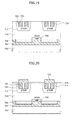
- FIGS. 10 to 20 are cross-sectional views illustrating a method of fabricating a vertical transistor having a P-type gallium nitride current barrier layer according to an exemplary embodiment of the present disclosure.
- a semiconductor layer 820 is formed on a first substrate 810.
- the first substrate 810 may be a growth substrate, for example, a sapphire substrate or a GaN substrate.
- the semiconductor layer 820 is formed of a GaN layer.
- the semiconductor layer 820 is patterned to form semiconductor patterns 822 that expose portions of the first substrate 810, as illustrated in FIG. 11 .
- Donor layers 714 are then formed on respective semiconductor patterns 822, as illustrated in FIG. 12 .
- the donor layers 714 may be formed of an N-type GaN layer.
- P-type GaN current barrier layers 712 are formed on respective donor layers 714.
- the P-type GaN current barrier layers 712 may be formed by doping a GaN layer with magnesium ions corresponding to a P-type dopant.
- the P-type GaN current barrier layers 712 are formed to cover sidewalls and top surfaces of the donor layers 714.
- a drift layer 710 is then formed on the P-type GaN current barrier layers 712.
- the drift layer 710 may be formed of an N-type GaN layer having an impurity concentration which is lower than that of the donor layers 714.
- current blocking patterns 706 are formed on the drift layer 710.
- the current blocking patterns 706 may be formed from a silicon oxide layer.
- the current blocking patterns 706 are formed to expose a portion of the drift layer 710.
- a low-resistance pattern 708 is formed on the exposed portion of the drift layer 710.
- the low-resistance pattern 708 may be formed of an N-type GaN layer having an impurity concentration which is higher than that of the drift layer 710.
- a dry etch process may be applied to the exposed portion of the drift layer 710. In such a case, the dry etch process may be performed using the current blocking patterns 706 as etch masks. As a result, an etch damage layer may be formed in the exposed portion of the drift layer 710 to act as the low-resistance pattern 708.
- a drain electrode 704 is formed on the current blocking patterns 706 and the low-resistance pattern 708, and a second substrate 702 is formed on or attached to the drain electrode 704.
- the second substrate 702 corresponds to a support substrate.
- a material of the second substrate 702 is not limited to any specific material.
- the first substrate 810 and the semiconductor patterns 822 is removed from the drift layer 710.
- a laser beam is radiated onto the first substrate 810, as denoted by arrows. The laser beam is irradiated with a sufficient energy to penetrate the first substrate 810 and the semiconductor patterns 822.
- a damaged layer 830 is formed at an interface between the first substrate 810 and the drift layer 710.
- the first substrate 810 and the semiconductor patterns 822 are lifted off and detached from the donor layers 714, the P-type GaN current barrier layers 712, and the drift layer 710, at the damaged layer 830.
- a dry etch process is then applied to the damaged layer 830 to remove the damaged layer 830, as denoted by arrows.
- the dry etch process for removing the damaged layer 830 may be performed using a reactive ion etching (RIE) technique.
- RIE reactive ion etching
- the donor layers 714 are patterned to form holes 722 exposing portions of the P-type GaN current barrier layers 712.
- the holes 722 may be formed using a photolithography process and an etch process. Specifically, a resist pattern (not shown) is formed on the drift layer 710 to have openings that expose portions of the donor layers 714. Subsequently, the exposed portions of the donor layers 714 may be etched using the resist pattern as an etch mask to form the holes 722, and the resist pattern may be removed.
- Each of the holes 722 is formed to have a circular shape in a plan view as illustrated in FIG. 7 or a rectangular shape in a plan view as illustrated in FIG. 9 .
- the holes 722 are formed such that distances between the holes 722 are less than or equal to 5 micrometers.
- a pulsed laser beam is irradiated onto the P-type GaN current barrier layers 712 through the holes 722.
- the pulsed laser beam activates the magnesium ions (acting as P-type dopants) in the P-type GaN current barrier layers 712 to remove hydrogen elements combined with the magnesium ions.
- the pulsed laser process may increase a temperature of metal materials, such as the magnesium, less, as compared with a general annealing processes, and may periodically irradiate the P-type GaN current barrier layers 712 without continuity.
- the pulsed laser process may minimize crystalline defects generated in the P-type GaN current barrier layers 712. That is, the pulsed laser process may improve characteristics of the P-type GaN current barrier layers 712 by activating the magnesium ions in the P-type GaN current barrier layers 712 without thermal damage and removing the hydrogen elements combined with the magnesium ions.
- the holes 722 are filled with a metal layer to form metal contact plugs 724 in respective ones of the holes 722.
- the metal contact plugs 724 are formed of a metal material having a good ohmic contact with respect to the P-type GaN current barrier layers 712.
- source electrodes 716 are formed on the metal contact plugs 724 and the donor layers 714.
- a gate insulation layer 718 is formed on top surfaces of the drift layer 710 and the P-type GaN current barrier layers 712.
- a gate electrode 720 is then formed on the gate insulation layer 718, as illustrated in FIG. 8 .
- a pulsed laser beam is irradiated onto P-type GaN current barrier layers exposed by holes to activate magnesium ions acting as P-type dopants in the P-type GaN current barrier layers, and to remove hydrogen combined with the magnesium ions.
- the pulsed laser process may increase a temperature of metal elements, such as the magnesium ions, less, as compared with general annealing processes, and may periodically apply a laser beam without continuity.
- the pulsed laser process may minimize crystalline defects generated in the P-type GaN current barrier layers. That is, the pulsed laser process may improve characteristics of the P-type GaN current barrier layers by activating the magnesium ions in the P-type GaN current barrier layers without thermal damage and removing the hydrogen combined with the magnesium ions.
Landscapes
- Junction Field-Effect Transistors (AREA)
- Electrodes Of Semiconductors (AREA)
- Thin Film Transistor (AREA)
Applications Claiming Priority (1)
| Application Number | Priority Date | Filing Date | Title |
|---|---|---|---|
| KR1020130081622A KR20150007546A (ko) | 2013-07-11 | 2013-07-11 | p형 갈륨나이트라이드 전류장벽층을 갖는 수직형 트랜지스터 및 그 제조방법 |
Publications (2)
| Publication Number | Publication Date |
|---|---|
| EP2824711A2 true EP2824711A2 (fr) | 2015-01-14 |
| EP2824711A3 EP2824711A3 (fr) | 2015-07-15 |
Family
ID=51176196
Family Applications (1)
| Application Number | Title | Priority Date | Filing Date |
|---|---|---|---|
| EP14176590.9A Withdrawn EP2824711A3 (fr) | 2013-07-11 | 2014-07-10 | Transistors verticaux disposant de couches de barrières de courant au nitrure de gallium de type P et leurs procédés de fabrication |
Country Status (5)
| Country | Link |
|---|---|
| US (1) | US20150014699A1 (fr) |
| EP (1) | EP2824711A3 (fr) |
| JP (1) | JP5805276B2 (fr) |
| KR (1) | KR20150007546A (fr) |
| CN (1) | CN104282746A (fr) |
Cited By (1)
| Publication number | Priority date | Publication date | Assignee | Title |
|---|---|---|---|---|
| CN109952656A (zh) * | 2016-11-11 | 2019-06-28 | 住友电气工业株式会社 | 碳化硅半导体器件 |
Families Citing this family (15)
| Publication number | Priority date | Publication date | Assignee | Title |
|---|---|---|---|---|
| CN105470294A (zh) * | 2015-12-08 | 2016-04-06 | 北京华进创威电子有限公司 | 一种垂直型氮化镓功率开关器件及其制备方法 |
| US10147813B2 (en) * | 2016-03-04 | 2018-12-04 | United Silicon Carbide, Inc. | Tunneling field effect transistor |
| WO2018076261A1 (fr) * | 2016-10-28 | 2018-05-03 | 华为技术有限公司 | Transistor à effet de champ et son procédé de fabrication |
| JP6906427B2 (ja) * | 2017-11-09 | 2021-07-21 | 株式会社豊田中央研究所 | 窒化物半導体装置とその製造方法 |
| JP7031238B2 (ja) * | 2017-11-09 | 2022-03-08 | 株式会社豊田中央研究所 | 窒化物半導体装置とその製造方法 |
| JP7157138B2 (ja) * | 2018-03-22 | 2022-10-19 | パナソニックホールディングス株式会社 | 窒化物半導体装置 |
| CN111129139B (zh) * | 2018-11-01 | 2021-03-30 | 西安电子科技大学 | 一种基于悬浮场板的自对准栅氮化镓增强型垂直功率器件 |
| JP2021114496A (ja) * | 2020-01-16 | 2021-08-05 | 信一郎 高谷 | 縦型窒化物半導体トランジスタ装置 |
| CN111584620A (zh) * | 2020-05-28 | 2020-08-25 | 西安电子科技大学芜湖研究院 | 一种降低p型mosfet源漏电极接触电阻的制备方法 |
| CN114078965B (zh) | 2020-08-11 | 2023-08-08 | 联华电子股份有限公司 | 高电子迁移率晶体管及其制作方法 |
| US11978790B2 (en) | 2020-12-01 | 2024-05-07 | Texas Instruments Incorporated | Normally-on gallium nitride based transistor with p-type gate |
| CN113030802B (zh) * | 2021-02-23 | 2023-05-16 | 南京邮电大学 | 一种基于类cavet晶体管结构的高灵敏度磁场传感器 |
| CN113539822B (zh) * | 2021-09-16 | 2022-01-28 | 浙江大学杭州国际科创中心 | 一种垂直电流孔径晶体管制备方法 |
| CN114503282B (zh) * | 2021-12-31 | 2024-01-02 | 英诺赛科(苏州)科技有限公司 | 氮化物基半导体装置及其制造方法 |
| JP2024126913A (ja) * | 2023-03-08 | 2024-09-20 | 株式会社デンソー | 窒化物半導体装置とその製造方法 |
Citations (1)
| Publication number | Priority date | Publication date | Assignee | Title |
|---|---|---|---|---|
| US20120319127A1 (en) | 2011-06-20 | 2012-12-20 | The Regents Of The University Of California | Current aperture vertical electron transistors with ammonia molecular beam epitaxy grown p-type gallium nitride as a current blocking layer |
Family Cites Families (4)
| Publication number | Priority date | Publication date | Assignee | Title |
|---|---|---|---|---|
| JP2004055869A (ja) * | 2002-07-22 | 2004-02-19 | Nec Corp | 半導体装置 |
| JP2009117820A (ja) * | 2007-10-16 | 2009-05-28 | Rohm Co Ltd | 窒化物半導体素子および窒化物半導体素子の製造方法 |
| US8981434B2 (en) * | 2009-08-31 | 2015-03-17 | Renesas Electronics Corporation | Semiconductor device and field effect transistor |
| JP4985760B2 (ja) * | 2009-12-28 | 2012-07-25 | 住友電気工業株式会社 | 半導体装置およびその製造方法 |
-
2013
- 2013-07-11 KR KR1020130081622A patent/KR20150007546A/ko not_active Ceased
-
2014
- 2014-07-09 CN CN201410325340.1A patent/CN104282746A/zh active Pending
- 2014-07-09 US US14/327,204 patent/US20150014699A1/en not_active Abandoned
- 2014-07-10 JP JP2014142115A patent/JP5805276B2/ja active Active
- 2014-07-10 EP EP14176590.9A patent/EP2824711A3/fr not_active Withdrawn
Patent Citations (1)
| Publication number | Priority date | Publication date | Assignee | Title |
|---|---|---|---|---|
| US20120319127A1 (en) | 2011-06-20 | 2012-12-20 | The Regents Of The University Of California | Current aperture vertical electron transistors with ammonia molecular beam epitaxy grown p-type gallium nitride as a current blocking layer |
Cited By (1)
| Publication number | Priority date | Publication date | Assignee | Title |
|---|---|---|---|---|
| CN109952656A (zh) * | 2016-11-11 | 2019-06-28 | 住友电气工业株式会社 | 碳化硅半导体器件 |
Also Published As
| Publication number | Publication date |
|---|---|
| JP5805276B2 (ja) | 2015-11-04 |
| US20150014699A1 (en) | 2015-01-15 |
| JP2015019070A (ja) | 2015-01-29 |
| EP2824711A3 (fr) | 2015-07-15 |
| KR20150007546A (ko) | 2015-01-21 |
| CN104282746A (zh) | 2015-01-14 |
Similar Documents
| Publication | Publication Date | Title |
|---|---|---|
| EP2824711A2 (fr) | Transistors verticaux disposant de couches de barrières de courant au nitrure de gallium de type P et leurs procédés de fabrication | |
| US7982224B2 (en) | Semiconductor device with silicon carbide epitaxial layer including dopant profiles for reducing current overconcentration | |
| EP2793255B1 (fr) | Procédé de fabrication d'un dispositif semi-conducteur comprenant une diode schottky et un transistor à haute mobilité d'électrons | |
| US9184305B2 (en) | Method and system for a GAN vertical JFET utilizing a regrown gate | |
| JP5685736B2 (ja) | 半導体装置及びその製造方法 | |
| US9224828B2 (en) | Method and system for floating guard rings in gallium nitride materials | |
| US8969912B2 (en) | Method and system for a GaN vertical JFET utilizing a regrown channel | |
| US8829574B2 (en) | Method and system for a GaN vertical JFET with self-aligned source and gate | |
| US9502544B2 (en) | Method and system for planar regrowth in GaN electronic devices | |
| EP3284107B1 (fr) | Transistor au nitrure du groupe iii comportant une grille de tranchée | |
| US9059199B2 (en) | Method and system for a gallium nitride vertical transistor | |
| EP2843708A1 (fr) | Transistors à base de nitrure et procédés de fabrication de celui-ci | |
| US9660046B2 (en) | Method of manufacturing semiconductor device | |
| WO2017145548A1 (fr) | Dispositif à semi-conducteur composé et son procédé de fabrication | |
| US8835935B2 (en) | Trench MOS transistor having a trench doped region formed deeper than the trench gate | |
| US20140103439A1 (en) | Transistor Device and Method for Producing a Transistor Device | |
| US20140191241A1 (en) | Gallium nitride vertical jfet with hexagonal cell structure | |
| CN112447834B (zh) | 半导体器件及其制造方法 | |
| US20130164893A1 (en) | Fabrication of floating guard rings using selective regrowth | |
| KR102100863B1 (ko) | SiC MOSFET 전력 반도체 소자 | |
| US20140145201A1 (en) | Method and system for gallium nitride vertical jfet with separated gate and source | |
| KR102067596B1 (ko) | 질화물 반도체 소자 및 그 제조 방법 | |
| US10418477B2 (en) | Silicon carbide semiconductor device and method of manufacturing silicon carbide semiconductor device | |
| CN116895531A (zh) | 碳化硅场效应晶体管的制备方法及碳化硅场效应晶体管 | |
| KR20150011190A (ko) | 질화물계 전계효과 트랜지스터 및 그 제조방법 |
Legal Events
| Date | Code | Title | Description |
|---|---|---|---|
| 17P | Request for examination filed |
Effective date: 20140710 |
|
| AK | Designated contracting states |
Kind code of ref document: A2 Designated state(s): AL AT BE BG CH CY CZ DE DK EE ES FI FR GB GR HR HU IE IS IT LI LT LU LV MC MK MT NL NO PL PT RO RS SE SI SK SM TR |
|
| AX | Request for extension of the european patent |
Extension state: BA ME |
|
| PUAI | Public reference made under article 153(3) epc to a published international application that has entered the european phase |
Free format text: ORIGINAL CODE: 0009012 |
|
| RIC1 | Information provided on ipc code assigned before grant |
Ipc: H01L 29/417 20060101ALI20150219BHEP Ipc: H01L 29/06 20060101ALI20150219BHEP Ipc: H01L 21/683 20060101ALI20150219BHEP Ipc: H01L 21/268 20060101ALI20150219BHEP Ipc: H01L 29/20 20060101ALN20150219BHEP Ipc: H01L 29/08 20060101ALN20150219BHEP Ipc: H01L 29/78 20060101AFI20150219BHEP Ipc: H01L 29/778 20060101ALI20150219BHEP Ipc: H01L 21/336 20060101ALI20150219BHEP |
|
| PUAL | Search report despatched |
Free format text: ORIGINAL CODE: 0009013 |
|
| AK | Designated contracting states |
Kind code of ref document: A3 Designated state(s): AL AT BE BG CH CY CZ DE DK EE ES FI FR GB GR HR HU IE IS IT LI LT LU LV MC MK MT NL NO PL PT RO RS SE SI SK SM TR |
|
| AX | Request for extension of the european patent |
Extension state: BA ME |
|
| RIC1 | Information provided on ipc code assigned before grant |
Ipc: H01L 21/336 20060101ALI20150611BHEP Ipc: H01L 29/78 20060101AFI20150611BHEP Ipc: H01L 29/778 20060101ALI20150611BHEP Ipc: H01L 29/417 20060101ALI20150611BHEP Ipc: H01L 29/08 20060101ALN20150611BHEP Ipc: H01L 21/683 20060101ALI20150611BHEP Ipc: H01L 29/20 20060101ALN20150611BHEP Ipc: H01L 21/268 20060101ALI20150611BHEP Ipc: H01L 29/06 20060101ALI20150611BHEP |
|
| RBV | Designated contracting states (corrected) |
Designated state(s): AL AT BE BG CH CY CZ DE DK EE ES FI FR GB GR HR HU IE IS IT LI LT LU LV MC MK MT NL NO PL PT RO RS SE SI SK SM TR |
|
| STAA | Information on the status of an ep patent application or granted ep patent |
Free format text: STATUS: THE APPLICATION IS DEEMED TO BE WITHDRAWN |
|
| 18D | Application deemed to be withdrawn |
Effective date: 20160116 |