EP2827323A2 - Configuration d'une programmation par tension pour écrans amoled alimentés par courant - Google Patents
Configuration d'une programmation par tension pour écrans amoled alimentés par courant Download PDFInfo
- Publication number
- EP2827323A2 EP2827323A2 EP14181848.4A EP14181848A EP2827323A2 EP 2827323 A2 EP2827323 A2 EP 2827323A2 EP 14181848 A EP14181848 A EP 14181848A EP 2827323 A2 EP2827323 A2 EP 2827323A2
- Authority
- EP
- European Patent Office
- Prior art keywords
- voltage
- pixel circuit
- current
- programming
- data
- Prior art date
- Legal status (The legal status is an assumption and is not a legal conclusion. Google has not performed a legal analysis and makes no representation as to the accuracy of the status listed.)
- Ceased
Links
Images










Classifications
-
- G—PHYSICS
- G09—EDUCATION; CRYPTOGRAPHY; DISPLAY; ADVERTISING; SEALS
- G09G—ARRANGEMENTS OR CIRCUITS FOR CONTROL OF INDICATING DEVICES USING STATIC MEANS TO PRESENT VARIABLE INFORMATION
- G09G3/00—Control arrangements or circuits, of interest only in connection with visual indicators other than cathode-ray tubes
- G09G3/20—Control arrangements or circuits, of interest only in connection with visual indicators other than cathode-ray tubes for presentation of an assembly of a number of characters, e.g. a page, by composing the assembly by combination of individual elements arranged in a matrix no fixed position being assigned to or needed to be assigned to the individual characters or partial characters
- G09G3/22—Control arrangements or circuits, of interest only in connection with visual indicators other than cathode-ray tubes for presentation of an assembly of a number of characters, e.g. a page, by composing the assembly by combination of individual elements arranged in a matrix no fixed position being assigned to or needed to be assigned to the individual characters or partial characters using controlled light sources
- G09G3/30—Control arrangements or circuits, of interest only in connection with visual indicators other than cathode-ray tubes for presentation of an assembly of a number of characters, e.g. a page, by composing the assembly by combination of individual elements arranged in a matrix no fixed position being assigned to or needed to be assigned to the individual characters or partial characters using controlled light sources using electroluminescent panels
- G09G3/32—Control arrangements or circuits, of interest only in connection with visual indicators other than cathode-ray tubes for presentation of an assembly of a number of characters, e.g. a page, by composing the assembly by combination of individual elements arranged in a matrix no fixed position being assigned to or needed to be assigned to the individual characters or partial characters using controlled light sources using electroluminescent panels semiconductive, e.g. using light-emitting diodes [LED]
- G09G3/3208—Control arrangements or circuits, of interest only in connection with visual indicators other than cathode-ray tubes for presentation of an assembly of a number of characters, e.g. a page, by composing the assembly by combination of individual elements arranged in a matrix no fixed position being assigned to or needed to be assigned to the individual characters or partial characters using controlled light sources using electroluminescent panels semiconductive, e.g. using light-emitting diodes [LED] organic, e.g. using organic light-emitting diodes [OLED]
- G09G3/3225—Control arrangements or circuits, of interest only in connection with visual indicators other than cathode-ray tubes for presentation of an assembly of a number of characters, e.g. a page, by composing the assembly by combination of individual elements arranged in a matrix no fixed position being assigned to or needed to be assigned to the individual characters or partial characters using controlled light sources using electroluminescent panels semiconductive, e.g. using light-emitting diodes [LED] organic, e.g. using organic light-emitting diodes [OLED] using an active matrix
- G09G3/3233—Control arrangements or circuits, of interest only in connection with visual indicators other than cathode-ray tubes for presentation of an assembly of a number of characters, e.g. a page, by composing the assembly by combination of individual elements arranged in a matrix no fixed position being assigned to or needed to be assigned to the individual characters or partial characters using controlled light sources using electroluminescent panels semiconductive, e.g. using light-emitting diodes [LED] organic, e.g. using organic light-emitting diodes [OLED] using an active matrix with pixel circuitry controlling the current through the light-emitting element
-
- G—PHYSICS
- G09—EDUCATION; CRYPTOGRAPHY; DISPLAY; ADVERTISING; SEALS
- G09G—ARRANGEMENTS OR CIRCUITS FOR CONTROL OF INDICATING DEVICES USING STATIC MEANS TO PRESENT VARIABLE INFORMATION
- G09G3/00—Control arrangements or circuits, of interest only in connection with visual indicators other than cathode-ray tubes
- G09G3/20—Control arrangements or circuits, of interest only in connection with visual indicators other than cathode-ray tubes for presentation of an assembly of a number of characters, e.g. a page, by composing the assembly by combination of individual elements arranged in a matrix no fixed position being assigned to or needed to be assigned to the individual characters or partial characters
- G09G3/22—Control arrangements or circuits, of interest only in connection with visual indicators other than cathode-ray tubes for presentation of an assembly of a number of characters, e.g. a page, by composing the assembly by combination of individual elements arranged in a matrix no fixed position being assigned to or needed to be assigned to the individual characters or partial characters using controlled light sources
- G09G3/30—Control arrangements or circuits, of interest only in connection with visual indicators other than cathode-ray tubes for presentation of an assembly of a number of characters, e.g. a page, by composing the assembly by combination of individual elements arranged in a matrix no fixed position being assigned to or needed to be assigned to the individual characters or partial characters using controlled light sources using electroluminescent panels
- G09G3/32—Control arrangements or circuits, of interest only in connection with visual indicators other than cathode-ray tubes for presentation of an assembly of a number of characters, e.g. a page, by composing the assembly by combination of individual elements arranged in a matrix no fixed position being assigned to or needed to be assigned to the individual characters or partial characters using controlled light sources using electroluminescent panels semiconductive, e.g. using light-emitting diodes [LED]
- G09G3/3208—Control arrangements or circuits, of interest only in connection with visual indicators other than cathode-ray tubes for presentation of an assembly of a number of characters, e.g. a page, by composing the assembly by combination of individual elements arranged in a matrix no fixed position being assigned to or needed to be assigned to the individual characters or partial characters using controlled light sources using electroluminescent panels semiconductive, e.g. using light-emitting diodes [LED] organic, e.g. using organic light-emitting diodes [OLED]
- G09G3/3225—Control arrangements or circuits, of interest only in connection with visual indicators other than cathode-ray tubes for presentation of an assembly of a number of characters, e.g. a page, by composing the assembly by combination of individual elements arranged in a matrix no fixed position being assigned to or needed to be assigned to the individual characters or partial characters using controlled light sources using electroluminescent panels semiconductive, e.g. using light-emitting diodes [LED] organic, e.g. using organic light-emitting diodes [OLED] using an active matrix
- G09G3/3233—Control arrangements or circuits, of interest only in connection with visual indicators other than cathode-ray tubes for presentation of an assembly of a number of characters, e.g. a page, by composing the assembly by combination of individual elements arranged in a matrix no fixed position being assigned to or needed to be assigned to the individual characters or partial characters using controlled light sources using electroluminescent panels semiconductive, e.g. using light-emitting diodes [LED] organic, e.g. using organic light-emitting diodes [OLED] using an active matrix with pixel circuitry controlling the current through the light-emitting element
- G09G3/3241—Control arrangements or circuits, of interest only in connection with visual indicators other than cathode-ray tubes for presentation of an assembly of a number of characters, e.g. a page, by composing the assembly by combination of individual elements arranged in a matrix no fixed position being assigned to or needed to be assigned to the individual characters or partial characters using controlled light sources using electroluminescent panels semiconductive, e.g. using light-emitting diodes [LED] organic, e.g. using organic light-emitting diodes [OLED] using an active matrix with pixel circuitry controlling the current through the light-emitting element the current through the light-emitting element being set using a data current provided by the data driver, e.g. by using a two-transistor current mirror
-
- G—PHYSICS
- G09—EDUCATION; CRYPTOGRAPHY; DISPLAY; ADVERTISING; SEALS
- G09G—ARRANGEMENTS OR CIRCUITS FOR CONTROL OF INDICATING DEVICES USING STATIC MEANS TO PRESENT VARIABLE INFORMATION
- G09G3/00—Control arrangements or circuits, of interest only in connection with visual indicators other than cathode-ray tubes
- G09G3/20—Control arrangements or circuits, of interest only in connection with visual indicators other than cathode-ray tubes for presentation of an assembly of a number of characters, e.g. a page, by composing the assembly by combination of individual elements arranged in a matrix no fixed position being assigned to or needed to be assigned to the individual characters or partial characters
- G09G3/22—Control arrangements or circuits, of interest only in connection with visual indicators other than cathode-ray tubes for presentation of an assembly of a number of characters, e.g. a page, by composing the assembly by combination of individual elements arranged in a matrix no fixed position being assigned to or needed to be assigned to the individual characters or partial characters using controlled light sources
- G09G3/30—Control arrangements or circuits, of interest only in connection with visual indicators other than cathode-ray tubes for presentation of an assembly of a number of characters, e.g. a page, by composing the assembly by combination of individual elements arranged in a matrix no fixed position being assigned to or needed to be assigned to the individual characters or partial characters using controlled light sources using electroluminescent panels
- G09G3/32—Control arrangements or circuits, of interest only in connection with visual indicators other than cathode-ray tubes for presentation of an assembly of a number of characters, e.g. a page, by composing the assembly by combination of individual elements arranged in a matrix no fixed position being assigned to or needed to be assigned to the individual characters or partial characters using controlled light sources using electroluminescent panels semiconductive, e.g. using light-emitting diodes [LED]
- G09G3/3208—Control arrangements or circuits, of interest only in connection with visual indicators other than cathode-ray tubes for presentation of an assembly of a number of characters, e.g. a page, by composing the assembly by combination of individual elements arranged in a matrix no fixed position being assigned to or needed to be assigned to the individual characters or partial characters using controlled light sources using electroluminescent panels semiconductive, e.g. using light-emitting diodes [LED] organic, e.g. using organic light-emitting diodes [OLED]
- G09G3/3275—Details of drivers for data electrodes
- G09G3/3283—Details of drivers for data electrodes in which the data driver supplies a variable data current for setting the current through, or the voltage across, the light-emitting elements
-
- G—PHYSICS
- G09—EDUCATION; CRYPTOGRAPHY; DISPLAY; ADVERTISING; SEALS
- G09G—ARRANGEMENTS OR CIRCUITS FOR CONTROL OF INDICATING DEVICES USING STATIC MEANS TO PRESENT VARIABLE INFORMATION
- G09G3/00—Control arrangements or circuits, of interest only in connection with visual indicators other than cathode-ray tubes
- G09G3/20—Control arrangements or circuits, of interest only in connection with visual indicators other than cathode-ray tubes for presentation of an assembly of a number of characters, e.g. a page, by composing the assembly by combination of individual elements arranged in a matrix no fixed position being assigned to or needed to be assigned to the individual characters or partial characters
- G09G3/22—Control arrangements or circuits, of interest only in connection with visual indicators other than cathode-ray tubes for presentation of an assembly of a number of characters, e.g. a page, by composing the assembly by combination of individual elements arranged in a matrix no fixed position being assigned to or needed to be assigned to the individual characters or partial characters using controlled light sources
- G09G3/30—Control arrangements or circuits, of interest only in connection with visual indicators other than cathode-ray tubes for presentation of an assembly of a number of characters, e.g. a page, by composing the assembly by combination of individual elements arranged in a matrix no fixed position being assigned to or needed to be assigned to the individual characters or partial characters using controlled light sources using electroluminescent panels
- G09G3/32—Control arrangements or circuits, of interest only in connection with visual indicators other than cathode-ray tubes for presentation of an assembly of a number of characters, e.g. a page, by composing the assembly by combination of individual elements arranged in a matrix no fixed position being assigned to or needed to be assigned to the individual characters or partial characters using controlled light sources using electroluminescent panels semiconductive, e.g. using light-emitting diodes [LED]
- G09G3/3208—Control arrangements or circuits, of interest only in connection with visual indicators other than cathode-ray tubes for presentation of an assembly of a number of characters, e.g. a page, by composing the assembly by combination of individual elements arranged in a matrix no fixed position being assigned to or needed to be assigned to the individual characters or partial characters using controlled light sources using electroluminescent panels semiconductive, e.g. using light-emitting diodes [LED] organic, e.g. using organic light-emitting diodes [OLED]
- G09G3/3275—Details of drivers for data electrodes
- G09G3/3291—Details of drivers for data electrodes in which the data driver supplies a variable data voltage for setting the current through, or the voltage across, the light-emitting elements
-
- G—PHYSICS
- G09—EDUCATION; CRYPTOGRAPHY; DISPLAY; ADVERTISING; SEALS
- G09G—ARRANGEMENTS OR CIRCUITS FOR CONTROL OF INDICATING DEVICES USING STATIC MEANS TO PRESENT VARIABLE INFORMATION
- G09G2300/00—Aspects of the constitution of display devices
- G09G2300/08—Active matrix structure, i.e. with use of active elements, inclusive of non-linear two terminal elements, in the pixels together with light emitting or modulating elements
- G09G2300/0809—Several active elements per pixel in active matrix panels
- G09G2300/0842—Several active elements per pixel in active matrix panels forming a memory circuit, e.g. a dynamic memory with one capacitor
-
- G—PHYSICS
- G09—EDUCATION; CRYPTOGRAPHY; DISPLAY; ADVERTISING; SEALS
- G09G—ARRANGEMENTS OR CIRCUITS FOR CONTROL OF INDICATING DEVICES USING STATIC MEANS TO PRESENT VARIABLE INFORMATION
- G09G2300/00—Aspects of the constitution of display devices
- G09G2300/08—Active matrix structure, i.e. with use of active elements, inclusive of non-linear two terminal elements, in the pixels together with light emitting or modulating elements
- G09G2300/0809—Several active elements per pixel in active matrix panels
- G09G2300/0842—Several active elements per pixel in active matrix panels forming a memory circuit, e.g. a dynamic memory with one capacitor
- G09G2300/0861—Several active elements per pixel in active matrix panels forming a memory circuit, e.g. a dynamic memory with one capacitor with additional control of the display period without amending the charge stored in a pixel memory, e.g. by means of additional select electrodes
-
- G—PHYSICS
- G09—EDUCATION; CRYPTOGRAPHY; DISPLAY; ADVERTISING; SEALS
- G09G—ARRANGEMENTS OR CIRCUITS FOR CONTROL OF INDICATING DEVICES USING STATIC MEANS TO PRESENT VARIABLE INFORMATION
- G09G2310/00—Command of the display device
- G09G2310/02—Addressing, scanning or driving the display screen or processing steps related thereto
- G09G2310/0243—Details of the generation of driving signals
- G09G2310/0251—Precharge or discharge of pixel before applying new pixel voltage
-
- G—PHYSICS
- G09—EDUCATION; CRYPTOGRAPHY; DISPLAY; ADVERTISING; SEALS
- G09G—ARRANGEMENTS OR CIRCUITS FOR CONTROL OF INDICATING DEVICES USING STATIC MEANS TO PRESENT VARIABLE INFORMATION
- G09G2310/00—Command of the display device
- G09G2310/02—Addressing, scanning or driving the display screen or processing steps related thereto
- G09G2310/0264—Details of driving circuits
- G09G2310/027—Details of drivers for data electrodes, the drivers handling digital grey scale data, e.g. use of D/A converters
-
- G—PHYSICS
- G09—EDUCATION; CRYPTOGRAPHY; DISPLAY; ADVERTISING; SEALS
- G09G—ARRANGEMENTS OR CIRCUITS FOR CONTROL OF INDICATING DEVICES USING STATIC MEANS TO PRESENT VARIABLE INFORMATION
- G09G2320/00—Control of display operating conditions
- G09G2320/02—Improving the quality of display appearance
- G09G2320/0285—Improving the quality of display appearance using tables for spatial correction of display data
-
- G—PHYSICS
- G09—EDUCATION; CRYPTOGRAPHY; DISPLAY; ADVERTISING; SEALS
- G09G—ARRANGEMENTS OR CIRCUITS FOR CONTROL OF INDICATING DEVICES USING STATIC MEANS TO PRESENT VARIABLE INFORMATION
- G09G2320/00—Control of display operating conditions
- G09G2320/02—Improving the quality of display appearance
- G09G2320/029—Improving the quality of display appearance by monitoring one or more pixels in the display panel, e.g. by monitoring a fixed reference pixel
- G09G2320/0295—Improving the quality of display appearance by monitoring one or more pixels in the display panel, e.g. by monitoring a fixed reference pixel by monitoring each display pixel
-
- G—PHYSICS
- G09—EDUCATION; CRYPTOGRAPHY; DISPLAY; ADVERTISING; SEALS
- G09G—ARRANGEMENTS OR CIRCUITS FOR CONTROL OF INDICATING DEVICES USING STATIC MEANS TO PRESENT VARIABLE INFORMATION
- G09G2320/00—Control of display operating conditions
- G09G2320/04—Maintaining the quality of display appearance
- G09G2320/043—Preventing or counteracting the effects of ageing
-
- G—PHYSICS
- G09—EDUCATION; CRYPTOGRAPHY; DISPLAY; ADVERTISING; SEALS
- G09G—ARRANGEMENTS OR CIRCUITS FOR CONTROL OF INDICATING DEVICES USING STATIC MEANS TO PRESENT VARIABLE INFORMATION
- G09G2320/00—Control of display operating conditions
- G09G2320/06—Adjustment of display parameters
- G09G2320/0693—Calibration of display systems
Definitions
- the present invention relates to a display technique, and more specifically to technology for driving pixel circuits.
- AMOLED Active matrix organic light emitting diode
- the AMOLED displays are classified as either a voltage-programmed display or a current-programmed display.
- the voltage-programmed display is driven by a voltage-programmed scheme where data is applied to the display as a voltage.
- the current-programmed display is driven by a current-programmed scheme where data is applied to the display as a current.
- the advantage of the current-programming scheme is that it can facilitate pixel designs where the brightness of the pixel remains more constant over time than with voltage programming.
- the current-programming requires longer time of charging capacitors associated with the column.
- the present invention relates to a system and method of driving a pixel circuit in an AMOLED display.
- the system and method of the present invention uses Voltage-Programniing Scheme For Current-Driven AMOLED Displays.
- a system for driving a display which includes a plurality of pixel circuits, each having a plurality of thin film transistors (TFTs) and an organic light emitting diode (OLED), which includes: a voltage driver for generating a voltage to program the pixel circuit; a programmable current source for generating a current to program the pixel circuit; and a switching network for selectively connecting the data driver or the current source to one or more pixel circuits.
- TFTs thin film transistors
- OLED organic light emitting diode
- a system for driving a pixel circuit having a plurality of thin film transistors (TFTs) and an organic light emitting diode (OLED), which includes: a pre-charge controller for pre-charging and discharging a data node of the pixel circuit to acquire threshold voltage information of the TFT from the data node; and a hybrid driving circuit for programming the pixel circuit based on the acquired threshold voltage information and video data information displayed on the pixel circuit.
- TFTs thin film transistors
- OLED organic light emitting diode
- a system for driving a pixel circuit having a plurality of thin film transistors (TFTs) and an organic light emitting diode (OLED), which includes: a sampler for sampling, from a data node of the pixel circuit, a voltage required to program the pixel circuit; and a programming circuit for programming the pixel circuit based on the sampled voltage and video data information displayed on the pixel circuit.
- TFTs thin film transistors
- OLED organic light emitting diode
- a method of driving a pixel circuit having a plurality of thin film transistors (TFTs) and an organic light emitting diode (OLED), which includes the steps of: selecting a pixel circuit and pre-charging a data node of the pixel circuit; allowing the pre-charged data node to be discharged; extracting a threshold voltage of the TFT through the discharging step; and programming the pixel circuit, including compensating a programming data based on the extracted threshold voltage.
- TFTs thin film transistors
- OLED organic light emitting diode
- Embodiments of the present invention are described using an AMOLED display. Drive scheme described below is applicable to a current programmed (driven) pixel circuit and a voltage programmed (driven) pixel circuit.
- hybrid technique described below can be applied any existing driving scheme, including a) any drive schemes that use sophisticated timing of the data, select, or power inputs to the pixels to achieve increased brightness uniformity, b) any drive schemes that use current or voltage feedback, c) any drive schemes that use optical feedback.
- the light emitting material of the pixel circuit can be any technology, specifically organic light emitting diode (OLED) technology, and in particular, but not limited to, fluorescent, phosphorescent, polymer, and dendrimer materials.
- OLED organic light emitting diode
- FIG. 1 there is illustrated a system 2 for driving an AMOLED display 5 in accordance with an embodiment of the present invention.
- the AMOLED display 5 includes a plurality of pixel circuits.
- four pixel circuits 10 are shown as an example.
- the system 2 includes a hybrid driving circuit 12, a voltage source driver 14, a hybrid programming controller 16, a gate driver 18A and a power-supply 18B.
- the pixel circuit 10 is selected by the gate driver 18A (Vsel), and is programmed by either voltage mode using a node Vdata or current mode using a node Idata.
- the hybrid driving circuit 12 selects the mode of programming, and connects it to the pixel circuit 10 through a hybrid signal.
- a pre-charge signal (Vp) is applied to the pixel circuit 10 to acquire threshold Vt information (or Vt shift information) from the pixel circuit 10.
- the hybrid driving circuit 12 controls the pre-charging, if pre-charging technique is used.
- the pre-charge signal (Vp) may be generated within the hybrid driving circuit 12, which depends on the operation condition.
- the power-supply 18B (Vdd) supplies the current required to energize the display 5 and to monitor the power consumption of the display 5.
- the hybrid controller 16 controls the individual components that make up the entire hybrid programming circuit.
- the hybrid controller 16 handles timing and controls the order in which the required functions occur.
- the hybrid controller 16 may generate data Idata and supplied to the hybrid driving circuit 12.
- the system 2 may have a reference current source, and the Idata may be supplied under the control of the hybrid controller 16.
- the hybrid driven 12 may be implemented either as a switching matrix, or as the hybrid driving circuit(s) of Figure 3 , 6 , 8 or 20 or combination thereof.
- Vdata refers to data, a data signal, a data line or a node for supplying the data or data signal Vdata, or a voltage on the data line or the node.
- Idata refers to data, a data signal, a data line or a node for supplying the data or data signal Idata, or a current on the data line or the node.
- Vp refers to a pre-charge signal, a pre-charge pulse, a pre-charge voltage for pre-charging/discharging, a line or a node for supplying the pre-charge signal, pre-charge pulse or pre-charge voltage Vp.
- Vsel refers to a pulse or a signal for selecting a pixel circuit or a line or a node for supplying the pulse or signal Vs.
- the terms "hybrid signal”, “hybrid signal node”, and “hybrid signal line” may be used interchangeably.
- the pixel circuit 10 includes a plurality of TFTs, and an organic light emitting diode (OLED).
- the TFT may be an n-type TFT or a p-type TFT.
- the TFT is, for example, but not limited to, an amorphous silicon (a-Si:H) based TFT, a polycrystalline silicon based TFT, a crystalline silicon based TFT, or an organic semiconductor based TFT.
- the OLED may be regular (P-I-N) stack or inverted (N-I-P) stack.
- the OLED can be located in the source or the drain of one or more driving TFTs.
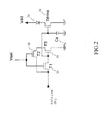
- FIG. 2 illustrates an example of the pixel circuit 10 of Figure 1 .
- the pixel circuit of Figure 2 includes four thin film transistors (TFTs) 20-26, a capacitor Cs 28 and an organic light emitter diode (OLED) 30.
- the TFT (Tdrive) 26 is a drive TFT that is connected to the OLED 30 and the capacitor Cs 28.
- the pixel circuit of Figure 2 is selected by the select line Vsel, and is programmed by a data line DL.
- the data line DL is controlled by the hybrid signal output from the hybrid driving circuit 12 of Figure 1 .
- the pixel circuit 10 of Figure 1 may include less than four TFTs or more than four TFTs.
- data line DL and “data node DL” may be used interchangeably.
- the data node DL is pre-charged and discharged to acquire the threshold Vt of a drive TFT (e.g., Tdrive 26 of Figure 2 ) or the threshold Vt shift.
- Vt shift, Vt shift information, Vt, and Vt information may be used interchangeably.
- the pixel circuit 10 is then consecutively programmed by the source driver 14 using voltage-programming. The acquired Vt shift information is utilized to compensate for degradation of the pixel circuit 10, thus maintaining uniform brightness of the display 5.
- the process of acquiring Vt starts by applying Vsel to T1 20 and T2 22 to the pixel circuit illustrated in Figure 2 .
- Such action causes the drain and gate of T3 24 to be at the same voltage.
- This allows the Vt of T3 24 to be extracted by first applying the pre-charge voltage Vp to the data line DL, which is than allowed to be discharged.
- the rate of discharge is a function of Vt.
- Vt can be obtained.
- FIG 3 illustrates an example of a hybrid driving circuit, which is applicable to the hybrid driving circuit 12 of Figure 1 .
- the hybrid driving circuit 12A of Figure 3 implements voltage programming technique.
- the hybrid driving circuit 12A of Figure 3 includes a charge programming capacitor Cc 32.
- the charge programming capacitor Cc 32 is provided between the data line Vdata and the data node DL.
- the pre-charge line Vp is also connected to the data node DL.
- the hybrid driving circuit 12A is provided to a pixel circuit 10A having four TFTs (such as the pixel circuit of Figure 2 ).
- the pixel circuit 10A may include more than four TFTs or less than four TFTs.
- the charge programming capacitor Cc 32 is provided to program the pixel circuit 10A with a voltage that is equal to the sum of threshold Vt of the TFT and Vdata, scaled by a constant K.
- the constant is determined by the voltage division network formed by the charge storage capacitor (e.g. Cs 28 of Figure 2 ) and the charge programming capacitor Cc 32.
- FIG. 4 illustrates an exemplary flow chart for showing the operation of the hybrid driving circuit 12A of Figure 3 .
- pre-charge mode is enabled.
- a pixel circuit is selected and pre-charging (Vp) is started.
- Vt acquisition mode is enabled, and at step S16, discharging (Vp) starts.
- the Vt information is acquired through Cc 32.
- writing mode is enabled.
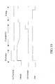
- Figure 5 illustrates an exemplary timing chart for showing the operation of the hybrid driving circuit 12A of Figure 3 .
- Vdata0 represents voltage at the data node (e.g. DL of Figure 2 ) of the pixel circuit
- Idata0 represents current at the data node (e.g. DL of Figure 2 ) of the pixel circuit.
- the programming procedure starts by selecting the pixel to be programmed with the pulse Vsel.
- the pre-charge pulse Vp is applied to the pixel circuit's data input (e.g. DL of Figure 2 ).
- Vt acquisition phase voltage on the data line (DL) is allowed to be discharged through the pixel circuit, which is in a current mirror connection with the Vsel line held high.
- the data line (DL) is discharged to a certain voltage, and the Vt of a drive TFT is extracted from that voltage.
- the voltage at Vdata is at ground.
- the calculated compensated voltage is applied to the data input line (DL) of the pixel circuit.
- the programming routine finishes with the lowering of the Vsel signal.
- the calculated compensated voltage is obtained through analog means of a charge programming capacitor Cc32.
- any other analog means for obtaining compensated voltage may be used.
- any (external) digital circuit e.g. 50 of Figure 7 ) may be used to obtain the calculated compensated voltage.
- the source driver (14 of Figure 1 ) supplies Vdata to the capacitor Cc 32.
- Vdata is increased from ground to the desired voltage level, the voltage at Idata is equal to (Vt+Vdata)*K.
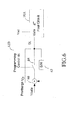
- FIG. 6 illustrates a further example of a hybrid driving circuit, which is applicable to the hybrid driving circuit 12 of Figure 1 .
- the hybrid driving circuit 12B of Figure 6 implements voltage programming technique.
- the hybrid driving circuit 12B includes a summer 40, a sample and hold (S/H) circuit 42 and a switching element 44.
- the S/H circuit 42 samples Idata and holds it for a certain period.
- the summer 40 receives Vdata and the output of the S/H circuit 42.
- the switching element 44 connects the output of the summer 40 to the data node DL in response to a programming control signal 46.
- the hybrid driving circuit 12B utilizes the summer 40, instead of the charge coupling capacitor Cc 32, to produce programming voltage that is equal to the sum of Vt and Vdata.
- the hybrid driving circuit 12B does not utilize a capacity, programming voltage is not affected by the parasitic capacitance, and it has less charge feed-through effect.
- the hybrid driving circuit 12B does not utilize a charge storage capacitor, programming voltage is not affected by the charge storage capacitance.
- the hybrid driving circuit 12B does not utilize a charge programming capacitor, it achieves faster Vt acquisition time. Removal of the charge programming capacitor eliminates the charge dependency of the programming scheme. Thus the programming voltage is not affected by the charge being shared between the charge storage capacitor and the parasitic capacitance of the system. This results in a higher effective programming voltage.
- Figure 7 illustrates an exemplary flow chart for showing the operation of the hybrid driving circuit 12B of Figure 6 .
- the Vt is sampled at step S20, and new data is produced at step S22.
- the new data is supplied to the pixel circuit in response to the programming control signal (46) at S24. It is noted that the operation of the system having the hybrid driving circuit 12B is not limited to Figure 7 .
- the new data may be produced after step S18.
- the control signal 46 may be enabled before step S18.
- Vdata is at ground, and the voltage at the data node DL is equal to Vt of the TFT by the pre-charging/discharging operation (Vp).
- the voltage on the data node DL is sampled and holed by the S/H circuit 42.
- the Vt is provided to the summer 40 through the S/H circuit 42.
- the summer 40 outputs the sum of Vt and Vdata.
- the switch 44 turns on in response to the programming control signal 46.
- the voltage at the data node DL goes to (Vt +Vdata). Timing chart for showing the operation of the system 2 having the hybrid driving circuit 12B is similar to that of Figure 5 .
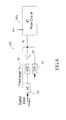
- Figure 8 illustrates a further example of a hybrid driving circuit, which is applicable to the hybrid driving circuit 12 of Figure 1 .
- the hybrid driving circuit 12C of Figure 8 implements voltage programming technique.
- the hybrid driving circuit 13C is a direct digital hybrid driving circuit.
- the direct digital programming circuit 13C includes a microcomputer uC 50 which receives digital data (Vdada), a digital to analog (D/A) converter 52, a voltage follower 54 for increasing current without affecting voltage, and an analog to digital (A/D) converter 56.
- the threshold Vt of the drive TFT may increase slowly. Thus, it may not be necessary to acquire the threshold Vt of the drive TFT every programming cycle. This effectively hides the Vt acquisition for the majority of the programming cycle.
- the threshold Vt acquired from the pixel circuit 10A is digitalized at the A/D converter 56, and is stored in memory contained in the uC 50.
- the digital data that defines the brightness of the pixel is added to the Vt in the uC 50.
- the resulting voltage is then converted back to an analog value at the D/A 52, which is programmed into the pixel circuit 10A.
- This programming method is designed to compensate for the slow process of the Vt acquisition.
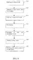
- FIG. 9 illustrates an exemplary flow chart for showing the operation of the hybrid driving circuit 12C of Figure 8 .
- the Vt acquisition mode the Vt is sampled and recorded at step S30.
- writing mode When writing mode is enabled, new data is provided based on the recorded data. It is noted that the operation of the system having the hybrid driving circuit 12C of Figure 8 is not limited to Figure 9 .
- the data which have been recorded may be used without implementing the Vt acquisition.
- Figure 10 illustrates an exemplary timing chart for showing the operation of the hybrid driving circuit 12C of Figure 8 .
- the hybrid driving circuit 13C may use the Vt that has been previously acquired and has been recorded in the uC 50.
- the conversion of the output on the data node DL by A/D can remove the requirements of having to acquire the Vt every programming cycle.
- the Vt of the pixel circuit 10A may be acquired once every second or less. Thus, it may acquire Vt for only one row of the display per frame cycle. This effectively increases the amount of time for the pixel programming cycle. Less frequent need of Vt acquisition ensures faster programming time.
- Figure 2 is used to describe the pixel circuit 10 of Figure 1 .
- the pixel circuit 10 is not limited to that of Figure 2 .
- the pixel circuit 10 may be a pixel circuit illustrated in Figure 11 ( J. Kanichi, J.-H. Kim, J.Y. Nahm, Y. He and R. Hattori "Amorphous Silicon Thin-Film Transistor Based Active-Matrix Organic Light Emitting Display” Asia Display IDW 2001 pp. 315 ).
- the pixel circuit of Figure 11 includes four TFTs 64-70, a capacitor C ST 72 and an OLED 74.
- the TFT 78 is a drive TFT that is connected to the OLED 74 and the capacitor C ST 72.
- the pixel circuit of Figure 11 is selected by Vselect1 and Vselect2, and is programmed by Idata.
- the voltage acquired is a combination of the voltage across the OLED 74 and T3 68.
- the technique compensates the voltage change of both the Vt and the OLED 74.
- Idata of Figure 11 corresponds to the data node DL of Figure 2 .
- Figure 12 illustrates a system for driving an AMOLED display in accordance with a further embodiment of the invention.
- the system 82 of Figure 12 includes a hybrid programming circuit having a correction table 80, a source driver 14 for implementing a voltage-programming scheme and a reference current source 94 for implementing a current-programming scheme.
- the system 82 drives a display having a plurality of pixel circuits using the voltage-programming scheme and the current-programming scheme.
- a hybrid controller 98 is provided to control each component.
- the hybrid controller 98 is placed between the A/D converter 96 and the correction table 80, as an example.
- the hybrid controller 98 is similar to the hybrid controller 16 of Figure 1 .
- the pixel circuit driven by the system 82 may be the pixel circuit 10 of Figure 1 , and may be a current programmed pixel circuit or a voltage programmed pixel circuit.
- the pixel circuit driven by the system 82 may be implemented by Figure 2 or Figure 11 , however, is not limited to those of Figures 2 and 11 .
- the hybrid programming circuit includes a correction calculation module 92 for correcting data from the data source 90 based on the correction table 80 and an A/D converter 96.
- the data corrected by the correction calculation module 92 is applied to the source driver 14.
- the source driver 14 generates Vdata based on the corrected data output from the correction calculation module 92.
- Vdata from the source driver 14 and Idata from the reference current source 94 are supplied to the hybrid driver 12.
- the data source 90 is, for example, but not limited to, a DVD.
- the hybrid driver 12 may be implemented either as a switching matrix, or as the digital programming circuit(s) of Figure 8 , 20 or combination thereof.
- the A/D converter 96 may be the A/D converter 56 of Figure 8 .
- the system 82 may implement the Vt acquisition technique described above using the A/D converter 96 (56).
- the correction table 80 is a lookup table.
- the correction table 80 records the relationship between current required to program the pixel circuit and voltage necessary to obtain that current.
- the correction table 80 is built for every pixel in the entire display.
- the correction table 80 is illustrated separately from the correction calculation module 92. However, the correction table 80 may be included in the correction calculation module 92.
- the operation of the system of Figure 12 has two modes, namely display mode and calibration mode.
- the display mode the data from the data source 90 is corrected using the data in the correction table 80, and is applied to the source driver 14.
- the hybrid driver 12 is not involved in the display mode.
- the calibration mode the current from the reference current source 94 is applied to the pixel circuit, and the voltage associated with the current is read from the pixel circuit. The voltage is converted to a digital data by the A/D converter 96.
- the correction table 80 is updated with the correct value based on the digital data.
- a voltage-programming scheme is implemented.
- the voltage on the data line (e.g. DL of Figure 2 ) of the pixel circuit determines the brightness of the pixels.
- the voltage required to program the pixel circuit is calculated from the pixel brightness to be displayed (from the incoming video information) combined with the current/voltage correction information stored in the correction table 80.
- the information on the correction table 80 is combined with incoming video information to ensure that each pixel will maintain a constant brightness over long-term use.
- the current source 94 is connected to the data input node (DL) of the pixel circuit via the hybrid driver 12.
- Each pixel is programmed through a current-programming scheme (where the level of current on the data line determines the brightness of the pixel), and the voltage required to achieve that current is read by the A/D converter 96.
- the voltage required to program the pixel current is sampled at multiple current points by the A/D converter 96.
- the multiple points may be a subset of the possible current levels (e.g. 256 possible levels for 8-bit, or 64 levels for 6-bit). This subset of voltage measurements is used to construct the correction table 80 that is interpolated from the measurement points.
- the calibration mode may be entered either through user's command or may be combined with the normal display mode so that the calibration takes place during the display refresh period.
- the entire display may be calibrated at once.
- the display may stop showing incoming video information for a short period of time while each pixel was programmed with a current and the voltage recorded.
- a subset of the pixels may be calibrated, such as one pixel every fixed number of frames. This is virtually transparent to the user, and the correction information may still be acquired for each pixel.
- the table lookup technique combines the technique of the current-programming scheme with the technique of the voltage-programming scheme.
- the pixel circuit is programmed with a current through a current-programming scheme. A voltage to maintain that current is read and is stored at a lookup table. The next time that particular level of current is applied to the pixel circuit, instead of programming with a current, the pixel circuit is programmed based on information on the lookup table. Accordingly, it attains the compensation inherent in the current programming scheme while attaining the fast programming time that is only possible with voltage-programming scheme.
- the correction table (lookup table) 80 is used to correct the current/voltage correction information.
- the system 82 of Figure 12 may use the lookup table to correct the Vt shift and the current/voltage correction information at the same time in combination with the hybrid driving circuit of Figure 3 , 6 , 8 or 20 .
- the hybrid controller 98 extracts the Vt shift information by extending the voltage versus current curve to zero current point.
- the Vt shift information is stored in an array of tables (correction table 80) which is applied to incoming display data.
- the uC 50 of Figure 8 or 20 may utilize the lookup table to generate appropriate voltage and program the pixel circuit.
- the hybrid circuits 12A of Figure 3 and 12B of Figure 6 may be integrated into the system of Figure 12 .
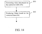
- FIGS 13-14 illustrate exemplary flow charts for showing the operation of the system of Figure 12 .
- calibration mode is enabled.
- a pixel circuit is selected and current programming is implemented to the selected pixel circuit.
- a switch matrix enable signal is enabled. Then the connection to the pixel circuit is changed.
- the Vt is sampled at step s46, and then the correction table is created/corrected at step S48.
- video data are corrected based on the correction table.
- new Vdata is produced based on the corrected data.
- writing mode may be implemented based on the previously created correction table without implementing the calibration mode. It is noted that the operation of the system of Figure 12 is not limited to Figures 13-14 .
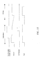
- Figure 15 illustrates an exemplary timing chart for showing a combination of the Vt shift acquisition and the current/voltage correction.
- a switch matrix enable signal in Figure 15 represents a control signal for the hybrid driver 12 of Figure 12 .
- the calibration mode i.e. the current-programming scheme
- the programming mode i.e. the voltage-programming scheme
- the calibration mode may be enabled when the switch matrix enable signal is low.
- the programming mode may be enabled when the switch matrix enable signal is high.
- A/D sampling is implemented during the calibration mode.
- the current from the reference current source 94 is applied to the pixel circuit.
- the voltage on the data input node is converted to a digital voltage by the A/D converter 56.
- current/voltage correction information is recorded at the lookup table.
- the Vt shift information is generated based on the data in the correction table 80 or the output from the A/D converter 96.
- the system 82 of Figure 12 may implement hidden refresh technique for refreshing current/voltage correction information in addition to the table lookup technique described above.
- new current/voltage correction information is constructed while completely hidden from user's perception.
- This technique utilizes the information that is currently displayed on the screen (i.e. the incoming video data).
- the current/voltage correction information for each pixel in the display is known.
- the current/voltage correction curve may shift due to the change in Vt.
- a new current/voltage correction curve is extrapolated from the point so that it is fitted to the measured point. Based on the new current/voltage correction curve, the Vt shift information is extracted which is used to compensate for the shift in Vt.
- Figure 16 illustrates an exemplary flow chart for the hidden refresh operation of the system of Figure 12 .
- a current/voltage correction curve is produced during the calibration process that is implemented during the manufacturing of the display (step S62).
- Figure 17 illustrates an example of a sample of the current voltage correction curve.
- the next step is to measure a point along the curve during the usage of the display.
- This point can be any point along the curve, so any data that the user currently has on the display can be used for calibration (step S64).
- Figure 18 illustrates the current voltage correction of Figure 17 and an example of a newly measured data point.
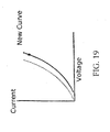
- the last step is to shift the current/voltage correction curve to fit the point of voltage verses current relationship that is measured (step S66).
- Figure 19 illustrates an example of a new current voltage correction curve based on the measured point of Figure 18 .
- the system 82 of Figure 12 may implement a combined current and voltage-programming technique.
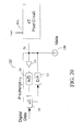
- Figure 20 illustrates one example of a hybrid driving circuit for implementing the combined current and voltage-programming technique.
- the hybrid driving circuit of Figure 20 may be included in the hybrid driver 12 of Figure 12 .
- the digital hybrid driving circuit 12C and a current source 100 are provided to the data line DL of the pixel circuit.
- the pixel circuit programming is divided into two phases.
- the pixel circuit 10A is voltage-programmed first to set the gate voltage of the driving TFT to an approximate value, then followed by a current programming phase.
- the current programming phase can then fine-tune the output current.
- the system of Figure 20 is faster than current programming and has the compensation capabilities of the current programming scheme.
- the digital hybrid driving circuit 12C is provided.
- the combined current and voltage-programming technique may be implemented by combining the hybrid driving circuit 12A of Figure 3 or 12B of Figure 6 with the current source 100.
- the current source 100 may be the reference current source 94 of Figure 12 .
- the system 2 of Figure 1 may implement the hidden refresh technique described above.
- the system 2 of Figure 1 may implement the combined current and voltage-programming technique.
- the system 2 of Figure 1 may include the hybrid driving circuit of Figure 20 to implement the combined current and voltage-programming technique.
- the direct digital programming scheme can be extended to drive an OLED array (e.g. a 4T OLED array) using voltage programmed column drivers, such as those used for driving Active Matrix Liquixd Crystal Display (AMLCD), or voltage-programmed Active-Matrix Organic Light Emitting Diode (AMOLED) displays, or any other voltage-output display driver.
- AMLCD Active Matrix Liquixd Crystal Display
- AMOLED Active-Matrix Organic Light Emitting Diode
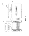
- Figure 21 illustrates a system for driving an AMOLED array having a plurality of pixel circuits in accordance with a further embodiment of the invention.
- the system 105 of Figure 21 includes a voltage column driver 112, a programmable current source 114, a switching network 116, an A/D converter 118 and a row driver 120.
- the voltage column driver 112 is a voltage programmed column driver.
- Each of the voltage column driver 112 and the row driver 120 may be any driver that has a voltage output, such as those designed for the AMLCD.
- the voltage column driver 112 and the programmable current source 114 are connected to an OLED array 110 through the switching network 116.
- the OLED array 110 forms an AMOLED display, and contains a plurality of pixel circuits (such as 10 of Figure 1 ).
- the pixel circuit may be a current programmed pixel circuit or a voltage programmed pixel circuit.
- the A/D converter 118 is an interface that allows an analog signal (i.e. current driving the display 110) to be read back as a digital signal.
- the digital signal associated with the current can than be processed and/or stored.
- the A/D converter 118 may be the A/D converter 56 of Figures 8 and 20 .
- the column driver 112 may be the source driver 14 of Figures 1 and 12 .
- the system 105 of Figure 21 implements the calibration mode and the display mode as described above.
- FIG 22 illustrates an example of the switch network 116 of Figure 21 .
- the switching network 116 of Figure 22 includes two MOSFET switches 122 and 124 that can switch the column of the display (110) from connecting to the column driver (112) to the combination of the current source (114) and the A /D converter (118), and vice versa.
- a shift register 126 is a source of the digital control signal that controls the operation of the MOS switches 122 and 124.
- An inverter 128 inverts an output from the shift register 126. Thus, when the switch 122 is on (off), the switch 124 is off (on).
- the switching network 116 may be located either off the glass in the column driver (112) or directly on the glass using TFT switches.
- the system 105 uses only one current source 114.
- the voltage-programming drivers (such as, AMLCD drivers, or any other voltage-output drivers) drive the rest of the display 110.
- the switching matrix (switching network 116) allows different pixels within the array of pixels to be connected to a single current source (114) through a time division method. This allows a single current source to be applied to the entire display. This lowers the cost of the driver circuit and speeds up the programming time for the pixel circuit.
- the system 105 uses the A/D converter 118 to convert an analog output of the data node (e.g. DL of Figure 2 ) of the pixel circuit to digital data.
- the conversion by the A/D converter 118 removes the requirements of having to acquire the Vt every programming cycle.
- the Vt of the pixel circuit may be acquired once every few minutes. Thus it may acquire one column of the panel every refresh cycle.
- Only one A/D 118 may be implemented for all the columns.
- the circuit acquires only one pixel per frame refresh. For example, for a 320 by 240 panel, the number of pixels is 76, 8000. For a frame rate of 30Hz, the time required to acquire Vt from all pixels for the entire frame is 43 minutes. This may be acceptable for some applications, providing that Vt does not shift substantially in an hour.
- the parasitics only affect the amount of time to discharge the capacitor to acquire Vt. Since the circuit is voltage-programmed, it is not affected by the parasitics. Since Vt is only acquired one column per frame time, it can be long. For example, for a display with 320 columns that has a frame rate of 30Hz, each frame time is 33mS. For voltage programming, it is possible to program a pixel in 70uS. For 320 columns, the time to update the display is 22mS, which still leave 11mS to complete a charge/discharge cycle.
- the system 105 may implement the lookup table technique to compensate for Vt shift and/or to correct the current/voltage information as described above
- the system 105 may implement the hidden refresh technique to acquire the Vt shift information and current/voltage correction information of each pixel circuit (10) in the display 110.
- This current/voltage correction information is used to populate a lookup table (e.g. a correction table 80 of Figure 12 ) that will then be used to compensate for the degradation in the pixel circuit, which is caused by aging.
- a lookup table e.g. a correction table 80 of Figure 12
- the system 105 may implement the combined current and voltage-programming technique as described above.
- Figure 23 illustrates a system for correcting the current/voltage information of the pixel circuit.
- a display 130 is depicted as a 2T or 4T OLED array.
- the display 130 may include a plurality of pixel circuits, each having three or more than four transistors.
- the display 130 may include voltage-driven pixel circuits or current-driven pixel circuits.
- the system of Figure 23 is applicable to the systems 2, 82 and 105 of Figures 1 , 12 and 22 .
- a switch 132 is provided to disconnect the common electrode of the OLED. It is well known that two electrodes are provided for the OLED. One is connected to the pixel circuit, and the other is a common electrode connected to all OLEDs. It is noted that the common electrode may be Vdd or GND depending on the type of OLED.
- the switch 132 connects the common electrode of the OLED into a current sensing network 134 utilizing a high side common mode sensor (such as, INA168 by TI). The current sensing network 134 measures the current through the common electrode.
- each pixel is lit individually and the current consumed is acquired by the sensing network 134.
- the acquired current is used to correct the lookup table (e.g. the correction table 80 of Figure 12 ) populated by the direct digital hybrid driving circuit of Figure 8 or 20 .
- a dark display current may be acquired to include the effect of dead pixel and leakage current of the array. During this procedure, all pixels are turned off, and the current (i.e. dark display current) is measured.
- the major issue with current-programmed pixel circuits which is the slow programming time, is solved.
- the concept of using feedback to compensate the pixel circuit enhances the uniformity and stability of the display while retaining the fast programming capability of the voltage programmed drive scheme.
- system for driving a display which includes a plurality of pixel circuits, each having a plurality of thin film transistors (TFTs) and an organic light emitting diode (OLED), comprising a voltage driver for generating a voltage to program the pixel circuit, a programmable current source for generating a current to program the pixel circuit, and a switching network for selectively connecting the data driver or the current source to one or more pixel circuits.
- TFTs thin film transistors
- OLED organic light emitting diode
- the switching network includes a first switch for connecting the voltage driver to one or more pixel circuits, and a second switch for connecting the current source to one or more pixel circuits.
- the switching network includes a shift register for controlling the operation of the first and second switches.
- a system according to the first aspect, further comprising an analog/digital converter for sampling a voltage on a data node of the pixel circuit.
- a system further comprising a lookup table for storing a current/voltage information representing a relationship between a program current and a program voltage associated with the program current.
- a system according to the fifth aspect, further comprising a current sensing network for sensing a current consumed in the pixel circuit to correct the lookup table.
- a system according to the fifth aspect, further comprising a module for correcting the current/voltage information during the current-based programming or the voltage-based programming.
- a system further comprising a programming circuit for acquiring the threshold voltage of the TFT from the pixel circuit, having an analog to digital converter for converting an analog threshold voltage information to a digital threshold voltage information, and for programming the pixel circuit based on the digital threshold voltage information and the voltage associated with incoming video information.
- a system for driving a pixel circuit having a plurality of thin film transistors (TFTs) and an organic light emitting diode (OLED), comprising a pre-charge controller for pre-charging and discharging a data node of the pixel circuit to acquire threshold voltage information of the TFT from the data node, and a hybrid driving circuit for programming the pixel circuit based on the acquired threshold voltage information and video data information displayed on the pixel circuit.
- TFTs thin film transistors
- OLED organic light emitting diode
- the hybrid driving circuit includes a capacitor coupled to the data node.
- the hybrid driving circuit includes a sampling circuit for sampling the threshold voltage information on the data node, a summer for summing the video data voltage and the sampled voltage threshold information, and a switch for selectively connecting the output of the summer to the data node.
- the hybrid driving circuit includes an analog to digital converter for converting the threshold voltage information to a digital threshold voltage information, a microcomputer for storing the digital threshold voltage information and summing the digital threshold voltage information and the voltage, and a digital to analog converter for converting the summing result output from the microcomputer to an analog data and providing the analog data to the data node.
- a system according to the ninth aspect, further comprising a programming circuit for providing a current on the data node to program the pixel circuit.
- the hybrid driving circuit includes a switching matrix for selecting one of a voltage programming mode and a current programming mode to program the pixel by the selected programming mode.
- a system for driving a pixel circuit having a plurality of thin film transistors (TFTs) and an organic light emitting diode (OLED), comprising a sampler for sampling, from a data node of the pixel circuit, a voltage required to program the pixel circuit, a programming circuit for programming the pixel circuit based on the sampled voltage and video data information displayed on the pixel circuit.
- TFTs thin film transistors
- OLED organic light emitting diode
- a system further comprising a current source for providing current to the pixel circuit during a calibration mode, and a lookup table for storing a current/voltage information representing a relationship between the current and the sampled voltage associated with the current.
- a seventeenth aspect there is provided a system according to the sixteenth aspect, wherein the lookup table is created to each pixel circuit.
- a correction calculation module for correcting data from a data source based on the current/voltage information, during a writing mode, a voltage associated with the corrected data being applied to the pixel circuit.
- a system according to the sixteenth aspect, further comprising a module for extracting a threshold voltage shift of the TFT based on the sampled voltage.
- a system further comprising a lookup table for storing a current/voltage curve representing a relationship between a current and a voltage necessary to program the current into the pixel circuit a module for correcting the current/voltage curve based on the sampled voltage associated with information currently displayed on the pixel circuit, during a writing mode, a voltage to be programmed being determined based on the current/voltage curve.
- a system according to the twentieth aspect wherein the lookup table is created to each pixel circuit.
- a system according to the twentieth aspect further comprising a module for extracting a threshold voltage shift of the TFT based on the corrected current/voltage curve.
- a system according to any one of the first to twenty-second aspects, wherein the system is applicable to a current-programmed pixel circuits and a voltage-programmed pixel circuit.
- the TFT includes amorphous silicon, polysilicon (n-type or p-type), crystalline silicon, or organic based TFT.
- the OLED includes NIP or PIN OLED, and is locatable in the source or the drain of one or more driving TFTs.
- a method of driving a pixel circuit having a plurality of thin film transistors (TFTs) and an organic light emitting diode (OLED), comprising selecting a pixel circuit and pre-charging a data node of the pixel circuit, allowing the pre-charged data node to be discharged, extracting a threshold voltage of the TFT through the discharging step, and programming the pixel circuit, including compensating a programming data based on the extracted threshold voltage.
- TFTs thin film transistors
- OLED organic light emitting diode
- the extracting step includes sampling the threshold voltage, and recording the sampled threshold voltage, the compensating step utilizing the recorded sampled threshold voltage.
- the programming step includes subsequently programming the pixel circuit based on the recorded threshold voltage.
- the programming step includes programming information on the pixel circuit with a current-programming scheme and a voltage-programming scheme.
- a method of driving a pixel circuit having a plurality of thin film transistors (TFTs) and an organic light emitting diode (OLED), comprising sampling, from a data node of the pixel circuit, a voltage required to program the pixel circuit, programming the pixel circuit based on the sampled voltage and information displayed on the pixel circuit.
- TFTs thin film transistors
- OLED organic light emitting diode
- a method further comprising enabling a calibration mode, and implementing a current-programming scheme to the pixel circuit, the sampling step implementing sampling operation during the calibration mode.
- a method further comprising creating, based on the sampling, a lookup table storing a current/voltage correction information representing the current and the sampled voltage associated with the current, the programming step including the step of correcting data from a data source based on the current/voltage correction information.
- a method further comprising storing a current/voltage correction information representing a current and a voltage necessary to program the current into the pixel circuit, and correcting the current/voltage correction information based on the sampled voltage associated with information currently displayed on the pixel circuit.
- a method further comprising sensing a current consumed in the pixel circuit, correcting the current/voltage correction information based on the sensed current.
- a method according to the thirty-third aspect, further comprising sensing a current consumed in the pixel circuit, the correcting step correcting the current/voltage correction information based on the sensed current.
- a hybrid driving circuit for implementing the switching network according to the first aspect, wherein the hybrid driving circuit is applicable to driving scheme, including drive schemes that use timing of the data, select or power inputs to the pixel circuits to achieve increased brightness uniformity, drive schemes that use current voltage feedback, and drive schemes that use optical feedback.
- hybrid driving circuit for implementing the system according to either the ninth or fifteenth aspect, wherein the hybrid driving circuit is applicable to any driving scheme, including drive schemes that use timing of the data, select or power inputs to the pixel circuits to achieve increased brightness uniformity, drive schemes that use current or voltage feedback, and drive schemes that use optical feedback.
- the OLED material includes fluorescent, phosphorescent, polymer, or dendrimer.
Landscapes
- Engineering & Computer Science (AREA)
- Physics & Mathematics (AREA)
- Computer Hardware Design (AREA)
- General Physics & Mathematics (AREA)
- Theoretical Computer Science (AREA)
- Control Of Indicators Other Than Cathode Ray Tubes (AREA)
- Control Of El Displays (AREA)
- Electroluminescent Light Sources (AREA)
Applications Claiming Priority (2)
| Application Number | Priority Date | Filing Date | Title |
|---|---|---|---|
| CA002472671A CA2472671A1 (fr) | 2004-06-29 | 2004-06-29 | Procede de programmation par tensions pour affichages a del excitees par courant |
| EP05759141.4A EP1779365B1 (fr) | 2004-06-29 | 2005-06-28 | Configuration d'une programmation par tension pour ecrans amoled alimentes par courant |
Related Parent Applications (2)
| Application Number | Title | Priority Date | Filing Date |
|---|---|---|---|
| EP05759141.4A Division EP1779365B1 (fr) | 2004-06-29 | 2005-06-28 | Configuration d'une programmation par tension pour ecrans amoled alimentes par courant |
| EP05759141.4A Division-Into EP1779365B1 (fr) | 2004-06-29 | 2005-06-28 | Configuration d'une programmation par tension pour ecrans amoled alimentes par courant |
Publications (2)
| Publication Number | Publication Date |
|---|---|
| EP2827323A2 true EP2827323A2 (fr) | 2015-01-21 |
| EP2827323A3 EP2827323A3 (fr) | 2015-04-08 |
Family
ID=35588998
Family Applications (2)
| Application Number | Title | Priority Date | Filing Date |
|---|---|---|---|
| EP14181848.4A Ceased EP2827323A3 (fr) | 2004-06-29 | 2005-06-28 | Configuration d'une programmation par tension pour écrans amoled alimentés par courant |
| EP05759141.4A Expired - Lifetime EP1779365B1 (fr) | 2004-06-29 | 2005-06-28 | Configuration d'une programmation par tension pour ecrans amoled alimentes par courant |
Family Applications After (1)
| Application Number | Title | Priority Date | Filing Date |
|---|---|---|---|
| EP05759141.4A Expired - Lifetime EP1779365B1 (fr) | 2004-06-29 | 2005-06-28 | Configuration d'une programmation par tension pour ecrans amoled alimentes par courant |
Country Status (7)
| Country | Link |
|---|---|
| US (4) | US8115707B2 (fr) |
| EP (2) | EP2827323A3 (fr) |
| JP (1) | JP5279265B2 (fr) |
| CN (2) | CN102426822B (fr) |
| CA (1) | CA2472671A1 (fr) |
| TW (1) | TW200603057A (fr) |
| WO (1) | WO2006000101A1 (fr) |
Families Citing this family (154)
| Publication number | Priority date | Publication date | Assignee | Title |
|---|---|---|---|---|
| US7569849B2 (en) | 2001-02-16 | 2009-08-04 | Ignis Innovation Inc. | Pixel driver circuit and pixel circuit having the pixel driver circuit |
| CA2419704A1 (fr) | 2003-02-24 | 2004-08-24 | Ignis Innovation Inc. | Methode de fabrication d'un pixel au moyen d'une diode electroluminescente organique |
| CA2443206A1 (fr) | 2003-09-23 | 2005-03-23 | Ignis Innovation Inc. | Panneaux arriere d'ecran amoled - circuits de commande des pixels, architecture de reseau et compensation externe |
| CA2472671A1 (fr) | 2004-06-29 | 2005-12-29 | Ignis Innovation Inc. | Procede de programmation par tensions pour affichages a del excitees par courant |
| CA2490858A1 (fr) | 2004-12-07 | 2006-06-07 | Ignis Innovation Inc. | Methode d'attaque pour la programmation a tension compensee d'affichages del organiques a matrice active |
| US8576217B2 (en) | 2011-05-20 | 2013-11-05 | Ignis Innovation Inc. | System and methods for extraction of threshold and mobility parameters in AMOLED displays |
| US20140111567A1 (en) | 2005-04-12 | 2014-04-24 | Ignis Innovation Inc. | System and method for compensation of non-uniformities in light emitting device displays |
| US8599191B2 (en) | 2011-05-20 | 2013-12-03 | Ignis Innovation Inc. | System and methods for extraction of threshold and mobility parameters in AMOLED displays |
| TWI402790B (zh) | 2004-12-15 | 2013-07-21 | Ignis Innovation Inc | 用以程式化,校準及驅動一發光元件顯示器的方法及系統 |
| US9280933B2 (en) | 2004-12-15 | 2016-03-08 | Ignis Innovation Inc. | System and methods for extraction of threshold and mobility parameters in AMOLED displays |
| US9171500B2 (en) | 2011-05-20 | 2015-10-27 | Ignis Innovation Inc. | System and methods for extraction of parasitic parameters in AMOLED displays |
| US9799246B2 (en) | 2011-05-20 | 2017-10-24 | Ignis Innovation Inc. | System and methods for extraction of threshold and mobility parameters in AMOLED displays |
| US9275579B2 (en) | 2004-12-15 | 2016-03-01 | Ignis Innovation Inc. | System and methods for extraction of threshold and mobility parameters in AMOLED displays |
| US10012678B2 (en) | 2004-12-15 | 2018-07-03 | Ignis Innovation Inc. | Method and system for programming, calibrating and/or compensating, and driving an LED display |
| US10013907B2 (en) | 2004-12-15 | 2018-07-03 | Ignis Innovation Inc. | Method and system for programming, calibrating and/or compensating, and driving an LED display |
| CA2495726A1 (fr) | 2005-01-28 | 2006-07-28 | Ignis Innovation Inc. | Pixel programme par tension a reference locale pour affichages amoled |
| CA2496642A1 (fr) | 2005-02-10 | 2006-08-10 | Ignis Innovation Inc. | Methode d'attaque a courte duree de stabilisation pour afficheurs a diodes organiques electroluminescentes (oled) programmes par courant |
| JP4852866B2 (ja) * | 2005-03-31 | 2012-01-11 | カシオ計算機株式会社 | 表示装置及びその駆動制御方法 |
| US7907137B2 (en) * | 2005-03-31 | 2011-03-15 | Casio Computer Co., Ltd. | Display drive apparatus, display apparatus and drive control method thereof |
| JP4798342B2 (ja) * | 2005-03-31 | 2011-10-19 | カシオ計算機株式会社 | 表示駆動装置及びその駆動制御方法、並びに、表示装置及びその駆動制御方法 |
| JP2006317696A (ja) * | 2005-05-12 | 2006-11-24 | Sony Corp | 画素回路および表示装置、並びに画素回路の制御方法 |
| CN102663977B (zh) | 2005-06-08 | 2015-11-18 | 伊格尼斯创新有限公司 | 用于驱动发光器件显示器的方法和系统 |
| CA2510855A1 (fr) | 2005-07-06 | 2007-01-06 | Ignis Innovation Inc. | Methode de commande rapide d'affichages amoled |
| KR100703463B1 (ko) | 2005-08-01 | 2007-04-03 | 삼성에스디아이 주식회사 | 데이터 구동회로와 이를 이용한 유기 발광 표시장치 및그의 구동방법 |
| CA2518276A1 (fr) | 2005-09-13 | 2007-03-13 | Ignis Innovation Inc. | Technique de compensation de la degradation de luminance dans des dispositifs electroluminescents |
| US9269322B2 (en) | 2006-01-09 | 2016-02-23 | Ignis Innovation Inc. | Method and system for driving an active matrix display circuit |
| US9489891B2 (en) | 2006-01-09 | 2016-11-08 | Ignis Innovation Inc. | Method and system for driving an active matrix display circuit |
| WO2007079572A1 (fr) | 2006-01-09 | 2007-07-19 | Ignis Innovation Inc. | Procédé et système pour entraîner un circuit d’affichage de matrice active |
| US7924249B2 (en) | 2006-02-10 | 2011-04-12 | Ignis Innovation Inc. | Method and system for light emitting device displays |
| CN101501748B (zh) | 2006-04-19 | 2012-12-05 | 伊格尼斯创新有限公司 | 有源矩阵显示器的稳定驱动设计 |
| TWI385621B (zh) * | 2006-08-01 | 2013-02-11 | Casio Computer Co Ltd | 顯示驅動裝置及其驅動方法、以及顯示裝置及其驅動方法 |
| JP4935979B2 (ja) * | 2006-08-10 | 2012-05-23 | カシオ計算機株式会社 | 表示装置及びその駆動方法、並びに、表示駆動装置及びその駆動方法 |
| US8199074B2 (en) * | 2006-08-11 | 2012-06-12 | Chimei Innolux Corporation | System and method for reducing mura defects |
| CA2556961A1 (fr) | 2006-08-15 | 2008-02-15 | Ignis Innovation Inc. | Technique de compensation de diodes electroluminescentes organiques basee sur leur capacite |
| JP5240542B2 (ja) * | 2006-09-25 | 2013-07-17 | カシオ計算機株式会社 | 表示駆動装置及びその駆動方法、並びに、表示装置及びその駆動方法 |
| JP4222426B2 (ja) | 2006-09-26 | 2009-02-12 | カシオ計算機株式会社 | 表示駆動装置及びその駆動方法、並びに、表示装置及びその駆動方法 |
| JP2008292834A (ja) * | 2007-05-25 | 2008-12-04 | Hitachi Displays Ltd | 表示装置 |
| US8405585B2 (en) * | 2008-01-04 | 2013-03-26 | Chimei Innolux Corporation | OLED display, information device, and method for displaying an image in OLED display |
| JP4715850B2 (ja) * | 2008-01-15 | 2011-07-06 | ソニー株式会社 | 表示装置及びその駆動方法と電子機器 |
| KR100969769B1 (ko) * | 2008-01-21 | 2010-07-13 | 삼성모바일디스플레이주식회사 | 유기전계발광 표시장치 및 그의 구동방법 |
| TW200949807A (en) | 2008-04-18 | 2009-12-01 | Ignis Innovation Inc | System and driving method for light emitting device display |
| CN101285848B (zh) * | 2008-05-28 | 2010-06-02 | 炬力集成电路设计有限公司 | 一种校正和获取参考电压的方法和装置 |
| CA2637343A1 (fr) | 2008-07-29 | 2010-01-29 | Ignis Innovation Inc. | Amelioration de pilote de source d'affichage |
| US9370075B2 (en) | 2008-12-09 | 2016-06-14 | Ignis Innovation Inc. | System and method for fast compensation programming of pixels in a display |
| JP5239812B2 (ja) * | 2008-12-11 | 2013-07-17 | ソニー株式会社 | 表示装置、表示装置の駆動方法および電子機器 |
| CA2669367A1 (fr) | 2009-06-16 | 2010-12-16 | Ignis Innovation Inc | Technique de compensation pour la variation chromatique des ecrans d'affichage . |
| US9384698B2 (en) | 2009-11-30 | 2016-07-05 | Ignis Innovation Inc. | System and methods for aging compensation in AMOLED displays |
| US10319307B2 (en) | 2009-06-16 | 2019-06-11 | Ignis Innovation Inc. | Display system with compensation techniques and/or shared level resources |
| US9311859B2 (en) | 2009-11-30 | 2016-04-12 | Ignis Innovation Inc. | Resetting cycle for aging compensation in AMOLED displays |
| CA2688870A1 (fr) | 2009-11-30 | 2011-05-30 | Ignis Innovation Inc. | Procede et techniques pour ameliorer l'uniformite d'affichage |
| US8379012B2 (en) * | 2009-07-17 | 2013-02-19 | Atmel Corporation | Selector switch for direct connection of switched regulator to voltage inputs |
| JP5503255B2 (ja) | 2009-11-10 | 2014-05-28 | グローバル・オーエルイーディー・テクノロジー・リミテッド・ライアビリティ・カンパニー | 画素回路、表示装置および検査方法 |
| US8633873B2 (en) | 2009-11-12 | 2014-01-21 | Ignis Innovation Inc. | Stable fast programming scheme for displays |
| US10996258B2 (en) | 2009-11-30 | 2021-05-04 | Ignis Innovation Inc. | Defect detection and correction of pixel circuits for AMOLED displays |
| US8803417B2 (en) | 2009-12-01 | 2014-08-12 | Ignis Innovation Inc. | High resolution pixel architecture |
| CA2686174A1 (fr) | 2009-12-01 | 2011-06-01 | Ignis Innovation Inc | Architecture de pixels haute resolution |
| CA2687631A1 (fr) | 2009-12-06 | 2011-06-06 | Ignis Innovation Inc | Mecanisme de commande a faible puissance pour applications d'affichage |
| US10163401B2 (en) | 2010-02-04 | 2018-12-25 | Ignis Innovation Inc. | System and methods for extracting correlation curves for an organic light emitting device |
| US9881532B2 (en) | 2010-02-04 | 2018-01-30 | Ignis Innovation Inc. | System and method for extracting correlation curves for an organic light emitting device |
| US20140313111A1 (en) | 2010-02-04 | 2014-10-23 | Ignis Innovation Inc. | System and methods for extracting correlation curves for an organic light emitting device |
| US10176736B2 (en) | 2010-02-04 | 2019-01-08 | Ignis Innovation Inc. | System and methods for extracting correlation curves for an organic light emitting device |
| US10089921B2 (en) | 2010-02-04 | 2018-10-02 | Ignis Innovation Inc. | System and methods for extracting correlation curves for an organic light emitting device |
| CA2692097A1 (fr) | 2010-02-04 | 2011-08-04 | Ignis Innovation Inc. | Extraction de courbes de correlation pour des dispositifs luminescents |
| CA2696778A1 (fr) | 2010-03-17 | 2011-09-17 | Ignis Innovation Inc. | Procedes d'extraction des parametres d'uniformite de duree de vie |
| DE102010019667B4 (de) * | 2010-04-28 | 2014-02-20 | Fraunhofer-Gesellschaft zur Förderung der angewandten Forschung e.V. | Schaltungsanordnung für in einer zweidimensionalen Matrix angeordnete organische Leuchtdioden |
| KR101101554B1 (ko) * | 2010-08-19 | 2012-01-02 | 한국과학기술원 | 액티브 유기 발광 표시장치 |
| US8907991B2 (en) | 2010-12-02 | 2014-12-09 | Ignis Innovation Inc. | System and methods for thermal compensation in AMOLED displays |
| JP5182382B2 (ja) * | 2011-01-11 | 2013-04-17 | カシオ計算機株式会社 | 表示装置 |
| JP5182383B2 (ja) * | 2011-01-11 | 2013-04-17 | カシオ計算機株式会社 | 表示装置 |
| US9351368B2 (en) | 2013-03-08 | 2016-05-24 | Ignis Innovation Inc. | Pixel circuits for AMOLED displays |
| US9886899B2 (en) | 2011-05-17 | 2018-02-06 | Ignis Innovation Inc. | Pixel Circuits for AMOLED displays |
| WO2012156942A1 (fr) | 2011-05-17 | 2012-11-22 | Ignis Innovation Inc. | Systèmes et procédés pour systèmes d'affichage comprenant une commande de puissance dynamique |
| US9606607B2 (en) | 2011-05-17 | 2017-03-28 | Ignis Innovation Inc. | Systems and methods for display systems with dynamic power control |
| US20140368491A1 (en) | 2013-03-08 | 2014-12-18 | Ignis Innovation Inc. | Pixel circuits for amoled displays |
| US9530349B2 (en) | 2011-05-20 | 2016-12-27 | Ignis Innovations Inc. | Charged-based compensation and parameter extraction in AMOLED displays |
| US9466240B2 (en) | 2011-05-26 | 2016-10-11 | Ignis Innovation Inc. | Adaptive feedback system for compensating for aging pixel areas with enhanced estimation speed |
| US9773439B2 (en) | 2011-05-27 | 2017-09-26 | Ignis Innovation Inc. | Systems and methods for aging compensation in AMOLED displays |
| EP2715711A4 (fr) | 2011-05-28 | 2014-12-24 | Ignis Innovation Inc | Système et procédé de programmation de compensation rapide de pixels dans un écran d'affichage |
| US9070775B2 (en) | 2011-08-03 | 2015-06-30 | Ignis Innovations Inc. | Thin film transistor |
| US8901579B2 (en) | 2011-08-03 | 2014-12-02 | Ignis Innovation Inc. | Organic light emitting diode and method of manufacturing |
| GB2495117A (en) * | 2011-09-29 | 2013-04-03 | Cambridge Display Tech Ltd | Display driver circuits for OLED displays |
| KR101536129B1 (ko) * | 2011-10-04 | 2015-07-14 | 엘지디스플레이 주식회사 | 유기발광 표시장치 |
| KR101463651B1 (ko) * | 2011-10-12 | 2014-11-20 | 엘지디스플레이 주식회사 | 유기발광 표시장치 |
| CN102708788B (zh) * | 2011-11-23 | 2015-01-07 | 京东方科技集团股份有限公司 | 像素电路 |
| US10089924B2 (en) | 2011-11-29 | 2018-10-02 | Ignis Innovation Inc. | Structural and low-frequency non-uniformity compensation |
| US9385169B2 (en) | 2011-11-29 | 2016-07-05 | Ignis Innovation Inc. | Multi-functional active matrix organic light-emitting diode display |
| US9324268B2 (en) | 2013-03-15 | 2016-04-26 | Ignis Innovation Inc. | Amoled displays with multiple readout circuits |
| KR101362002B1 (ko) | 2011-12-12 | 2014-02-11 | 엘지디스플레이 주식회사 | 유기발광 표시장치 |
| US8937632B2 (en) | 2012-02-03 | 2015-01-20 | Ignis Innovation Inc. | Driving system for active-matrix displays |
| US9190456B2 (en) | 2012-04-25 | 2015-11-17 | Ignis Innovation Inc. | High resolution display panel with emissive organic layers emitting light of different colors |
| US9747834B2 (en) | 2012-05-11 | 2017-08-29 | Ignis Innovation Inc. | Pixel circuits including feedback capacitors and reset capacitors, and display systems therefore |
| US8922544B2 (en) | 2012-05-23 | 2014-12-30 | Ignis Innovation Inc. | Display systems with compensation for line propagation delay |
| KR101528148B1 (ko) | 2012-07-19 | 2015-06-12 | 엘지디스플레이 주식회사 | 화소 전류 측정을 위한 유기 발광 다이오드 표시 장치 및 그의 화소 전류 측정 방법 |
| US9786223B2 (en) | 2012-12-11 | 2017-10-10 | Ignis Innovation Inc. | Pixel circuits for AMOLED displays |
| US9336717B2 (en) | 2012-12-11 | 2016-05-10 | Ignis Innovation Inc. | Pixel circuits for AMOLED displays |
| US9171504B2 (en) | 2013-01-14 | 2015-10-27 | Ignis Innovation Inc. | Driving scheme for emissive displays providing compensation for driving transistor variations |
| US9830857B2 (en) | 2013-01-14 | 2017-11-28 | Ignis Innovation Inc. | Cleaning common unwanted signals from pixel measurements in emissive displays |
| US9721505B2 (en) | 2013-03-08 | 2017-08-01 | Ignis Innovation Inc. | Pixel circuits for AMOLED displays |
| CA2894717A1 (fr) | 2015-06-19 | 2016-12-19 | Ignis Innovation Inc. | Caracterisation d'un dispositif optoelectronique au moyen d'une ligne de sens partage |
| EP3043338A1 (fr) | 2013-03-14 | 2016-07-13 | Ignis Innovation Inc. | Re-interpolation avec détection de bord pour extraire un motif de vieillissement d'écrans amoled |
| WO2014140992A1 (fr) | 2013-03-15 | 2014-09-18 | Ignis Innovation Inc. | Réglage dynamique des résolutions tactiles d'un écran amoled |
| CN105144361B (zh) | 2013-04-22 | 2019-09-27 | 伊格尼斯创新公司 | 用于oled显示面板的检测系统 |
| TWI497472B (zh) | 2013-06-06 | 2015-08-21 | Au Optronics Corp | 顯示器之畫素驅動方法及其顯示器 |
| DE112014003719T5 (de) | 2013-08-12 | 2016-05-19 | Ignis Innovation Inc. | Kompensationsgenauigkeit |
| TW201508908A (zh) | 2013-08-19 | 2015-03-01 | Chunghwa Picture Tubes Ltd | 有機發光二極體的畫素電路 |
| KR102071690B1 (ko) | 2013-08-19 | 2020-01-31 | 삼성디스플레이 주식회사 | 노이즈 제거 회로 및 이를 포함하는 전류 센싱부 |
| KR102058577B1 (ko) | 2013-09-13 | 2019-12-24 | 삼성디스플레이 주식회사 | 표시 장치 및 그 구동 방법 |
| KR102084711B1 (ko) | 2013-10-10 | 2020-04-16 | 삼성디스플레이 주식회사 | 표시 장치 및 표시 장치 구동방법 |
| KR102109191B1 (ko) | 2013-11-14 | 2020-05-12 | 삼성디스플레이 주식회사 | 유기전계발광 표시장치 및 그의 구동방법 |
| KR102212424B1 (ko) | 2013-11-18 | 2021-02-04 | 삼성디스플레이 주식회사 | 표시 장치 및 표시 장치 구동방법 |
| US9443469B2 (en) | 2013-11-22 | 2016-09-13 | Global Oled Technology Llc | Pixel circuit, driving method, display device, and inspection method |
| US9741282B2 (en) | 2013-12-06 | 2017-08-22 | Ignis Innovation Inc. | OLED display system and method |
| US9761170B2 (en) | 2013-12-06 | 2017-09-12 | Ignis Innovation Inc. | Correction for localized phenomena in an image array |
| US9502653B2 (en) | 2013-12-25 | 2016-11-22 | Ignis Innovation Inc. | Electrode contacts |
| US10997901B2 (en) | 2014-02-28 | 2021-05-04 | Ignis Innovation Inc. | Display system |
| US10176752B2 (en) | 2014-03-24 | 2019-01-08 | Ignis Innovation Inc. | Integrated gate driver |
| DE102015206281A1 (de) | 2014-04-08 | 2015-10-08 | Ignis Innovation Inc. | Anzeigesystem mit gemeinsam genutzten Niveauressourcen für tragbare Vorrichtungen |
| TWI553609B (zh) | 2014-08-26 | 2016-10-11 | 友達光電股份有限公司 | 顯示裝置及其驅動方法 |
| KR102256069B1 (ko) | 2014-09-03 | 2021-05-25 | 삼성디스플레이 주식회사 | 표시 장치 및 그 보상 방법 |
| KR102270460B1 (ko) | 2014-09-19 | 2021-06-29 | 삼성디스플레이 주식회사 | 유기 발광 표시 장치 및 이의 열화 보상 방법 |
| CA2872563A1 (fr) | 2014-11-28 | 2016-05-28 | Ignis Innovation Inc. | Architecture de reseau a densite de pixels elevee |
| KR102320316B1 (ko) | 2014-12-01 | 2021-11-02 | 삼성디스플레이 주식회사 | 유기 발광 표시 장치 및 이의 구동방법 |
| KR102320300B1 (ko) | 2014-12-01 | 2021-11-03 | 삼성디스플레이 주식회사 | 유기 발광 표시 장치 |
| CA2873476A1 (fr) | 2014-12-08 | 2016-06-08 | Ignis Innovation Inc. | Architecture d'affichage de pixels intelligents |
| CA2879462A1 (fr) | 2015-01-23 | 2016-07-23 | Ignis Innovation Inc. | Compensation de la variation de couleur dans les dispositifs emetteurs |
| CA2886862A1 (fr) | 2015-04-01 | 2016-10-01 | Ignis Innovation Inc. | Ajustement de la luminosite d'affichage en vue d'eviter la surchauffe ou le vieillissement accelere |
| CA2889870A1 (fr) | 2015-05-04 | 2016-11-04 | Ignis Innovation Inc. | Systeme de retroaction optique |
| CA2892714A1 (fr) | 2015-05-27 | 2016-11-27 | Ignis Innovation Inc | Reduction de largeur de bande de memoire dans un systeme de compensation |
| US10657895B2 (en) | 2015-07-24 | 2020-05-19 | Ignis Innovation Inc. | Pixels and reference circuits and timing techniques |
| CA2898282A1 (fr) | 2015-07-24 | 2017-01-24 | Ignis Innovation Inc. | Etalonnage hybride de sources de courant destine a des afficheurs a tension polarisee par courant programmes |
| US10373554B2 (en) | 2015-07-24 | 2019-08-06 | Ignis Innovation Inc. | Pixels and reference circuits and timing techniques |
| KR102435923B1 (ko) | 2015-08-05 | 2022-08-25 | 삼성디스플레이 주식회사 | 유기 발광 표시 장치 및 이의 구동 방법 |
| CA2900170A1 (fr) | 2015-08-07 | 2017-02-07 | Gholamreza Chaji | Etalonnage de pixel fonde sur des valeurs de reference ameliorees |
| CA2908285A1 (fr) | 2015-10-14 | 2017-04-14 | Ignis Innovation Inc. | Pilote comportant une structure de pixel a plusieurs couleurs |
| CA2909813A1 (fr) | 2015-10-26 | 2017-04-26 | Ignis Innovation Inc | Orientation de motif ppi dense |
| FR3047340B1 (fr) | 2016-02-02 | 2019-10-18 | Dassault Aviation | Systeme d'aide a la decision d'autorisation a partir d'un aeronef, et procede associe |
| US9961178B2 (en) * | 2016-03-24 | 2018-05-01 | Motorola Mobility Llc | Embedded active matrix organic light emitting diode (AMOLED) fingerprint sensor |
| TWI587265B (zh) * | 2016-05-31 | 2017-06-11 | 瑞鼎科技股份有限公司 | 顯示驅動裝置 |
| US9875797B1 (en) * | 2016-12-04 | 2018-01-23 | Alex Diggins | Photon memory system |
| US10586491B2 (en) | 2016-12-06 | 2020-03-10 | Ignis Innovation Inc. | Pixel circuits for mitigation of hysteresis |
| US10714018B2 (en) | 2017-05-17 | 2020-07-14 | Ignis Innovation Inc. | System and method for loading image correction data for displays |
| US11025899B2 (en) | 2017-08-11 | 2021-06-01 | Ignis Innovation Inc. | Optical correction systems and methods for correcting non-uniformity of emissive display devices |
| CN107622754B (zh) * | 2017-09-22 | 2023-11-14 | 京东方科技集团股份有限公司 | 像素电路及其控制方法、显示基板、显示装置 |
| CN107516483B (zh) * | 2017-09-28 | 2020-06-30 | 京东方科技集团股份有限公司 | 器件故障的电学检测方法、装置和显示模组 |
| US10971078B2 (en) | 2018-02-12 | 2021-04-06 | Ignis Innovation Inc. | Pixel measurement through data line |
| DE102019210555A1 (de) * | 2018-07-19 | 2020-01-23 | Ignis Innovation Inc. | Systeme und Verfahren zum Kompensieren einer Degradation eines OLED-Displays |
| US11276348B2 (en) * | 2018-07-19 | 2022-03-15 | Ignis Innovation Inc. | Compensation systems and methods for OLED display degradation |
| CN111710304B (zh) * | 2020-07-17 | 2021-12-07 | 京东方科技集团股份有限公司 | 像素驱动电路及其驱动方法、显示设备 |
| WO2022040879A1 (fr) * | 2020-08-24 | 2022-03-03 | 华为技术有限公司 | Circuit d'attaque de pixel et panneau d'affichage à micro-diodes électroluminescentes |
| KR20230142020A (ko) | 2022-03-30 | 2023-10-11 | 삼성디스플레이 주식회사 | 발광 표시 장치 |
| CN114677966B (zh) * | 2022-04-19 | 2024-09-24 | 中南大学 | 一种Micro-LED显示设备及其反馈补偿电路 |
| EP4495924A4 (fr) | 2022-04-20 | 2025-05-21 | Samsung Electronics Co., Ltd | Dispositif électronique et procédé de permutation de tension gamma pour la décharge de pixels |
| US12315432B2 (en) | 2022-06-30 | 2025-05-27 | Boe Technology Group Co., Ltd. | Splicing display screen and display method thereof |
| CN115171607B (zh) | 2022-09-06 | 2023-01-31 | 惠科股份有限公司 | 像素电路、显示面板及显示装置 |
Citations (5)
| Publication number | Priority date | Publication date | Assignee | Title |
|---|---|---|---|---|
| US20010024186A1 (en) * | 1997-09-29 | 2001-09-27 | Sarnoff Corporation | Active matrix light emitting diode pixel structure and concomitant method |
| US20030071821A1 (en) * | 2001-10-11 | 2003-04-17 | Sundahl Robert C. | Luminance compensation for emissive displays |
| US20030095087A1 (en) * | 2001-11-20 | 2003-05-22 | International Business Machines Corporation | Data voltage current drive amoled pixel circuit |
| US6577302B2 (en) * | 2000-03-31 | 2003-06-10 | Koninklijke Philips Electronics N.V. | Display device having current-addressed pixels |
| FR2843225A1 (fr) * | 2002-07-30 | 2004-02-06 | Thomson Licensing Sa | Dispositif de visualisation d'images a matrice active et a compensation de seuil de declenchement |
Family Cites Families (585)
| Publication number | Priority date | Publication date | Assignee | Title |
|---|---|---|---|---|
| US3506851A (en) | 1966-12-14 | 1970-04-14 | North American Rockwell | Field effect transistor driver using capacitor feedback |
| US3774055A (en) | 1972-01-24 | 1973-11-20 | Nat Semiconductor Corp | Clocked bootstrap inverter circuit |
| JPS52119160A (en) | 1976-03-31 | 1977-10-06 | Nec Corp | Semiconductor circuit with insulating gate type field dffect transisto r |
| US4160934A (en) | 1977-08-11 | 1979-07-10 | Bell Telephone Laboratories, Incorporated | Current control circuit for light emitting diode |
| US4354162A (en) | 1981-02-09 | 1982-10-12 | National Semiconductor Corporation | Wide dynamic range control amplifier with offset correction |
| JPS60218626A (ja) | 1984-04-13 | 1985-11-01 | Sharp Corp | カラ−液晶表示装置 |
| JPS61110198A (ja) | 1984-11-05 | 1986-05-28 | 株式会社東芝 | マトリクス形表示装置 |
| JPS61161093A (ja) | 1985-01-09 | 1986-07-21 | Sony Corp | ダイナミツクユニフオミテイ補正装置 |
| KR900009055B1 (ko) | 1986-05-13 | 1990-12-17 | 상요덴기 가부시기가이샤 | 영상 표시 장치용 구동 회로 |
| JP2623087B2 (ja) | 1986-09-27 | 1997-06-25 | 潤一 西澤 | カラーディスプレー装置 |
| US6323832B1 (en) | 1986-09-27 | 2001-11-27 | Junichi Nishizawa | Color display device |
| US4975691A (en) | 1987-06-16 | 1990-12-04 | Interstate Electronics Corporation | Scan inversion symmetric drive |
| JPH0442619Y2 (fr) | 1987-07-10 | 1992-10-08 | ||
| US4963860A (en) | 1988-02-01 | 1990-10-16 | General Electric Company | Integrated matrix display circuitry |
| JPH01272298A (ja) | 1988-04-25 | 1989-10-31 | Yamaha Corp | 駆動装置 |
| DE68925434T2 (de) | 1988-04-25 | 1996-11-14 | Yamaha Corp | Elektroakustische Antriebsschaltung |
| US4996523A (en) | 1988-10-20 | 1991-02-26 | Eastman Kodak Company | Electroluminescent storage display with improved intensity driver circuits |
| US5198803A (en) | 1990-06-06 | 1993-03-30 | Opto Tech Corporation | Large scale movie display system with multiple gray levels |
| JP3039791B2 (ja) | 1990-06-08 | 2000-05-08 | 富士通株式会社 | Daコンバータ |
| EP0462333B1 (fr) | 1990-06-11 | 1994-08-31 | International Business Machines Corporation | Système d'affichage |
| JPH04158570A (ja) | 1990-10-22 | 1992-06-01 | Seiko Epson Corp | 半導体装置の構造及びその製造方法 |
| US5153420A (en) | 1990-11-28 | 1992-10-06 | Xerox Corporation | Timing independent pixel-scale light sensing apparatus |
| US5204661A (en) | 1990-12-13 | 1993-04-20 | Xerox Corporation | Input/output pixel circuit and array of such circuits |
| US5222082A (en) | 1991-02-28 | 1993-06-22 | Thomson Consumer Electronics, S.A. | Shift register useful as a select line scanner for liquid crystal display |
| JP3163637B2 (ja) | 1991-03-19 | 2001-05-08 | 株式会社日立製作所 | 液晶表示装置の駆動方法 |
| US5280280A (en) | 1991-05-24 | 1994-01-18 | Robert Hotto | DC integrating display driver employing pixel status memories |
| US5489918A (en) | 1991-06-14 | 1996-02-06 | Rockwell International Corporation | Method and apparatus for dynamically and adjustably generating active matrix liquid crystal display gray level voltages |
| US5206633A (en) * | 1991-08-19 | 1993-04-27 | International Business Machines Corp. | Self calibrating brightness controls for digitally operated liquid crystal display system |
| US5589847A (en) | 1991-09-23 | 1996-12-31 | Xerox Corporation | Switched capacitor analog circuits using polysilicon thin film technology |
| US5266515A (en) | 1992-03-02 | 1993-11-30 | Motorola, Inc. | Fabricating dual gate thin film transistors |
| US5572444A (en) | 1992-08-19 | 1996-11-05 | Mtl Systems, Inc. | Method and apparatus for automatic performance evaluation of electronic display devices |
| SG49735A1 (en) | 1993-04-05 | 1998-06-15 | Cirrus Logic Inc | System for compensating crosstalk in LCDS |
| JPH06314977A (ja) | 1993-04-28 | 1994-11-08 | Nec Ic Microcomput Syst Ltd | 電流出力型デジタル/アナログ変換回路 |
| JPH06347753A (ja) | 1993-04-30 | 1994-12-22 | Prime View Hk Ltd | アモルファス・シリコン薄膜トランジスタ装置の閾値電圧を回復するための方法と装置 |
| JPH0799321A (ja) | 1993-05-27 | 1995-04-11 | Sony Corp | 薄膜半導体素子の製造方法および製造装置 |
| JPH07120722A (ja) | 1993-06-30 | 1995-05-12 | Sharp Corp | 液晶表示素子およびその駆動方法 |
| US5712653A (en) | 1993-12-27 | 1998-01-27 | Sharp Kabushiki Kaisha | Image display scanning circuit with outputs from sequentially switched pulse signals |
| JP3067949B2 (ja) | 1994-06-15 | 2000-07-24 | シャープ株式会社 | 電子装置および液晶表示装置 |
| JPH0830231A (ja) | 1994-07-18 | 1996-02-02 | Toshiba Corp | Ledドットマトリクス表示器及びその調光方法 |
| US5714968A (en) | 1994-08-09 | 1998-02-03 | Nec Corporation | Current-dependent light-emitting element drive circuit for use in active matrix display device |
| US6476798B1 (en) | 1994-08-22 | 2002-11-05 | International Game Technology | Reduced noise touch screen apparatus and method |
| US5747928A (en) | 1994-10-07 | 1998-05-05 | Iowa State University Research Foundation, Inc. | Flexible panel display having thin film transistors driving polymer light-emitting diodes |
| US5498880A (en) | 1995-01-12 | 1996-03-12 | E. I. Du Pont De Nemours And Company | Image capture panel using a solid state device |
| US5686935A (en) | 1995-03-06 | 1997-11-11 | Thomson Consumer Electronics, S.A. | Data line drivers with column initialization transistor |
| US5745660A (en) | 1995-04-26 | 1998-04-28 | Polaroid Corporation | Image rendering system and method for generating stochastic threshold arrays for use therewith |
| US5619033A (en) | 1995-06-07 | 1997-04-08 | Xerox Corporation | Layered solid state photodiode sensor array |
| JPH08340243A (ja) | 1995-06-14 | 1996-12-24 | Canon Inc | バイアス回路 |
| US5748160A (en) | 1995-08-21 | 1998-05-05 | Mororola, Inc. | Active driven LED matrices |
| JP3272209B2 (ja) | 1995-09-07 | 2002-04-08 | アルプス電気株式会社 | Lcd駆動回路 |
| JPH0990405A (ja) | 1995-09-21 | 1997-04-04 | Sharp Corp | 薄膜トランジスタ |
| US5945972A (en) | 1995-11-30 | 1999-08-31 | Kabushiki Kaisha Toshiba | Display device |
| JPH09179525A (ja) | 1995-12-26 | 1997-07-11 | Pioneer Electron Corp | 容量性発光素子の駆動方法及び駆動装置 |
| US5790234A (en) | 1995-12-27 | 1998-08-04 | Canon Kabushiki Kaisha | Eyeball detection apparatus |
| US5923794A (en) | 1996-02-06 | 1999-07-13 | Polaroid Corporation | Current-mediated active-pixel image sensing device with current reset |
| US5949398A (en) | 1996-04-12 | 1999-09-07 | Thomson Multimedia S.A. | Select line driver for a display matrix with toggling backplane |
| US6271825B1 (en) | 1996-04-23 | 2001-08-07 | Rainbow Displays, Inc. | Correction methods for brightness in electronic display |
| US5723950A (en) | 1996-06-10 | 1998-03-03 | Motorola | Pre-charge driver for light emitting devices and method |
| JP3266177B2 (ja) | 1996-09-04 | 2002-03-18 | 住友電気工業株式会社 | 電流ミラー回路とそれを用いた基準電圧発生回路及び発光素子駆動回路 |
| US5952991A (en) | 1996-11-14 | 1999-09-14 | Kabushiki Kaisha Toshiba | Liquid crystal display |
| JP3027126B2 (ja) | 1996-11-26 | 2000-03-27 | 松下電器産業株式会社 | 液晶表示装置 |
| US6261009B1 (en) | 1996-11-27 | 2001-07-17 | Zih Corporation | Thermal printer |
| US6046716A (en) | 1996-12-19 | 2000-04-04 | Colorado Microdisplay, Inc. | Display system having electrode modulation to alter a state of an electro-optic layer |
| US5874803A (en) | 1997-09-09 | 1999-02-23 | The Trustees Of Princeton University | Light emitting device with stack of OLEDS and phosphor downconverter |
| JPH10209854A (ja) | 1997-01-23 | 1998-08-07 | Mitsubishi Electric Corp | ボディ電圧制御型半導体集積回路 |
| TW441136B (en) | 1997-01-28 | 2001-06-16 | Casio Computer Co Ltd | An electroluminescent display device and a driving method thereof |
| US5917280A (en) | 1997-02-03 | 1999-06-29 | The Trustees Of Princeton University | Stacked organic light emitting devices |
| EP1830344B1 (fr) | 1997-02-17 | 2012-07-04 | Seiko Epson Corporation | Structure d'un circuit de commande d'élément d'image pour un dispositif d'affichage luminescent |
| JPH10254410A (ja) | 1997-03-12 | 1998-09-25 | Pioneer Electron Corp | 有機エレクトロルミネッセンス表示装置及びその駆動方法 |
| DE69825402T2 (de) * | 1997-03-12 | 2005-08-04 | Seiko Epson Corp. | Pixelschaltung, anzeigevorrichtung und elektronische apparatur mit stromgesteuerter lichtemittierender vorrichtung |
| US5903248A (en) | 1997-04-11 | 1999-05-11 | Spatialight, Inc. | Active matrix display having pixel driving circuits with integrated charge pumps |
| US5952789A (en) | 1997-04-14 | 1999-09-14 | Sarnoff Corporation | Active matrix organic light emitting diode (amoled) display pixel structure and data load/illuminate circuit therefor |
| WO1998048403A1 (fr) | 1997-04-23 | 1998-10-29 | Sarnoff Corporation | Structure de pixel a diode luminescente a matrice active et procede |
| US6229506B1 (en) | 1997-04-23 | 2001-05-08 | Sarnoff Corporation | Active matrix light emitting diode pixel structure and concomitant method |
| US5815303A (en) | 1997-06-26 | 1998-09-29 | Xerox Corporation | Fault tolerant projective display having redundant light modulators |
| US6023259A (en) | 1997-07-11 | 2000-02-08 | Fed Corporation | OLED active matrix using a single transistor current mode pixel design |
| KR100242244B1 (ko) | 1997-08-09 | 2000-02-01 | 구본준 | 스캐닝 회로 |
| KR100323441B1 (ko) | 1997-08-20 | 2002-06-20 | 윤종용 | 엠펙2동화상부호화/복호화시스템 |
| JP3580092B2 (ja) | 1997-08-21 | 2004-10-20 | セイコーエプソン株式会社 | アクティブマトリクス型表示装置 |
| US20010043173A1 (en) | 1997-09-04 | 2001-11-22 | Ronald Roy Troutman | Field sequential gray in active matrix led display using complementary transistor pixel circuits |
| JPH1187720A (ja) | 1997-09-08 | 1999-03-30 | Sanyo Electric Co Ltd | 半導体装置及び液晶表示装置 |
| US6300944B1 (en) | 1997-09-12 | 2001-10-09 | Micron Technology, Inc. | Alternative power for a portable computer via solar cells |
| US6738035B1 (en) | 1997-09-22 | 2004-05-18 | Nongqiang Fan | Active matrix LCD based on diode switches and methods of improving display uniformity of same |
| US6909419B2 (en) | 1997-10-31 | 2005-06-21 | Kopin Corporation | Portable microdisplay system |
| TW491954B (en) | 1997-11-10 | 2002-06-21 | Hitachi Device Eng | Liquid crystal display device |
| JP3552500B2 (ja) | 1997-11-12 | 2004-08-11 | セイコーエプソン株式会社 | 論理振幅レベル変換回路,液晶装置及び電子機器 |
| US6069365A (en) | 1997-11-25 | 2000-05-30 | Alan Y. Chow | Optical processor based imaging system |
| JP3755277B2 (ja) | 1998-01-09 | 2006-03-15 | セイコーエプソン株式会社 | 電気光学装置の駆動回路、電気光学装置、及び電子機器 |
| JPH11231805A (ja) | 1998-02-10 | 1999-08-27 | Sanyo Electric Co Ltd | 表示装置 |
| US6445369B1 (en) | 1998-02-20 | 2002-09-03 | The University Of Hong Kong | Light emitting diode dot matrix display system with audio output |
| JPH11251059A (ja) | 1998-02-27 | 1999-09-17 | Sanyo Electric Co Ltd | カラー表示装置 |
| US6259424B1 (en) | 1998-03-04 | 2001-07-10 | Victor Company Of Japan, Ltd. | Display matrix substrate, production method of the same and display matrix circuit |
| FR2775821B1 (fr) | 1998-03-05 | 2000-05-26 | Jean Claude Decaux | Panneau d'affichage lumineux |
| US6097360A (en) | 1998-03-19 | 2000-08-01 | Holloman; Charles J | Analog driver for LED or similar display element |
| JP3252897B2 (ja) | 1998-03-31 | 2002-02-04 | 日本電気株式会社 | 素子駆動装置および方法、画像表示装置 |
| JP2931975B1 (ja) | 1998-05-25 | 1999-08-09 | アジアエレクトロニクス株式会社 | Tftアレイ検査方法および装置 |
| JP3702096B2 (ja) | 1998-06-08 | 2005-10-05 | 三洋電機株式会社 | 薄膜トランジスタ及び表示装置 |
| GB9812742D0 (en) | 1998-06-12 | 1998-08-12 | Philips Electronics Nv | Active matrix electroluminescent display devices |
| JP2000075854A (ja) | 1998-06-18 | 2000-03-14 | Matsushita Electric Ind Co Ltd | 画像処理装置、およびこれを用いたディスプレイ装置 |
| CA2242720C (fr) | 1998-07-09 | 2000-05-16 | Ibm Canada Limited-Ibm Canada Limitee | Pilote de diode electroluminescente programmable |
| JP2953465B1 (ja) | 1998-08-14 | 1999-09-27 | 日本電気株式会社 | 定電流駆動回路 |
| US6316786B1 (en) | 1998-08-29 | 2001-11-13 | International Business Machines Corporation | Organic opto-electronic devices |
| JP3644830B2 (ja) | 1998-09-01 | 2005-05-11 | パイオニア株式会社 | 有機エレクトロルミネッセンスパネルとその製造方法 |
| JP2000081607A (ja) | 1998-09-04 | 2000-03-21 | Denso Corp | マトリクス型液晶表示装置 |
| JP3648999B2 (ja) | 1998-09-11 | 2005-05-18 | セイコーエプソン株式会社 | 液晶表示装置、電子機器および液晶層の電圧検出方法 |
| US6166489A (en) | 1998-09-15 | 2000-12-26 | The Trustees Of Princeton University | Light emitting device using dual light emitting stacks to achieve full-color emission |
| US6417825B1 (en) | 1998-09-29 | 2002-07-09 | Sarnoff Corporation | Analog active matrix emissive display |
| US6274887B1 (en) | 1998-11-02 | 2001-08-14 | Semiconductor Energy Laboratory Co., Ltd. | Semiconductor device and manufacturing method therefor |
| US6617644B1 (en) | 1998-11-09 | 2003-09-09 | Semiconductor Energy Laboratory Co., Ltd. | Semiconductor device and method of manufacturing the same |
| US7141821B1 (en) | 1998-11-10 | 2006-11-28 | Semiconductor Energy Laboratory Co., Ltd. | Semiconductor device having an impurity gradient in the impurity regions and method of manufacture |
| US7022556B1 (en) | 1998-11-11 | 2006-04-04 | Semiconductor Energy Laboratory Co., Ltd. | Exposure device, exposure method and method of manufacturing semiconductor device |
| US6473065B1 (en) * | 1998-11-16 | 2002-10-29 | Nongqiang Fan | Methods of improving display uniformity of organic light emitting displays by calibrating individual pixel |
| US6512271B1 (en) | 1998-11-16 | 2003-01-28 | Semiconductor Energy Laboratory Co., Ltd. | Semiconductor device |
| US6518594B1 (en) | 1998-11-16 | 2003-02-11 | Semiconductor Energy Laboratory Co., Ltd. | Semiconductor devices |
| US6909114B1 (en) | 1998-11-17 | 2005-06-21 | Semiconductor Energy Laboratory Co., Ltd. | Semiconductor device having LDD regions |
| US6420758B1 (en) | 1998-11-17 | 2002-07-16 | Semiconductor Energy Laboratory Co., Ltd. | Semiconductor device having an impurity region overlapping a gate electrode |
| US6489952B1 (en) | 1998-11-17 | 2002-12-03 | Semiconductor Energy Laboratory Co., Ltd. | Active matrix type semiconductor display device |
| US6501098B2 (en) | 1998-11-25 | 2002-12-31 | Semiconductor Energy Laboratory Co, Ltd. | Semiconductor device |
| US6365917B1 (en) | 1998-11-25 | 2002-04-02 | Semiconductor Energy Laboratory Co., Ltd. | Semiconductor device |
| JP3423232B2 (ja) | 1998-11-30 | 2003-07-07 | 三洋電機株式会社 | アクティブ型el表示装置 |
| JP3031367B1 (ja) | 1998-12-02 | 2000-04-10 | 日本電気株式会社 | イメージセンサ |
| JP2000174282A (ja) | 1998-12-03 | 2000-06-23 | Semiconductor Energy Lab Co Ltd | 半導体装置 |
| US7235810B1 (en) | 1998-12-03 | 2007-06-26 | Semiconductor Energy Laboratory Co., Ltd. | Semiconductor device and method of fabricating the same |
| US6420988B1 (en) | 1998-12-03 | 2002-07-16 | Semiconductor Energy Laboratory Co., Ltd. | Digital analog converter and electronic device using the same |
| KR20020006019A (ko) | 1998-12-14 | 2002-01-18 | 도날드 피. 게일 | 휴대용 마이크로디스플레이 시스템 |
| US6524895B2 (en) | 1998-12-25 | 2003-02-25 | Semiconductor Energy Laboratory Co., Ltd. | Semiconductor device and method of fabricating the same |
| US6639244B1 (en) | 1999-01-11 | 2003-10-28 | Semiconductor Energy Laboratory Co., Ltd. | Semiconductor device and method of fabricating the same |
| US6573195B1 (en) | 1999-01-26 | 2003-06-03 | Semiconductor Energy Laboratory Co., Ltd. | Method for manufacturing a semiconductor device by performing a heat-treatment in a hydrogen atmosphere |
| JP3686769B2 (ja) | 1999-01-29 | 2005-08-24 | 日本電気株式会社 | 有機el素子駆動装置と駆動方法 |
| JP2000231346A (ja) | 1999-02-09 | 2000-08-22 | Sanyo Electric Co Ltd | エレクトロルミネッセンス表示装置 |
| US7697052B1 (en) | 1999-02-17 | 2010-04-13 | Semiconductor Energy Laboratory Co., Ltd. | Electronic view finder utilizing an organic electroluminescence display |
| US6576926B1 (en) | 1999-02-23 | 2003-06-10 | Semiconductor Energy Laboratory Co., Ltd. | Semiconductor device and fabrication method thereof |
| US6157583A (en) | 1999-03-02 | 2000-12-05 | Motorola, Inc. | Integrated circuit memory having a fuse detect circuit and method therefor |
| US6306694B1 (en) | 1999-03-12 | 2001-10-23 | Semiconductor Energy Laboratory Co., Ltd. | Process of fabricating a semiconductor device |
| US6468638B2 (en) | 1999-03-16 | 2002-10-22 | Alien Technology Corporation | Web process interconnect in electronic assemblies |
| US6531713B1 (en) | 1999-03-19 | 2003-03-11 | Semiconductor Energy Laboratory Co., Ltd. | Electro-optical device and manufacturing method thereof |
| US6399988B1 (en) | 1999-03-26 | 2002-06-04 | Semiconductor Energy Laboratory Co., Ltd. | Thin film transistor having lightly doped regions |
| US7402467B1 (en) | 1999-03-26 | 2008-07-22 | Semiconductor Energy Laboratory Co., Ltd. | Method of manufacturing a semiconductor device |
| US6861670B1 (en) | 1999-04-01 | 2005-03-01 | Semiconductor Energy Laboratory Co., Ltd. | Semiconductor device having multi-layer wiring |
| US7122835B1 (en) | 1999-04-07 | 2006-10-17 | Semiconductor Energy Laboratory Co., Ltd. | Electrooptical device and a method of manufacturing the same |
| US7012600B2 (en) | 1999-04-30 | 2006-03-14 | E Ink Corporation | Methods for driving bistable electro-optic displays, and apparatus for use therein |
| US6878968B1 (en) | 1999-05-10 | 2005-04-12 | Semiconductor Energy Laboratory Co., Ltd. | Semiconductor device |
| JP4565700B2 (ja) | 1999-05-12 | 2010-10-20 | ルネサスエレクトロニクス株式会社 | 半導体装置 |
| US6690344B1 (en) | 1999-05-14 | 2004-02-10 | Ngk Insulators, Ltd. | Method and apparatus for driving device and display |
| JP3289276B2 (ja) | 1999-05-27 | 2002-06-04 | 日本電気株式会社 | 半導体装置 |
| KR100296113B1 (ko) | 1999-06-03 | 2001-07-12 | 구본준, 론 위라하디락사 | 전기발광소자 |
| JP4337171B2 (ja) | 1999-06-14 | 2009-09-30 | ソニー株式会社 | 表示装置 |
| JP4092857B2 (ja) | 1999-06-17 | 2008-05-28 | ソニー株式会社 | 画像表示装置 |
| US6437106B1 (en) | 1999-06-24 | 2002-08-20 | Abbott Laboratories | Process for preparing 6-o-substituted erythromycin derivatives |
| US6859193B1 (en) | 1999-07-14 | 2005-02-22 | Sony Corporation | Current drive circuit and display device using the same, pixel circuit, and drive method |
| US7379039B2 (en) | 1999-07-14 | 2008-05-27 | Sony Corporation | Current drive circuit and display device using same pixel circuit, and drive method |
| WO2001020591A1 (fr) | 1999-09-11 | 2001-03-22 | Koninklijke Philips Electronics N.V. | Dispositif d'affichage electroluminescent a matrice active |
| US6641933B1 (en) | 1999-09-24 | 2003-11-04 | Semiconductor Energy Laboratory Co., Ltd. | Light-emitting EL display device |
| GB9923261D0 (en) | 1999-10-02 | 1999-12-08 | Koninkl Philips Electronics Nv | Active matrix electroluminescent display device |
| CN1377495A (zh) | 1999-10-04 | 2002-10-30 | 松下电器产业株式会社 | 显示面板的驱动方法、显示面板的亮度校正装置及其驱动装置 |
| WO2001027910A1 (fr) | 1999-10-12 | 2001-04-19 | Koninklijke Philips Electronics N.V. | Afficheur a diode electroluminescente |
| US6587086B1 (en) | 1999-10-26 | 2003-07-01 | Semiconductor Energy Laboratory Co., Ltd. | Electro-optical device |
| US6392617B1 (en) * | 1999-10-27 | 2002-05-21 | Agilent Technologies, Inc. | Active matrix light emitting diode display |
| US6573584B1 (en) | 1999-10-29 | 2003-06-03 | Kyocera Corporation | Thin film electronic device and circuit board mounting the same |
| US6384427B1 (en) | 1999-10-29 | 2002-05-07 | Semiconductor Energy Laboratory Co., Ltd. | Electronic device |
| KR100685307B1 (ko) | 1999-11-05 | 2007-02-22 | 엘지.필립스 엘시디 주식회사 | 쉬프트 레지스터 |
| JP2001134217A (ja) | 1999-11-09 | 2001-05-18 | Tdk Corp | 有機el素子の駆動装置 |
| JP2001147659A (ja) | 1999-11-18 | 2001-05-29 | Sony Corp | 表示装置 |
| JP4727029B2 (ja) | 1999-11-29 | 2011-07-20 | 株式会社半導体エネルギー研究所 | El表示装置、電気器具及びel表示装置用の半導体素子基板 |
| TW587239B (en) | 1999-11-30 | 2004-05-11 | Semiconductor Energy Lab | Electric device |
| GB9929501D0 (en) | 1999-12-14 | 2000-02-09 | Koninkl Philips Electronics Nv | Image sensor |
| TW511298B (en) | 1999-12-15 | 2002-11-21 | Semiconductor Energy Lab | EL display device |
| TW573165B (en) | 1999-12-24 | 2004-01-21 | Sanyo Electric Co | Display device |
| US6307322B1 (en) | 1999-12-28 | 2001-10-23 | Sarnoff Corporation | Thin-film transistor circuitry with reduced sensitivity to variance in transistor threshold voltage |
| JP2001195014A (ja) | 2000-01-14 | 2001-07-19 | Tdk Corp | 有機el素子の駆動装置 |
| JP4907753B2 (ja) | 2000-01-17 | 2012-04-04 | エーユー オプトロニクス コーポレイション | 液晶表示装置 |
| WO2001054107A1 (fr) | 2000-01-21 | 2001-07-26 | Emagin Corporation | Circuit d'excitation de pixels a echelle de gris pour affichage electronique et son procede d'exploitation |
| US6639265B2 (en) | 2000-01-26 | 2003-10-28 | Semiconductor Energy Laboratory Co., Ltd. | Semiconductor device and method of manufacturing the semiconductor device |
| US20030147017A1 (en) | 2000-02-15 | 2003-08-07 | Jean-Daniel Bonny | Display device with multiple row addressing |
| US6780687B2 (en) | 2000-01-28 | 2004-08-24 | Semiconductor Energy Laboratory Co., Ltd. | Method of manufacturing a semiconductor device having a heat absorbing layer |
| US6856307B2 (en) | 2000-02-01 | 2005-02-15 | Semiconductor Energy Laboratory Co., Ltd. | Semiconductor display device and method of driving the same |
| US7030921B2 (en) | 2000-02-01 | 2006-04-18 | Minolta Co., Ltd. | Solid-state image-sensing device |
| US6559594B2 (en) | 2000-02-03 | 2003-05-06 | Semiconductor Energy Laboratory Co., Ltd. | Light-emitting device |
| JP3523139B2 (ja) | 2000-02-07 | 2004-04-26 | 日本電気株式会社 | 可変利得回路 |
| JP2001230664A (ja) | 2000-02-15 | 2001-08-24 | Mitsubishi Electric Corp | 半導体集積回路 |
| US6414661B1 (en) | 2000-02-22 | 2002-07-02 | Sarnoff Corporation | Method and apparatus for calibrating display devices and automatically compensating for loss in their efficiency over time |
| KR20020008158A (ko) | 2000-02-23 | 2002-01-29 | 롤페스 요하네스 게라투스 알베르투스 | 테스트 인터페이스를 가지는 집적 회로 및 집적 회로테스트 방법 |
| JP2001318627A (ja) | 2000-02-29 | 2001-11-16 | Semiconductor Energy Lab Co Ltd | 発光装置 |
| JP3495311B2 (ja) | 2000-03-24 | 2004-02-09 | Necエレクトロニクス株式会社 | クロック制御回路 |
| TW521226B (en) | 2000-03-27 | 2003-02-21 | Semiconductor Energy Lab | Electro-optical device |
| TW484238B (en) | 2000-03-27 | 2002-04-21 | Semiconductor Energy Lab | Light emitting device and a method of manufacturing the same |
| JP2001284592A (ja) | 2000-03-29 | 2001-10-12 | Sony Corp | 薄膜半導体装置及びその駆動方法 |
| US6528950B2 (en) | 2000-04-06 | 2003-03-04 | Semiconductor Energy Laboratory Co., Ltd. | Electronic device and driving method |
| US6706544B2 (en) | 2000-04-19 | 2004-03-16 | Semiconductor Energy Laboratory Co., Ltd. | Light emitting device and fabricating method thereof |
| US6611108B2 (en) | 2000-04-26 | 2003-08-26 | Semiconductor Energy Laboratory Co., Ltd. | Electronic device and driving method thereof |
| US6583576B2 (en) | 2000-05-08 | 2003-06-24 | Semiconductor Energy Laboratory Co., Ltd. | Light-emitting device, and electric device using the same |
| US6605993B2 (en) | 2000-05-16 | 2003-08-12 | Fujitsu Limited | Operational amplifier circuit |
| TW493153B (en) | 2000-05-22 | 2002-07-01 | Koninkl Philips Electronics Nv | Display device |
| EP1158483A3 (fr) | 2000-05-24 | 2003-02-05 | Eastman Kodak Company | Affichage à l'état solide avec pixel de référence |
| JP4703815B2 (ja) | 2000-05-26 | 2011-06-15 | 株式会社半導体エネルギー研究所 | Mos型センサの駆動方法、及び撮像方法 |
| TW461002B (en) | 2000-06-05 | 2001-10-21 | Ind Tech Res Inst | Testing apparatus and testing method for organic light emitting diode array |
| US20020030647A1 (en) | 2000-06-06 | 2002-03-14 | Michael Hack | Uniform active matrix oled displays |
| JP2001356741A (ja) | 2000-06-14 | 2001-12-26 | Sanyo Electric Co Ltd | レベルシフタ及びそれを用いたアクティブマトリクス型表示装置 |
| JP3723747B2 (ja) | 2000-06-16 | 2005-12-07 | 松下電器産業株式会社 | 表示装置およびその駆動方法 |
| TW503565B (en) | 2000-06-22 | 2002-09-21 | Semiconductor Energy Lab | Display device |
| US6738034B2 (en) | 2000-06-27 | 2004-05-18 | Hitachi, Ltd. | Picture image display device and method of driving the same |
| JP3877049B2 (ja) | 2000-06-27 | 2007-02-07 | 株式会社日立製作所 | 画像表示装置及びその駆動方法 |
| JP2002032058A (ja) | 2000-07-18 | 2002-01-31 | Nec Corp | 表示装置 |
| TW502854U (en) | 2000-07-20 | 2002-09-11 | Koninkl Philips Electronics Nv | Display device |
| JP4123711B2 (ja) | 2000-07-24 | 2008-07-23 | セイコーエプソン株式会社 | 電気光学パネルの駆動方法、電気光学装置、および電子機器 |
| US6760005B2 (en) | 2000-07-25 | 2004-07-06 | Semiconductor Energy Laboratory Co., Ltd. | Driver circuit of a display device |
| JP3437152B2 (ja) | 2000-07-28 | 2003-08-18 | ウインテスト株式会社 | 有機elディスプレイの評価装置および評価方法 |
| US6424470B1 (en) * | 2000-07-28 | 2002-07-23 | The United States Of America As Represented By The Administrator Of The National Aeronautics And Space Administration | Panoramic refracting optic |
| JP2002049325A (ja) | 2000-07-31 | 2002-02-15 | Seiko Instruments Inc | 表示色温度補正照明装置及び平面表示装置 |
| US6304039B1 (en) | 2000-08-08 | 2001-10-16 | E-Lite Technologies, Inc. | Power supply for illuminating an electro-luminescent panel |
| US6828950B2 (en) | 2000-08-10 | 2004-12-07 | Semiconductor Energy Laboratory Co., Ltd. | Display device and method of driving the same |
| JP3485175B2 (ja) | 2000-08-10 | 2004-01-13 | 日本電気株式会社 | エレクトロルミネセンスディスプレイ |
| JP4014831B2 (ja) | 2000-09-04 | 2007-11-28 | 株式会社半導体エネルギー研究所 | El表示装置及びその駆動方法 |
| US6873320B2 (en) | 2000-09-05 | 2005-03-29 | Kabushiki Kaisha Toshiba | Display device and driving method thereof |
| TW507192B (en) | 2000-09-18 | 2002-10-21 | Sanyo Electric Co | Display device |
| US7315295B2 (en) | 2000-09-29 | 2008-01-01 | Seiko Epson Corporation | Driving method for electro-optical device, electro-optical device, and electronic apparatus |
| JP2002162934A (ja) | 2000-09-29 | 2002-06-07 | Eastman Kodak Co | 発光フィードバックのフラットパネルディスプレイ |
| US6781567B2 (en) | 2000-09-29 | 2004-08-24 | Seiko Epson Corporation | Driving method for electro-optical device, electro-optical device, and electronic apparatus |
| JP4925528B2 (ja) | 2000-09-29 | 2012-04-25 | 三洋電機株式会社 | 表示装置 |
| JP3838063B2 (ja) | 2000-09-29 | 2006-10-25 | セイコーエプソン株式会社 | 有機エレクトロルミネッセンス装置の駆動方法 |
| TW550530B (en) | 2000-10-27 | 2003-09-01 | Semiconductor Energy Lab | Display device and method of driving the same |
| JP3695308B2 (ja) | 2000-10-27 | 2005-09-14 | 日本電気株式会社 | アクティブマトリクス有機el表示装置及びその製造方法 |
| JP3902938B2 (ja) | 2000-10-31 | 2007-04-11 | キヤノン株式会社 | 有機発光素子の製造方法及び有機発光表示体の製造方法、有機発光素子及び有機発光表示体 |
| JP2002141420A (ja) | 2000-10-31 | 2002-05-17 | Mitsubishi Electric Corp | 半導体装置及びその製造方法 |
| US6320325B1 (en) | 2000-11-06 | 2001-11-20 | Eastman Kodak Company | Emissive display with luminance feedback from a representative pixel |
| JP2003195815A (ja) * | 2000-11-07 | 2003-07-09 | Sony Corp | アクティブマトリクス型表示装置およびアクティブマトリクス型有機エレクトロルミネッセンス表示装置 |
| US7127380B1 (en) | 2000-11-07 | 2006-10-24 | Alliant Techsystems Inc. | System for performing coupled finite analysis |
| JP3620490B2 (ja) | 2000-11-22 | 2005-02-16 | ソニー株式会社 | アクティブマトリクス型表示装置 |
| JP2002268576A (ja) | 2000-12-05 | 2002-09-20 | Matsushita Electric Ind Co Ltd | 画像表示装置、画像表示装置の製造方法及び画像表示ドライバic |
| KR100405026B1 (ko) | 2000-12-22 | 2003-11-07 | 엘지.필립스 엘시디 주식회사 | 액정표시장치 |
| TW518532B (en) | 2000-12-26 | 2003-01-21 | Hannstar Display Corp | Driving circuit of gate control line and method |
| TW561445B (en) | 2001-01-02 | 2003-11-11 | Chi Mei Optoelectronics Corp | OLED active driving system with current feedback |
| US6580657B2 (en) | 2001-01-04 | 2003-06-17 | International Business Machines Corporation | Low-power organic light emitting diode pixel circuit |
| KR100370095B1 (ko) * | 2001-01-05 | 2003-02-05 | 엘지전자 주식회사 | 표시 소자의 액티브 매트릭스 방식의 구동 회로 |
| JP3593982B2 (ja) | 2001-01-15 | 2004-11-24 | ソニー株式会社 | アクティブマトリクス型表示装置およびアクティブマトリクス型有機エレクトロルミネッセンス表示装置、並びにそれらの駆動方法 |
| US6323631B1 (en) | 2001-01-18 | 2001-11-27 | Sunplus Technology Co., Ltd. | Constant current driver with auto-clamped pre-charge function |
| JP2002215063A (ja) | 2001-01-19 | 2002-07-31 | Sony Corp | アクティブマトリクス型表示装置 |
| SG111928A1 (en) | 2001-01-29 | 2005-06-29 | Semiconductor Energy Lab | Light emitting device |
| WO2002063383A1 (fr) | 2001-02-05 | 2002-08-15 | International Business Machines Corporation | Dispositif d'affichage a cristaux liquides |
| TWI248319B (en) | 2001-02-08 | 2006-01-21 | Semiconductor Energy Lab | Light emitting device and electronic equipment using the same |
| JP2002244617A (ja) | 2001-02-15 | 2002-08-30 | Sanyo Electric Co Ltd | 有機el画素回路 |
| US7569849B2 (en) | 2001-02-16 | 2009-08-04 | Ignis Innovation Inc. | Pixel driver circuit and pixel circuit having the pixel driver circuit |
| EP1362374B1 (fr) | 2001-02-16 | 2014-05-21 | Ignis Innovation Inc. | Dispositif d' affichage a diodes electroluminescentes organiques comprenant des electrodes de blindage |
| EP2180508A3 (fr) | 2001-02-16 | 2012-04-25 | Ignis Innovation Inc. | Circuit de commande de pixels pour dispositif electroluminescent organique |
| CA2507276C (fr) | 2001-02-16 | 2006-08-22 | Ignis Innovation Inc. | Circuit de commande de courant de pixels pour affichages a diodes electroluminescentes organiques |
| SG143945A1 (en) | 2001-02-19 | 2008-07-29 | Semiconductor Energy Lab | Light emitting device and method of manufacturing the same |
| US6753654B2 (en) | 2001-02-21 | 2004-06-22 | Semiconductor Energy Laboratory Co., Ltd. | Light emitting device and electronic appliance |
| JP4212815B2 (ja) | 2001-02-21 | 2009-01-21 | 株式会社半導体エネルギー研究所 | 発光装置 |
| US7061451B2 (en) | 2001-02-21 | 2006-06-13 | Semiconductor Energy Laboratory Co., Ltd, | Light emitting device and electronic device |
| CN100428592C (zh) * | 2001-03-05 | 2008-10-22 | 富士施乐株式会社 | 发光元件驱动装置和发光元件驱动系统 |
| US6597203B2 (en) | 2001-03-14 | 2003-07-22 | Micron Technology, Inc. | CMOS gate array with vertical transistors |
| JP2002278513A (ja) | 2001-03-19 | 2002-09-27 | Sharp Corp | 電気光学装置 |
| JPWO2002075709A1 (ja) | 2001-03-21 | 2004-07-08 | キヤノン株式会社 | アクティブマトリクス型発光素子の駆動回路 |
| US6661180B2 (en) | 2001-03-22 | 2003-12-09 | Semiconductor Energy Laboratory Co., Ltd. | Light emitting device, driving method for the same and electronic apparatus |
| US7164417B2 (en) | 2001-03-26 | 2007-01-16 | Eastman Kodak Company | Dynamic controller for active-matrix displays |
| JP3819723B2 (ja) | 2001-03-30 | 2006-09-13 | 株式会社日立製作所 | 表示装置及びその駆動方法 |
| JP3788916B2 (ja) | 2001-03-30 | 2006-06-21 | 株式会社日立製作所 | 発光型表示装置 |
| US7136058B2 (en) | 2001-04-27 | 2006-11-14 | Kabushiki Kaisha Toshiba | Display apparatus, digital-to-analog conversion circuit and digital-to-analog conversion method |
| JP4785271B2 (ja) | 2001-04-27 | 2011-10-05 | 株式会社半導体エネルギー研究所 | 液晶表示装置、電子機器 |
| US6594606B2 (en) * | 2001-05-09 | 2003-07-15 | Clare Micronix Integrated Systems, Inc. | Matrix element voltage sensing for precharge |
| US6963321B2 (en) | 2001-05-09 | 2005-11-08 | Clare Micronix Integrated Systems, Inc. | Method of providing pulse amplitude modulation for OLED display drivers |
| JP2002351409A (ja) | 2001-05-23 | 2002-12-06 | Internatl Business Mach Corp <Ibm> | 液晶表示装置、液晶ディスプレイ駆動回路、液晶ディスプレイの駆動方法、およびプログラム |
| US7012588B2 (en) | 2001-06-05 | 2006-03-14 | Eastman Kodak Company | Method for saving power in an organic electroluminescent display using white light emitting elements |
| KR100437765B1 (ko) | 2001-06-15 | 2004-06-26 | 엘지전자 주식회사 | 고온용 기판을 이용한 박막트랜지스터 제조방법과 이를 이용한 표시장치의 제조방법 |
| US6734636B2 (en) | 2001-06-22 | 2004-05-11 | International Business Machines Corporation | OLED current drive pixel circuit |
| KR100743103B1 (ko) | 2001-06-22 | 2007-07-27 | 엘지.필립스 엘시디 주식회사 | 일렉트로 루미네센스 패널 |
| US6956547B2 (en) * | 2001-06-30 | 2005-10-18 | Lg.Philips Lcd Co., Ltd. | Driving circuit and method of driving an organic electroluminescence device |
| JP2003022035A (ja) | 2001-07-10 | 2003-01-24 | Sharp Corp | 有機elパネルおよびその製造方法 |
| JP2003043994A (ja) | 2001-07-27 | 2003-02-14 | Canon Inc | アクティブマトリックス型ディスプレイ |
| JP3800050B2 (ja) | 2001-08-09 | 2006-07-19 | 日本電気株式会社 | 表示装置の駆動回路 |
| DE10140991C2 (de) | 2001-08-21 | 2003-08-21 | Osram Opto Semiconductors Gmbh | Organische Leuchtdiode mit Energieversorgung, Herstellungsverfahren dazu und Anwendungen |
| AU2002326068A1 (en) * | 2001-08-23 | 2003-03-10 | Koninklijke Philips Electronics N.V. | Method and drive means for color correction in an organic electroluminescent device |
| CN101257743B (zh) | 2001-08-29 | 2011-05-25 | 株式会社半导体能源研究所 | 发光器件及这种发光器件的驱动方法 |
| US7027015B2 (en) | 2001-08-31 | 2006-04-11 | Intel Corporation | Compensating organic light emitting device displays for color variations |
| JP2003076331A (ja) | 2001-08-31 | 2003-03-14 | Seiko Epson Corp | 表示装置および電子機器 |
| JP2003195813A (ja) * | 2001-09-07 | 2003-07-09 | Semiconductor Energy Lab Co Ltd | 発光装置 |
| KR100714513B1 (ko) | 2001-09-07 | 2007-05-07 | 마츠시타 덴끼 산교 가부시키가이샤 | El 표시 장치, 전자 표시 기기 및 el 표시 장치의 구동 회로 |
| US7088052B2 (en) | 2001-09-07 | 2006-08-08 | Semiconductor Energy Laboratory Co., Ltd. | Light emitting device and method of driving the same |
| JP4075505B2 (ja) * | 2001-09-10 | 2008-04-16 | セイコーエプソン株式会社 | 電子回路、電子装置、及び電子機器 |
| US7196681B2 (en) * | 2001-09-18 | 2007-03-27 | Pioneer Corporation | Driving circuit for light emitting elements |
| US6525683B1 (en) | 2001-09-19 | 2003-02-25 | Intel Corporation | Nonlinearly converting a signal to compensate for non-uniformities and degradations in a display |
| CN1556976A (zh) | 2001-09-21 | 2004-12-22 | ��ʽ����뵼����Դ�о��� | 显示装置及其驱动方法 |
| JP3725458B2 (ja) | 2001-09-25 | 2005-12-14 | シャープ株式会社 | アクティブマトリクス表示パネル、およびそれを備えた画像表示装置 |
| CN1559064A (zh) | 2001-09-25 | 2004-12-29 | ���µ�����ҵ��ʽ���� | El显示面板和使用它的el显示装置 |
| SG120889A1 (en) | 2001-09-28 | 2006-04-26 | Semiconductor Energy Lab | A light emitting device and electronic apparatus using the same |
| JP4067803B2 (ja) | 2001-10-11 | 2008-03-26 | シャープ株式会社 | 発光ダイオード駆動回路、および、それを用いた光伝送装置 |
| AU2002342070A1 (en) | 2001-10-19 | 2003-04-28 | Clare Micronix Integrated Systems, Inc. | Method and system for ramp control of precharge voltage |
| AU2002348472A1 (en) * | 2001-10-19 | 2003-04-28 | Clare Micronix Integrated Systems, Inc. | System and method for providing pulse amplitude modulation for oled display drivers |
| US20030169219A1 (en) | 2001-10-19 | 2003-09-11 | Lechevalier Robert | System and method for exposure timing compensation for row resistance |
| US6861810B2 (en) | 2001-10-23 | 2005-03-01 | Fpd Systems | Organic electroluminescent display device driving method and apparatus |
| KR100433216B1 (ko) | 2001-11-06 | 2004-05-27 | 엘지.필립스 엘시디 주식회사 | 일렉트로 루미네센스 패널의 구동장치 및 방법 |
| KR100940342B1 (ko) | 2001-11-13 | 2010-02-04 | 가부시키가이샤 한도오따이 에네루기 켄큐쇼 | 표시장치 및 그 구동방법 |
| TW518543B (en) | 2001-11-14 | 2003-01-21 | Ind Tech Res Inst | Integrated current driving framework of active matrix OLED |
| JP4251801B2 (ja) | 2001-11-15 | 2009-04-08 | パナソニック株式会社 | El表示装置およびel表示装置の駆動方法 |
| JP4050503B2 (ja) | 2001-11-29 | 2008-02-20 | 株式会社日立製作所 | 表示装置 |
| US20040070565A1 (en) | 2001-12-05 | 2004-04-15 | Nayar Shree K | Method and apparatus for displaying images |
| JP4009097B2 (ja) | 2001-12-07 | 2007-11-14 | 日立電線株式会社 | 発光装置及びその製造方法、ならびに発光装置の製造に用いるリードフレーム |
| JP2003177709A (ja) | 2001-12-13 | 2003-06-27 | Seiko Epson Corp | 発光素子用の画素回路 |
| JP3800404B2 (ja) | 2001-12-19 | 2006-07-26 | 株式会社日立製作所 | 画像表示装置 |
| GB0130411D0 (en) | 2001-12-20 | 2002-02-06 | Koninkl Philips Electronics Nv | Active matrix electroluminescent display device |
| CN1293421C (zh) | 2001-12-27 | 2007-01-03 | Lg.菲利浦Lcd株式会社 | 电致发光显示面板及用于操作它的方法 |
| JP2003195810A (ja) | 2001-12-28 | 2003-07-09 | Casio Comput Co Ltd | 駆動回路、駆動装置及び光学要素の駆動方法 |
| JP2003255901A (ja) | 2001-12-28 | 2003-09-10 | Sanyo Electric Co Ltd | 有機elディスプレイの輝度制御方法および輝度制御回路 |
| US7274363B2 (en) | 2001-12-28 | 2007-09-25 | Pioneer Corporation | Panel display driving device and driving method |
| US7133012B2 (en) | 2002-01-17 | 2006-11-07 | Nec Corporation | Semiconductor device provided with matrix type current load driving circuits, and driving method thereof |
| TWI258317B (en) | 2002-01-25 | 2006-07-11 | Semiconductor Energy Lab | A display device and method for manufacturing thereof |
| US20030140958A1 (en) | 2002-01-28 | 2003-07-31 | Cheng-Chieh Yang | Solar photoelectric module |
| JP2003295825A (ja) | 2002-02-04 | 2003-10-15 | Sanyo Electric Co Ltd | 表示装置 |
| US6947022B2 (en) | 2002-02-11 | 2005-09-20 | National Semiconductor Corporation | Display line drivers and method for signal propagation delay compensation |
| US6720942B2 (en) | 2002-02-12 | 2004-04-13 | Eastman Kodak Company | Flat-panel light emitting pixel with luminance feedback |
| JP2003308046A (ja) | 2002-02-18 | 2003-10-31 | Sanyo Electric Co Ltd | 表示装置 |
| JP3613253B2 (ja) | 2002-03-14 | 2005-01-26 | 日本電気株式会社 | 電流制御素子の駆動回路及び画像表示装置 |
| US7876294B2 (en) | 2002-03-05 | 2011-01-25 | Nec Corporation | Image display and its control method |
| JP2005520193A (ja) | 2002-03-13 | 2005-07-07 | コーニンクレッカ フィリップス エレクトロニクス エヌ ヴィ | 二面表示装置 |
| TW594617B (en) | 2002-03-13 | 2004-06-21 | Sanyo Electric Co | Organic EL display panel and method for making the same |
| GB2386462A (en) | 2002-03-14 | 2003-09-17 | Cambridge Display Tech Ltd | Display driver circuits |
| JP4274734B2 (ja) | 2002-03-15 | 2009-06-10 | 三洋電機株式会社 | トランジスタ回路 |
| JP3995505B2 (ja) | 2002-03-25 | 2007-10-24 | 三洋電機株式会社 | 表示方法および表示装置 |
| JP4266682B2 (ja) * | 2002-03-29 | 2009-05-20 | セイコーエプソン株式会社 | 電子装置、電子装置の駆動方法、電気光学装置及び電子機器 |
| US6806497B2 (en) | 2002-03-29 | 2004-10-19 | Seiko Epson Corporation | Electronic device, method for driving the electronic device, electro-optical device, and electronic equipment |
| KR100488835B1 (ko) | 2002-04-04 | 2005-05-11 | 산요덴키가부시키가이샤 | 반도체 장치 및 표시 장치 |
| US6911781B2 (en) | 2002-04-23 | 2005-06-28 | Semiconductor Energy Laboratory Co., Ltd. | Light emitting device and production system of the same |
| JP3637911B2 (ja) | 2002-04-24 | 2005-04-13 | セイコーエプソン株式会社 | 電子装置、電子機器、および電子装置の駆動方法 |
| JP2003317944A (ja) | 2002-04-26 | 2003-11-07 | Seiko Epson Corp | 電気光学装置及び電子機器 |
| GB2388236A (en) * | 2002-05-01 | 2003-11-05 | Cambridge Display Tech Ltd | Display and driver circuits |
| DE10221301B4 (de) | 2002-05-14 | 2004-07-29 | Junghans Uhren Gmbh | Vorrichtung mit Solarzellenanordnung und Flüssigkristallanzeige |
| US7474285B2 (en) | 2002-05-17 | 2009-01-06 | Semiconductor Energy Laboratory Co., Ltd. | Display apparatus and driving method thereof |
| US6909243B2 (en) | 2002-05-17 | 2005-06-21 | Semiconductor Energy Laboratory Co., Ltd. | Light-emitting device and method of driving the same |
| JP3527726B2 (ja) | 2002-05-21 | 2004-05-17 | ウインテスト株式会社 | アクティブマトリクス基板の検査方法及び検査装置 |
| JP2004054238A (ja) * | 2002-05-31 | 2004-02-19 | Seiko Epson Corp | 電子回路、電気光学装置、電気光学装置の駆動方法、及び電子機器 |
| JP3972359B2 (ja) | 2002-06-07 | 2007-09-05 | カシオ計算機株式会社 | 表示装置 |
| JP2004070293A (ja) | 2002-06-12 | 2004-03-04 | Seiko Epson Corp | 電子装置、電子装置の駆動方法及び電子機器 |
| TW582006B (en) | 2002-06-14 | 2004-04-01 | Chunghwa Picture Tubes Ltd | Brightness correction apparatus and method for plasma display |
| GB2389951A (en) * | 2002-06-18 | 2003-12-24 | Cambridge Display Tech Ltd | Display driver circuits for active matrix OLED displays |
| US6668645B1 (en) | 2002-06-18 | 2003-12-30 | Ti Group Automotive Systems, L.L.C. | Optical fuel level sensor |
| GB2389952A (en) | 2002-06-18 | 2003-12-24 | Cambridge Display Tech Ltd | Driver circuits for electroluminescent displays with reduced power consumption |
| US20030230980A1 (en) | 2002-06-18 | 2003-12-18 | Forrest Stephen R | Very low voltage, high efficiency phosphorescent oled in a p-i-n structure |
| ATE417364T1 (de) | 2002-06-21 | 2008-12-15 | Kyosemi Corp | Lichtempfangs- oder lichtemissionseinrichtung und verfahren zu ihrer herstellung |
| JP3875594B2 (ja) * | 2002-06-24 | 2007-01-31 | 三菱電機株式会社 | 電流供給回路およびそれを備えたエレクトロルミネッセンス表示装置 |
| JP3970110B2 (ja) | 2002-06-27 | 2007-09-05 | カシオ計算機株式会社 | 電流駆動装置及びその駆動方法並びに電流駆動装置を用いた表示装置 |
| JP2004045488A (ja) | 2002-07-09 | 2004-02-12 | Casio Comput Co Ltd | 表示駆動装置及びその駆動制御方法 |
| JP4115763B2 (ja) * | 2002-07-10 | 2008-07-09 | パイオニア株式会社 | 表示装置及び表示方法 |
| TW594628B (en) | 2002-07-12 | 2004-06-21 | Au Optronics Corp | Cell pixel driving circuit of OLED |
| KR100445097B1 (ko) * | 2002-07-24 | 2004-08-21 | 주식회사 하이닉스반도체 | 패널의 문턱 전압을 보상하는 평판 디스플레이 패널 장치 |
| US20040150594A1 (en) | 2002-07-25 | 2004-08-05 | Semiconductor Energy Laboratory Co., Ltd. | Display device and drive method therefor |
| TW569173B (en) | 2002-08-05 | 2004-01-01 | Etoms Electronics Corp | Driver for controlling display cycle of OLED and its method |
| JP3829778B2 (ja) | 2002-08-07 | 2006-10-04 | セイコーエプソン株式会社 | 電子回路、電気光学装置、及び電子機器 |
| GB0219771D0 (en) * | 2002-08-24 | 2002-10-02 | Koninkl Philips Electronics Nv | Manufacture of electronic devices comprising thin-film circuit elements |
| TW558699B (en) | 2002-08-28 | 2003-10-21 | Au Optronics Corp | Driving circuit and method for light emitting device |
| JP4194451B2 (ja) | 2002-09-02 | 2008-12-10 | キヤノン株式会社 | 駆動回路及び表示装置及び情報表示装置 |
| US7385572B2 (en) | 2002-09-09 | 2008-06-10 | E.I Du Pont De Nemours And Company | Organic electronic device having improved homogeneity |
| TW564390B (en) | 2002-09-16 | 2003-12-01 | Au Optronics Corp | Driving circuit and method for light emitting device |
| JP2005539252A (ja) | 2002-09-16 | 2005-12-22 | コーニンクレッカ フィリップス エレクトロニクス エヌ ヴィ | 表示装置 |
| TW588468B (en) | 2002-09-19 | 2004-05-21 | Ind Tech Res Inst | Pixel structure of active matrix organic light-emitting diode |
| JP4230746B2 (ja) * | 2002-09-30 | 2009-02-25 | パイオニア株式会社 | 表示装置及び表示パネルの駆動方法 |
| GB0223304D0 (en) | 2002-10-08 | 2002-11-13 | Koninkl Philips Electronics Nv | Electroluminescent display devices |
| JP3832415B2 (ja) | 2002-10-11 | 2006-10-11 | ソニー株式会社 | アクティブマトリクス型表示装置 |
| US7986742B2 (en) * | 2002-10-25 | 2011-07-26 | Qualcomm Incorporated | Pilots for MIMO communication system |
| JP4032922B2 (ja) | 2002-10-28 | 2008-01-16 | 三菱電機株式会社 | 表示装置および表示パネル |
| KR100460210B1 (ko) | 2002-10-29 | 2004-12-04 | 엘지.필립스 엘시디 주식회사 | 듀얼패널타입 유기전계발광 소자 및 그의 제조방법 |
| DE10250827B3 (de) | 2002-10-31 | 2004-07-15 | OCé PRINTING SYSTEMS GMBH | Verfahren, Steuerungsschaltung, Computerprogrammprodukt und Druckgerät für einen elektrografischen Prozess mit temperaturkompensierter Entladetiefenregelung |
| KR100476368B1 (ko) * | 2002-11-05 | 2005-03-17 | 엘지.필립스 엘시디 주식회사 | 유기 전계발광 표시패널의 데이터 구동 장치 및 방법 |
| US7423617B2 (en) | 2002-11-06 | 2008-09-09 | Tpo Displays Corp. | Light emissive element having pixel sensing circuit |
| US6911964B2 (en) | 2002-11-07 | 2005-06-28 | Duke University | Frame buffer pixel circuit for liquid crystal display |
| US6687266B1 (en) * | 2002-11-08 | 2004-02-03 | Universal Display Corporation | Organic light emitting materials and devices |
| JP2004157467A (ja) | 2002-11-08 | 2004-06-03 | Tohoku Pioneer Corp | アクティブ型発光表示パネルの駆動方法および駆動装置 |
| US20040095297A1 (en) | 2002-11-20 | 2004-05-20 | International Business Machines Corporation | Nonlinear voltage controlled current source with feedback circuit |
| US8111222B2 (en) | 2002-11-21 | 2012-02-07 | Koninklijke Philips Electronics N.V. | Method of improving the output uniformity of a display device |
| JP3707484B2 (ja) | 2002-11-27 | 2005-10-19 | セイコーエプソン株式会社 | 電気光学装置、電気光学装置の駆動方法および電子機器 |
| JP3873149B2 (ja) | 2002-12-11 | 2007-01-24 | 株式会社日立製作所 | 表示装置 |
| JP2004191627A (ja) | 2002-12-11 | 2004-07-08 | Hitachi Ltd | 有機発光表示装置 |
| JP2004191752A (ja) | 2002-12-12 | 2004-07-08 | Seiko Epson Corp | 電気光学装置、電気光学装置の駆動方法および電子機器 |
| US7075242B2 (en) | 2002-12-16 | 2006-07-11 | Eastman Kodak Company | Color OLED display system having improved performance |
| TWI228941B (en) | 2002-12-27 | 2005-03-01 | Au Optronics Corp | Active matrix organic light emitting diode display and fabricating method thereof |
| JP4865986B2 (ja) * | 2003-01-10 | 2012-02-01 | グローバル・オーエルイーディー・テクノロジー・リミテッド・ライアビリティ・カンパニー | 有機el表示装置 |
| US7079091B2 (en) | 2003-01-14 | 2006-07-18 | Eastman Kodak Company | Compensating for aging in OLED devices |
| JP2004246320A (ja) | 2003-01-20 | 2004-09-02 | Sanyo Electric Co Ltd | アクティブマトリクス駆動型表示装置 |
| KR100490622B1 (ko) | 2003-01-21 | 2005-05-17 | 삼성에스디아이 주식회사 | 유기 전계발광 표시장치 및 그 구동방법과 픽셀회로 |
| JP4048969B2 (ja) | 2003-02-12 | 2008-02-20 | セイコーエプソン株式会社 | 電気光学装置の駆動方法及び電子機器 |
| JP4287820B2 (ja) | 2003-02-13 | 2009-07-01 | 富士フイルム株式会社 | 表示装置、及びその製造方法 |
| JP4378087B2 (ja) * | 2003-02-19 | 2009-12-02 | 奇美電子股▲ふん▼有限公司 | 画像表示装置 |
| CA2419704A1 (fr) | 2003-02-24 | 2004-08-24 | Ignis Innovation Inc. | Methode de fabrication d'un pixel au moyen d'une diode electroluminescente organique |
| JP4734529B2 (ja) | 2003-02-24 | 2011-07-27 | 奇美電子股▲ふん▼有限公司 | 表示装置 |
| US7612749B2 (en) | 2003-03-04 | 2009-11-03 | Chi Mei Optoelectronics Corporation | Driving circuits for displays |
| JP3925435B2 (ja) | 2003-03-05 | 2007-06-06 | カシオ計算機株式会社 | 発光駆動回路及び表示装置並びにその駆動制御方法 |
| TWI224300B (en) * | 2003-03-07 | 2004-11-21 | Au Optronics Corp | Data driver and related method used in a display device for saving space |
| TWI228696B (en) | 2003-03-21 | 2005-03-01 | Ind Tech Res Inst | Pixel circuit for active matrix OLED and driving method |
| JP4158570B2 (ja) | 2003-03-25 | 2008-10-01 | カシオ計算機株式会社 | 表示駆動装置及び表示装置並びにその駆動制御方法 |
| KR100502912B1 (ko) | 2003-04-01 | 2005-07-21 | 삼성에스디아이 주식회사 | 발광 표시 장치 및 그 표시 패널과 구동 방법 |
| JP3991003B2 (ja) | 2003-04-09 | 2007-10-17 | 松下電器産業株式会社 | 表示装置およびソース駆動回路 |
| US7026597B2 (en) | 2003-04-09 | 2006-04-11 | Eastman Kodak Company | OLED display with integrated elongated photosensor |
| JP4530622B2 (ja) | 2003-04-10 | 2010-08-25 | Okiセミコンダクタ株式会社 | 表示パネルの駆動装置 |
| KR100903099B1 (ko) | 2003-04-15 | 2009-06-16 | 삼성모바일디스플레이주식회사 | 효율적으로 부팅이 수행되는 전계발광 디스플레이 패널의구동 방법 및 장치 |
| MXPA05011291A (es) | 2003-04-25 | 2006-05-25 | Visioneered Image Systems Inc | Visualizador/fuente de iluminacion de led con capacidad de monitoreo de brillo de led individual y metodo de calibracion. |
| KR100955735B1 (ko) | 2003-04-30 | 2010-04-30 | 크로스텍 캐피탈, 엘엘씨 | 씨모스 이미지 센서의 단위화소 |
| US6771028B1 (en) | 2003-04-30 | 2004-08-03 | Eastman Kodak Company | Drive circuitry for four-color organic light-emitting device |
| WO2004097782A1 (fr) * | 2003-05-02 | 2004-11-11 | Koninklijke Philips Electronics N.V. | Ecran oled a matrice active et a compensation du glissement de la tension limite |
| CN1820295A (zh) * | 2003-05-07 | 2006-08-16 | 东芝松下显示技术有限公司 | El显示装置及其驱动方法 |
| WO2004105381A1 (fr) | 2003-05-15 | 2004-12-02 | Zih Corp. | Conversion entre gammes des couleurs associee a un dispositif de traitement d'images differentes |
| JP4484451B2 (ja) | 2003-05-16 | 2010-06-16 | 奇美電子股▲ふん▼有限公司 | 画像表示装置 |
| JP4049018B2 (ja) | 2003-05-19 | 2008-02-20 | ソニー株式会社 | 画素回路、表示装置、および画素回路の駆動方法 |
| JP3772889B2 (ja) | 2003-05-19 | 2006-05-10 | セイコーエプソン株式会社 | 電気光学装置およびその駆動装置 |
| JP3760411B2 (ja) | 2003-05-21 | 2006-03-29 | インターナショナル・ビジネス・マシーンズ・コーポレーション | アクティブマトリックスパネルの検査装置、検査方法、およびアクティブマトリックスoledパネルの製造方法 |
| JP4360121B2 (ja) | 2003-05-23 | 2009-11-11 | ソニー株式会社 | 画素回路、表示装置、および画素回路の駆動方法 |
| JP2004348044A (ja) | 2003-05-26 | 2004-12-09 | Seiko Epson Corp | 表示装置、表示方法及び表示装置の製造方法 |
| US20040257352A1 (en) | 2003-06-18 | 2004-12-23 | Nuelight Corporation | Method and apparatus for controlling |
| TWI227031B (en) | 2003-06-20 | 2005-01-21 | Au Optronics Corp | A capacitor structure |
| JP2005024690A (ja) | 2003-06-30 | 2005-01-27 | Fujitsu Hitachi Plasma Display Ltd | ディスプレイ装置およびディスプレイの駆動方法 |
| US6846876B1 (en) | 2003-07-16 | 2005-01-25 | Adherent Laboratories, Inc. | Low odor, light color, disposable article construction adhesive |
| GB2404274B (en) | 2003-07-24 | 2007-07-04 | Pelikon Ltd | Control of electroluminescent displays |
| JP4579528B2 (ja) | 2003-07-28 | 2010-11-10 | キヤノン株式会社 | 画像形成装置 |
| TWI223092B (en) | 2003-07-29 | 2004-11-01 | Primtest System Technologies | Testing apparatus and method for thin film transistor display array |
| JP2005057217A (ja) | 2003-08-07 | 2005-03-03 | Renesas Technology Corp | 半導体集積回路装置 |
| US7262753B2 (en) | 2003-08-07 | 2007-08-28 | Barco N.V. | Method and system for measuring and controlling an OLED display element for improved lifetime and light output |
| JP4342870B2 (ja) | 2003-08-11 | 2009-10-14 | 株式会社 日立ディスプレイズ | 有機el表示装置 |
| GB0320212D0 (en) | 2003-08-29 | 2003-10-01 | Koninkl Philips Electronics Nv | Light emitting display devices |
| JP2005099715A (ja) | 2003-08-29 | 2005-04-14 | Seiko Epson Corp | 電子回路の駆動方法、電子回路、電子装置、電気光学装置、電子機器および電子装置の駆動方法 |
| GB0320503D0 (en) | 2003-09-02 | 2003-10-01 | Koninkl Philips Electronics Nv | Active maxtrix display devices |
| JP2005084260A (ja) | 2003-09-05 | 2005-03-31 | Agilent Technol Inc | 表示パネルの変換データ決定方法および測定装置 |
| US20050057484A1 (en) | 2003-09-15 | 2005-03-17 | Diefenbaugh Paul S. | Automatic image luminance control with backlight adjustment |
| US8537081B2 (en) * | 2003-09-17 | 2013-09-17 | Hitachi Displays, Ltd. | Display apparatus and display control method |
| JP3628014B1 (ja) * | 2003-09-19 | 2005-03-09 | ウインテスト株式会社 | 表示装置及びそれに用いるアクティブマトリクス基板の検査方法及び装置 |
| CA2443206A1 (fr) | 2003-09-23 | 2005-03-23 | Ignis Innovation Inc. | Panneaux arriere d'ecran amoled - circuits de commande des pixels, architecture de reseau et compensation externe |
| JP2007506145A (ja) | 2003-09-23 | 2007-03-15 | イグニス イノベーション インコーポレーテッド | 発光ピクセルのアレイを駆動する回路及び方法 |
| US7038392B2 (en) | 2003-09-26 | 2006-05-02 | International Business Machines Corporation | Active-matrix light emitting display and method for obtaining threshold voltage compensation for same |
| US7633470B2 (en) | 2003-09-29 | 2009-12-15 | Michael Gillis Kane | Driver circuit, as for an OLED display |
| US7310077B2 (en) | 2003-09-29 | 2007-12-18 | Michael Gillis Kane | Pixel circuit for an active matrix organic light-emitting diode display |
| JP4443179B2 (ja) | 2003-09-29 | 2010-03-31 | 三洋電機株式会社 | 有機elパネル |
| US7075316B2 (en) | 2003-10-02 | 2006-07-11 | Alps Electric Co., Ltd. | Capacitance detector circuit, capacitance detection method, and fingerprint sensor using the same |
| TWI254898B (en) | 2003-10-02 | 2006-05-11 | Pioneer Corp | Display apparatus with active matrix display panel and method for driving same |
| JP4572523B2 (ja) * | 2003-10-09 | 2010-11-04 | セイコーエプソン株式会社 | 画素回路の駆動方法、駆動回路、電気光学装置および電子機器 |
| JP2005128089A (ja) | 2003-10-21 | 2005-05-19 | Tohoku Pioneer Corp | 発光表示装置 |
| US8264431B2 (en) | 2003-10-23 | 2012-09-11 | Massachusetts Institute Of Technology | LED array with photodetector |
| US7057359B2 (en) | 2003-10-28 | 2006-06-06 | Au Optronics Corporation | Method and apparatus for controlling driving current of illumination source in a display system |
| JP2005134462A (ja) * | 2003-10-28 | 2005-05-26 | Seiko Epson Corp | 電気光学装置の駆動方法、電気光学装置及び電子機器 |
| JP4589614B2 (ja) * | 2003-10-28 | 2010-12-01 | 株式会社 日立ディスプレイズ | 画像表示装置 |
| US6937215B2 (en) | 2003-11-03 | 2005-08-30 | Wintek Corporation | Pixel driving circuit of an organic light emitting diode display panel |
| CN1910901B (zh) | 2003-11-04 | 2013-11-20 | 皇家飞利浦电子股份有限公司 | 用于移动显示器的智能限幅器 |
| DE10353036B4 (de) | 2003-11-13 | 2021-11-25 | Pictiva Displays International Limited | Vollfarbige organische Anzeige mit Farbfiltertechnologie und angepasstem weißen Emittermaterial sowie Verwendungen dazu |
| JP4804711B2 (ja) * | 2003-11-21 | 2011-11-02 | 株式会社 日立ディスプレイズ | 画像表示装置 |
| US7379042B2 (en) | 2003-11-21 | 2008-05-27 | Au Optronics Corporation | Method for displaying images on electroluminescence devices with stressed pixels |
| US7224332B2 (en) | 2003-11-25 | 2007-05-29 | Eastman Kodak Company | Method of aging compensation in an OLED display |
| US6995519B2 (en) | 2003-11-25 | 2006-02-07 | Eastman Kodak Company | OLED display with aging compensation |
| JP4036184B2 (ja) * | 2003-11-28 | 2008-01-23 | セイコーエプソン株式会社 | 表示装置および表示装置の駆動方法 |
| US7339636B2 (en) | 2003-12-02 | 2008-03-04 | Motorola, Inc. | Color display and solar cell device |
| US20060264143A1 (en) | 2003-12-08 | 2006-11-23 | Ritdisplay Corporation | Fabricating method of an organic electroluminescent device having solar cells |
| KR100580554B1 (ko) * | 2003-12-30 | 2006-05-16 | 엘지.필립스 엘시디 주식회사 | 일렉트로-루미네센스 표시장치 및 그 구동방법 |
| GB0400216D0 (en) * | 2004-01-07 | 2004-02-11 | Koninkl Philips Electronics Nv | Electroluminescent display devices |
| JP4263153B2 (ja) * | 2004-01-30 | 2009-05-13 | Necエレクトロニクス株式会社 | 表示装置、表示装置の駆動回路およびその駆動回路用半導体デバイス |
| US7339560B2 (en) | 2004-02-12 | 2008-03-04 | Au Optronics Corporation | OLED pixel |
| US7502000B2 (en) | 2004-02-12 | 2009-03-10 | Canon Kabushiki Kaisha | Drive circuit and image forming apparatus using the same |
| US20060007248A1 (en) | 2004-06-29 | 2006-01-12 | Damoder Reddy | Feedback control system and method for operating a high-performance stabilized active-matrix emissive display |
| US6975332B2 (en) | 2004-03-08 | 2005-12-13 | Adobe Systems Incorporated | Selecting a transfer function for a display device |
| KR100560479B1 (ko) | 2004-03-10 | 2006-03-13 | 삼성에스디아이 주식회사 | 발광 표시 장치 및 그 표시 패널과 구동 방법 |
| JP4855648B2 (ja) * | 2004-03-30 | 2012-01-18 | グローバル・オーエルイーディー・テクノロジー・リミテッド・ライアビリティ・カンパニー | 有機el表示装置 |
| EP1587049A1 (fr) | 2004-04-15 | 2005-10-19 | Barco N.V. | Procédé et dispositif pour améliorer la conformité d'un panneau d' affichage avec un standard d'affichage dans toute la surface d'affichage et pour différents angles visuels |
| US20050248515A1 (en) | 2004-04-28 | 2005-11-10 | Naugler W E Jr | Stabilized active matrix emissive display |
| DE102004022424A1 (de) * | 2004-05-06 | 2005-12-01 | Deutsche Thomson-Brandt Gmbh | Schaltung und Ansteuerverfahren für eine Leuchtanzeige |
| US7173590B2 (en) | 2004-06-02 | 2007-02-06 | Sony Corporation | Pixel circuit, active matrix apparatus and display apparatus |
| KR20050115346A (ko) | 2004-06-02 | 2005-12-07 | 삼성전자주식회사 | 표시 장치 및 그 구동 방법 |
| JP2005345992A (ja) * | 2004-06-07 | 2005-12-15 | Chi Mei Electronics Corp | 表示装置 |
| US6989636B2 (en) | 2004-06-16 | 2006-01-24 | Eastman Kodak Company | Method and apparatus for uniformity and brightness correction in an OLED display |
| CA2472671A1 (fr) | 2004-06-29 | 2005-12-29 | Ignis Innovation Inc. | Procede de programmation par tensions pour affichages a del excitees par courant |
| KR100578813B1 (ko) | 2004-06-29 | 2006-05-11 | 삼성에스디아이 주식회사 | 발광 표시 장치 및 그 구동 방법 |
| CA2567076C (fr) | 2004-06-29 | 2008-10-21 | Ignis Innovation Inc. | Configuration d'une programmation par tension pour ecrans amoled alimentes par courant |
| JP2006030317A (ja) | 2004-07-12 | 2006-02-02 | Sanyo Electric Co Ltd | 有機el表示装置 |
| US7317433B2 (en) | 2004-07-16 | 2008-01-08 | E.I. Du Pont De Nemours And Company | Circuit for driving an electronic component and method of operating an electronic device having the circuit |
| JP2006047510A (ja) | 2004-08-02 | 2006-02-16 | Oki Electric Ind Co Ltd | 表示パネル駆動回路と駆動方法 |
| KR101087417B1 (ko) | 2004-08-13 | 2011-11-25 | 엘지디스플레이 주식회사 | 유기 발광표시장치의 구동회로 |
| US7868856B2 (en) | 2004-08-20 | 2011-01-11 | Koninklijke Philips Electronics N.V. | Data signal driver for light emitting display |
| US7053875B2 (en) | 2004-08-21 | 2006-05-30 | Chen-Jean Chou | Light emitting device display circuit and drive method thereof |
| DE102004045871B4 (de) | 2004-09-20 | 2006-11-23 | Novaled Gmbh | Verfahren und Schaltungsanordnung zur Alterungskompensation von organischen Lichtemitterdioden |
| US7589707B2 (en) | 2004-09-24 | 2009-09-15 | Chen-Jean Chou | Active matrix light emitting device display pixel circuit and drive method |
| JP2006091681A (ja) | 2004-09-27 | 2006-04-06 | Hitachi Displays Ltd | 表示装置及び表示方法 |
| US20060077135A1 (en) | 2004-10-08 | 2006-04-13 | Eastman Kodak Company | Method for compensating an OLED device for aging |
| TWI248321B (en) | 2004-10-18 | 2006-01-21 | Chi Mei Optoelectronics Corp | Active organic electroluminescence display panel module and driving module thereof |
| JP4111185B2 (ja) | 2004-10-19 | 2008-07-02 | セイコーエプソン株式会社 | 電気光学装置、その駆動方法及び電子機器 |
| KR100741967B1 (ko) | 2004-11-08 | 2007-07-23 | 삼성에스디아이 주식회사 | 평판표시장치 |
| KR100700004B1 (ko) | 2004-11-10 | 2007-03-26 | 삼성에스디아이 주식회사 | 양면 발광 유기전계발광소자 및 그의 제조 방법 |
| EP2383721B1 (fr) | 2004-11-16 | 2015-04-08 | Ignis Innovation Inc. | Système et procédé de commande pour affichage de dispositif électroluminescent à matrice active |
| KR100688798B1 (ko) | 2004-11-17 | 2007-03-02 | 삼성에스디아이 주식회사 | 발광 표시장치 및 그의 구동방법 |
| KR100602352B1 (ko) | 2004-11-22 | 2006-07-18 | 삼성에스디아이 주식회사 | 화소 및 이를 이용한 발광 표시장치 |
| US7116058B2 (en) | 2004-11-30 | 2006-10-03 | Wintek Corporation | Method of improving the stability of active matrix OLED displays driven by amorphous silicon thin-film transistors |
| CA2490861A1 (fr) | 2004-12-01 | 2006-06-01 | Ignis Innovation Inc. | Commande floue pour affichages amoled stables |
| CA2490858A1 (fr) | 2004-12-07 | 2006-06-07 | Ignis Innovation Inc. | Methode d'attaque pour la programmation a tension compensee d'affichages del organiques a matrice active |
| CA2504571A1 (fr) | 2005-04-12 | 2006-10-12 | Ignis Innovation Inc. | Methode rapide de compensation des defauts d'uniformite dans les afficheurs oled |
| US20060170623A1 (en) | 2004-12-15 | 2006-08-03 | Naugler W E Jr | Feedback based apparatus, systems and methods for controlling emissive pixels using pulse width modulation and voltage modulation techniques |
| TWI402790B (zh) | 2004-12-15 | 2013-07-21 | Ignis Innovation Inc | 用以程式化,校準及驅動一發光元件顯示器的方法及系統 |
| CA2590366C (fr) | 2004-12-15 | 2008-09-09 | Ignis Innovation Inc. | Methode et systeme de programmation, d'etalonnage et de commande d'un affichage electroluminescent |
| US8576217B2 (en) | 2011-05-20 | 2013-11-05 | Ignis Innovation Inc. | System and methods for extraction of threshold and mobility parameters in AMOLED displays |
| CA2495726A1 (fr) | 2005-01-28 | 2006-07-28 | Ignis Innovation Inc. | Pixel programme par tension a reference locale pour affichages amoled |
| CA2496642A1 (fr) | 2005-02-10 | 2006-08-10 | Ignis Innovation Inc. | Methode d'attaque a courte duree de stabilisation pour afficheurs a diodes organiques electroluminescentes (oled) programmes par courant |
| WO2006106451A1 (fr) | 2005-04-04 | 2006-10-12 | Koninklijke Philips Electronics N.V. | Systeme d'affichage a del |
| US7088051B1 (en) * | 2005-04-08 | 2006-08-08 | Eastman Kodak Company | OLED display with control |
| CA2541531C (fr) | 2005-04-12 | 2008-02-19 | Ignis Innovation Inc. | Methode et systeme pour compenser le manque d'uniformite dans les affichages del |
| FR2884639A1 (fr) | 2005-04-14 | 2006-10-20 | Thomson Licensing Sa | Panneau d'affichage d'images a matrice active, dont les emetteurs sont alimentes par des generateurs de courant pilotables en tension |
| JP2006302556A (ja) | 2005-04-18 | 2006-11-02 | Seiko Epson Corp | 半導体素子の製造方法、半導体素子、電子デバイスおよび電子機器 |
| US20070008297A1 (en) | 2005-04-20 | 2007-01-11 | Bassetti Chester F | Method and apparatus for image based power control of drive circuitry of a display pixel |
| US7932883B2 (en) | 2005-04-21 | 2011-04-26 | Koninklijke Philips Electronics N.V. | Sub-pixel mapping |
| KR100707640B1 (ko) | 2005-04-28 | 2007-04-12 | 삼성에스디아이 주식회사 | 발광 표시장치 및 그 구동 방법 |
| TWI302281B (en) | 2005-05-23 | 2008-10-21 | Au Optronics Corp | Display unit, display array, display panel and display unit control method |
| US20060284895A1 (en) | 2005-06-15 | 2006-12-21 | Marcu Gabriel G | Dynamic gamma correction |
| JP4996065B2 (ja) * | 2005-06-15 | 2012-08-08 | グローバル・オーエルイーディー・テクノロジー・リミテッド・ライアビリティ・カンパニー | 有機el表示装置の製造方法および有機el表示装置 |
| KR101157979B1 (ko) | 2005-06-20 | 2012-06-25 | 엘지디스플레이 주식회사 | 유기발광다이오드 구동회로와 이를 이용한유기발광다이오드 표시장치 |
| WO2006137337A1 (fr) | 2005-06-23 | 2006-12-28 | Tpo Hong Kong Holding Limited | Affichage à cristaux liquides doté d’une fonction de conversion photoélectrique |
| US7649513B2 (en) | 2005-06-25 | 2010-01-19 | Lg Display Co., Ltd | Organic light emitting diode display |
| KR101169053B1 (ko) | 2005-06-30 | 2012-07-26 | 엘지디스플레이 주식회사 | 유기발광다이오드 표시장치 |
| GB0513384D0 (en) | 2005-06-30 | 2005-08-03 | Dry Ice Ltd | Cooling receptacle |
| CA2510855A1 (fr) | 2005-07-06 | 2007-01-06 | Ignis Innovation Inc. | Methode de commande rapide d'affichages amoled |
| CA2550102C (fr) | 2005-07-06 | 2008-04-29 | Ignis Innovation Inc. | Methode et systeme pour attaquer un circuit de pixels dans un afficheur a matrice active |
| JP2007065015A (ja) | 2005-08-29 | 2007-03-15 | Seiko Epson Corp | 発光制御装置、発光装置およびその制御方法 |
| GB2430069A (en) | 2005-09-12 | 2007-03-14 | Cambridge Display Tech Ltd | Active matrix display drive control systems |
| KR101322195B1 (ko) | 2005-09-15 | 2013-11-04 | 가부시키가이샤 한도오따이 에네루기 켄큐쇼 | 표시 장치 및 이의 구동 방법 |
| KR101333025B1 (ko) | 2005-09-29 | 2013-11-26 | 코닌클리케 필립스 엔.브이. | 조명 디바이스의 노화 프로세스를 보상하는 방법 및 그조명 디바이스 |
| JP4923505B2 (ja) | 2005-10-07 | 2012-04-25 | ソニー株式会社 | 画素回路及び表示装置 |
| EP1784055A3 (fr) | 2005-10-17 | 2009-08-05 | Semiconductor Energy Laboratory Co., Ltd. | Système d' éclairage |
| US20070097041A1 (en) | 2005-10-28 | 2007-05-03 | Samsung Electronics Co., Ltd | Display device and driving method thereof |
| US20080055209A1 (en) | 2006-08-30 | 2008-03-06 | Eastman Kodak Company | Method and apparatus for uniformity and brightness correction in an amoled display |
| WO2007079572A1 (fr) | 2006-01-09 | 2007-07-19 | Ignis Innovation Inc. | Procédé et système pour entraîner un circuit d’affichage de matrice active |
| US7924249B2 (en) | 2006-02-10 | 2011-04-12 | Ignis Innovation Inc. | Method and system for light emitting device displays |
| US7690837B2 (en) | 2006-03-07 | 2010-04-06 | The Boeing Company | Method of analysis of effects of cargo fire on primary aircraft structure temperatures |
| TWI323864B (en) | 2006-03-16 | 2010-04-21 | Princeton Technology Corp | Display control system of a display device and control method thereof |
| DE202006005427U1 (de) | 2006-04-04 | 2006-06-08 | Emde, Thomas | Beleuchtungsvorrichtung |
| US20080048951A1 (en) | 2006-04-13 | 2008-02-28 | Naugler Walter E Jr | Method and apparatus for managing and uniformly maintaining pixel circuitry in a flat panel display |
| US7652646B2 (en) | 2006-04-14 | 2010-01-26 | Tpo Displays Corp. | Systems for displaying images involving reduced mura |
| JP4211800B2 (ja) * | 2006-04-19 | 2009-01-21 | セイコーエプソン株式会社 | 電気光学装置、電気光学装置の駆動方法および電子機器 |
| JP5037858B2 (ja) | 2006-05-16 | 2012-10-03 | グローバル・オーエルイーディー・テクノロジー・リミテッド・ライアビリティ・カンパニー | 表示装置 |
| JP2007317384A (ja) | 2006-05-23 | 2007-12-06 | Canon Inc | 有機el表示装置、その製造方法、リペア方法及びリペア装置 |
| US20070290958A1 (en) | 2006-06-16 | 2007-12-20 | Eastman Kodak Company | Method and apparatus for averaged luminance and uniformity correction in an amoled display |
| US7696965B2 (en) | 2006-06-16 | 2010-04-13 | Global Oled Technology Llc | Method and apparatus for compensating aging of OLED display |
| KR101245218B1 (ko) | 2006-06-22 | 2013-03-19 | 엘지디스플레이 주식회사 | 유기발광다이오드 표시소자 |
| US20080001525A1 (en) | 2006-06-30 | 2008-01-03 | Au Optronics Corporation | Arrangements of color pixels for full color OLED |
| EP1879172A1 (fr) | 2006-07-14 | 2008-01-16 | Barco NV | Compensation de vieillissement des tableaux d'affichage comprenant des éléments émettant de la lumière |
| EP1879169A1 (fr) | 2006-07-14 | 2008-01-16 | Barco N.V. | Compensation de vieillissement des tableaux d'affichage comprenant des éléments émettant de la lumière |
| JP4935979B2 (ja) * | 2006-08-10 | 2012-05-23 | カシオ計算機株式会社 | 表示装置及びその駆動方法、並びに、表示駆動装置及びその駆動方法 |
| CA2556961A1 (fr) | 2006-08-15 | 2008-02-15 | Ignis Innovation Inc. | Technique de compensation de diodes electroluminescentes organiques basee sur leur capacite |
| JP2008046377A (ja) | 2006-08-17 | 2008-02-28 | Sony Corp | 表示装置 |
| GB2441354B (en) | 2006-08-31 | 2009-07-29 | Cambridge Display Tech Ltd | Display drive systems |
| JP4222426B2 (ja) | 2006-09-26 | 2009-02-12 | カシオ計算機株式会社 | 表示駆動装置及びその駆動方法、並びに、表示装置及びその駆動方法 |
| US8021615B2 (en) | 2006-10-06 | 2011-09-20 | Ric Investments, Llc | Sensor that compensates for deterioration of a luminescable medium |
| JP4984815B2 (ja) | 2006-10-19 | 2012-07-25 | セイコーエプソン株式会社 | 電気光学装置の製造方法 |
| KR100824854B1 (ko) | 2006-12-21 | 2008-04-23 | 삼성에스디아이 주식회사 | 유기 전계 발광 표시 장치 |
| US7355574B1 (en) | 2007-01-24 | 2008-04-08 | Eastman Kodak Company | OLED display with aging and efficiency compensation |
| US7847764B2 (en) | 2007-03-15 | 2010-12-07 | Global Oled Technology Llc | LED device compensation method |
| US8077123B2 (en) | 2007-03-20 | 2011-12-13 | Leadis Technology, Inc. | Emission control in aged active matrix OLED display using voltage ratio or current ratio with temperature compensation |
| KR100858615B1 (ko) | 2007-03-22 | 2008-09-17 | 삼성에스디아이 주식회사 | 유기전계발광 표시장치 및 그의 구동방법 |
| JP2008299019A (ja) | 2007-05-30 | 2008-12-11 | Sony Corp | カソード電位制御装置、自発光表示装置、電子機器及びカソード電位制御方法 |
| KR101453970B1 (ko) | 2007-09-04 | 2014-10-21 | 삼성디스플레이 주식회사 | 유기 발광 디스플레이 장치 및 그것의 구동 방법 |
| WO2009048618A1 (fr) | 2007-10-11 | 2009-04-16 | Veraconnex, Llc | Appareil et procédé de test de carte sonde |
| CA2610148A1 (fr) | 2007-10-29 | 2009-04-29 | Ignis Innovation Inc. | Topologie amelioree d'ouverture de pixels d'afficheurs a matrice active de diodes electroluminescentes organiques |
| JP5115180B2 (ja) | 2007-12-21 | 2013-01-09 | ソニー株式会社 | 自発光型表示装置およびその駆動方法 |
| US8405585B2 (en) | 2008-01-04 | 2013-03-26 | Chimei Innolux Corporation | OLED display, information device, and method for displaying an image in OLED display |
| KR100902245B1 (ko) | 2008-01-18 | 2009-06-11 | 삼성모바일디스플레이주식회사 | 유기전계발광 표시장치 및 그의 구동방법 |
| US20090195483A1 (en) | 2008-02-06 | 2009-08-06 | Leadis Technology, Inc. | Using standard current curves to correct non-uniformity in active matrix emissive displays |
| KR100939211B1 (ko) * | 2008-02-22 | 2010-01-28 | 엘지디스플레이 주식회사 | 유기발광다이오드 표시장치와 그 구동방법 |
| US8624805B2 (en) * | 2008-02-25 | 2014-01-07 | Siliconfile Technologies Inc. | Correction of TFT non-uniformity in AMOLED display |
| KR101448004B1 (ko) | 2008-04-22 | 2014-10-07 | 삼성디스플레이 주식회사 | 유기 발광 표시 장치 |
| JP5107824B2 (ja) | 2008-08-18 | 2012-12-26 | 富士フイルム株式会社 | 表示装置およびその駆動制御方法 |
| EP2159783A1 (fr) | 2008-09-01 | 2010-03-03 | Barco N.V. | Procédé et système pour compenser les effets du vieillissement dans des dispositifs d'affichage à diode électroluminescente |
| US8289344B2 (en) | 2008-09-11 | 2012-10-16 | Apple Inc. | Methods and apparatus for color uniformity |
| KR101542398B1 (ko) | 2008-12-19 | 2015-08-13 | 삼성디스플레이 주식회사 | 유기 발광 장치 및 그 제조 방법 |
| KR101289653B1 (ko) | 2008-12-26 | 2013-07-25 | 엘지디스플레이 주식회사 | 액정표시장치 |
| TWI393115B (zh) * | 2008-12-31 | 2013-04-11 | Princeton Technology Corp | 顯示器驅動電路及調整顯示器輸出亮度的方法 |
| US9280943B2 (en) | 2009-02-13 | 2016-03-08 | Barco, N.V. | Devices and methods for reducing artefacts in display devices by the use of overdrive |
| US8194063B2 (en) * | 2009-03-04 | 2012-06-05 | Global Oled Technology Llc | Electroluminescent display compensated drive signal |
| WO2010102290A2 (fr) | 2009-03-06 | 2010-09-10 | The University Of North Carolina At Chapel Hill | Procédés, systèmes et supports aptes à être lus par ordinateur pour générer des vues tridimensionnelles auto-stéréoscopiques d'une scène pour une pluralité de points de vue à l'aide d'une barrière à trous pseudo-aléatoires |
| US20100277400A1 (en) | 2009-05-01 | 2010-11-04 | Leadis Technology, Inc. | Correction of aging in amoled display |
| US8896505B2 (en) | 2009-06-12 | 2014-11-25 | Global Oled Technology Llc | Display with pixel arrangement |
| KR101320655B1 (ko) | 2009-08-05 | 2013-10-23 | 엘지디스플레이 주식회사 | 유기전계발광표시장치 |
| JP5493634B2 (ja) | 2009-09-18 | 2014-05-14 | ソニー株式会社 | 表示装置 |
| US20110069089A1 (en) | 2009-09-23 | 2011-03-24 | Microsoft Corporation | Power management for organic light-emitting diode (oled) displays |
| US8339386B2 (en) | 2009-09-29 | 2012-12-25 | Global Oled Technology Llc | Electroluminescent device aging compensation with reference subpixels |
| US8573224B2 (en) | 2009-10-16 | 2013-11-05 | Airway Technologies, Llc | Custom-molded oral appliance and method of forming |
| US8633873B2 (en) | 2009-11-12 | 2014-01-21 | Ignis Innovation Inc. | Stable fast programming scheme for displays |
| CA2686174A1 (fr) | 2009-12-01 | 2011-06-01 | Ignis Innovation Inc | Architecture de pixels haute resolution |
| US9049410B2 (en) | 2009-12-23 | 2015-06-02 | Samsung Display Co., Ltd. | Color correction to compensate for displays' luminance and chrominance transfer characteristics |
| CA2696778A1 (fr) | 2010-03-17 | 2011-09-17 | Ignis Innovation Inc. | Procedes d'extraction des parametres d'uniformite de duree de vie |
| KR101697342B1 (ko) | 2010-05-04 | 2017-01-17 | 삼성전자 주식회사 | 터치 감지 시스템의 캘리브레이션 방법 및 장치와 이를 적용한 터치 감지 시스템 |
| JP5189147B2 (ja) | 2010-09-02 | 2013-04-24 | 奇美電子股▲ふん▼有限公司 | ディスプレイ装置及びこれを有する電子機器 |
| KR20120024267A (ko) * | 2010-09-06 | 2012-03-14 | 삼성전기주식회사 | 유기 발광 다이오드 구동 장치 |
| US9466240B2 (en) | 2011-05-26 | 2016-10-11 | Ignis Innovation Inc. | Adaptive feedback system for compensating for aging pixel areas with enhanced estimation speed |
| US9773439B2 (en) | 2011-05-27 | 2017-09-26 | Ignis Innovation Inc. | Systems and methods for aging compensation in AMOLED displays |
| EP2715711A4 (fr) | 2011-05-28 | 2014-12-24 | Ignis Innovation Inc | Système et procédé de programmation de compensation rapide de pixels dans un écran d'affichage |
| US8901579B2 (en) | 2011-08-03 | 2014-12-02 | Ignis Innovation Inc. | Organic light emitting diode and method of manufacturing |
| CA2773699A1 (fr) | 2012-04-10 | 2013-10-10 | Ignis Innovation Inc | Systeme d'etalonnage externe pour ecrans amoled |
| TWM485337U (zh) | 2014-05-29 | 2014-09-01 | Jin-Yu Guo | 集風箱管路之聯結裝置 |
-
2004
- 2004-06-29 CA CA002472671A patent/CA2472671A1/fr not_active Abandoned
-
2005
- 2005-06-28 US US11/571,480 patent/US8115707B2/en active Active
- 2005-06-28 CN CN201110434894.1A patent/CN102426822B/zh not_active Expired - Lifetime
- 2005-06-28 JP JP2007518427A patent/JP5279265B2/ja not_active Expired - Fee Related
- 2005-06-28 EP EP14181848.4A patent/EP2827323A3/fr not_active Ceased
- 2005-06-28 WO PCT/CA2005/001007 patent/WO2006000101A1/fr not_active Ceased
- 2005-06-28 CN CN2005800220528A patent/CN1977303B/zh not_active Expired - Lifetime
- 2005-06-28 EP EP05759141.4A patent/EP1779365B1/fr not_active Expired - Lifetime
- 2005-06-29 TW TW094121974A patent/TW200603057A/zh unknown
-
2012
- 2012-02-14 US US13/396,375 patent/US8232939B2/en not_active Ceased
-
2013
- 2013-11-26 US US14/090,320 patent/USRE45291E1/en not_active Expired - Lifetime
-
2014
- 2014-07-09 US US14/326,705 patent/USRE47257E1/en not_active Expired - Lifetime
Patent Citations (5)
| Publication number | Priority date | Publication date | Assignee | Title |
|---|---|---|---|---|
| US20010024186A1 (en) * | 1997-09-29 | 2001-09-27 | Sarnoff Corporation | Active matrix light emitting diode pixel structure and concomitant method |
| US6577302B2 (en) * | 2000-03-31 | 2003-06-10 | Koninklijke Philips Electronics N.V. | Display device having current-addressed pixels |
| US20030071821A1 (en) * | 2001-10-11 | 2003-04-17 | Sundahl Robert C. | Luminance compensation for emissive displays |
| US20030095087A1 (en) * | 2001-11-20 | 2003-05-22 | International Business Machines Corporation | Data voltage current drive amoled pixel circuit |
| FR2843225A1 (fr) * | 2002-07-30 | 2004-02-06 | Thomson Licensing Sa | Dispositif de visualisation d'images a matrice active et a compensation de seuil de declenchement |
Non-Patent Citations (1)
| Title |
|---|
| J. KANICHI; J.-H. KIM; J.Y. NAHM; Y. HE; R. HATTORI: "Amorphous Silicon Thin-Film Transistor Based Active-Matrix Organic Light Emitting Display", ASIA DISPLAY IDW, 2001, pages 315 |
Also Published As
| Publication number | Publication date |
|---|---|
| CA2472671A1 (fr) | 2005-12-29 |
| JP2008504576A (ja) | 2008-02-14 |
| EP2827323A3 (fr) | 2015-04-08 |
| USRE45291E1 (en) | 2014-12-16 |
| US20080191976A1 (en) | 2008-08-14 |
| EP1779365A4 (fr) | 2009-12-16 |
| EP1779365B1 (fr) | 2018-10-10 |
| EP1779365A1 (fr) | 2007-05-02 |
| US20120139894A1 (en) | 2012-06-07 |
| WO2006000101A1 (fr) | 2006-01-05 |
| CN1977303B (zh) | 2012-02-08 |
| JP5279265B2 (ja) | 2013-09-04 |
| US8115707B2 (en) | 2012-02-14 |
| USRE47257E1 (en) | 2019-02-26 |
| US8232939B2 (en) | 2012-07-31 |
| TW200603057A (en) | 2006-01-16 |
| CN102426822B (zh) | 2016-06-29 |
| CN1977303A (zh) | 2007-06-06 |
| CN102426822A (zh) | 2012-04-25 |
Similar Documents
| Publication | Publication Date | Title |
|---|---|---|
| CA2567076C (fr) | Configuration d'une programmation par tension pour ecrans amoled alimentes par courant | |
| EP1779365B1 (fr) | Configuration d'une programmation par tension pour ecrans amoled alimentes par courant | |
| US11984075B2 (en) | Charge-based compensation and parameter extraction in AMOLED displays | |
| US8259098B2 (en) | Display apparatus and drive control method for the same | |
| US8994625B2 (en) | Method and system for programming, calibrating and driving a light emitting device display | |
| US9275579B2 (en) | System and methods for extraction of threshold and mobility parameters in AMOLED displays | |
| CA2526782C (fr) | Methode et systeme de programmation, d'etalonnage et de commande d'un affichage electroluminescent | |
| EP2033178B1 (fr) | Appareil de compensation pour affichage a matrice active | |
| CN101116129B (zh) | 用于对发光器件显示器进行编程、校准和驱动的方法和系统 | |
| JP2009104104A (ja) | アクティブマトリックスディスプレイおよびその駆動方法 | |
| CN105960670B (zh) | 像素电路和提取电路参数并提供像素内补偿的方法 | |
| US20140062993A1 (en) | System and methods for extraction of parasitic parameters in amoled displays | |
| US20190325798A1 (en) | System and methods for extraction of threshold and mobility parameters in amoled displays | |
| JP2009282287A (ja) | 表示装置及びその駆動方法 | |
| JP2009282383A (ja) | 表示装置及びその駆動方法 |
Legal Events
| Date | Code | Title | Description |
|---|---|---|---|
| 17P | Request for examination filed |
Effective date: 20140821 |
|
| AC | Divisional application: reference to earlier application |
Ref document number: 1779365 Country of ref document: EP Kind code of ref document: P |
|
| AK | Designated contracting states |
Kind code of ref document: A2 Designated state(s): AT BE BG CH CY CZ DE DK EE ES FI FR GB GR HU IE IS IT LI LT LU MC NL PL PT RO SE SI SK TR |
|
| PUAI | Public reference made under article 153(3) epc to a published international application that has entered the european phase |
Free format text: ORIGINAL CODE: 0009012 |
|
| PUAL | Search report despatched |
Free format text: ORIGINAL CODE: 0009013 |
|
| AK | Designated contracting states |
Kind code of ref document: A3 Designated state(s): AT BE BG CH CY CZ DE DK EE ES FI FR GB GR HU IE IS IT LI LT LU MC NL PL PT RO SE SI SK TR |
|
| RIC1 | Information provided on ipc code assigned before grant |
Ipc: G09G 3/32 20060101AFI20150227BHEP |
|
| R17P | Request for examination filed (corrected) |
Effective date: 20151008 |
|
| RBV | Designated contracting states (corrected) |
Designated state(s): AT BE BG CH CY CZ DE DK EE ES FI FR GB GR HU IE IS IT LI LT LU MC NL PL PT RO SE SI SK TR |
|
| 17Q | First examination report despatched |
Effective date: 20160411 |
|
| 18R | Application refused |
Effective date: 20180513 |