EP2829511B1 - Vorrichtung, die einen mit mindestens einem mikro- oder nanoelektronischen System ausgestatteten Fluidkanal umfasst, und Herstellungsverfahren einer solchen Vorrichtung - Google Patents
Vorrichtung, die einen mit mindestens einem mikro- oder nanoelektronischen System ausgestatteten Fluidkanal umfasst, und Herstellungsverfahren einer solchen Vorrichtung Download PDFInfo
- Publication number
- EP2829511B1 EP2829511B1 EP14177849.8A EP14177849A EP2829511B1 EP 2829511 B1 EP2829511 B1 EP 2829511B1 EP 14177849 A EP14177849 A EP 14177849A EP 2829511 B1 EP2829511 B1 EP 2829511B1
- Authority
- EP
- European Patent Office
- Prior art keywords
- layer
- sealing
- substrate
- microelectronic
- fluid channel
- Prior art date
- Legal status (The legal status is an assumption and is not a legal conclusion. Google has not performed a legal analysis and makes no representation as to the accuracy of the status listed.)
- Active
Links
Images


Classifications
-
- G—PHYSICS
- G01—MEASURING; TESTING
- G01N—INVESTIGATING OR ANALYSING MATERIALS BY DETERMINING THEIR CHEMICAL OR PHYSICAL PROPERTIES
- G01N30/00—Investigating or analysing materials by separation into components using adsorption, absorption or similar phenomena or using ion-exchange, e.g. chromatography or field flow fractionation
- G01N30/02—Column chromatography
- G01N30/60—Construction of the column
- G01N30/6095—Micromachined or nanomachined, e.g. micro- or nanosize
-
- B—PERFORMING OPERATIONS; TRANSPORTING
- B81—MICROSTRUCTURAL TECHNOLOGY
- B81C—PROCESSES OR APPARATUS SPECIALLY ADAPTED FOR THE MANUFACTURE OR TREATMENT OF MICROSTRUCTURAL DEVICES OR SYSTEMS
- B81C1/00—Manufacture or treatment of devices or systems in or on a substrate
- B81C1/00015—Manufacture or treatment of devices or systems in or on a substrate for manufacturing microsystems
- B81C1/00023—Manufacture or treatment of devices or systems in or on a substrate for manufacturing microsystems without movable or flexible elements
- B81C1/00119—Arrangement of basic structures like cavities or channels, e.g. suitable for microfluidic systems
-
- B—PERFORMING OPERATIONS; TRANSPORTING
- B01—PHYSICAL OR CHEMICAL PROCESSES OR APPARATUS IN GENERAL
- B01D—SEPARATION
- B01D53/00—Separation of gases or vapours; Recovering vapours of volatile solvents from gases; Chemical or biological purification of waste gases, e.g. engine exhaust gases, smoke, fumes, flue gases, aerosols
- B01D53/02—Separation of gases or vapours; Recovering vapours of volatile solvents from gases; Chemical or biological purification of waste gases, e.g. engine exhaust gases, smoke, fumes, flue gases, aerosols by adsorption, e.g. preparative gas chromatography
-
- B—PERFORMING OPERATIONS; TRANSPORTING
- B81—MICROSTRUCTURAL TECHNOLOGY
- B81C—PROCESSES OR APPARATUS SPECIALLY ADAPTED FOR THE MANUFACTURE OR TREATMENT OF MICROSTRUCTURAL DEVICES OR SYSTEMS
- B81C1/00—Manufacture or treatment of devices or systems in or on a substrate
- B81C1/00015—Manufacture or treatment of devices or systems in or on a substrate for manufacturing microsystems
- B81C1/00261—Processes for packaging MEMS devices
- B81C1/00269—Bonding of solid lids or wafers to the substrate
-
- G—PHYSICS
- G01—MEASURING; TESTING
- G01N—INVESTIGATING OR ANALYSING MATERIALS BY DETERMINING THEIR CHEMICAL OR PHYSICAL PROPERTIES
- G01N30/00—Investigating or analysing materials by separation into components using adsorption, absorption or similar phenomena or using ion-exchange, e.g. chromatography or field flow fractionation
- G01N30/02—Column chromatography
- G01N30/62—Detectors specially adapted therefor
- G01N30/64—Electrical detectors
-
- B—PERFORMING OPERATIONS; TRANSPORTING
- B81—MICROSTRUCTURAL TECHNOLOGY
- B81B—MICROSTRUCTURAL DEVICES OR SYSTEMS, e.g. MICROMECHANICAL DEVICES
- B81B2201/00—Specific applications of microelectromechanical systems
- B81B2201/05—Microfluidics
- B81B2201/058—Microfluidics not provided for in B81B2201/051 - B81B2201/054
-
- B—PERFORMING OPERATIONS; TRANSPORTING
- B81—MICROSTRUCTURAL TECHNOLOGY
- B81C—PROCESSES OR APPARATUS SPECIALLY ADAPTED FOR THE MANUFACTURE OR TREATMENT OF MICROSTRUCTURAL DEVICES OR SYSTEMS
- B81C2203/00—Forming microstructural systems
- B81C2203/01—Packaging MEMS
- B81C2203/0172—Seals
Definitions
- the present invention relates to a device comprising a fluid channel provided with at least one micro or nanoelectronic system and to a method for producing such a device.
- microelectronic or nanoelectronic systems integrate microelectromechanical systems or MEMS (microelectromechanical systems in English) and nanoelectromechanical systems or NEMS (Nanoelectromechanical systems). For the sake of simplification, they will be named in the rest of the MEMS and NEMS description. These systems are currently widely used in many products. New applications appear in particular due to the development of NEMS which offer new advantages thanks to the reduction of dimensions. In particular, due to the high mass sensitivity of this type of system, they are of great interest for chemical or biological sensors.
- a NEMS or MEMS has a fixed part and at least one suspended part (which can be mobile) or sensitive part relative to the fixed part
- the MEMS or NEMS type structure which offers particular physicochemical characteristics, to a surrounding medium, generally gaseous or liquid.
- the MEMS or NEMS sensitive structure is placed in a fluid channel in which the medium flows and allows the medium to be analyzed to be brought into contact with the NEMS or MEMS sensitive structure.
- the fluid channel is produced by attaching a cover to a substrate comprising the sensitive structure or structures.
- the cover is sealed on the substrate and has at least two openings to ensure the circulation in the channel of the fluid to be analyzed.
- the cover is formed by a cavity made in a substrate of several ⁇ m to several hundred ⁇ m deep for example.
- the document WO2011 / 154363 describes an analysis device, for example a gas chromatography microcolumn comprising MEMS and / or NEMS in the microcolumn, forming sensors.
- the connection of MEMS and / or NEMS is carried out for example by vias.
- the cover seal may be of the polymer seal, molecular seal, anode seal, eutectic seal, glass sintering, etc. type.
- One technique consists, after sealing the cover, of opening large cavities in the thickness of the cover only above the areas of metallized pads to allow direct contact recovery by wirebonding on these pads, each contact pad being surrounded by a sealing bead, for example made of polymer, to isolate this part of the cavity.
- this technique has the drawback of introducing additional patterns for these electrical passages inside the fluid channel, which is undesirable since they can cause disturbance of the circulation of the fluid, generation of dead volumes, etc.
- this technique is ill-suited in the case of sensitive structures of the NEMS or MEMS type because these structures require contact pads made of semiconductor material or small metal to reduce the parasitic capacitances and be able to extract an exploitable electrical signal with a good signal / noise ratio.
- this technique is not suitable for components formed of NEMS or MEMS in networks, because these are interconnected with one another with a high density, which implies the implementation very small studs, and possibly using several metal levels.
- TSV Through Silicon Via in English
- TGV Through Glass Via in English
- 3D MEMS high vaccum wafer level packaging S. Nicolas et al. Electronic Components and Technology Conference (ECTC), 2012 IEEE 62nd, Date of Conference: May 29 2012-June 1 2012 , describes such achievements.
- TSV type connections would for example be made in the thickness of the cover and would open into the cavity, the electrical continuity then being ensured by a stud / metal cord inside the cavity.
- the document FR2957535 describes a microfluidic system comprising a substrate and a cover produced by overmolding on a flow sensor.
- This system comprises a sensitive part and a fluid channel defined between the substrate and the cover, the microelectronic structure being located inside the fluid channel.
- a structure comprising a fluid channel formed by a substrate comprising at least one sensitive structure, at at least one electrical connection between the sensitive structure and an area outside the fluid channel, said electrical connection being formed on the surface of the substrate carrying the sensitive structure, an intermediate layer covering at least partially the electrical connection, said intermediate layer having a free face suitable for sealing the cover, and a cover sealed in a sealed manner on the flat free face of the intermediate layer.
- face of the intermediate layer suitable for sealing means a face having a surface state allowing sealing with the base faces of the cover, for example a dry film seal, a molecular seal, eutectic or by thermocompression.
- the face suitable for sealing may have a certain roughness or a certain relief which nevertheless allows sealing.
- an intermediate layer allows the realization of lateral connection lines while ensuring a simplified realization of the sealing between the cover and the substrate, since the sealing is carried out on the advantageously flat intermediate layer.
- connection or connections being made on the surface of the substrate and covered by the intermediate layer, they do not disturb the flow unlike the other solutions mentioned above, for example TSVs made in the cover.
- the fluid channel device includes a layer ensuring encapsulation of the connection lines at least in the sealing zone with the cover, this layer then allows the release of the NEMS / MEMS structure while retaining a surface allowing the sealing above the connection lines, this surface being sufficiently flat to effect a tight sealing of the cover on the NEMS / MEMS structure.
- the invention therefore makes it possible not to resort to the production of via through the cover and / or to the opening of large cavities in the thickness of the cover to allow contact to be resumed.
- the production process is therefore considerably simplified.
- this intermediate layer can be such that it encapsulates the materials of the NEMS or MEMS structure except the sensitive part which, due to their presence in the fluid channel, could interact with the medium circulating in the channel, ie it isolates the materials of the NEMS or MEMS structure other than the sensitive part of the interior of the fluid channel.
- This is the case for example with metals or dielectrics which are used in the fluid channel if the mechanical structure consists of a dense network of NEMS.
- the intermediate layer is only open at the level of the NEMS structures intended to interact with the surrounding medium.
- the presence of the intermediate layer allows the release of the mechanical structures before the sealing of the cover.
- layers of functionalization of the various mechanical structures implemented other than by the liquid route are much more compatible with released mechanical structures. They can be implemented, for example by vapor phase deposits or by evaporation, epitaxy or any other method of formation, or even of layer transfer. Thanks to the invention, it is possible to deposit a functionalization layer on the NEMS or MEMS structure and thus to functionalize them before sealing the cover on the substrate carrying the mechanical structures. In this case, the functionalization layer can completely cover the suspended part of the mechanical structures, thus offering an increased interaction surface between the environment and the functionalization layer.
- a dry resin film is used to seal the NEMS part comprising the intermediate layer and the cover.
- the structure according to the invention and its production method allows a collective production of chips provided with a fluid channel, the chips being separated by pre-sawing between the channels and precut transverse to the channels.
- the present invention therefore relates to a device comprising a substrate comprising at least one microelectronic and / or nanoelectronic structure comprising at least one sensitive part and a fluid channel defined between said substrate and a cover, said fluid channel comprising two lateral walls and one wall.
- said device also comprising an intermediate layer comprising a face in contact with base faces of said side walls, said face of the intermediate layer having a sealability with the base faces, said connection line being at least partially covered by said intermediate layer at least directly above the face of base of said side wall, said side walls being tightly secured to said s ubstrate by sealing on said intermediate layer.
- the device comprising at least one pair of connection lines extending laterally on either side of the microelectronic and / or nanoelectronic structure and each passing under a side wall.
- the intermediate layer covers, in the fluid channel, the entire microelectronic and / or nanoelectronic structure with the exception of its sensitive part.
- the intermediate layer may include an electrical insulating material, such as a silicon oxide, or a silicon nitride.
- the device comprises a functionalization layer encapsulating at least part of the sensitive part of the microelectronic and / or nanoelectronic structure.
- the functionalization layer can comprise one or more materials chosen from organic or inorganic materials, polymers, oxides, semiconductors.
- the functionalization layer (s) may be produced by chemical vapor deposition, by evaporation, epitaxy, porosification by etching, spray deposition, spotting (deposition of drops), etc. It is particularly advantageous to use porous materials as a functionalization layer.
- the device may include connection lines and contact pads, said contact pads being located outside the fluid channel, said connection lines extending between the microelectronic and / or nanoelectronic structure and the contact pads.
- connection lines comprise several metallization levels at least inside the channel.
- the sealing can advantageously be carried out by means of a dry sealing film interposed between the intermediate layer and the base faces of the side walls of the cover.
- the dry film is preferably a resin with epoxy, phenol, acrylic or silicone bases for example.
- the dry sealing film can be structured in several beads at the interfaces between the intermediate layer and the base faces of the side walls.
- the cords are substantially parallel to the fluid channel.
- the device can also comprise at least one layer of material interposed between the intermediate layer and the base faces of the side walls performing a eutectic sealing, by thermo-compression, by screen printing or a sealing by sintering of glass.
- the seal can also be a molecular seal, no interposition of material between the cover and the intermediate layer is then required.
- the intermediate layer comprises a first layer of electrical insulating material in contact with the connection line and a second layer (deposited on the first layer, said second layer being of a material such that it is little or not sensitive to a step of releasing the microelectronic and / or nanoelectronic structure.
- the first layer has a flat face on which the second layer is deposited.
- the second layer is for example made of Si, silicon nitride, metal (AISi, AlCu, ...) or Hafnium oxide (HfO2) ... This first layer is advantageously planarizing.
- the channel forms a gas chromatography microcolumn.
- the layer is, according to an advantageous mode, deposited and then structured to be eliminated above all or part of the sensitive parts of the MEMS / NEMS structures.
- Step c) can be carried out at any time during the process, provided that this is before step d).
- the method may include, after step b), a step of releasing said microelectronic and / or nanoelectronic structure.
- the production method may also include a step of producing a functionalization layer inside the fluid channel on the microelectronic and / or nanoelectronic structure and / or on the walls of the cover and / or on the intermediate layer, said step being performed before sealing.
- the functionalization layer can be formed before the release of the sensitive part, or even before the formation of the sensitive structure.
- Functionalization layers at different locations in the fluid channel can be deposited, in this case, these layers can be of the same nature or not.
- Heating can also be applied when applying pressure.
- the preparation can be a plasma type treatment.
- the intermediate layer can be produced by depositing a first layer of electrical insulating material and depositing a second layer on the first layer.
- the material of the second layer is preferably chosen to have little or no sensitivity to the step of releasing the microelectronic and / or nanoelectronic structure, when this method includes a release step.
- the seal is a eutectic seal or by thermo-compression, or by molecular seal or by screen printing.
- the release can be obtained by etching using hydrofluoric acid vapor.
- said substrate can comprise several microelectronic and / or nanoelectronic structures and the cover substrate comprising several covers, the covers being sealed simultaneously on the substrate comprising the microelectronic and / or nanoelectronic structures, so that a fluid channel of a device may or may not communicate with the fluid channel of other devices.
- the fluid channels of line devices can communicate with one another while the fluid channels of column devices are arranged one next to the other.
- the separation of the devices is carried out for example by cleavage.
- the cover substrate may include cavities formed beforehand between the channels in which the contact pads are located after sealing, the method may also include a step of cutting the cover substrate to open said cavities. This step can be carried out before or after the cuts or precuts to separate the devices.
- said method may include the step of removing by etching the functionalization layer on the contact pads after sealing and opening the cavities in the cover, said covers forming masks in this etching for microelectronic and / or nanoelectronic structures.
- NEMS / MEMS is understood to mean a mechanical structure comprising a fixed structure and at least one sensitive structure and means for actuating and / or transducing at least one characteristic of the sensitive structure.
- the sensitive structure can be a suspended mechanical structure and include means for actuating and / or transducing the mechanical movement. Electrical connections are provided to connect the mechanical structure to the outside environment.
- This MEMS / NEMS part can include a network of NEMS and / or MEMS structures, possibly with several metallization levels to achieve the required interconnections. For simplicity, a MEMS or NEMS will be designated by NEMS.
- the device comprises a fluid channel 2, which is rectilinear with axis X in the example shown.
- the fluid channel 2 is delimited by a substrate 4 and a cover 6 transferred to the substrate 4.
- the flow in the fluid channel takes place from one longitudinal end 2.1 to the other 2.2 of the fluid channel 2.
- the cover 6 is formed from a substrate in which a cavity 5 has been formed.
- the cavity 5 delimits with the substrate carrying the NEMS / MEMS structure the fluid channel 2 which ensures the circulation and the distribution of a gaseous or liquid mixture.
- the channel is delimited by two side walls 6.1, an upper bottom 6.2 connecting the two side walls 6.1 and a lower bottom formed by the substrate 4.
- the side walls 6.1 have base faces which allow the cover to be sealed on the substrate.
- inlet end and / or the outlet end of the fluid channel could for example be made in the upper bottom 6.2 of the channel or also in the substrate 4.
- the cover 6 could have a more complex shape, for example this could include a long channel of optimized shape, for example in a spiral, making it possible to produce a chromatography column ensuring the separation function of the compounds of a mixture, the column integrating a NEMS / MEMS structure.
- the substrate comprises a NEMS / MEMS structure 7 located inside the fluid channel 2.
- the NEMS / MEMS structure comprises three NEMS aligned along the longitudinal axis X.
- the device also includes electrical connection lines 8 extending laterally between the NEMS located in the fluid channel 2 and pads 9 located outside the fluid channel.
- the pads 9 are for example made directly in the semiconductor material of the NEMS ⁇ MEMS structure. They can advantageously be covered with metal to ensure good electrical contact.
- the connection lines 8 can be of doped semiconductor of the type of that forming the NEMS / MEMS structure.
- connection lines 8 are separated by trenches 11 so as to electrically isolate the connection lines 8 from each other.
- connection lines 8 can be made with one or more levels of metal separated by a dielectric material as will be described below.
- These lines can also be made of semiconductor covered with metal in order to reduce the electrical resistance of the line.
- connection lines can be made of metal, the contact between the semiconductor in which the structure is made and the metal then being located either in the fluid channel, or outside this channel, or possibly under the sealing zone separating the fluid channel from the outside.
- connection lines 8 comprise a reduced part made of semiconductor material alone to limit the electrical resistances and the parasitic capacitances which can degrade the performance of the NEMS components.
- the metal tracks for forming the connection lines are preferably produced in a damascene configuration to avoid the formation of interstices or voids or zones of lower density in the filling dielectric and in the material of the intermediate layer, which is likely to lead to undesirable infiltration and etching during the step of releasing the mechanical structures, including laterally under the sealing zones between the substrate and the cover. In addition, they could lead to lateral leaks out of the fluid channel.
- three pairs of electrical connection lines 8 extending laterally on either side of the fluid channel 2 are provided by NEMS.
- a device comprising at least two lateral connection lines extending on the same side with respect to the axis X is not beyond the scope of the present invention.
- the suspended structure of the NEMS is formed by a beam 10 embedded at one of its longitudinal ends, for example two gauges 12, for example piezoresistive, are used to detect the displacement of the beam 10.
- two gauges 12 for example piezoresistive
- the substrate 4 comprises a stack of a sacrificial layer 14 used for the production of the NEMS, of a layer 16 of semiconductor in which the fixed part and the mobile part of the NEMS are produced.
- connection lines 8 are formed both in the layer 16 and of a metal line 18 covering the layer 16.
- An intermediate layer 20 at least partially covers the connection lines 8 and a sealing layer 22 is disposed between the intermediate layer 20 and the cover 6.
- the intermediate layer 20 is present at least at the sealing interface between the NEMS / MEMS structure 7 and the cover and is absent from the areas of the NEMS / MEMS structure in order to leave the part or parts part of the NEMS / structure. MEMS suspended in contact with the medium present in the fluid channel.
- the intermediate layer 20 is located only close to the sealing interface between the NEMS / MEMS structure 7 and the cover 6, and more particularly between the connection lines 8 and the cover 6.
- the intermediate layer 20 has a first face 20.1 in contact with the connection lines 8, this face 20.1 according to the topology of the connection lines 8 and of the substrate 4 and a second face 20.2 in contact with the cover 6.
- the intermediate layer 20 is such that the second face 20.2 is capable of carrying out the sealing of the cover 6 comprising the NEMS part, by ensuring both the sealing along the fluid channel and the passage of the connection lines 8 and this in a simplified manner.
- the presence of the intermediate layer 20 makes it possible to compensate for the topology generated by the prior formation of the NEMS / MEMS structure and of the connection lines 8.
- the intermediate layer 20 allows the passage of at least part of the electrical interconnections between the interior of the fluid channel 2 and the exterior of the fluid channel 2 while ensuring a relatively flat sealing interface facilitating the obtaining a seal.
- the intermediate layer 20 has electrical insulation properties so as to electrically insulate the connection lines 8 between them.
- its material is chosen so as to allow obtaining a face 20.2 sufficiently flat for sealing.
- the state of surface of the face 20.2 obtained directly after the deposition of the intermediate layer may be sufficient, or a planarization step is carried out, for example a mechanical-chemical polishing step after the formation of the intermediate layer.
- the material of the intermediate layer is chosen able to be etched, for example in anisotropic etching.
- the material of the intermediate layer 20 is chosen so as to have good selectivity for etching compared to the process for releasing mechanical structures and not to generate a residue during this step.
- the material of the intermediate layer is also chosen so as to be compatible with the materials used for the final assembly of the device between the substrate carrying the NEMS / MEMS structure and the cover.
- the material of the intermediate layer is chosen to be compatible with that of the functionalization layer, in particular so as to ensure good adhesion of the latter.
- the material of the intermediate layer is a dielectric material, for example a silicon oxide, such as for example SiO 2 or an oxide formed from silane or an oxide formed from tetraethylorthosilicate (TEOS), an oxide LTO type silicon (Low Temperature Oxide) formed by low pressure chemical vapor deposition or LPCVD (Low Pressure Chemical Vapor Deposition) undoped or doped with phosphorus (PSG: phospho-Silicate-Glass) or doped with Boron and Phosphorus (BPSG: Boro-Phospho-Silicate Glass), an oxide deposited by chemical vapor deposition assisted by plasma or PECVD (Plasma Enhanced Chemical Vapor Deposition).
- a silicon oxide such as for example SiO 2 or an oxide formed from silane or an oxide formed from tetraethylorthosilicate (TEOS)
- LPCVD Low Pressure Chemical Vapor Deposition
- PSG phospho-Silicate-Glass
- BPSG Boro-P
- the intermediate layer 20 comprises several materials, each having properties involved in the production of the device.
- these materials can be arranged in successive layers.
- the intermediate layer comprises two layers, a first layer deposited on the connection lines, designated planarizing layer, which makes it possible to fill the topology of the NEMS / MEMS structure and the connection lines while ensuring electrical insulation, and a second layer deposited on the first layer intended to increase the protection of the assembly during the step of releasing the mechanical structure.
- the flatness of the planarizing layer ensures the flatness of the protective layer.
- the material of the first layer is made of silicon oxide and the material of the second layer is made of amorphous silicon or any other material capable of holding the release by hydrofluoric acid in the case where the sacrificial layer is made of silicon oxide, such as a metal, silicon nitride, etc. which protects the upper surface of the first oxide layer upon release.
- This embodiment in at least one planarizing layer and a protective layer is particularly advantageous, since the etching speeds of the silicon oxides forming the planarizing layer are generally much higher, for example at least 10 times higher, than the etching speed of the oxide layer of an SOI substrate, for example, which is carried out when the mobile structure (s) are released. In the absence of such a protective layer, the release etching of the mobile structure or structures could cause significant consumption of the planarizing layer.
- This embodiment in two layers therefore advantageously makes it possible to reduce the thickness of the planarizing layer. For example, its thickness can be a few tens of nm.
- the intermediate layer comprises only one material
- its thickness is determined to take account of the consumption of material during the release etching.
- the thickness of the intermediate layer is for example of the order of a few ⁇ m.
- the sealing is carried out by means of a dry resin film 22 or DFR (Dry Film Resist in English).
- a thin film of resin 22 is applied by rolling on the underside of the cover 6 intended to come into contact with the intermediate layer 20 and is structured by photolithography.
- the cover and resin film assembly is transferred and sealed on the intermediate layer 20.
- the thin film 22 is in the form of two parallel beads, having substantially the same sealing surface. These cords are obtained after exposure and development of the dry film.
- the dry film is for example a resin with epoxy, phenol, acrylic or silicone bases for example.
- the dry film has for example a thickness of between a few ⁇ m to several tens of ⁇ m, or even a few hundred ⁇ m with a multilayer of dry film, advantageously only a few ⁇ m to avoid interaction between the material of this sealing bead with the medium. propagating in the fluid channel.
- a seal by another technique does not depart from the scope of the present invention, for example it could be a molecular seal, a eutectic seal, a heat-compression seal, or a seal by serigraphy ....
- the implementation of these techniques may prove to be more complex than sealing with a dry film.
- it will be preferable to limit the temperatures used so as not to deteriorate the metal tracks already present and possibly the functionalization layer.
- these temperatures will be chosen to be less than approximately 400 ° C. to at least preserve the metallic layers of the connection lines. They will be even lower to preserve certain functionalization layers, for example of the polymer type.
- this deposition and this possible structuring are preferably carried out on the hood.
- a layer of Au is preferably deposited on the cover.
- the deposition on the NEMS / MEMS structure is carried out before the release of the structure.
- the material of this layer is then chosen to be compatible with the process of releasing the NEMS / MEMS structure so that it is not etched during this technological step which takes place just before sealing.
- a layer of Au will then be used for example on the cover and on the intermediate layer for an Au-Au sealing, in the case of release of the NEMS with hydrofluoric acid in the vapor phase.
- the device comprises a functionalization layer 24 covering the intermediate layer 20 and the entire NEMS / MEMS structure.
- This functionalization layer 24 is said to be non-localized.
- the functionalization layer surrounds the NEMS structure.
- the term “functionalization layer” is understood to mean a layer present on the surface of the mechanical structure to provide it with specific properties.
- the functionalization layer makes it possible to increase the adsorption of gaseous species in a possibly selective manner or, in the case of a biological sensor, the functionalization layer makes it possible to ensure the grafting of biological species.
- the functionalization layer 24 is for example formed from one or more organic or inorganic materials, polymers, oxides, carbon compounds, semiconductors or other porous materials ...
- the invention very advantageously makes it possible to carry out the step of depositing the functionalization layer on an already released mechanical structure, which makes it possible to almost completely encapsulate the mechanical structure with the functionalization layer ( figure 2B ' ) when the deposit thereof is sufficiently compliant.
- the functionalization layer then has an increased interaction surface with the surrounding medium, which further increases the advantage of a functionalization layer.
- the invention allows the implementation of functionalization layers on NEMS released by contactless and collective techniques, for example by CVD deposition, LPCVD, PECVD, ALD, epitaxy, porosification, etc. and then continue by closing the component by adding a cover comprising a cavity so as to form the fluid channel. Thus the risks of sticking by deposition of the functionalization layer by deposition in the liquid phase are avoided.
- the sealing is carried out by means of a dry film 22 as described above, in fact the temperature of such a sealing is compatible with the presence of a functionalization layer deposited or formed itself at low temperature , e.g. polymer, etc.
- dry film sealing has the advantage of being less demanding in terms of the necessary surface condition (flatness, roughness, presence of particles) at the sealing interface than molecular or eutectic type seals or even by thermo-compression. Thus it allows sealing even in the presence of a functionalization layer at the sealing interface between the intermediate layer and the cover.
- the functionalization layer 224 is produced only on the suspended part of the NEMS, the functionalization layer is then designated localized layer. In this example, the functionalization layer is not present at the level of the sealing zone. On the figure 2C ' , the functionalization layer 224 surrounds the NEMS structure.
- the sealing interface 26 is formed by the face of the cover and the face of the substrate to be sealed.
- the faces to come into contact are prepared in a manner known to those skilled in the art, for example by chemical mechanical polishing (or CMP (chemical-mechanical polishing) in English), ie the face 20.2 of the intermediate layer and the underside of the cover 6.
- CMP chemical-mechanical polishing
- a molecular seal in the presence of a functionalization layer at the interface, the functionalization layer being deposited after release, is also conceivable.
- the sealing interface is formed of a layer of one or more materials, it may be a layer of Au-Si, AIGe or AuGe ... for example in the case of an eutectic sealing, of Au-Au, AuSn ... for example in the case of a sealing by thermo-compression or of adhesives in the case of a sealing by screen printing.
- the sealing is carried out by a sealing interface 26 between the intermediate layer 20 and the cover 6, the device not comprising a functionalization layer.
- the device comprises a non-localized functionalization layer, the sealing is obtained by means of a sealing interface 26 between the functionalization layer 24 and the cover 6.
- the device comprises a localized functionalization layer 224 on the suspended part 10, the sealing is obtained by means of a sealing interface between the intermediate layer 20 and the cover 6.
- the intermediate layer 120 covers both the connection lines at the level of the sealing zone but also the interior of the encapsulating fluid channel thus the NEMS / NEMS structure except the part of this structure intended to be in contact with the surrounding medium, ie generally the suspended part 10.
- the intermediate layer 120 is brought as close as possible to the sensitive parts of the MEMS / NEMS structures and thus forms a channel substantially parallel to the fluid channel.
- the intermediate layer 120 completely covers the MEMS / NEMS structures except the sensitive parts and thus simply forms an opening above the sensitive parts.
- the intermediate layer 120 encapsulates the lines of connection 8 between the different NEMS of the network located in the fluid channel 2.
- This encapsulation has the advantage of isolating the materials involved on the NEMS part which, by their presence in the fluid channel 2, could interact with the medium circulating in the canal. This is the case, for example, with metals or dielectrics which are generally used in the fluid channel if the mechanical structure consists of a dense network of NEMS.
- a fluid channel device in which the intermediate layer would not entirely cover the part of the NEMS / MEMS structure not intended to come into contact with the surrounding medium does not depart from the scope of the present invention.
- This encapsulation by the intermediate layer is particularly advantageous to implement in the case of NEMS networks which are connected together by conductive semiconductor or metal tracks with possibly several levels of interconnections, the electrical insulation between the levels being provided by layers of dielectrics, and the assembly being located in the fluid channel.
- This exemplary embodiment is represented on the Figures 4A and 4B , with two metal levels for the interconnections between NEMS located in the fluid channel and a metal level for the electrical connection with the exterior of the fluid channel.
- This device comprising several NEMS arranged laterally in the conduit.
- three pairs of NEMS are aligned along the X axis.
- Interconnection lines 108.1 are then made on several metal levels, two in the example shown, in order to connect together the NEMS / MEMS structures constituting the network from NEMS, which is located inside the fluid channel.
- Interconnection lines 108.2 are also made (with a single level in the example shown) to connect the NEMS network with the outside of the fluid channel. These lines are not shown on the figure 4A but are on the figure 4B .
- two suspended parts are shown diagrammatically, which corresponds to a section CC ′ of the structure shown in the figure 4A .
- the different metallization levels are partially encapsulated in an electrically insulating layer 230, for example of oxide.
- the interconnections 108.1 between the NEMS comprise two levels of metal and the interconnections 108.2 for connecting the network of NEMS outside the fluid channel comprises a level of metal.
- Interconnections 108.1 and 108.2 with one or more than two levels of metal are not outside the scope of the present invention.
- This device comprises an intermediate layer 220 deposited on the interconnection lines 108.1 and 108.2 apart from the parts 10 intended to interact with the surrounding environment.
- the substrate provided with the NEMS / MEMS structure is produced from a silicon on insulator or SOI substrate (Silicon in Insulator in English) for example.
- any substrate may be used comprising a layer in which the NEMS / MEMS structure would be produced, this layer being formed on a sacrificial layer allowing, by its etching, release of the NEMS / MEMS structure.
- the material of the layer in which the NEMS / MEMS structure is produced can be a monocrystalline or polycrystalline semiconductor, for example Si, Ge, SiGe, SiC, GAAs, InAs, InP ...
- the sacrificial layer can be present on the 'the entire substrate or be located only in certain places where the NEMS will be carried out.
- the NEMS / MEMS structure includes an optical function so as to include opto-electro-mechanical microsystems (or MOEMS, for Micro-Opto-Electro-Mechanical Systems in English) and / or integrate an integrated electronic part , CMOS, etc.
- opto-electro-mechanical microsystems or MOEMS, for Micro-Opto-Electro-Mechanical Systems in English
- MOEMS Micro-Opto-Electro-Mechanical Systems in English
- the SOI substrate comprises a layer of insulating material 28, for example silicon oxide and a layer of silicon 30.
- the silicon in layer 30 is doped.
- the NEMS structures and the semiconductor interconnection lines are produced.
- Photolithography and then anisotropic etching of the silicon layer 30 are carried out in a known manner.
- the structure thus obtained is represented on the figure 6B .
- the structure comprises a plurality of NEMS in the direction X.
- the structure can also comprise several NEMS in the direction Y.
- the metal connection lines are made.
- a deposition of a dielectric layer 32 on the structured layer 30 then takes place, it is for example an oxide formed based on silane SiH 4 whose thickness is greater than the topology of the silicon layer 30 structured.
- a mechanical-chemical or CMP polishing step then takes place in order to make the surface of the layer 32 plane.
- a photolithography of “countermask” type and a partial etching of the layer 30 of the height of the topology to be caught are carried out, which facilitates the polishing step and makes it possible to reduce its duration.
- the layer 32 is opened by photolithography to reach the silicon layer 30 and prepare the making of the electrical contacts.
- a layer of metal 34 is deposited, for example in AISi, the latter having the advantage of offering good resistance to etching by hydrofluoric acid vapor which takes place to release the mechanical structures.
- the metallic layer 34 is etched ( figure 6F ).
- the intermediate layer 20 has two layers.
- a layer of dielectric material 35 forming the planarizing layer is deposited.
- the planarizing layer is for example an oxide formed on the basis of silane SiH 4 , or alternatively an oxide formed on the basis of tetraethylorthosilicate (TEOS).
- TEOS tetraethylorthosilicate
- a protective layer 36 for example of amorphous Si, of silicon nitride, of metal (AISi, AlCu, etc.), of Hafnium oxide (HfO2), is then deposited on layer 35, the latter increasing resistance to etching with hydrofluoric acid vapor.
- the thickness of the intermediate layer in this case can for example be of the order of a few ⁇ m.
- the state of the surface of the intermediate layer allows a dry film sealing without resorting to subsequent polishing.
- a polishing step can be carried out, in particular in the case of a molecular seal.
- the intermediate layer is etched so as to reach the NEMS / MEMS structure to be released.
- plasma etching based on SF 6 for the amorphous Si layer
- plasma etching based on CHF 3 for etching the silicon oxide forming the intermediate layer.
- the etching of the intermediate layer 20 is adapted to preserve both the metallic interconnections and the NEMS / MEMS structure in semiconductor material.
- the shape of the openings is determined for example by photolithography so as to take into account the release length of the mechanical structures which occurs at the end of the “NEMS” process, because this step can cause unwanted lateral etching of the planarizing layer of the intermediate layer 20, which, if not controlled, could lead to the release of unwanted areas such as metallic interconnections, areas under the sealing interface with the cover.
- the etching of the opening in the intermediate layer is preferably stopped at the metal layer above the semiconductor, before reaching the semiconductor, so as not to damage the semiconductor layer. conductor which constitutes the mechanical structure. On the figure 6I , you can see the etching stop above the structure.
- the NEMS / MEMS structure in particular the mobile part or parts, is / are released.
- the release takes place for example by isotropic etching by means of hydrofluoric acid vapor of the dielectric materials surrounding the NEMS structure, these are layers 28 and 32.
- Layer 28 can be totally or partially etched. Due to the presence of the protective layer 36, the layer 35 is protected, its thickness does not decrease.
- the lateral etching of the planarizing layer 35 is shown diagrammatically, the layer 36 not being etched.
- the element of the figure 6J comprising a functionalization layer not located on the suspended part of the NEMS. It is a question here of representing the realization of a structure of the type of that represented on the figure 2B .
- the element of the figure 6J comprising a functionalization layer located on the suspended part of the NEMS. It is a question here of representing the realization of the structure represented on the figure 2C .
- These functionalization layers can be produced in different ways by deposition in the liquid or gas phase.
- deposition techniques in the gas phase for example by chemical vapor deposition or CVD (Chemical Vapor Deposition in English terminology), by LPCVD, by PECVD, by atomic thin film deposition or ALD (Atomic Layer Deposition), etc. are used.
- Epitaxy and / or porosification techniques of materials and / or of the evaporation type can also be implemented.
- These techniques are preferable to techniques by the liquid route, such as spray or spotting (deposit of drops), because they make it possible to avoid the implementation of liquid phases in the presence of released NEMS structures.
- these techniques can also be used, for example if the NEMS / MEMS structures are sufficiently rigid.
- the deposited materials forming the functionalization layer or layers can be, for example, materials of the polymer type, dielectrics, semiconductors or other porous materials, metals, etc.
- a localized deposit it can be used mechanical masking techniques (stencil), lift-off techniques known in the processes for producing microsystems, or even spotting techniques consisting in depositing drops of locally liquid solution, etc.
- the functionalization layer is only represented on the surface of the NEMS.
- the functionalization layer surrounds the NEMS, the thickness of the functionalization layer not necessarily being uniform all around the mechanical structure.
- This deposit is obtained by implementing conformal deposit techniques, for example by CVD.
- cover substrate 38 An example of steps for producing the cover 6 will now be described from a substrate 38 polished on its two faces, for example made of silicon, glass, quartz, etc., designated cover substrate 38.
- marks are defined and then etched on the rear face 38.1 and on the front face 38.2 of the substrate, these marks serving for alignment between the NEMS substrate and the cover during their sealing.
- a hard mask for example a silicon oxide mask a few ⁇ m thick, is deposited on the front face 38.2 of substrate 38 ( figure 7A ). Photolithography and etching of the mask 40 take place to define the cavities.
- the cover substrate 38 is etched for example by deep reactive ion etching or DRIE (Deep reactive ionic etching in English) with for example a “Bosch” type process consisting of a succession of etching steps with an SF6 plasma and passivation with a C4F8 plasma thus forming the cavities which will delimit the fluid channels.
- the depth of the etching is for example of the order of a few hundred microns.
- This etching also advantageously makes it possible to produce cavities (not shown) intended to be positioned above the electrical pads after assembly with the substrate of the NEMS / MEMS structure, this in the particular case where several devices are produced collectively, these cavities allowing separation of the devices, as will be described below.
- the hard mask can then be removed, for example by wet etching of the HF type.
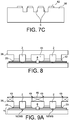
- the element thus obtained is represented on the figure 7B and comprises a plurality of covers 6.
- the cover substrate 38 is prepared for sealing on the NEMS / MEMS structure by means of a dry film.
- the dry film 42 is then fixed on the front face 38.2 of the cover substrate 38, this fixing is advantageously obtained by rolling. This rolling makes it possible to work despite the strong topology due to the existence of the fluid channels on this side of the substrate.
- cords along the cavities etched in the cover It may be a wide cord as shown in the figure 7C , or preferably several narrow cords parallel to each other as shown in the Figures 2A to 2C . In the latter case, for example the cords and the spaces between the cords can be from a few ⁇ m to a few tens of micrometers.
- the beads have a regular structure and a close sealing surface over the entire structure to be sealed so as to ensure a uniform crushing of the dry film with a reasonable pressure during the sealing step.
- the cover substrate 38 is then ready to be sealed on the substrate of the NEMS / MEMS 4 structure.
- the sealing is carried out on sealing equipment which makes it possible to control the temperature and the pressure applied between the cover and the substrate to be sealed.
- the substrate 4 and the cover substrate 38 are aligned by means of the marks made previously on the substrates.
- the pressure applied is of the order of a few kN to a few tens of kN, and for example the temperature is between 100 ° C. and 200 ° C.
- the substrate 4 and the cover substrate 38 are then assembled.
- the fluid channels are then sealed at the lateral edges of the channels.
- the element thus obtained and represented on the figure 8 includes a plurality of fluid channel devices.
- an assembly such as that of the figure 8 is made from circular substrates used in microelectronics.
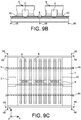
- the separation process firstly comprises a step intended to release the electrical contact pads.
- the contact pads of a device located on one side of the channel 6 are adjacent to those of the neighboring device located on one side of the channel of the neighboring device.
- the step of disengaging the studs is therefore intended to lead into the cavities 44 receiving the studs.
- This step is designated STR for Saw To Reveal in English.
- This step includes cutting the substrate of the cover locally in line with the contact pads so as to open into the cavities 44.
- the cutting lines 45 are symbolized by the broken lines, the cuts delimiting cut portions 46 which are removed.
- This cutting is carried out in the XZ planes, so the sawing residues do not penetrate into the channels.
- a step of precutting of each cover and of the substrate 4 is carried out in planes YZ in a direction perpendicular to the direction X of the fluid channels only so as to longitudinally separate the devices with fluid channels.
- cutting or precut lines are also produced in the substrate 4 in XZ planes parallel to the direction X of the fluid channels so as to transversely separate the devices with fluid channels.
- the fluid channel devices are separated using the precut patterns 48 and 49, for example cleavage, laser cutting.
- sawing is avoided with regard to the production of patterns 48 which would risk polluting the interior of the fluid channels.
- This separation technique is particularly advantageous since it makes it possible to reveal the electrical contact pads while eliminating, at the end of the manufacturing process, any functionalization layer present on the surface of these pads. In addition, it makes it possible to separate the chips from each other while preserving the integrity of the fluid channel.
- the substrate may not include a cavity 44 in the case where the substrate 38 is etched to the contact pads.
- cavities 44 are provided as on the figure 8 , the etching being stopped as soon as one emerges in the cavities, which makes it possible to reveal the contacts. Polishing of the cover substrate may have a bond until it leads to cavities previously formed above the contact pads, technique designated "grinding to reveal" in English. In this case, it is necessary to have cavities of type 44 deeper than the cavities of the fluid channels in order to open into the cavities 44 without opening into the fluid channels in order to preserve their integrity.
- the invention it is possible to produce a fluid channel device comprising one or more mechanical structures suspended in the channel and one or more lateral electrical connections with a guaranteed seal, thus avoiding the formation of TSV in the substrate and also d '' avoid the presence in the fluid channel of structures ensuring electrical contact between the mechanical structure located inside the channel and the outside of this channel, of the metal pillar type extending TSVs made in the cover or of the column type in Si or glass with an engraved cavity inside allowing wire-bonding on a stud of the mechanical structure isolated from the cavity, as is conventionally done with metallic or polymer sealing approaches.
- the invention makes it possible to easily produce networks of mechanical structures by allowing dense and complex electrical interconnection as close as possible to mechanical structures with possibly several levels of metal.
- the invention can also make it possible to encapsulate all the structures and layers present in the channel except the sensitive structures. Finally, it allows the implementation of functionalization during the process on suspended mechanical structures.
Landscapes
- Engineering & Computer Science (AREA)
- Chemical & Material Sciences (AREA)
- Manufacturing & Machinery (AREA)
- Analytical Chemistry (AREA)
- Microelectronics & Electronic Packaging (AREA)
- General Physics & Mathematics (AREA)
- Pathology (AREA)
- Health & Medical Sciences (AREA)
- Biochemistry (AREA)
- General Health & Medical Sciences (AREA)
- Physics & Mathematics (AREA)
- Immunology (AREA)
- Life Sciences & Earth Sciences (AREA)
- Dispersion Chemistry (AREA)
- Nanotechnology (AREA)
- General Chemical & Material Sciences (AREA)
- Oil, Petroleum & Natural Gas (AREA)
- Chemical Kinetics & Catalysis (AREA)
- Micromachines (AREA)
- Physical Or Chemical Processes And Apparatus (AREA)
Claims (19)
- Vorrichtung mit einem Substrat, das mindestens eine mikroelektronische und/oder nanoelektronische Struktur (NEMS) mit mindestens einem abgehängten Abschnitt und einen zwischen dem Substrat und einer Abdeckung (6) definierten Fluidkanal (2) aufweist, wobei der Fluidkanal (2) zwei Seitenwände (6.1) und eine obere Wand (6.2), die die beiden von der Abdeckung gebildeten Seitenwände (6.1) verbindet, und eine untere Wand, die von dem Substrat gebildet wird, sowie mindestens zwei Öffnungen zum Sicherstellen einer Strömung in dem Kanal aufweist, wobei sich die mikroelektronische und/oder nanoelektronische Struktur innerhalb des Fluidkanals befindet, wobei mindestens eine elektrische Verbindungsleitung (8) zwischen der mikroelektronischen und/oder nanoelektronischen Struktur und dem Außenbereich des Fluidkanals (2) verläuft, wobei die Verbindungsleitung (8) auf dem Substrat (4) ausgebildet ist und unter einer der Seitenwände (6.1) verläuft, wobei die Vorrichtung ferner eine Zwischenschicht (20) umfasst, die eine Fläche in Kontakt mit den Basisflächen der Seitenwände (6.1) aufweist, wobei die Fläche der Zwischenschicht die Fähigkeit zur Versiegelung mit den Basisflächen aufweist, wobei die Verbindungsleitung (8) mit der Zwischenschicht (20) mindestens in Höhe der Basisfläche der Seitenwand (6.1) bedeckt ist, wobei die Seitenwände (6.1) durch Ansiegeln an der Zwischenschicht (20) in abgedichteter Weise fest mit dem Substrat (4) verbunden sind.
- Vorrichtung nach Anspruch 1,
enthaltend eine Funktionalisierungsschicht (24, 224), die mindestens einen Teil des abgehängten Abschnitts der mikroelektronischen und/oder nanoelektronischen Struktur einkapselt, wobei die Funktionalisierungsschicht (24, 224) vorteilhafterweise ein oder mehrere Materialien enthält, die aus organischen oder anorganischen Materialien, Polymeren, Oxiden, Halbleitern ausgewählt sind. - Vorrichtung nach Anspruch 1 oder 2,
enthaltend mindestens ein Paar von Verbindungsleitungen (8), die sich seitlich auf beiden Seiten der mikroelektronischen und/oder nanoelektronischen Struktur erstrecken und jeweils unter einer Seitenwand verlaufen (6.1). - Vorrichtung nach Anspruch 1, 2 oder 3,
wobei die Zwischenschicht (20) in dem Fluidkanal (2) die gesamte mikroelektronische und/oder nanoelektronische Struktur mit Ausnahme ihres abgehängten Abschnitts bedeckt. - Vorrichtung nach einem der Ansprüche 1 bis 4,
enthaltend Verbindungsleitungen (8) und Kontaktstücke (9), wobei sich die Kontaktstücke (9) außerhalb des Fluidkanals (2) befinden und die Verbindungsleitungen (8) zwischen der mikroelektronischen und/oder nanoelektronischen Struktur und den Kontaktstücken (9) verlaufen. - Vorrichtung nach einem der Ansprüche 1 bis 5,
wobei die Verbindungsleitungen (8) zumindest innerhalb des Fluidkanals mehrere Metallisierungsebenen aufweisen. - Vorrichtung nach einem der Ansprüche 1 bis 6,
enthaltend einen trockenen Versiegelungsfilm (22), der zwischen der Zwischenschicht (20) und den Basisflächen der Seitenwände (6.1) der Abdeckung angeordnet ist, wobei der trockene Versiegelungsfilm (22) an den Grenzflächen zwischen der Zwischenschicht und den Basisflächen der Seitenwände vorteilhaft in mehrere Stränge strukturiert ist. - Vorrichtung nach einem der Ansprüche 1 bis 7,
enthaltend zumindest eine Materialschicht, die zwischen der Zwischenschicht (20) und den Basisflächen der Seitenwände (6.1) angeordnet ist und eine eutektische Versiegelung, eine Versiegelung durch Thermokompression oder durch Siebdruck, eine molekulare Versiegelung oder eine Glassinterversiegelung bildet. - Vorrichtung nach einem der Ansprüche 1 bis 8,
wobei die Zwischenschicht (20) eine erste Schicht (35) aus elektrisch isolierendem Material in Kontakt mit der Verbindungsleitung (8) und eine zweite Schicht (36), die auf die erste Schicht aufgebracht ist, enthält, wobei die zweite Schicht (36) aus einem Material besteht, das so beschaffen ist, dass es geringfügig oder nicht empfindlich gegenüber einem Schritt des Freisetzens der mikroelektronischen und/oder nanoelektronischen Struktur ist, wobei die zweite Schicht (36) vorteilhaft aus Si, Siliziumnitrid, Metall oder Hafniumoxid besteht. - Vorrichtung nach einem der Ansprüche 1 bis 9,
wobei der Kanal eine Gaschromatographie-Mikrosäule bildet. - Verfahren zum Herstellen zumindest einer Vorrichtung nach einem der Ansprüche 1 bis 10, umfassend die Schritte:a) Herstellen der mikroelektronischen und/oder nanoelektronischen Struktur auf einem Substrat und Herstellen der zumindest einen Verbindungsleitung,b) Ausbilden der Zwischenschicht derart, dass sie eine im Wesentlichen ebene Freifläche aufweist, die eine Öffnung unterhalb des zumindest einen abgehängten Abschnitts aufweist,c) Herstellen eines Abdeckungssubstrats, das einen Fluidkanal aufweist,d) Ansiegeln des Abdeckungssubstrats an die Zwischenschicht, derart, dass der Fluidkanal der mikroelektronischen und/oder nanoelektronischen Struktur gegenüberliegend angeordnet ist.
- Herstellungsverfahren nach Anspruch 11,
umfassend einen Schritt des Herstellens einer Funktionalisierungsschicht innerhalb des Fluidkanals an der mikroelektronischen und/oder nanoelektronischen Struktur und/oder an den Wänden der Abdeckung und/oder an der Zwischenschicht, wobei dieser Schritt vor dem Versiegeln erfolgt. - Herstellungsverfahren nach Anspruch 11 oder 12,
umfassend nach Schritt b) einen Schritt des Freisetzens der mikroelektronischen und/oder nanoelektronischen Struktur. - Herstellungsverfahren nach einem der Ansprüche 11 bis 13,
wobei bei dem Schritt der Versiegelung ein Trockenfilm verwendet wird, wobei das Herstellungsverfahren die folgenden Unterschritte umfasst:- Auflaminieren des Trockenfilms auf die Basisflächen der Wände der Abdeckung,- Strukturieren des Trockenfilms,- Zusammenführen der Abdeckung und des Substrats, welches die mikroelektronischen und/oder nanoelektronischen Strukturen aufweist,- Aufbringen von Druck, um den Trockenfilm zusammenzudrücken, und/oderwobei die Versiegelung eine eutektische Versiegelung oder eine Versiegelung durch Thermokompression oder eine molekulare Versiegelung oder eine Versiegelung durch Siebdruck ist. - Herstellungsverfahren nach einem der Ansprüche 11 bis 14,
wobei das Ausbilden der Zwischenschicht durch Aufbringen einer ersten Schicht aus elektrisch isolierendem Material und durch Aufbringen einer zweiten Schicht auf die erste Schicht erfolgt. - Herstellungsverfahren nach einem der Ansprüche 11 bis 15,
wobei mehrere Vorrichtungen gleichzeitig hergestellt werden, wobei das Substrat mehrere mikroelektronische und/oder nanoelektronische Strukturen enthält und wobei das Abdeckungssubstrat mehrere Abdeckungen aufweist, wobei die Abdeckungen gleichzeitig an das Substrat, das die mikroelektronischen und/oder nanoelektronischen Strukturen enthält, angesiegelt werden, so dass gegebenenfalls ein Fluidkanal einer Vorrichtung mit dem Fluidkanal anderer Vorrichtungen kommunizieren kann. - Herstellungsverfahren nach Anspruch 16,
umfassend die folgenden Schritte:- Herstellen von Vorzuschnitten in einer Richtung senkrecht zu den Fluidkanälen im Abdeckungssubstrat und in dem Substrat, das die mikroelektronischen und/oder nanoelektronischen Strukturen trägt, und/oder- Herstellen von Zuschnitten oder Vorzuschnitten in einer Richtung parallel zu den Fluidkanälen in dem Substrat, das die mikroelektronischen und/oder nanoelektronischen Strukturen trägt,- Trennen der Vorrichtungen, wobei dieses Trennen vorteilhaft durch Spaltung erfolgt. - Herstellungsverfahren nach Anspruch 16 oder 17,
wobei das Abdeckungssubstrat Hohlräume aufweist, die zuvor zwischen den Kanälen gebildet werden und in denen sich die Kontaktstücke nach dem Versiegeln befinden, wobei das Verfahren ferner einen Schritt des Zuschneidens des Abdeckungssubstrats zum Öffnen der Hohlräume umfasst. - Herstellungsverfahren nach Anspruch 18,
wobei bei Ausbilden einer Funktionalisierungsschicht an der mikroelektronischen und/oder nanoelektronischen Struktur und an den Kontaktstücken vor dem Versiegeln das Verfahren den Schritt des Entfernens der Funktionalisierungsschicht an den Kontaktstücken durch Ätzen nach dem Versiegeln und Öffnen der Hohlräume in der Abdeckung umfasst, wobei die Abdeckungen Masken für das Ätzen für die mikroelektronischen und/oder nanoelektronischen Strukturen bilden.
Applications Claiming Priority (1)
| Application Number | Priority Date | Filing Date | Title |
|---|---|---|---|
| FR1357199A FR3008690B1 (fr) | 2013-07-22 | 2013-07-22 | Dispositif comportant un canal fluidique muni d'au moins un systeme micro ou nanoelectronique et procede de realisation d'un tel dispositif |
Publications (3)
| Publication Number | Publication Date |
|---|---|
| EP2829511A2 EP2829511A2 (de) | 2015-01-28 |
| EP2829511A3 EP2829511A3 (de) | 2015-04-08 |
| EP2829511B1 true EP2829511B1 (de) | 2020-06-10 |
Family
ID=49322618
Family Applications (1)
| Application Number | Title | Priority Date | Filing Date |
|---|---|---|---|
| EP14177849.8A Active EP2829511B1 (de) | 2013-07-22 | 2014-07-21 | Vorrichtung, die einen mit mindestens einem mikro- oder nanoelektronischen System ausgestatteten Fluidkanal umfasst, und Herstellungsverfahren einer solchen Vorrichtung |
Country Status (4)
| Country | Link |
|---|---|
| US (1) | US9234879B2 (de) |
| EP (1) | EP2829511B1 (de) |
| CN (1) | CN104326437B (de) |
| FR (1) | FR3008690B1 (de) |
Families Citing this family (8)
| Publication number | Priority date | Publication date | Assignee | Title |
|---|---|---|---|---|
| WO2011154363A2 (en) * | 2010-06-07 | 2011-12-15 | Commissariat à l'énergie atomique et aux énergies alternatives | Analysis device including a mems and/or nems network |
| KR101995293B1 (ko) | 2011-02-21 | 2019-07-02 | 삼성전자 주식회사 | 반송파 집적 기술을 사용하는 시분할 무선통신시스템에서 부차반송파의 활성화 또는 비활성화 방법 및 장치 |
| CN107555398A (zh) * | 2017-07-17 | 2018-01-09 | 西北工业大学 | 一种提高蓝宝石基f‑p腔底部表面质量的mems工艺新方法 |
| US20210319955A1 (en) * | 2018-05-21 | 2021-10-14 | 3M Innovative Properties Company | Ultrathin and flexible devices including circuit dies |
| FR3089630B1 (fr) | 2018-12-07 | 2024-02-02 | Commissariat Energie Atomique | Capteur de flux thermique a nanofilaments chauffants |
| FR3089631B1 (fr) | 2018-12-11 | 2024-02-02 | Commissariat Energie Atomique | Capteur de flux thermique à fil chauffant |
| CN110155934A (zh) | 2019-04-22 | 2019-08-23 | 武汉衍熙微器件有限公司 | 一种mems器件及其制作方法 |
| CN113443602B (zh) * | 2021-06-02 | 2023-12-08 | 中国科学院地质与地球物理研究所 | 微机电系统芯片晶圆级封装结构及其制造工艺 |
Citations (1)
| Publication number | Priority date | Publication date | Assignee | Title |
|---|---|---|---|---|
| FR2957535A1 (fr) * | 2010-03-18 | 2011-09-23 | Bosch Gmbh Robert | Systeme microfluidique pour l'analyse et le diagnostic ainsi que son procede de fabrication |
Family Cites Families (39)
| Publication number | Priority date | Publication date | Assignee | Title |
|---|---|---|---|---|
| US20020022261A1 (en) * | 1995-06-29 | 2002-02-21 | Anderson Rolfe C. | Miniaturized genetic analysis systems and methods |
| US6076409A (en) * | 1997-12-22 | 2000-06-20 | Rosemount Aerospace, Inc. | Media compatible packages for pressure sensing devices |
| US6255728B1 (en) * | 1999-01-15 | 2001-07-03 | Maxim Integrated Products, Inc. | Rigid encapsulation package for semiconductor devices |
| DE19961578A1 (de) * | 1999-12-21 | 2001-06-28 | Bosch Gmbh Robert | Sensor mit zumindest einer mikromechanischen Struktur und Verfahren zur Herstellung |
| TW560018B (en) * | 2001-10-30 | 2003-11-01 | Asia Pacific Microsystems Inc | A wafer level packaged structure and method for manufacturing the same |
| US20070286773A1 (en) * | 2002-05-16 | 2007-12-13 | Micronit Microfluidics B.V. | Microfluidic Device |
| ATE407096T1 (de) * | 2002-05-16 | 2008-09-15 | Micronit Microfluidics Bv | Verfahren zur herstellung eines mikrofluidischen bauteiles |
| US7098117B2 (en) * | 2002-10-18 | 2006-08-29 | The Regents Of The University Of Michigan | Method of fabricating a package with substantially vertical feedthroughs for micromachined or MEMS devices |
| US6936491B2 (en) * | 2003-06-04 | 2005-08-30 | Robert Bosch Gmbh | Method of fabricating microelectromechanical systems and devices having trench isolated contacts |
| US7381583B1 (en) * | 2004-05-24 | 2008-06-03 | The United States Of America As Represented By The Secretary Of The Air Force | MEMS RF switch integrated process |
| US20060171654A1 (en) * | 2004-06-15 | 2006-08-03 | Hawkins Aaron R | Integrated planar microfluidic bioanalytical systems |
| WO2006078968A2 (en) * | 2005-01-20 | 2006-07-27 | Brigham Young University | Integrated planar microfluidic bioanalytical systems |
| EP1843971B1 (de) * | 2005-02-04 | 2016-04-13 | Imec | Verfahren zur verkapselung eines bauelements in einer mikrokavität |
| US7449355B2 (en) * | 2005-04-27 | 2008-11-11 | Robert Bosch Gmbh | Anti-stiction technique for electromechanical systems and electromechanical device employing same |
| US8062497B2 (en) * | 2006-03-28 | 2011-11-22 | Imec | Method for forming a hermetically sealed cavity |
| US7671515B2 (en) * | 2006-11-07 | 2010-03-02 | Robert Bosch, Gmbh | Microelectromechanical devices and fabrication methods |
| US7544531B1 (en) * | 2007-03-13 | 2009-06-09 | Sitime Inc. | Ground strap for suppressing stiction during MEMS fabrication |
| DE102008025599B4 (de) * | 2007-05-14 | 2013-02-21 | Fraunhofer-Gesellschaft zur Förderung der angewandten Forschung e.V. | Gehäuste aktive Mikrostrukturen mit Direktkontaktierung zu einem Substrat |
| US8049326B2 (en) * | 2007-06-07 | 2011-11-01 | The Regents Of The University Of Michigan | Environment-resistant module, micropackage and methods of manufacturing same |
| DE102007060632A1 (de) * | 2007-12-17 | 2009-06-18 | Robert Bosch Gmbh | Verfahren zum Herstellen eines Kappenwafers für einen Sensor |
| CN102209683B (zh) * | 2008-11-10 | 2015-08-05 | Nxp股份有限公司 | 具有侧壁泄露保护的mems器件封装 |
| US8101458B2 (en) * | 2009-07-02 | 2012-01-24 | Advanced Microfab, LLC | Method of forming monolithic CMOS-MEMS hybrid integrated, packaged structures |
| US7989248B2 (en) * | 2009-07-02 | 2011-08-02 | Advanced Microfab, LLC | Method of forming monolithic CMOS-MEMS hybrid integrated, packaged structures |
| FR2948114B1 (fr) | 2009-07-17 | 2012-03-30 | Commissariat Energie Atomique | Nems comportant des moyens de transduction a base d'alliage d'aluminium |
| EP2363373A1 (de) * | 2010-03-02 | 2011-09-07 | SensoNor Technologies AS | Procédé de collage pour systèmes micro et nano sensibles |
| WO2011154363A2 (en) | 2010-06-07 | 2011-12-15 | Commissariat à l'énergie atomique et aux énergies alternatives | Analysis device including a mems and/or nems network |
| US8685778B2 (en) * | 2010-06-25 | 2014-04-01 | International Business Machines Corporation | Planar cavity MEMS and related structures, methods of manufacture and design structures |
| US8507358B2 (en) * | 2010-08-27 | 2013-08-13 | Taiwan Semiconductor Manufacturing Company, Ltd. | Composite wafer semiconductor |
| FR2973944B1 (fr) | 2011-04-06 | 2014-01-10 | Commissariat Energie Atomique | Emetteur pour systeme thermophotovoltaique et systeme thermophotovoltaique comportant au moins un tel emetteur |
| US8671766B2 (en) * | 2011-05-19 | 2014-03-18 | Infineon Technologies Ag | Integrated pressure sensor seal |
| FR2977121B1 (fr) | 2011-06-22 | 2014-04-25 | Commissariat Energie Atomique | Systeme de gestion thermique a materiau a volume variable |
| FR2977885A1 (fr) * | 2011-07-12 | 2013-01-18 | Commissariat Energie Atomique | Procede de realisation d'une structure a electrode enterree par report direct et structure ainsi obtenue |
| FR2981059A1 (fr) * | 2011-10-11 | 2013-04-12 | Commissariat Energie Atomique | Procede d'encapsulation de micro-dispositif par report de capot et depot de getter a travers le capot |
| FR2986908B1 (fr) | 2012-02-14 | 2014-03-28 | Commissariat Energie Atomique | Dispositif de recuperation et de conversion d'energie thermique en energie electrique |
| DE102012210480B4 (de) * | 2012-06-21 | 2024-05-08 | Robert Bosch Gmbh | Verfahren zum Herstellen eines Bauelements mit einer elektrischen Durchkontaktierung |
| US9040355B2 (en) * | 2012-07-11 | 2015-05-26 | Freescale Semiconductor, Inc. | Sensor package and method of forming same |
| FR2999335B1 (fr) | 2012-12-06 | 2016-03-11 | Commissariat Energie Atomique | Procede ameliore de realisation d'un composant a structure suspendue et d'un transistor co-integres sur un meme substrat. |
| US8946831B2 (en) * | 2013-03-12 | 2015-02-03 | Invensense, Inc. | Low frequency response microphone diaphragm structures and methods for producing the same |
| FR3008691B1 (fr) * | 2013-07-22 | 2016-12-23 | Commissariat Energie Atomique | Dispositif comportant un canal fluidique muni d'au moins un systeme micro ou nanoelectronique et procede de realisation d'un tel dispositif |
-
2013
- 2013-07-22 FR FR1357199A patent/FR3008690B1/fr not_active Expired - Fee Related
-
2014
- 2014-07-18 US US14/335,175 patent/US9234879B2/en active Active
- 2014-07-21 CN CN201410347582.0A patent/CN104326437B/zh active Active
- 2014-07-21 EP EP14177849.8A patent/EP2829511B1/de active Active
Patent Citations (1)
| Publication number | Priority date | Publication date | Assignee | Title |
|---|---|---|---|---|
| FR2957535A1 (fr) * | 2010-03-18 | 2011-09-23 | Bosch Gmbh Robert | Systeme microfluidique pour l'analyse et le diagnostic ainsi que son procede de fabrication |
Also Published As
| Publication number | Publication date |
|---|---|
| FR3008690B1 (fr) | 2016-12-23 |
| US20150316517A1 (en) | 2015-11-05 |
| FR3008690A1 (fr) | 2015-01-23 |
| CN104326437A (zh) | 2015-02-04 |
| EP2829511A2 (de) | 2015-01-28 |
| US9234879B2 (en) | 2016-01-12 |
| CN104326437B (zh) | 2017-12-22 |
| EP2829511A3 (de) | 2015-04-08 |
Similar Documents
| Publication | Publication Date | Title |
|---|---|---|
| EP2829511B1 (de) | Vorrichtung, die einen mit mindestens einem mikro- oder nanoelektronischen System ausgestatteten Fluidkanal umfasst, und Herstellungsverfahren einer solchen Vorrichtung | |
| EP3702323B1 (de) | Vorrichtung, die einen mit mindestens einem mikro- oder nanoelektronischen system ausgestatteten fluidkanal umfasst, und herstellungsverfahren einer solchen vorrichtung | |
| EP2863420B1 (de) | Verbessertes Verfahren zum Zusammenbau durch direktes Bonden von zwei Elementen, wobei jedes Element Metallanteile und Anteile aus dielektrischem Material umfasst | |
| EP2546189B1 (de) | Verfahren zur Herstellung einer Struktur mit einer vergrabenen Elektrode durch direkte Übertragung | |
| EP2138451B1 (de) | Verfahren zur Herstellung eines elektromechanischen MEMS-Bauteils in einem einkristallinen Material | |
| EP2952471B1 (de) | Verkapselungsstruktur mit mehreren hohlräumen versehen mit zugangskanälen unterschiedlicher höhe | |
| US20120256308A1 (en) | Method for Sealing a Micro-Cavity | |
| EP2546188B1 (de) | Verfahren zur Herstellung einer Struktur mit einer aufgehängten Membran und einer vergrabenen Elektrode | |
| FR2924421A1 (fr) | Dispositif a circuit integre et n/mems encapsule et procede de realisation. | |
| EP2897162B1 (de) | Einkapselungsstruktur, die teilweise mit Gettermaterial gefüllte Rinnen umfasst | |
| FR2992467A1 (fr) | Procede de realisation d'un composant a contact electrique traversant et composant obtenu | |
| EP2840589B1 (de) | Verbessertes Verfahren zur Trennung zwischen einer aktiven Zone eines Substrats und dessen Rückseite oder eines Teilbereichs seiner Rückseite | |
| EP2581339A2 (de) | Einkapselungsstruktur einer elektronischen Vorrichtung und Herstellungsverfahren einer solchen Struktur | |
| EP3159302B1 (de) | Einkapselungsverfahren eines mikroelektronischen bauteils | |
| EP2661413B1 (de) | Verfahren zum einkapseln einer mikrokomponente | |
| EP3035378B1 (de) | Umwandlungsverfahren einer elektronischen vorrichtung verwendbar in einem verfahren des temporären bondens eines wafers auf ein trägersubstrat und elektronische vorrichtung hergestellt durch das verfahren | |
| EP3165502B1 (de) | Mikroelektronische vorrichtung | |
| FR3074358A1 (fr) | Procede de realisation d'une cavite etanche a couche mince | |
| EP2571045A2 (de) | Flip-Chip-Hybridisierungsverfahren für die Bildung von hermetisch abgeschlossenen Hohlräumen, und durch dieses Verfahren erzielte Systeme | |
| FR3076066A1 (fr) | Procede d'exposition d'une region sur une face d'un dispositif electronique |
Legal Events
| Date | Code | Title | Description |
|---|---|---|---|
| 17P | Request for examination filed |
Effective date: 20140721 |
|
| AK | Designated contracting states |
Kind code of ref document: A2 Designated state(s): AL AT BE BG CH CY CZ DE DK EE ES FI FR GB GR HR HU IE IS IT LI LT LU LV MC MK MT NL NO PL PT RO RS SE SI SK SM TR |
|
| AX | Request for extension of the european patent |
Extension state: BA ME |
|
| PUAI | Public reference made under article 153(3) epc to a published international application that has entered the european phase |
Free format text: ORIGINAL CODE: 0009012 |
|
| PUAL | Search report despatched |
Free format text: ORIGINAL CODE: 0009013 |
|
| AK | Designated contracting states |
Kind code of ref document: A3 Designated state(s): AL AT BE BG CH CY CZ DE DK EE ES FI FR GB GR HR HU IE IS IT LI LT LU LV MC MK MT NL NO PL PT RO RS SE SI SK SM TR |
|
| AX | Request for extension of the european patent |
Extension state: BA ME |
|
| RIC1 | Information provided on ipc code assigned before grant |
Ipc: B81C 1/00 20060101AFI20150305BHEP |
|
| R17P | Request for examination filed (corrected) |
Effective date: 20151007 |
|
| RBV | Designated contracting states (corrected) |
Designated state(s): AL AT BE BG CH CY CZ DE DK EE ES FI FR GB GR HR HU IE IS IT LI LT LU LV MC MK MT NL NO PL PT RO RS SE SI SK SM TR |
|
| STAA | Information on the status of an ep patent application or granted ep patent |
Free format text: STATUS: EXAMINATION IS IN PROGRESS |
|
| 17Q | First examination report despatched |
Effective date: 20181116 |
|
| GRAP | Despatch of communication of intention to grant a patent |
Free format text: ORIGINAL CODE: EPIDOSNIGR1 |
|
| STAA | Information on the status of an ep patent application or granted ep patent |
Free format text: STATUS: GRANT OF PATENT IS INTENDED |
|
| INTG | Intention to grant announced |
Effective date: 20200107 |
|
| GRAS | Grant fee paid |
Free format text: ORIGINAL CODE: EPIDOSNIGR3 |
|
| GRAA | (expected) grant |
Free format text: ORIGINAL CODE: 0009210 |
|
| STAA | Information on the status of an ep patent application or granted ep patent |
Free format text: STATUS: THE PATENT HAS BEEN GRANTED |
|
| AK | Designated contracting states |
Kind code of ref document: B1 Designated state(s): AL AT BE BG CH CY CZ DE DK EE ES FI FR GB GR HR HU IE IS IT LI LT LU LV MC MK MT NL NO PL PT RO RS SE SI SK SM TR |
|
| REG | Reference to a national code |
Ref country code: GB Ref legal event code: FG4D Free format text: NOT ENGLISH |
|
| REG | Reference to a national code |
Ref country code: CH Ref legal event code: EP Ref country code: AT Ref legal event code: REF Ref document number: 1279033 Country of ref document: AT Kind code of ref document: T Effective date: 20200615 |
|
| REG | Reference to a national code |
Ref country code: DE Ref legal event code: R096 Ref document number: 602014066431 Country of ref document: DE |
|
| REG | Reference to a national code |
Ref country code: IE Ref legal event code: FG4D Free format text: LANGUAGE OF EP DOCUMENT: FRENCH |
|
| REG | Reference to a national code |
Ref country code: LT Ref legal event code: MG4D |
|
| PG25 | Lapsed in a contracting state [announced via postgrant information from national office to epo] |
Ref country code: NO Free format text: LAPSE BECAUSE OF FAILURE TO SUBMIT A TRANSLATION OF THE DESCRIPTION OR TO PAY THE FEE WITHIN THE PRESCRIBED TIME-LIMIT Effective date: 20200910 Ref country code: FI Free format text: LAPSE BECAUSE OF FAILURE TO SUBMIT A TRANSLATION OF THE DESCRIPTION OR TO PAY THE FEE WITHIN THE PRESCRIBED TIME-LIMIT Effective date: 20200610 Ref country code: SE Free format text: LAPSE BECAUSE OF FAILURE TO SUBMIT A TRANSLATION OF THE DESCRIPTION OR TO PAY THE FEE WITHIN THE PRESCRIBED TIME-LIMIT Effective date: 20200610 Ref country code: GR Free format text: LAPSE BECAUSE OF FAILURE TO SUBMIT A TRANSLATION OF THE DESCRIPTION OR TO PAY THE FEE WITHIN THE PRESCRIBED TIME-LIMIT Effective date: 20200911 Ref country code: LT Free format text: LAPSE BECAUSE OF FAILURE TO SUBMIT A TRANSLATION OF THE DESCRIPTION OR TO PAY THE FEE WITHIN THE PRESCRIBED TIME-LIMIT Effective date: 20200610 |
|
| REG | Reference to a national code |
Ref country code: NL Ref legal event code: MP Effective date: 20200610 |
|
| PG25 | Lapsed in a contracting state [announced via postgrant information from national office to epo] |
Ref country code: BG Free format text: LAPSE BECAUSE OF FAILURE TO SUBMIT A TRANSLATION OF THE DESCRIPTION OR TO PAY THE FEE WITHIN THE PRESCRIBED TIME-LIMIT Effective date: 20200910 Ref country code: RS Free format text: LAPSE BECAUSE OF FAILURE TO SUBMIT A TRANSLATION OF THE DESCRIPTION OR TO PAY THE FEE WITHIN THE PRESCRIBED TIME-LIMIT Effective date: 20200610 Ref country code: LV Free format text: LAPSE BECAUSE OF FAILURE TO SUBMIT A TRANSLATION OF THE DESCRIPTION OR TO PAY THE FEE WITHIN THE PRESCRIBED TIME-LIMIT Effective date: 20200610 Ref country code: HR Free format text: LAPSE BECAUSE OF FAILURE TO SUBMIT A TRANSLATION OF THE DESCRIPTION OR TO PAY THE FEE WITHIN THE PRESCRIBED TIME-LIMIT Effective date: 20200610 |
|
| REG | Reference to a national code |
Ref country code: AT Ref legal event code: MK05 Ref document number: 1279033 Country of ref document: AT Kind code of ref document: T Effective date: 20200610 |
|
| PG25 | Lapsed in a contracting state [announced via postgrant information from national office to epo] |
Ref country code: AL Free format text: LAPSE BECAUSE OF FAILURE TO SUBMIT A TRANSLATION OF THE DESCRIPTION OR TO PAY THE FEE WITHIN THE PRESCRIBED TIME-LIMIT Effective date: 20200610 Ref country code: NL Free format text: LAPSE BECAUSE OF FAILURE TO SUBMIT A TRANSLATION OF THE DESCRIPTION OR TO PAY THE FEE WITHIN THE PRESCRIBED TIME-LIMIT Effective date: 20200610 |
|
| PG25 | Lapsed in a contracting state [announced via postgrant information from national office to epo] |
Ref country code: AT Free format text: LAPSE BECAUSE OF FAILURE TO SUBMIT A TRANSLATION OF THE DESCRIPTION OR TO PAY THE FEE WITHIN THE PRESCRIBED TIME-LIMIT Effective date: 20200610 Ref country code: IT Free format text: LAPSE BECAUSE OF FAILURE TO SUBMIT A TRANSLATION OF THE DESCRIPTION OR TO PAY THE FEE WITHIN THE PRESCRIBED TIME-LIMIT Effective date: 20200610 Ref country code: EE Free format text: LAPSE BECAUSE OF FAILURE TO SUBMIT A TRANSLATION OF THE DESCRIPTION OR TO PAY THE FEE WITHIN THE PRESCRIBED TIME-LIMIT Effective date: 20200610 Ref country code: SM Free format text: LAPSE BECAUSE OF FAILURE TO SUBMIT A TRANSLATION OF THE DESCRIPTION OR TO PAY THE FEE WITHIN THE PRESCRIBED TIME-LIMIT Effective date: 20200610 Ref country code: RO Free format text: LAPSE BECAUSE OF FAILURE TO SUBMIT A TRANSLATION OF THE DESCRIPTION OR TO PAY THE FEE WITHIN THE PRESCRIBED TIME-LIMIT Effective date: 20200610 Ref country code: CZ Free format text: LAPSE BECAUSE OF FAILURE TO SUBMIT A TRANSLATION OF THE DESCRIPTION OR TO PAY THE FEE WITHIN THE PRESCRIBED TIME-LIMIT Effective date: 20200610 Ref country code: PT Free format text: LAPSE BECAUSE OF FAILURE TO SUBMIT A TRANSLATION OF THE DESCRIPTION OR TO PAY THE FEE WITHIN THE PRESCRIBED TIME-LIMIT Effective date: 20201012 Ref country code: ES Free format text: LAPSE BECAUSE OF FAILURE TO SUBMIT A TRANSLATION OF THE DESCRIPTION OR TO PAY THE FEE WITHIN THE PRESCRIBED TIME-LIMIT Effective date: 20200610 |
|
| PG25 | Lapsed in a contracting state [announced via postgrant information from national office to epo] |
Ref country code: PL Free format text: LAPSE BECAUSE OF FAILURE TO SUBMIT A TRANSLATION OF THE DESCRIPTION OR TO PAY THE FEE WITHIN THE PRESCRIBED TIME-LIMIT Effective date: 20200610 Ref country code: SK Free format text: LAPSE BECAUSE OF FAILURE TO SUBMIT A TRANSLATION OF THE DESCRIPTION OR TO PAY THE FEE WITHIN THE PRESCRIBED TIME-LIMIT Effective date: 20200610 Ref country code: IS Free format text: LAPSE BECAUSE OF FAILURE TO SUBMIT A TRANSLATION OF THE DESCRIPTION OR TO PAY THE FEE WITHIN THE PRESCRIBED TIME-LIMIT Effective date: 20201010 |
|
| REG | Reference to a national code |
Ref country code: CH Ref legal event code: PL |
|
| REG | Reference to a national code |
Ref country code: DE Ref legal event code: R097 Ref document number: 602014066431 Country of ref document: DE |
|
| PG25 | Lapsed in a contracting state [announced via postgrant information from national office to epo] |
Ref country code: MC Free format text: LAPSE BECAUSE OF FAILURE TO SUBMIT A TRANSLATION OF THE DESCRIPTION OR TO PAY THE FEE WITHIN THE PRESCRIBED TIME-LIMIT Effective date: 20200610 |
|
| PLBE | No opposition filed within time limit |
Free format text: ORIGINAL CODE: 0009261 |
|
| STAA | Information on the status of an ep patent application or granted ep patent |
Free format text: STATUS: NO OPPOSITION FILED WITHIN TIME LIMIT |
|
| REG | Reference to a national code |
Ref country code: BE Ref legal event code: MM Effective date: 20200731 |
|
| PG25 | Lapsed in a contracting state [announced via postgrant information from national office to epo] |
Ref country code: LU Free format text: LAPSE BECAUSE OF NON-PAYMENT OF DUE FEES Effective date: 20200721 Ref country code: LI Free format text: LAPSE BECAUSE OF NON-PAYMENT OF DUE FEES Effective date: 20200731 Ref country code: DK Free format text: LAPSE BECAUSE OF FAILURE TO SUBMIT A TRANSLATION OF THE DESCRIPTION OR TO PAY THE FEE WITHIN THE PRESCRIBED TIME-LIMIT Effective date: 20200610 Ref country code: CH Free format text: LAPSE BECAUSE OF NON-PAYMENT OF DUE FEES Effective date: 20200731 |
|
| 26N | No opposition filed |
Effective date: 20210311 |
|
| PG25 | Lapsed in a contracting state [announced via postgrant information from national office to epo] |
Ref country code: BE Free format text: LAPSE BECAUSE OF NON-PAYMENT OF DUE FEES Effective date: 20200731 Ref country code: SI Free format text: LAPSE BECAUSE OF FAILURE TO SUBMIT A TRANSLATION OF THE DESCRIPTION OR TO PAY THE FEE WITHIN THE PRESCRIBED TIME-LIMIT Effective date: 20200610 |
|
| PG25 | Lapsed in a contracting state [announced via postgrant information from national office to epo] |
Ref country code: IE Free format text: LAPSE BECAUSE OF NON-PAYMENT OF DUE FEES Effective date: 20200721 |
|
| PG25 | Lapsed in a contracting state [announced via postgrant information from national office to epo] |
Ref country code: TR Free format text: LAPSE BECAUSE OF FAILURE TO SUBMIT A TRANSLATION OF THE DESCRIPTION OR TO PAY THE FEE WITHIN THE PRESCRIBED TIME-LIMIT Effective date: 20200610 Ref country code: MT Free format text: LAPSE BECAUSE OF FAILURE TO SUBMIT A TRANSLATION OF THE DESCRIPTION OR TO PAY THE FEE WITHIN THE PRESCRIBED TIME-LIMIT Effective date: 20200610 Ref country code: CY Free format text: LAPSE BECAUSE OF FAILURE TO SUBMIT A TRANSLATION OF THE DESCRIPTION OR TO PAY THE FEE WITHIN THE PRESCRIBED TIME-LIMIT Effective date: 20200610 |
|
| PG25 | Lapsed in a contracting state [announced via postgrant information from national office to epo] |
Ref country code: MK Free format text: LAPSE BECAUSE OF FAILURE TO SUBMIT A TRANSLATION OF THE DESCRIPTION OR TO PAY THE FEE WITHIN THE PRESCRIBED TIME-LIMIT Effective date: 20200610 |
|
| PGFP | Annual fee paid to national office [announced via postgrant information from national office to epo] |
Ref country code: DE Payment date: 20250722 Year of fee payment: 12 |
|
| PGFP | Annual fee paid to national office [announced via postgrant information from national office to epo] |
Ref country code: GB Payment date: 20250724 Year of fee payment: 12 |
|
| PGFP | Annual fee paid to national office [announced via postgrant information from national office to epo] |
Ref country code: FR Payment date: 20250722 Year of fee payment: 12 |