EP3702323B1 - Vorrichtung, die einen mit mindestens einem mikro- oder nanoelektronischen system ausgestatteten fluidkanal umfasst, und herstellungsverfahren einer solchen vorrichtung - Google Patents
Vorrichtung, die einen mit mindestens einem mikro- oder nanoelektronischen system ausgestatteten fluidkanal umfasst, und herstellungsverfahren einer solchen vorrichtung Download PDFInfo
- Publication number
- EP3702323B1 EP3702323B1 EP20171331.0A EP20171331A EP3702323B1 EP 3702323 B1 EP3702323 B1 EP 3702323B1 EP 20171331 A EP20171331 A EP 20171331A EP 3702323 B1 EP3702323 B1 EP 3702323B1
- Authority
- EP
- European Patent Office
- Prior art keywords
- substrate
- layer
- nems
- microelectronic
- sealing
- Prior art date
- Legal status (The legal status is an assumption and is not a legal conclusion. Google has not performed a legal analysis and makes no representation as to the accuracy of the status listed.)
- Not-in-force
Links
Images







Classifications
-
- B—PERFORMING OPERATIONS; TRANSPORTING
- B81—MICROSTRUCTURAL TECHNOLOGY
- B81B—MICROSTRUCTURAL DEVICES OR SYSTEMS, e.g. MICROMECHANICAL DEVICES
- B81B7/00—Microstructural systems ; Auxiliary parts of microstructural devices or systems
- B81B7/0032—Packages or encapsulation
- B81B7/0061—Packages or encapsulation suitable for fluid transfer from the MEMS out of the package or vice versa, e.g. transfer of liquid, gas, sound
-
- B—PERFORMING OPERATIONS; TRANSPORTING
- B81—MICROSTRUCTURAL TECHNOLOGY
- B81B—MICROSTRUCTURAL DEVICES OR SYSTEMS, e.g. MICROMECHANICAL DEVICES
- B81B7/00—Microstructural systems ; Auxiliary parts of microstructural devices or systems
- B81B7/0032—Packages or encapsulation
- B81B7/007—Interconnections between the MEMS and external electrical signals
-
- B—PERFORMING OPERATIONS; TRANSPORTING
- B81—MICROSTRUCTURAL TECHNOLOGY
- B81C—PROCESSES OR APPARATUS SPECIALLY ADAPTED FOR THE MANUFACTURE OR TREATMENT OF MICROSTRUCTURAL DEVICES OR SYSTEMS
- B81C1/00—Manufacture or treatment of devices or systems in or on a substrate
- B81C1/00015—Manufacture or treatment of devices or systems in or on a substrate for manufacturing microsystems
- B81C1/00261—Processes for packaging MEMS devices
- B81C1/00269—Bonding of solid lids or wafers to the substrate
-
- B—PERFORMING OPERATIONS; TRANSPORTING
- B81—MICROSTRUCTURAL TECHNOLOGY
- B81C—PROCESSES OR APPARATUS SPECIALLY ADAPTED FOR THE MANUFACTURE OR TREATMENT OF MICROSTRUCTURAL DEVICES OR SYSTEMS
- B81C1/00—Manufacture or treatment of devices or systems in or on a substrate
- B81C1/00015—Manufacture or treatment of devices or systems in or on a substrate for manufacturing microsystems
- B81C1/00261—Processes for packaging MEMS devices
- B81C1/00309—Processes for packaging MEMS devices suitable for fluid transfer from the MEMS out of the package or vice versa, e.g. transfer of liquid, gas, sound
-
- G—PHYSICS
- G01—MEASURING; TESTING
- G01N—INVESTIGATING OR ANALYSING MATERIALS BY DETERMINING THEIR CHEMICAL OR PHYSICAL PROPERTIES
- G01N30/00—Investigating or analysing materials by separation into components using adsorption, absorption or similar phenomena or using ion-exchange, e.g. chromatography or field flow fractionation
- G01N30/02—Column chromatography
- G01N30/60—Construction of the column
- G01N30/6095—Micromachined or nanomachined, e.g. micro- or nanosize
-
- B—PERFORMING OPERATIONS; TRANSPORTING
- B81—MICROSTRUCTURAL TECHNOLOGY
- B81B—MICROSTRUCTURAL DEVICES OR SYSTEMS, e.g. MICROMECHANICAL DEVICES
- B81B2201/00—Specific applications of microelectromechanical systems
- B81B2201/02—Sensors
- B81B2201/0214—Biosensors; Chemical sensors
-
- B—PERFORMING OPERATIONS; TRANSPORTING
- B81—MICROSTRUCTURAL TECHNOLOGY
- B81B—MICROSTRUCTURAL DEVICES OR SYSTEMS, e.g. MICROMECHANICAL DEVICES
- B81B2201/00—Specific applications of microelectromechanical systems
- B81B2201/02—Sensors
- B81B2201/0292—Sensors not provided for in B81B2201/0207 - B81B2201/0285
-
- B—PERFORMING OPERATIONS; TRANSPORTING
- B81—MICROSTRUCTURAL TECHNOLOGY
- B81B—MICROSTRUCTURAL DEVICES OR SYSTEMS, e.g. MICROMECHANICAL DEVICES
- B81B2201/00—Specific applications of microelectromechanical systems
- B81B2201/05—Microfluidics
- B81B2201/058—Microfluidics not provided for in B81B2201/051 - B81B2201/054
-
- B—PERFORMING OPERATIONS; TRANSPORTING
- B81—MICROSTRUCTURAL TECHNOLOGY
- B81B—MICROSTRUCTURAL DEVICES OR SYSTEMS, e.g. MICROMECHANICAL DEVICES
- B81B2207/00—Microstructural systems or auxiliary parts thereof
- B81B2207/07—Interconnects
-
- B—PERFORMING OPERATIONS; TRANSPORTING
- B81—MICROSTRUCTURAL TECHNOLOGY
- B81B—MICROSTRUCTURAL DEVICES OR SYSTEMS, e.g. MICROMECHANICAL DEVICES
- B81B2207/00—Microstructural systems or auxiliary parts thereof
- B81B2207/09—Packages
- B81B2207/091—Arrangements for connecting external electrical signals to mechanical structures inside the package
- B81B2207/094—Feed-through, via
- B81B2207/096—Feed-through, via through the substrate
-
- B—PERFORMING OPERATIONS; TRANSPORTING
- B81—MICROSTRUCTURAL TECHNOLOGY
- B81C—PROCESSES OR APPARATUS SPECIALLY ADAPTED FOR THE MANUFACTURE OR TREATMENT OF MICROSTRUCTURAL DEVICES OR SYSTEMS
- B81C2203/00—Forming microstructural systems
- B81C2203/01—Packaging MEMS
- B81C2203/0118—Bonding a wafer on the substrate, i.e. where the cap consists of another wafer
Definitions
- the present invention relates to a device comprising a fluidic channel provided with at least one micro or nanoelectronic system and to a method for producing such a device.
- microelectronic or nanoelectronic systems include microelectromechanical systems or MEMS (microelectromechanical systems in English) and nanoelectromechanical systems or NEMS (Nanoelectromechanical systems).
- MEMS microelectromechanical systems in English
- NEMS Nanoelectromechanical systems
- MEMS and NEMS are now widely used in many products. New applications are appearing in particular due to the development of NEMS which offer new advantages thanks to the reduction in dimensions. In particular, because of the great mass sensitivity of this type of system, they are of great interest for chemical or biological sensors.
- a NEMS or a MEMS comprises a fixed part and at least one sensitive part possibly suspended, relative to the fixed part.
- the MEMS or NEMS type structure which offers particular physicochemical characteristics, to a surrounding medium, generally gaseous or liquid.
- the MEMS or NEMS sensitive structure is placed in a fluidic channel in which the medium flows and allows the medium to be analyzed to come into contact with the NEMS or MEMS sensitive structure.
- the fluidic channel is produced by attaching a cover to a substrate comprising the sensitive structure (s).
- the cover is sealed on the substrate and has at least two openings to ensure circulation in the channel of the fluid to be analyzed.
- the cover comprises a cavity made in a substrate, from several ⁇ m to several hundreds of ⁇ m in depth for example.
- the document WO2011 / 154363 describes an analysis device, for example a gas chromatography microcolumn comprising MEMS and / or NEMS in the microcolumn, forming sensors.
- the microcolumn is formed of a substrate and a cover.
- the connection of MEMS and / or NEMS is achieved for example by vias made in the substrate and opening at the assembly interface between the cover and the substrate.
- Connection lines connect the vias to sensitive structures. The presence of these vias at the assembly interface makes the assembly complex and, in addition, the electrical connection of the sensitive structures with the exterior is made complex due to the production of the vias and the connection lines.
- the sealing of the cover can use techniques such as polymer sealing, molecular sealing, anodic sealing, eutectic sealing, glass sintering, etc.
- the problem then arises of making the electrical connections between the sensitive structure or structures located inside the fluidic channel and the outside of the fluidic channel since the seal, while allowing these electrical connections, must be sealed.
- One technique consists, after sealing of the cover, in opening large cavities in the thickness of the cover only above the zones of metallized pads to allow direct resumption of contact by wirebonding on these pads, each contact pad being surrounded by a sealing bead, for example of polymer, to isolate this part of the cavity.
- this technique has the drawback of introducing additional patterns for these electrical passages inside the fluidic channel, which is undesirable because they can be the source of disturbance in the circulation of the fluid, of the generation of dead volumes, etc.
- this technique is ill-suited in the case of sensitive structures of the NEMS or MEMS type because these structures require contact pads made of semiconductor material or of small metal in order to reduce the parasitic capacitances and to be able to extract a signal electrically usable with a good signal / noise ratio.
- this technique is not suitable for components formed from NEMS or MEMS in networks, because they must be interconnected with one another with a high density, which implies the implementation of very small size pads, and possibly put implemented several metallic levels.
- TSV Through Silicon Via in English
- TGV Through Glass Via in English
- 3D MEMS high vaccum wafer level packaging S. Nicolas et al. Electronic Components and Technology Conference (ECTC), 2012 IEEE 62nd, Date of Conference: May 29 2012-June 1 2012 , describes such achievements.
- TSV type connections would for example be made in the thickness of the cover and would open into the cavity, the electrical continuity then being ensured by a metal pad / bead inside the cavity.
- the document US 2008/283991 A1 describes a device comprising a fluidic channel provided with a microelectromechanical system.
- the device comprises electrical connections between this microelectromechanical system and the outside of the fluidic channel, the electrical connections being formed by vias made through the substrate on which the microelectromechanical system rests, and this in line with the microelectromechanical system and in contact. electric with this one.
- the document US2012 / 138460 A1 describes a biosensor arranged in a fluidic channel.
- a device comprising a substrate comprising at least one microelectronic and / or nanoelectronic structure comprising at least one sensitive part and a fluidic channel defined between said substrate and a cover, said fluidic channel comprising at least two openings to ensure circulation in said channel, said microelectronic and / or nanoelectronic structure being located inside the fluidic channel, said cover being assembled with the substrate at the level of an assembly interface, said device comprising at least one electrical connection between said microelectronic and / or nanoelectronic structure and the outside of the fluidic channel, said electrical connection being formed by a via made through the substrate directly above said microelectronic and / or nanoelectronic structure and in electrical contact with said microelectronic structure and / or nanoelectronics, the device also comprising a couch e functionalization covering at least part of the sensitive part of the microelectronic and / or nanoelectronic structure.
- the microelectronic and / or nanoelectronic structure comprises a fixed structure including contact pads, at least one sensitive structure and means for actuating and / or transducing at least one characteristic of the sensitive structure, the pads contact being electrically connected to the sensitive part and / or to the fixed part.
- the assembly of the cover and the substrate is simplified.
- the via plumb with the microelectronic and / or nanoelectronic structure it is in direct contact with the corresponding contact pad. No additional conductive track is required between the via and its contact pad.
- the fact of placing the stud in the fluidic channel makes it possible to limit the length conductive track necessary between the pad and the sensitive part, or even the fixed part, and thus to optimize the quality in particular of the electrical transduction signal.
- NEMS / MEMS network it is possible to directly connect each of the NEMS / MEMS structures present in the fluidic channel of individually, thus making it possible, for example, to control and optimize the characteristics of the network.
- the vias or vias do not disturb the flow in the channel since they do not open into the flow of the fluid, they are masked below the microelectronic and / or nanoelectronic structure.
- the invention therefore makes it possible not to resort to making a via through the cover and / or to opening large cavities in the thickness of the cover to allow contact to be resumed.
- the vias are made through the substrate directly below the microelectronic and / or nanoelectronic structure.
- an intermediate layer can be provided between the cover and the substrate to facilitate assembly.
- the intermediate layer may have a surface condition allowing sealing with the base faces of the cover, for example a seal by dry film, a molecular seal, eutectic or by thermocompression.
- the face suitable for sealing may have a certain roughness or a certain relief which nevertheless allows sealing.
- the intermediate layer can be provided in the fluidic channel, the intermediate layer can be such that it encapsulates the materials of the NEMS or MEMS structure, except the sensitive part, which by virtue of their presence in the fluidic channel, could interact with the medium circulating in the channel, ie it isolates the materials of the NEMS or MEMS structure other than the sensitive part of the interior of the fluidic channel.
- the intermediate layer is advantageously only open at the level of the NEMS or MEMS structures intended to interact with the surrounding environment.
- the sensitive structure is functionalized.
- the assembly is carried out by means of a dry film, such an assembly method is particularly suitable in the case of a functionalization of the sensitive structure.
- the via (s) is or are produced after assembly of the cover on the substrate, which makes it possible to thin the substrate and to produce dense vias, the hood serving as a handle.
- the structure according to the invention and its production method allow a collective production of chips provided with a fluidic channel, the chips being separated by sawing between the channels and by precut transverse to the channels.
- the subject of the present invention is therefore a device as recited in claim 1.
- the via may be in electrical contact with the microelectronic and / or nanoelectronic structure via a contact pad located in the fluidic channel.
- the device can very advantageously comprise an intermediate layer located at least partly in the fluidic channel, said intermediate layer covering, in the fluidic channel, at least in part the microelectronic and / or nanoelectronic structure with the exception of its sensitive part or a intermediate layer located only at the assembly interface located between the cover and the substrate.
- the intermediate layer may include an electrically insulating material, such as a silicon oxide, or a silicon nitride.
- the device may include several microelectronic and / or nanoelectronic structures interconnected in said fluidic channel. Microelectronic and / or nanoelectronic structures can interconnect with one another by interconnection lines located in the fluidic channel.
- the intermediate layer electrically insulates the interconnection lines.
- the device comprises a dry sealing film interposed between the substrate and the cover.
- the dry sealing film may have several beads.
- the device comprises at least one layer of material interposed between the substrate and the cover providing an eutectic or metallic seal or by thermo-compression, or by screen printing or a molecular seal or a seal by sintering of glass.
- the intermediate layer can advantageously comprise at least a first planarizing layer and a second layer deposited on the first layer, said second layer being made of a material such that it is little or not sensitive to a step of releasing the microelectronic structure and / or nanoelectronics.
- the first layer has a sufficient thickness to erase the variations in topology and it is advantageously insulating when the intermediate layer is on the contact pads of the microelectronic and / or nanoelectronic structure.
- the channel can advantageously form a gas chromatography microcolumn.
- a subject of the present invention is also a method for producing at least one device according to the invention, as recited in claim 8.
- Step d) takes place after step c).
- the method may comprise, prior to the production of at least one via and after step d), a step of thinning the substrate.
- the method may comprise, prior to the step of filling said hole with an electrically conductive material, a step of depositing on the internal surface of the hole an electrically insulating material.
- making the hole is obtained by deep etching then by fine etching.
- the method may also include a step of forming an intermediate layer on the substrate after step a) in a zone such that it comprises at least one part located in the fluidic channel after step d) or a step of formation of an intermediate layer on the substrate after step a) in an area such that it is located only at the assembly interface after step d).
- the method may include, during step a), the production in the microelectronic and / or nanoelectronic structure of at least one electrical contact pad intended to ensure electrical contact with the via.
- the method can then further comprise, in order to form said contact pad, an additional metallic deposit thereon.
- the method may also include a step of producing an electrical distribution layer on the face of the device into which said via emerges.
- the seal is a eutectic or metallic seal by thermo-compression, or by molecular sealing or by screen printing.
- the substrate then comprises several microelectronic and / or nanoelectronic structures and the cover substrate comprises several covers, the covers being sealed simultaneously on the substrate comprising the microelectronic and / or nanoelectronic structures, so that a fluidic channel of a device may or may not communicate with the fluidic channel of other devices.
- NEMS / MEMS part is understood to mean a mechanical structure comprising a fixed structure and at least one sensitive structure and means for actuating and / or transducing at least one characteristic of the sensitive structure.
- This MEMS / NEMS part can include a network of NEMS and / or MEMS structures, possibly with several metallization levels to achieve the interconnections required.
- a MEMS or a NEMS will be referred to as NEMS.
- the "sensitive part” can be a suspended part or not. In the remainder of the description, these two expressions will be used interchangeably, knowing that in certain electromechanical type applications this sensitive part is mobile.
- NEMS structure is understood to mean a structure comprising one or more NEMS.
- the fluidic channel is rectilinear with axis X, but a channel having a curved shape, even a spiral or any other shape does not go beyond the scope of the present invention.
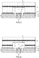
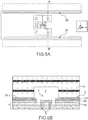
- a top view schematically represented can be seen of a fluidic channel device according to a first exemplary embodiment, the top of the cover being omitted.
- a cross-sectional view can be seen along the plane AA 'of the figure 1 . In this view, the top of the cover 6 is shown.
- the device comprises a fluidic channel 2 which is rectilinear with axis X in the example shown.
- the fluidic channel 2 is delimited by a substrate 4 and a cover 6 transferred to the substrate 4 and assembled at the level of an assembly interface 3.
- the flow in the fluidic channel takes place from a longitudinal end 2.1 to the other 2.2 of the fluidic channel 2.
- the cover 6 is formed from a substrate in which a cavity 5 has been formed.
- the cavity 5 defines with the substrate carrying the NEMS / MEMS structure and the assembly interface 3 the fluidic channel 2 which ensures the circulation and distribution of a gas or liquid mixture.
- the channel is delimited by two side walls 6.1, an upper bottom 6.2 connecting the two side walls 6.1 and a lower bottom formed by the substrate 4.
- the side walls 6.1 have base faces which allow the sealing of the cover on the substrate.
- inlet end and / or the outlet end of the fluidic channel could for example be produced in the upper bottom 6.2 of the channel or in the substrate 4.
- the cover 6 could have a more complex shape, for example it could include a long channel of optimized shape, for example in a spiral, making it possible to produce a chromatography column ensuring the function of separating the compounds from a mixture, the column integrating one or more NEMS / MEMS structures.
- the cover 6 is assembled on the substrate 4 by sealing.
- the substrate comprises a NEMS / MEMS 7 structure located inside the fluidic channel 2.
- the suspended structure of the NEMS is formed by a beam 10 embedded at one of its longitudinal ends, for example two gauges. 12, for example two piezoresistive gauges, are used to detect the displacement of the beam 10.
- the ends of the connection lines 8 connected to the NEMS / MEMS structure are used to detect the displacement of the beam 10.
- the device also comprises electrical connections 8 extending between the NEMS located in the fluidic channel 2 and the exterior of the fluidic channel.
- the electrical connections 8 are formed by vias crossing the substrate 4, also called TSV (Through Silicon Via).
- TSV Through Silicon Via
- the vias cross the substrate 4 in line with the NEMS structure located in the fluidic channel and outside the assembly zone, more particularly in line with the fixed part of the NEMS. In the representation of the figure 2 , the vias are made under the NEMS.
- the vias are produced according to a via last approach, i.e. after the realization of the NEMS structure (s).
- the vias then have a diameter of a few ⁇ m, they are well suited to mechanical structures and they offer relatively high densities since the pitch between these vias can be of the order of around ten ⁇ m.
- the vias can be made from different materials such as Cu, W, etc.
- the vias can be large holes etched and covered with a conductive material ensuring electrical continuity between the two faces of the substrate.
- the vias can be formed by relatively narrow holes completely filled with a more or less conductive material, for example polysilicon.
- a narrow hole has for example a diameter of about a few ⁇ m and a wide hole has for example a diameter of about a few tens of ⁇ m to a few hundred ⁇ m.
- the via (s) can come into contact with the lower face of the layer 16 in which the NEMS (s) are formed.
- the vias or vias can come into contact with the upper face of the layer 16, preferably by means of a metal stud formed on the surface of the layer 16.
- the vias or vias can make contact on a metallic interconnection layer produced in a plane parallel to the plane of the NEMS (s), on the side of the fluidic channel, for example on one of the interconnection levels of the NEMS networks which will be described below or on the side of the substrate in which these connection patterns are made. It could also be envisaged that the vias come into contact on a metallic interconnection layer produced in a plane parallel to the plane of the NEMS (s), but on the side opposite to the fluidic channel to connect to external elements located, for example at the back of MEMS
- the substrate 4 comprises a stack of a sacrificial layer 14 used for the production of the NEMS, of a layer 16 for example of semiconductor in which the fixed part and the suspended part of the NEMS are made.
- the vias do not open into the assembly interface 3, the assembly interface can then be free of a metal layer. It is then possible to make assemblies with very efficient sealing techniques in terms of robustness, reliability and hermeticity.
- the absence of a via opening into the sealing interface or of connection lines between the cover and the substrate makes it possible to have a flat surface.
- techniques such as molecular sealing, eutectic sealing (AuSn, AuSi, etc.), sealing by metal thermo-compression (Au-Au, Al-Ge) can be envisaged.
- Metal thermo-compression seals are particularly advantageous because they make it possible to reduce the sealing temperature below 400 ° C. or even 200 ° C., which is particularly advantageous when a functionalization layer is implemented.
- molecular sealing which can be carried out at low temperature is advantageous for the same reasons of preserving a possible functionalization layer.
- this deposition and this possible structuring are preferably carried out. on the hood.
- an Au layer is preferably deposited on the cover.
- the deposition on the NEMS / MEMS structure is carried out before the release of the structure.
- the material of this layer is then chosen to be compatible with the process for releasing the NEMS / MEMS structure so that it is not etched during this technological step which takes place just before sealing.
- a layer of Au will be used on the cover and on the intermediate layer for an Au-Au seal, in the case of a release of the NEMS with hydrofluoric acid in the vapor phase.
- the sealing interface is formed by the face of the cover and the face of the substrate to be sealed. No addition of material is required.
- the faces intended to come into contact are prepared in a manner known to those skilled in the art, for example by chemical-mechanical polishing (or CMP (chemical-mechanical polishing) in English), of the layer 16 and the underside of the cover 6 .
- the vias are made after sealing the cover on the substrate.
- high temperature seals can be envisaged, all the more so if there are no active structures of the CMOS type on the substrate.
- vias in the fluidic channel makes it possible to produce devices with a greater number and / or a greater density of electrical outputs from the NEMS structures contained in the fluidic channel to the outside of this channel. This therefore results in a possibility of having a greater density of NEMS structures (in networks or not) inside the fluidic channel, which is particularly advantageous in the case of a gas chromatography microcolumn in which NEMS / MEMS structures are distributed throughout the microcolumn.
- this density can be increased by making vias of small diameters, for example a few ⁇ m or a few 10 ⁇ m. of diameter.
- the vias being produced in the substrate they are produced independently of the thickness of the “cover” layer. It is then possible to achieve dense vias and a deep cavity. This advantage is remarkable in particular in the case of an instrumented microcolumn which requires dense vias, requiring a thinning of the thickness of the NEMS substrate to a few 10 ⁇ m and a dimension of the cavities of the microcolumn of at least 100 ⁇ m. In fact, the typical dimensions of the section of the channel are 80 ⁇ 80 ⁇ m or even more for the needs of the application for separating the analytes constituting the gas mixture circulating in the channel.
- the vias are produced after assembly with the cover, which then allows sufficient thinning of the substrate, for example a few tens of ⁇ m, to produce sufficiently dense vias, the cover ensuring mechanical rigidity.
- the invention makes it possible to fabricate a device with complex arrays of NEMS within the fluidic channel and very good control of these arrays, by individual addressing of each NEMS structure via the TSVs.
- the materials at the sealing interface such as silicon, metals, oxides, etc. are generally more neutral compared to the species (gas for example), circulating in the fluidic channel, compared to a layer glue, which risks to degas and may exhibit a disturbing chemical affinity with respect to circulating species.
- This advantage is particularly advantageous in the example of a fluidic channel intended for the production of a gas phase chromatography column.
- the device comprises a functionalization layer 18 covering the layer 16 and the entire NEMS / MEMS structure.
- This functionalization layer 18 is said to be non-localized.
- the term “functionalization layer” is understood to mean a layer present at the surface of the mechanical structure in order to provide it with particular properties.
- the functionalization layer makes it possible to increase the adsorption of gaseous species in an optionally selective manner or, in the case of a biological sensor, the functionalization layer makes it possible to ensure grafting of biological species.
- the functionalization layer 18 is for example formed from one or more organic or inorganic materials, polymers, oxides, carbon compounds, semiconductors or other porous materials.
- the invention very advantageously makes it possible to carry out the step of depositing the functionalization layer on an already released mechanical structure, which makes it possible to almost completely encapsulate the mechanical structure with the functionalization layer when the deposition thereof is sufficiently compliant.
- the functionalization layer then has an increased interaction surface with the surrounding medium, which further increases the value of a functionalization layer.
- the invention allows the implementation of functionalization layers on NEMS released by non-contact liquid and collective techniques, for example by CVD deposition, LPCVD, PECVD, ALD, epitaxy, porosification, etc. and then to continue by the deposition. closing the component by attaching a cover comprising a cavity so as to form the fluidic channel Thus the risks of sticking by deposition of the functionalization layer by liquid phase deposition are avoided.
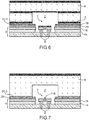
- the functionalization layer 118 is only present on the sensitive part of the NEMS, the functionalization layer is said to be localized.
- the invention makes it possible to carry out the step of depositing the functionalization layer on an already released mechanical structure, which makes it possible to almost completely encapsulate the mechanical structure with the functionalization layer when the deposit thereof is sufficiently compliant.
- the functionalization layer covers the upper face, the lower face and the side faces of the suspended element.
- the functionalization layer then has an increased interaction surface with the surrounding medium, which further increases the value of a functionalization layer.
- the invention allows the implementation of functionalization layers on NEMS released by non-contact and collective techniques, for example by CVD deposition, LPCVD, PECVD, ALD, epitaxy, porosification, etc. and then to continue with the closure of the component by attaching a cover comprising a cavity so as to form the fluidic channel Thus the risks of sticking by deposition of the functionalization layer by liquid phase deposition are avoided.
- the intermediate layer 20 is disposed at the assembly interface only. It is interposed between the semiconductor layer 16 and the cover 6.
- the presence of the intermediate layer 20 at the assembly interface makes assembly easier.
- the intermediate layer may have a surface condition allowing sealing with the base faces of the cover, for example sealing by dry film, molecular sealing, eutectic or by thermocompression.
- the face suitable for sealing may have a certain roughness or a certain relief which nevertheless allows sealing.
- the intermediate layer 20 is present at least at the level of the sealing interface between the NEMS / MEMS structure 7 and the cover and is absent from the sensitive areas of the NEMS / MEMS structure in order to leave the part (s) of the NEMS / structure. MEMS suspended in contact with the medium present in the fluidic channel.
- the material of the intermediate layer 20 is chosen so as to make it possible to obtain a face 20.2 that is sufficiently flat for sealing the cover.
- the surface condition of the face 20.2 obtained directly after the deposition of the intermediate layer may be sufficient, or a step of planarization is carried out for example a mechanical-chemical polishing step after the formation of the intermediate layer.
- the material of the intermediate layer is chosen capable of being etched, for example by anisotropic etching.
- the material of the intermediate layer 20 is chosen so as to have good selectivity for etching with respect to the process for releasing the mechanical structures and not to generate any residue during this step.
- the material of the intermediate layer is also chosen so as to be compatible with the materials used for the final assembly of the device between the substrate carrying the NEMS / MEMS structure and the cover.
- the material of the intermediate layer is chosen to be compatible with that of the functionalization layer, in particular so as to ensure good adhesion of the latter.
- the material of the intermediate layer is a dielectric material, for example a silicon oxide, such as for example SiO 2 or an oxide formed based on silane or an oxide formed based on tetraethylorthosilicate (TEOS), an oxide of LTO (Low Temperature Oxide) type silicon formed by low pressure chemical vapor deposition or LPCVD (Low Pressure Chemical Vapor Deposition) undoped or doped with phosphorus (PSG: phospho-Silicate-Glass) or doped with Boron and Phosphorus (BPSG: Boro-Phospho-Silicate Glass), an oxide deposited by plasma enhanced chemical vapor deposition or PECVD (Plasma Enhanced Chemical Vapor Deposition).
- a silicon oxide such as for example SiO 2 or an oxide formed based on silane or an oxide formed based on tetraethylorthosilicate (TEOS)
- LTO Low Temperature Oxide
- LPCVD Low Pressure Chemical Vapor Deposition
- PSG
- the thickness of the intermediate layer is determined to take into account the consumption of material during the release etching.
- the thickness of the intermediate layer is for example of the order of a few ⁇ m.
- the intermediate layer can comprise two layers.
- a layer of dielectric material forming the planarizing layer is deposited.
- the planarizing layer is for example an oxide formed based on silane SiH 4 , or else an oxide formed based on tetraethylorthosilicate (TEOS).
- TEOS tetraethylorthosilicate
- a protective layer for example in amorphous Si, in silicon nitride, in metal (AISi, AlCu, etc.), in Hafnium oxide (HfO2), is then deposited on the planarizing layer, the latter increasing the resistance to etching with hydrofluoric acid vapor
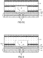
- the intermediate layer 120 is located at the sealing interface and inside the fluidic channel.
- the intermediate layer delimits a channel 21 inside the channel of a width such that it leaves free the sensitive parts of the NEMS structure.
- the intermediate layer leaves free only the sensitive parts of the NEMS structure, the intermediate layer being present upstream and downstream of the NEMS structure.
- the intermediate layer in addition to its presence at the sealing interface, the intermediate layer encapsulates the materials used at the level of the NEMS so as to leave accessible for the fluid circulating in the fluidic channel only the sensitive part of the NEMS or of a network of NEMS.
- This encapsulation has the advantage of isolating the materials involved in the NEMS part which, by virtue of their presence in the fluidic channel 2, could interact with the medium circulating in the channel. This is the case, for example, with metals or dielectrics which are generally used in the fluidic channel if the mechanical structure is formed from a dense network of NEMS.
- a fluidic channel device in which the intermediate layer does not entirely cover the part of the NEMS / MEMS structure not intended to come into contact with the surrounding medium is not outside the scope of the present invention.
- the intermediate layer forms a quasi-planar surface in the environment of the sensitive parts of the NEMS, forming a fourth face of the fluidic channel.
- the intermediate layer 120 is present above the layer 16 in which the NEMS is produced, which is for example made of semiconductor, at the level of the vias which are for example made of metal.
- the presence of the intermediate layer mechanically reinforces the structure in particular vis-à-vis the mechanical stresses which can be generated at the level of the vias, for example due to the differences in thermal expansion coefficients, between the material of the vias and the surrounding material in which these vias are formed. The reliability of the device is then improved.
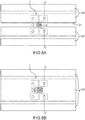
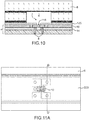
- encapsulation layer 220 which is present only inside the fluidic channel and covers the materials used at the level of the NEMS .
- the encapsulation layer 220 has the same advantages as those of the layer 120 except those relating to the sealing.
- the device of figures 11A and 11B may comprise a functionalization layer located on the sensitive parts of the NEMS structure or not, it would then be located at the assembly interface, on the encapsulation layer 220 and the sensitive parts of the NEMS structure.
- NEMS may or may not be connected to each other.
- An example of an interconnected NEMS device will be described below.
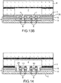
- an intermediate layer 120 is formed between the cover and the substrate and in the channel leaving free only the sensitive parts of the NEMS structures.
- a device comprising a network of interconnected NEMS.
- the interconnections between NEMS are made by conductive connections, preferably metallic 24 formed on the NEMS in the fluidic channel.
- Interconnection lines 24 are then made on several metal levels, two in the example shown, in order to connect the NEMSs forming the NEMS network, which is located inside the fluidic channel, to one another. Interconnections with one or more than two levels of metal are not outside the scope of the present invention.
- This configuration makes it possible to preserve the flatness of the surfaces surrounding the NEMS, in particular the assembly interface thus facilitating the assembly of the cover and the substrate.
- the vias or vias can come into contact on one of the connection lines as has been described above.
- the NEMS can be electrically connected to each other, either directly by means of connection patterns 8 and / or by means of interconnection patterns complementary to the device of the invention, or by means integrated into the device, for example by an electrical routing layer formed on the rear face 1, or by means external to the device, for example by an electronic card or an integrated circuit connected to the device by flip-chip techniques, copper pillar, or others well known to those skilled in the art in the field of 3D integration.
- the NEMS can be interconnected by means of interconnection lines made in the material of the layer 16 and / or by the intermediary of one or more metal layers made in the planes parallel to the layer 16.
- the metal interconnections can be electrically isolated from one another by air or else one or more dielectric materials.
- the electrical interconnections are encapsulated by the intermediate layer 120 of electrical insulating material, for example of silicon oxide, leaving only the sensitive parts accessible.
- This encapsulation makes it possible to isolate the materials from the interconnections with the fluid circulating in the channel and thus avoid unwanted reactions with the latter.
- This intermediate layer also forms a fourth face of the fluidic channel.
- the different metallization levels are partially encapsulated in the electrically insulating layer 120, for example made of silicon oxide.
- This encapsulation by the intermediate layer is particularly interesting to implement in the case of NEMS which are connected to each other by conductive tracks in semiconductor or in metal with possibly several levels of interconnections, the electrical insulation between the levels being ensured by dielectric layers, and the whole being located in the fluidic channel.
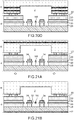
- a thin film of resin is applied by lamination to the underside of the cover 6 intended to come into contact with the layer 16 ( figure 16 ) or the intermediate layer 20 ( figures 17 and 18 ) and is structured by photolithography and development.
- the cover and resin film assembly is transferred and sealed to the substrate.
- the thin film 22 is in the form of two parallel beads, having substantially the same sealing surface. These cords are obtained after exposure and development of the dry film.
- the dry film is for example a resin with epoxy, phenol, acrylic or silicone bases for example.
- the dry film has, for example, a thickness of between a few ⁇ m to several tens of ⁇ m, or even a few hundred ⁇ m with a dry film multilayer, advantageously only a few ⁇ m.
- the sealing is advantageously carried out by dry film.
- the method which will be described allows the realization of several NEMS simultaneously in a fluidic channel aligned along the longitudinal axis, only one being visible. It will be understood that the method allows the production of several devices simultaneously with one or more NEMS, the devices then being separated at the end of the manufacturing process.
- the substrate provided with the NEMS / MEMS structure is produced from a silicon-on-insulator or SOl (Silicon Insulator) substrate for example.
- SOl Silicon Insulator
- any substrate comprising a layer in which the NEMS / MEMS structure would be produced, this layer being formed on a sacrificial layer allowing, by its etching, release of the NEMS / MEMS structure.
- the material of the layer in which the NEMS / MEMS structure is made can be a monocrystalline or polycrystalline semiconductor, for example. Si, Ge, SiGe, SiC, GAAs, InAs, InP, etc.
- the sacrificial layer may be present over the entire substrate or else be located only at certain places where the NEMS will be carried out.
- the NEMS / MEMS structure comprises an optical function so as to include opto-electro-mechanical microsystems (or MOEMS, for Micro-Opto-Electro-Mechanical Systems in English) and / or to integrate an integrated electronic part , CMOS, etc.
- opto-electro-mechanical microsystems or MOEMS, for Micro-Opto-Electro-Mechanical Systems in English
- MOEMS Micro-Opto-Electro-Mechanical Systems in English
- the first example of a method which will be described makes it possible to produce a device according to the invention comprising an intermediate layer and a localized functionalization layer with a level of interconnections at the level of the NEMS as for example shown in Figure figure 7 .
- the SOI substrate comprises a layer of insulating material 28, for example silicon oxide, and a silicon layer 30 in which the NEMS structure will be formed.
- the silicon of the layer 30 is doped.
- a protective oxide layer takes place, on the doped layer 30, for example it is a thermal oxide, then a step of implantation, then of annealing and deoxidation by removal of the oxide layer.
- the doping can be carried out full plate or with masking, for example by means of a resin if it is desired to locate areas with different doping.
- the NEMS structures and the electrical contact pads are defined.
- the element thus obtained is represented on the figure 19B .
- the figure 19B which is a sectional view only one NEMS is visible but preferably the structure has a plurality of NEMS in the X direction.
- the structure could also have several NEMS in a direction perpendicular to the X direction.
- the metal interconnection lines are made.
- a deposit of a dielectric layer 32 on the structured layer 30 then takes place, for example an oxide formed based on silane SiH 4 , the thickness of which is greater than the topology of the silicon layer. 30 structured.
- a chemical-mechanical or CMP polishing step then takes place in order to make the surface of the layer 32 flat.
- a photolithography of the "countermask” type and a partial etching of the layer 32 for the height of the topology to be made up. are carried out, which facilitates the polishing step and reduces its duration.
- the layer 32 is opened by photolithography and etching to reach the silicon layer 30 and prepare the production of the electrical contact pads and / or the interconnection lines between NEMS.
- a layer of metal 34 is deposited, for example in AISi, this having the advantage of offering good resistance to etching by vapor hydrofluoric acid which takes place to free the mechanical structures.
- the thicknesses of the layers formed are adapted to facilitate subsequent planarization.
- layer 32 is retained. As a variant, it could be removed, advantageously etched selectively with respect to the metal of the interconnection lines, in order to preserve the interconnection and / or metallization lines of the contact pads. It can be completely removed or only partially removed, for example in areas intended for assembly.
- the steps for making contact pads and / or interconnection lines can be repeated several times in order to achieve several levels of metallic interconnections. These steps can also make it possible to create electrical interconnection lines between different NEMS on one or more levels.
- the interconnection lines are then isolated from each other by the material of the layers 32.
- the intermediate layer 20 comprises two layers.
- a layer of dielectric material 35 is deposited, for example a silicon oxide formed based on silane SiH 4 , or else a silicon oxide formed based on tetraethylorthosilicate (TEOS).
- a protective layer 36 for example of amorphous Si, of silicon nitride, of metal (AISi, AlCu, etc.), of Hafnium oxide (HfO2), is then deposited on the layer 35, the latter increasing resistance to etching with hydrofluoric acid vapor used for the release of NEMS.
- the thickness of the intermediate layer in this case may for example be of the order of a few ⁇ m.
- the intermediate layer 20 is formed on metallic interconnect lines and / or electrical contact pads, but it could be implemented directly on the NEMS layer (with or without metallic interconnect lines or contact pads. contact), etc ... It should be noted that the layer 32 could have been removed after the formation of the interconnection lines, the intermediate layer 20 would then have been formed directly on them.
- a polishing step, for example by CMP, of the layer 32 prior to the deposition of the layer 20 can take place.
- the intermediate layer is etched so as to reach the NEMS / MEMS structure to be released.
- the amorphous Si layer 36 and the layer 35 are etched, the layer 32 can also be partially or totally etched.
- plasma etching based on SF 6 could be used for the amorphous Si layer and plasma etching based on CHF 3 for etching the silicon oxide forming the intermediate layer.
- the intermediate layer 20 can be etched in different ways to produce the different devices described above. It can thus be etched only above the sensitive parts while protecting the rest of the surface so that the intermediate layer is at the assembly interface and in the fluidic channel, or else only at the assembly interface or again only in the fluidic channel, in this case it only has an encapsulation function.
- the etching of the intermediate layer 20 is suitable for preserving both the metallic interconnections and the NEMS / MEMS structure in semiconductor material.
- the shape of the openings is determined for example by photolithography so as to take into account the length of release of the mechanical structures which occurs at the end of the “NEMS” process, because this step can cause an unwanted lateral etching of the planarizing layer of the intermediate layer 20, which, if it were not mastered, could lead to the release of unwanted areas such as metal interconnections, areas under the sealing interface with the cover.
- the etching of the opening in the intermediate layer is preferably stopped at the level of the metal layer above the semiconductor, before reaching the semiconductor, so as not to damage the semiconductor layer. conductor which constitutes the mechanical structure.
- the NEMS / MEMS structure in particular the mobile part or parts 10, is / are released.
- the release takes place, for example, by isotropic etching using vapor hydrofluoric acid of the dielectric materials surrounding the NEMS structure, these are layers 28 and 32.
- Layer 28 can be totally or partially etched. Due to the presence of the protective layer 36, the layer 35 is protected, its thickness does not decrease.
- FIG 19H is represented the element of the figure 19G comprising a localized functionalization layer 118 on the suspended part 10 of the NEMS.
- this layer could be non-localized.
- This functionalization layer can be produced in different ways by liquid or gas phase deposits.
- gas phase deposition techniques for example by chemical vapor deposition or CVD (Chemical Vapor Deposition), by LPCVD, by PECVD, by deposition of thin atomic layers or ALD (Atomic Layer Deposition) ), etc. are used.
- Techniques for epitaxy and / or porosification of materials and / or of the evaporation type can also be implemented. These techniques are preferable to liquid techniques, spray or spotting type (depositing drops), because they make it possible to avoid the use of liquid phases in the presence of released NEMS structures. However, these latter techniques can also be used, for example if the NEMS / MEMS structures are sufficiently rigid.
- the deposited materials forming the functionalization layer (s) can be, for example, materials of polymer type, dielectrics, semiconductors or other porous materials, metals, and the like.
- the functionalization layer is represented only on the surface of the NEMS.
- the functionalization layer surrounds the NEMS, the thickness of the functionalization layer not necessarily being uniform all around the mechanical structure.
- This deposition is obtained by implementing conformal deposition techniques, for example by CVD.
- cover substrate 38 An example of steps for producing the cover 6 will now be described on the basis of a substrate 38 polished on both sides, for example made of silicon, glass, quartz, etc., designated cover substrate 38.
- marks are defined and then etched on the rear face 38.1 and on the front face 38.2 of the substrate, these marks serving for the alignment between the NEMS substrate and the cover during their sealing.
- a deposition of a hard mask for example of a silicon oxide mask a few ⁇ m thick, is carried out on the front face 38.2 of the substrate 38 ( figure 20A ). Photolithography and etching of the mask 40 take place to define the cavities.
- the cover substrate 38 is etched for example by deep reactive ionic etching or DRIE (Deep reactive ionic etching in English) with for example a process of the "Bosch" type consisting of a succession of etching steps with an SF 6 plasma and passivation with a C 4 F 8 plasma thus forming the cavities which will delimit the fluidic channels.
- DRIE Deep reactive ionic etching in English
- the depth of the etching is for example of the order of a few hundred ⁇ m.
- the hard mask can then be removed, for example by wet etching of the HF type.
- Two lithography steps can be carried out if it is desired to obtain several engraving depths, for example a first depth for the fluidic channel and a second depth to produce the inlet (s) and the outlet (s) of the fluidic channel.
- the materials may be those of the functionalization layer of the NEMS structure or other materials.
- the cover on the substrate, by a dry film of resin.
- the dry film is formed on the cover.
- the cover 6 is prepared for sealing on the NEMS / MEMS structure by means of a dry film.
- the sealing surface of the cover is prepared so as to ensure good adhesion of the dry film on the cover.
- the dry film 22 is then fixed to the front face 38.2 of the cover substrate 38, this fixing is advantageously obtained by lamination. This rolling makes it possible to work despite the strong topology due to the existence of the fluidic channels on this side of the substrate.
- lithography and development are carried out to structure the dry film, the latter then having beads along the cavities engraved in the cover. It may be a wide bead, or then preferably several narrow cords parallel to each other as shown in the figure. figure 20C . In the latter case, for example the cords and the spaces between the cords may be from a few ⁇ m to a few tens of micrometers.
- the cords have a regular structure and a close sealing surface over the entire structure to be sealed so as to ensure homogeneous crushing of the dry film with reasonable pressure during the sealing step.
- the cover substrate 38 is then ready to be sealed on the substrate of the NEMS / MEMS 4 structure.
- sealing techniques can be implemented to assemble the cover and the substrate.
- other preparation steps can be implemented, for example specific cleaning.
- sealing techniques known to those skilled in the art can be implemented, such as for example molecular sealing or even eutectic seals, metal seals, for example by thermocompression, some of these seals possibly requiring the prior formation of cords. metallic.
- the cover 6 and the substrate 4 comprising the NEMS / MEMS structure are sealed.
- the sealing is carried out on a sealing equipment which makes it possible to control the temperature and the pressure applied between the cover and the substrate to be sealed.
- Surface treatments known in the state of the art can optionally be carried out to optimize the bonding energy.
- the substrate 4 and the cover 6 are aligned by means of the marks made previously on the substrates.
- the pressure applied is of the order of a few kN to a few tens of kN, and for example the temperature is between 100 ° C and 200 ° C.
- the substrate 4 and the cover 6 are then assembled.
- the fluidic channel is then sealed at the lateral edges.
- an assembly such as that of the figure 20D is made from circular substrates used in microelectronics.
- the silicon substrate on the rear face is thinned, for example by grinding and then by chemical-mechanical polishing.
- the depth of the vias is advantageously limited and the operations for filling the cavities with the metal are facilitated.
- the remaining thickness of the substrate is such that a sufficient thickness is retained to maintain a non-weakened assembly.
- the substrate on the rear face has a remaining thickness of the order of 15 ⁇ m to 50 ⁇ m, for vias a few ⁇ m wide, for example 5 ⁇ m. This width makes it possible to have a high density of contacts. With the form factors of the order of 2 to 10, the depths of the vias are then approximately 10 to 50 ⁇ m. These dimensions allow both a high density of vias and preserve a layer thickness of the substrate remaining after thinning sufficient for the region of the substrate forming the lower bottom of the fluidic channel to withstand thinning operations.
- the fluidic channel may for example have a few tens of ⁇ m to a few hundred ⁇ m, typically 100 ⁇ m in depth for 100 ⁇ m in width.
- the thinning step takes place after the step of sealing the cover and the NEMS substrate, so that the cover serves as a “handle” during thinning operations of the NEMS substrate.
- the cover serves as a “handle” during thinning operations of the NEMS substrate.
- the thinning step can be carried out by chemical etching, plasma etching, etc.
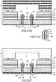
- a layer of dielectric material 42 is formed on the rear face, for example with a thickness of a few ⁇ m.
- Layer 42 is for example silicon oxide deposited by PECVD for example.
- the purpose of this layer 42 is to isolate the vias from a redistribution part, also called RDL for “Redistribution Layer” in English terminology, which will be combined during a subsequent step in order to connect the device comprising vias to an external electronic circuit.
- RDL redistribution part
- the vias are produced in the thinned substrate.
- the layer 42 is structured, for example by lithography and anisotropic etching, for example by CHF 3 plasma. Then the silicon substrate 27 is etched for example by DRIE plasma SF 6 and passivation C 4 F 8 and the sacrificial layer 28 is also etched, for example by plasma CHF 3 , with etching stop on the NEMS layer 30.
- the holes thus trained are designated 44.
- a first deep etching is carried out with stopping in the oxide layer 28 and then a fine etching is carried out to reach the layer 30 and avoid damaging it.
- the resin is then removed.
- etching processes are advantageously chosen in order to avoid under-etching and the effects of scalloping along the walls.
- the dimensions of the holes are for example of the order of 2 ⁇ m to 10 ⁇ m wide and 10 ⁇ m to 100 ⁇ m deep. These dimensions allow stages of engraving, cleaning of the via bottoms, compliance of the filling materials, etc ...
- the engraving could be carried out by laser drilling, but the stopping on the layer 30 can be more complex.
- a layer of electrically insulating material 46 is formed on the inner face of the holes 44, for example by depositing the material advantageously exhibiting very good conformity, for example it is an SiO 2 dielectric. formed by SACVD (Sub-atmospheric Chemical Vapor Deposition in English terminology) of a few hundred nm, to achieve the lateral electrical insulation of holes 44.
- SACVD Sub-atmospheric Chemical Vapor Deposition in English terminology
- electrical insulation materials can be used, for example other types of SiO 2 and other dielectrics, for example a polymer.
- the holes 144 are covered with a layer of electrically insulating material 146.
- the engraving described in relation to the figure 21B stops in the sacrificial layer 28 which reduces the risk of deterioration of the NEMS layer, which is thin with regard to the thickness etched in the substrate. Then, the electrical insulation layer is deposited and the etching is resumed to reach the NEMS layer 30.
- a barrier layer (not shown) is then formed at the bottom of the hole and on the side walls of the holes, for example made of TiN, Ti, Ta, TaN, etc., for example of a few tens of 10 nm. This is for example deposited by spraying or CVD ....
- a seed layer is formed, for example of copper by PVD and / or CDV and / or sputtering in order to prepare the filling of the via with a metal.
- This layer has for example a thickness between a few tens of nm and a few hundred nm.
- the holes are filled with an electrically conductive material 48, so as to form vias.
- the electrically conductive material is metallic, for example in Cu, in W, in highly doped polysilicon Si, for example.
- the filling is carried out for example by electrochemical deposition or ECD (ElectroChemical Deposition). Thermal annealing can then take place.
- ECD ElectroChemical Deposition
- the filling can also be carried out by CVD or PVD, these techniques making it possible to ensure good conformity of the filling.
- a mechanical-chemical polishing step then has to planarize the whole and remove the excess Cu.
- the electrically conductive material of the via is in contact with the silicon of the NEMS, for example it is a Cu / Si or W / Si contact.
- the conductive material 148 is in contact with the metal present at the surface of the contact pad or of the interconnection line, for example it is a Cu / Cu or Cu / AISi contact.
- a distribution layer or RDL can be formed on the surface where the vias open, for example by implementing the following steps: For example, a thin layer 50 of SiN nitride is formed on the rear face, for example having a thickness of the order of 50 nm, as well as a layer of RDL insulation oxide 52 with a thickness of a few hundred nm. on layer 50.
- a lithography on the layer 52 and an etching of the RDL oxide 52 take place with stopping on the layer 52, so as to form lines 54 etched in the RDL oxide.
- the resin is removed.
- a metallization of the bottom of the lines takes place, for example with a layer of TiN and copper.
- This metallization is for example carried out by PVD over a thickness of a few hundred nm, then the lines are filled with copper 56 deposited for example by ECD, for example over a thickness of 1 ⁇ m. Then take place an annealing and mechanical-chemical polishing.
- the RDL layer makes it possible to distribute the TSV contacts and prepare the device for connection with the outside, for example with an integrated circuit.
- this layer can be used to perform electrical tests to sort the chips if need before assembling them with the integrated circuit, which makes it possible to optimize the costs by taking into account the efficiency aspects if these are different for the devices of the invention and the integrated circuits.
- the device could be prepared in a known manner for connection with integrated circuits (chips or wafers).
- connection operations of the devices to integrated circuits thanks to operations of the chip transfer or wafer transfer type, by connecting the vias of the device of the invention to one of the metal levels of the circuit (s). ) integrated, advantageously via the RDL layer.
- This operation can be carried out in different ways by transferring a wafer to another wafer (“Wafer to Wafer”), or chips to a wafer (“Die to Wafer”) or even chips to chips (“Die to Die “).
- Wafer to Wafer a wafer to another wafer
- Die to Wafer chips to a wafer
- Dies to Die chips to chips
- the chips forming an integrated circuit can be transferred to chips or wafers of devices of the invention or else the reverse.
- an intermediate layer 20 was produced on the substrate comprising the NEMS before sealing to the cover.
- the device according to the invention may not include an intermediate layer.
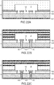
- the steps of making the vias in a device without an intermediate layer we can see the steps of making the vias in a device without an intermediate layer.
- the steps for producing the substrate comprising the NEMS are similar to the steps shown on the figures 19A and 19B . In this example there is no realization of interconnection lines.
- the sealing is carried out in a similar manner to the sealing of the step shown on the figure 20C .
- It is preferably a dry film seal, but it can alternatively be a eutectic seal, a molecular seal, a metal seal by thermocompression, etc.
- the substrate 4 is thinned on the rear face, for example by grinding then CMP, in order to achieve a thickness for example between 15 ⁇ m and 50 ⁇ m.
- a layer 57 of a dielectric material is formed on the rear face.
- holes 58 are etched in the substrate according to the method described in relation to the figure 21C .
- the etching can stop on the NEMS 30 layer.
- a layer of electrically insulating material 60 for example SiO 2 SACVD is deposited on the inner face of the holes according to the method described in relation to the figure 21D .
- the vias are formed by filling the holes with an electrically conductive material 62, preferably a metal, according to the method described in relation to the figure 21E .
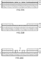
- the first stages of making the NEMS substrate are similar to the stages of figures 19A and 19B .
- an intermediate layer 20 is formed on the layer 30. It can be formed of several materials, for example it can comprise on the surface a layer resistant to the etching of release of the NEMS, for example it can be made of silicon. amorphous resistant to hydrofluoric acid vapor.
- the intermediate layer 20 is structured in order to access the area of the NEMS structure (s) to be released. For this, lithography and etching of the intermediate layer 20 take place.
- the intermediate layer 20 is kept in the assembly area. It could be structured otherwise as has been described above, for example only above the sensitive parts while protecting the rest of the surface or else to etch at the assembly interface to remove the intermediate layer in this. area and keep it only in the fluidic channel.
- the NEMS structure is released, for example by hydrofluoric acid vapor.
- the sealing is carried out in a similar manner to the sealing of the step shown on the figure 20C .
- It is preferably a dry film seal, but it can alternatively be a eutectic seal, a molecular seal, by thermocompression, etc.
- the sealing takes place between the intermediate layer 20 and the cover 6.
- the element thus obtained is shown in FIG. figure 23D .
- the substrate 4 is thinned on the rear face, for example by grinding then CMP, in order to achieve a thickness for example between 15 ⁇ m and 50 ⁇ m.
- a layer 62 of a dielectric material is formed on the rear face.
- holes 64 are etched in the substrate according to the method described in relation to the figure 21C .
- the etching can stop on the NEMS 30 layer ( figure 23E ), or in the sacrificial layer 28.
- a layer of electrically insulating material 66 for example SiO 2 SACVD is deposited on the inner face of the holes according to the method described in relation to the figure 21D .
- the vias are formed by filling the holes with an electrically conductive material 38, preferably a metal.
- the vias are produced after sealing the cover on the NEMS substrate and after release of the NEMS.
- the devices according to the invention could be produced with methods in which the vias would be produced before release of the NEMS and before the sealing of the cover on the NEMS substrate or after the release of the NEMS and before the sealing between the cover and the NEMS substrate. .
- the stages of separating the device chips can be carried out before or after sealing with the integrated circuits.
- a fluidic channel device comprising one or more mechanical structures suspended in the channel, thus avoiding the formation of via in the cover and / or at the sealing interface and lines. side interconnections making it more complex to achieve the seal between the cover and the NEMS substrate.
- the invention makes it possible to easily produce networks of mechanical structures by allowing a dense and complex electrical interconnection as close as possible to the mechanical structures, possibly with several levels of metal.
- the invention can also make it possible to encapsulate all the structures and layers present in the channel except the sensitive structures with an encapsulation layer. Finally, it allows the implementation of functionalization during the process on suspended mechanical structures.
Landscapes
- Engineering & Computer Science (AREA)
- Microelectronics & Electronic Packaging (AREA)
- Manufacturing & Machinery (AREA)
- Chemical & Material Sciences (AREA)
- Computer Hardware Design (AREA)
- Health & Medical Sciences (AREA)
- Analytical Chemistry (AREA)
- Biochemistry (AREA)
- General Health & Medical Sciences (AREA)
- General Physics & Mathematics (AREA)
- Immunology (AREA)
- Pathology (AREA)
- Life Sciences & Earth Sciences (AREA)
- Physics & Mathematics (AREA)
- Nanotechnology (AREA)
- Micromachines (AREA)
Claims (15)
- Vorrichtung, umfassend ein Substrat, das wenigstens eine mikroelektronische und/oder nanoelektronische Struktur (NEMS) umfasst, umfassend wenigstens einen empfindlichen Teil und einen Fluidkanal (2), der zwischen dem Substrat und einer Kappe (6) definiert ist, wobei der Fluidkanal (2) wenigstens zwei Öffnungen zum Sicherstellen einer Zirkulation in dem Kanal umfasst, wobei die mikroelektronische und/oder nanoelektronische Struktur im Inneren des Fluidkanals angeordnet ist, wobei die Kappe mit dem Substrat im Bereich einer Zusammenfügungsgrenzfläche zusammengefügt ist, wobei die Vorrichtung wenigstens eine elektrische Verbindung zwischen der mikroelektronischen und/oder nanoelektronischen Struktur und dem Äußeren des Fluidkanals (2) umfasst, wobei die elektrische Verbindung (8) durch eine Durchführung gebildet ist, die durch das Substrat (4) lotrecht zu der mikroelektronischen und/oder nanoelektronischen Struktur und im elektrischen Kontakt mit der mikroelektronischen und/oder nanoelektronischen Struktur realisiert ist, wobei die Vorrichtung ferner eine Funktionalisierungsschicht (18, 118) umfasst, die wenigstens einen Teil des empfindlichen Teils der mikroelektronischen und/oder nanoelektronischen Struktur bedeckt.
- Vorrichtung nach Anspruch 1, bei der die Durchführung in elektrischem Kontakt mit der mikroelektronischen und/oder nanoelektronischen Struktur mittels eines Kontaktpunkts ist, der in dem Fluidkanal angeordnet ist.
- Vorrichtung nach Anspruch 1 oder 2, ferner umfassend eine Zwischenschicht (120, 220), die wenigstens teilweise in dem Fluidkanal angeordnet ist, und die unter einem Teil der Funktionalisierungsschicht (18, 118) angeordnet ist, wobei die Zwischenschicht (120, 220) in dem Fluidkanal (2) wenigstens teilweise die mikroelektronische und/oder nanoelektronische Struktur bedeckt, mit Ausnahme ihres empfindlichen Teils.
- Vorrichtung nach Anspruch 3, bei der die Zwischenschicht (20) eine Einkapselungsschicht ist, und/oder bei der die Zwischenschicht (20, 120, 220) ein elektrisch isolierendes Material umfasst, beispielsweise ein Siliziumoxid oder ein Siliziumnitrid, wobei die Zwischenschicht (120, 220) vorzugsweise die Verbindungsleitungen elektrisch isoliert.
- Vorrichtung nach einem der Ansprüche 1 bis 4, umfassend mehrere mikroelektronische und/oder nanoelektronische Strukturen, die in dem Fluidkanal miteinander verbunden sind, wobei die mikroelektronischen und/oder nanoelektronischen Strukturen vorzugsweise durch Verbindungsleitungen miteinander verbunden sind, die in dem Fluidkanal angeordnet sind.
- Vorrichtung nach einem der Ansprüche 1 bis 5, umfassend einen trockenen Versiegelungsfilm (22), der zwischen dem Substrat (4) und der Kappe eingefügt ist, wobei der trockene Versiegelungsfilm (22) vorzugsweise mehrere Bänder umfasst, oder wobei die Vorrichtung wenigstens eine Materialschicht umfasst, die zwischen dem Substrat und der Kappe (6) eingefügt ist, die eine eutektische oder metallische Versiegelung oder mittels Thermokompression realisiert, oder mittels Siebdruck oder eine molekulare Versiegelung oder eine Versiegelung mittels Glassinterung.
- Vorrichtung nach einem der Ansprüche 1 bis 6, bei der der Kanal eine Gasphasenchromatographie-Mikrosäule bildet.
- Verfahren zur Herstellung wenigstens einer Vorrichtung nach einem der Ansprüche 1 bis 7, umfassend die Schritte:a) Realisieren wenigstens einer mikroelektronischen und/oder nanoelektronischen Struktur auf einem Substrat,b) Realisieren einer Kappe (6), die einen Fluidkanal (2) umfasst, in einem Kappensubstrat,d) Versiegeln der Kappe (6) und des Substrats derart, dass die mikroelektronische und/oder nanoelektronische Struktur in dem Fluidkanal (2) angeordnet ist,e) Realisieren wenigstens einer Durchführung in dem Substrat lotrecht zu der mikroelektronischen und/oder nanoelektronischen Struktur,wobei der Schritt e) nach dem Schritt d) oder vor dem Schritt d) erfolgen kann,wobei das Verfahren ferner zwischen dem Schritt b) und dem Schritt d) umfasst:
c) Realisieren einer Funktionalisierungsschicht (18, 118) im Inneren des Fluidkanals (2) auf der mikroelektronischen und/oder nanoelektronischen Struktur, wobei die Funktionalisierungsschicht ferner auf den Wänden der Kappe (6) sein kann, wobei die Funktionalisierungsschicht (18, 118) vor der Versiegelung realisiert wird. - Verfahren nach Anspruch 8, bei dem die Realisierung der Durchführung wenigstens umfasst:- den Schritt der Realisierung eines Lochs wenigstens in einem Teil des Substrats,- den Schritt des Füllens des gesamten Lochs oder eines Teils davon mit einem elektrisch leitenden Material,wobei das Verfahren vorzugsweise vor der Realisierung der wenigstens einen Durchführung und nach dem Schritt d) einen Schritt des Abdünnens des Substrats umfasst.
- Verfahren nach Anspruch 9, umfassend vor dem Schritt des Füllens des Lochs mit einem elektrisch leitenden Material einen Schritt des Aufbringens eines elektrisch isolierenden Materials auf die Innenoberfläche des Lochs.
- Verfahren nach Anspruch 9 oder 10, bei dem die Realisierung des Lochs durch ein Tiefätzen und anschließend durch ein Feinätzen erzielt wird, und/oder bei dem der empfindliche Teil der mikroelektronischen und/oder nanoelektronischen Struktur aufgehängt ist und dieser vor dem Schritt d) freigesetzt wird.
- Verfahren nach einem der Ansprüche 8 bis 11, umfassend einen Schritt des Bildens einer Zwischenschicht auf dem Substrat nach dem Schritt a) in einer Zone derart, dass sie wenigstens einen in dem Fluidkanal angeordneten Teil umfasst, nach dem Schritt e), oder einen Schritt des Bildens einer Zwischenschicht auf dem Substrat nach dem Schritt a) in einer Zone derart, dass sie sich ausschließlich bei der Zusammenfügungsgrenzfläche befindet, nach dem Schritt e), wobei die Funktionalisierungsschicht vorzugsweise auf der Zwischenschicht gebildet wird.
- Verfahren nach einem der Ansprüche 8 bis 12, umfassend während des Schritts a) die Realisierung, in der mikroelektronischen und/oder nanoelektronischen Struktur, wenigstens eines elektrischen Kontaktpunkts, der dazu ausgelegt ist, einen elektrischen Kontakt mit der Durchführung sicherzustellen, wobei das Verfahren vorzugsweise zur Bildung des Kontaktpunkts eine zusätzliche metallische Abscheidung auf diesem umfasst.
- Verfahren zur Herstellung nach einem der Ansprüche 8 bis 13, bei dem der Versiegelungsschritt einen trockenen Film verwendet, wobei das Herstellungsverfahren die folgenden Teilschritte umfasst:- Laminieren des trockenen Films auf die Basisflächen der Wände der Kappe,- Strukturieren des trockenen Films,- Annähern der Kappe und des Substrats, umfassend die mikroelektronische(n) und/oder nanoelektronische(n) Struktur(en),- Ausüben eines Drucks derart, dass der trockene Film zerdrückt wird, oderbei dem die Versiegelung eine eutektische oder metallische Versiegelung mittels Thermokompression ist, oder durch molekulare Versiegelung oder durch Siebdruck.
- Verfahren zur Herstellung nach einem der Ansprüche 8 bis 14, bei dem mehrere Vorrichtungen gleichzeitig realisiert werden, wobei das Substrat mehrere mikroelektronische und/oder nanoelektronische Strukturen umfasst und das Kappensubstrat mehrere Kappen umfasst, wobei die Kappen gleichzeitig auf dem Substrat versiegelt werden, das die mikroelektronischen und/oder nanoelektronischen Strukturen umfasst, derart, dass ein Fluidkanal einer Vorrichtung wohl oder nicht mit dem Fluidkanal von anderen Vorrichtungen kommunizieren kann, wobei das Verfahren die Schritte umfassen kann:- Realisieren von Vorausschneidungen in einer Richtung orthogonal zu den Fluidkanälen in dem Kappensubstrat und in dem Substrat,- Separieren der Vorrichtungen, vorzugsweise durch Spaltung,- Vorausschneiden oder Ausschneiden in einer Richtung parallel zu den Fluidkanälen zwischen den Kanälen,- Separieren der Vorrichtungen, vorzugsweise durch Spalten der Vorausschneidungen.
Applications Claiming Priority (2)
| Application Number | Priority Date | Filing Date | Title |
|---|---|---|---|
| FR1357200A FR3008691B1 (fr) | 2013-07-22 | 2013-07-22 | Dispositif comportant un canal fluidique muni d'au moins un systeme micro ou nanoelectronique et procede de realisation d'un tel dispositif |
| EP14177871.2A EP2829509B1 (de) | 2013-07-22 | 2014-07-21 | Vorrichtung mit einem Fluidkanal ausgestattet mit mindestens einem mikro- oder nanoelektronischen System und Herstellungsverfahren einer solchen Vorrichtung |
Related Parent Applications (1)
| Application Number | Title | Priority Date | Filing Date |
|---|---|---|---|
| EP14177871.2A Division EP2829509B1 (de) | 2013-07-22 | 2014-07-21 | Vorrichtung mit einem Fluidkanal ausgestattet mit mindestens einem mikro- oder nanoelektronischen System und Herstellungsverfahren einer solchen Vorrichtung |
Publications (2)
| Publication Number | Publication Date |
|---|---|
| EP3702323A1 EP3702323A1 (de) | 2020-09-02 |
| EP3702323B1 true EP3702323B1 (de) | 2021-10-06 |
Family
ID=49620064
Family Applications (2)
| Application Number | Title | Priority Date | Filing Date |
|---|---|---|---|
| EP14177871.2A Active EP2829509B1 (de) | 2013-07-22 | 2014-07-21 | Vorrichtung mit einem Fluidkanal ausgestattet mit mindestens einem mikro- oder nanoelektronischen System und Herstellungsverfahren einer solchen Vorrichtung |
| EP20171331.0A Not-in-force EP3702323B1 (de) | 2013-07-22 | 2014-07-21 | Vorrichtung, die einen mit mindestens einem mikro- oder nanoelektronischen system ausgestatteten fluidkanal umfasst, und herstellungsverfahren einer solchen vorrichtung |
Family Applications Before (1)
| Application Number | Title | Priority Date | Filing Date |
|---|---|---|---|
| EP14177871.2A Active EP2829509B1 (de) | 2013-07-22 | 2014-07-21 | Vorrichtung mit einem Fluidkanal ausgestattet mit mindestens einem mikro- oder nanoelektronischen System und Herstellungsverfahren einer solchen Vorrichtung |
Country Status (4)
| Country | Link |
|---|---|
| US (1) | US9340410B2 (de) |
| EP (2) | EP2829509B1 (de) |
| CN (1) | CN104326435B (de) |
| FR (1) | FR3008691B1 (de) |
Families Citing this family (10)
| Publication number | Priority date | Publication date | Assignee | Title |
|---|---|---|---|---|
| WO2011154363A2 (en) * | 2010-06-07 | 2011-12-15 | Commissariat à l'énergie atomique et aux énergies alternatives | Analysis device including a mems and/or nems network |
| FR2973944B1 (fr) | 2011-04-06 | 2014-01-10 | Commissariat Energie Atomique | Emetteur pour systeme thermophotovoltaique et systeme thermophotovoltaique comportant au moins un tel emetteur |
| FR2986908B1 (fr) | 2012-02-14 | 2014-03-28 | Commissariat Energie Atomique | Dispositif de recuperation et de conversion d'energie thermique en energie electrique |
| FR2999335B1 (fr) | 2012-12-06 | 2016-03-11 | Commissariat Energie Atomique | Procede ameliore de realisation d'un composant a structure suspendue et d'un transistor co-integres sur un meme substrat. |
| FR3002219B1 (fr) | 2013-02-19 | 2015-04-10 | Commissariat Energie Atomique | Procede de fabrication d'une structure micromecanique et/ou nanomecanique comportant une surface poreuse |
| FR3008690B1 (fr) * | 2013-07-22 | 2016-12-23 | Commissariat Energie Atomique | Dispositif comportant un canal fluidique muni d'au moins un systeme micro ou nanoelectronique et procede de realisation d'un tel dispositif |
| FR3011835B1 (fr) | 2013-10-16 | 2015-12-25 | Commissariat Energie Atomique | Procede de realisation par voie electrochimique d'au moins une zone poreuse d'une structure micro et/ou nanoelectronique |
| US9630835B2 (en) * | 2014-08-25 | 2017-04-25 | Texas Instruments Incorporated | Wafer level packaging of MEMS |
| US11364493B2 (en) * | 2017-10-12 | 2022-06-21 | Hewlett-Packard Development Company, L.P. | Planarization layers over silicon dies |
| CN107758604B (zh) * | 2017-11-03 | 2024-07-19 | 纽威仕微电子(无锡)有限公司 | Mems水听器芯片的扇出型封装结构及方法 |
Family Cites Families (19)
| Publication number | Priority date | Publication date | Assignee | Title |
|---|---|---|---|---|
| US6548895B1 (en) | 2001-02-21 | 2003-04-15 | Sandia Corporation | Packaging of electro-microfluidic devices |
| TW560018B (en) * | 2001-10-30 | 2003-11-01 | Asia Pacific Microsystems Inc | A wafer level packaged structure and method for manufacturing the same |
| US7098117B2 (en) * | 2002-10-18 | 2006-08-29 | The Regents Of The University Of Michigan | Method of fabricating a package with substantially vertical feedthroughs for micromachined or MEMS devices |
| IL165948A0 (en) * | 2004-12-23 | 2006-01-15 | Rafael Armament Dev Authority | Chip packaging |
| US7553695B2 (en) * | 2005-03-17 | 2009-06-30 | Hymite A/S | Method of fabricating a package for a micro component |
| US20070013014A1 (en) * | 2005-05-03 | 2007-01-18 | Shuwen Guo | High temperature resistant solid state pressure sensor |
| JP5174673B2 (ja) * | 2005-10-14 | 2013-04-03 | エスティーマイクロエレクトロニクス エス.アール.エル. | 基板レベル・アセンブリを具えた電子装置及びその製造処理方法 |
| DE102008025599B4 (de) * | 2007-05-14 | 2013-02-21 | Fraunhofer-Gesellschaft zur Förderung der angewandten Forschung e.V. | Gehäuste aktive Mikrostrukturen mit Direktkontaktierung zu einem Substrat |
| FR2948114B1 (fr) | 2009-07-17 | 2012-03-30 | Commissariat Energie Atomique | Nems comportant des moyens de transduction a base d'alliage d'aluminium |
| WO2011154363A2 (en) | 2010-06-07 | 2011-12-15 | Commissariat à l'énergie atomique et aux énergies alternatives | Analysis device including a mems and/or nems network |
| US9184099B2 (en) * | 2010-10-04 | 2015-11-10 | The Board Of Trustees Of The Leland Stanford Junior University | Biosensor devices, systems and methods therefor |
| US20120126433A1 (en) * | 2010-11-19 | 2012-05-24 | Baolab Microsystems Sl | Methods and systems for fabrication of mems cmos devices in lower node designs |
| DE102011005676A1 (de) * | 2011-03-17 | 2012-09-20 | Robert Bosch Gmbh | Bauteil |
| FR2973944B1 (fr) | 2011-04-06 | 2014-01-10 | Commissariat Energie Atomique | Emetteur pour systeme thermophotovoltaique et systeme thermophotovoltaique comportant au moins un tel emetteur |
| FR2977121B1 (fr) | 2011-06-22 | 2014-04-25 | Commissariat Energie Atomique | Systeme de gestion thermique a materiau a volume variable |
| FR2986908B1 (fr) | 2012-02-14 | 2014-03-28 | Commissariat Energie Atomique | Dispositif de recuperation et de conversion d'energie thermique en energie electrique |
| US8889451B2 (en) * | 2012-02-21 | 2014-11-18 | Freescale Semiconductor, Inc. | MEMS pressure transducer assembly and method of packaging same |
| FR2999335B1 (fr) | 2012-12-06 | 2016-03-11 | Commissariat Energie Atomique | Procede ameliore de realisation d'un composant a structure suspendue et d'un transistor co-integres sur un meme substrat. |
| US20140264647A1 (en) * | 2013-03-15 | 2014-09-18 | Rakesh Katragadda | Method of forming monolithic cmos-mems hybrid integrated, packaged structures |
-
2013
- 2013-07-22 FR FR1357200A patent/FR3008691B1/fr not_active Expired - Fee Related
-
2014
- 2014-07-21 EP EP14177871.2A patent/EP2829509B1/de active Active
- 2014-07-21 EP EP20171331.0A patent/EP3702323B1/de not_active Not-in-force
- 2014-07-21 US US14/336,351 patent/US9340410B2/en active Active
- 2014-07-22 CN CN201410351867.1A patent/CN104326435B/zh active Active
Also Published As
| Publication number | Publication date |
|---|---|
| FR3008691B1 (fr) | 2016-12-23 |
| FR3008691A1 (fr) | 2015-01-23 |
| EP2829509A1 (de) | 2015-01-28 |
| US20150021720A1 (en) | 2015-01-22 |
| US9340410B2 (en) | 2016-05-17 |
| CN104326435A (zh) | 2015-02-04 |
| EP2829509B1 (de) | 2020-04-29 |
| EP3702323A1 (de) | 2020-09-02 |
| CN104326435B (zh) | 2018-06-05 |
Similar Documents
| Publication | Publication Date | Title |
|---|---|---|
| EP3702323B1 (de) | Vorrichtung, die einen mit mindestens einem mikro- oder nanoelektronischen system ausgestatteten fluidkanal umfasst, und herstellungsverfahren einer solchen vorrichtung | |
| EP2829511B1 (de) | Vorrichtung, die einen mit mindestens einem mikro- oder nanoelektronischen System ausgestatteten Fluidkanal umfasst, und Herstellungsverfahren einer solchen Vorrichtung | |
| EP2863420B1 (de) | Verbessertes Verfahren zum Zusammenbau durch direktes Bonden von zwei Elementen, wobei jedes Element Metallanteile und Anteile aus dielektrischem Material umfasst | |
| EP2192612B1 (de) | Verfahren zum Stapeln und Vernetzen von integrierten Schaltkreisen | |
| US20120256308A1 (en) | Method for Sealing a Micro-Cavity | |
| CN101295653A (zh) | 半导体元件的制造方法 | |
| FR2992467A1 (fr) | Procede de realisation d'un composant a contact electrique traversant et composant obtenu | |
| EP2546188B1 (de) | Verfahren zur Herstellung einer Struktur mit einer aufgehängten Membran und einer vergrabenen Elektrode | |
| WO2021099713A1 (fr) | Procede de fabrication d'une puce fonctionnelle adaptee pour etre assemblee a des elements filaires | |
| FR2990297A1 (fr) | Empilement de structures semi-conductrices et procede de fabrication correspondant | |
| CN102214662A (zh) | 非制冷红外焦平面阵列探测器单片集成结构及制作方法 | |
| FR2980036A1 (fr) | Procede de realisation d'une structure integree tridimensionnelle et structure correspondante | |
| EP2661413B1 (de) | Verfahren zum einkapseln einer mikrokomponente | |
| EP3159302B1 (de) | Einkapselungsverfahren eines mikroelektronischen bauteils | |
| EP3035378B1 (de) | Umwandlungsverfahren einer elektronischen vorrichtung verwendbar in einem verfahren des temporären bondens eines wafers auf ein trägersubstrat und elektronische vorrichtung hergestellt durch das verfahren | |
| EP2162908B1 (de) | Herstellungsverfahren eines rekonstituierten elektronischen bauelements und entsprechendes rekonstituiertes elektronisches bauelement | |
| EP4505512B1 (de) | Substrat mit vias und zugehörige herstellungsverfahren | |
| FR2901636A1 (fr) | Connecteur a vias isoles | |
| EP4268277B1 (de) | Vorrichtung mit einem halbeingebetteten schaft für einen elektrischen verbindungseinsatz | |
| FR2999017A1 (fr) | Structure integree tridimensionnelle a dissipation thermique amelioree | |
| FR3074358A1 (fr) | Procede de realisation d'une cavite etanche a couche mince | |
| FR3044165A1 (fr) | Realisation d'interconnexions par recourbement d'elements conducteurs sous un dispositif microelectronique tel qu'une puce | |
| WO2008012481A1 (fr) | Procédé de fabrication d'un circuit intégré encapsulé et circuit intégré encapsulé associé | |
| FR2978610A1 (fr) | Procede de realisation d'une liaison electriquement conductrice traversante et dispositif integre correspondant |
Legal Events
| Date | Code | Title | Description |
|---|---|---|---|
| PUAI | Public reference made under article 153(3) epc to a published international application that has entered the european phase |
Free format text: ORIGINAL CODE: 0009012 |
|
| STAA | Information on the status of an ep patent application or granted ep patent |
Free format text: STATUS: REQUEST FOR EXAMINATION WAS MADE |
|
| 17P | Request for examination filed |
Effective date: 20200424 |
|
| AC | Divisional application: reference to earlier application |
Ref document number: 2829509 Country of ref document: EP Kind code of ref document: P |
|
| AK | Designated contracting states |
Kind code of ref document: A1 Designated state(s): AL AT BE BG CH CY CZ DE DK EE ES FI FR GB GR HR HU IE IS IT LI LT LU LV MC MK MT NL NO PL PT RO RS SE SI SK SM TR |
|
| GRAP | Despatch of communication of intention to grant a patent |
Free format text: ORIGINAL CODE: EPIDOSNIGR1 |
|
| STAA | Information on the status of an ep patent application or granted ep patent |
Free format text: STATUS: GRANT OF PATENT IS INTENDED |
|
| INTG | Intention to grant announced |
Effective date: 20210503 |
|
| GRAS | Grant fee paid |
Free format text: ORIGINAL CODE: EPIDOSNIGR3 |
|
| GRAA | (expected) grant |
Free format text: ORIGINAL CODE: 0009210 |
|
| STAA | Information on the status of an ep patent application or granted ep patent |
Free format text: STATUS: THE PATENT HAS BEEN GRANTED |
|
| AC | Divisional application: reference to earlier application |
Ref document number: 2829509 Country of ref document: EP Kind code of ref document: P |
|
| AK | Designated contracting states |
Kind code of ref document: B1 Designated state(s): AL AT BE BG CH CY CZ DE DK EE ES FI FR GB GR HR HU IE IS IT LI LT LU LV MC MK MT NL NO PL PT RO RS SE SI SK SM TR |
|
| REG | Reference to a national code |
Ref country code: GB Ref legal event code: FG4D Free format text: NOT ENGLISH |
|
| REG | Reference to a national code |
Ref country code: CH Ref legal event code: EP Ref country code: AT Ref legal event code: REF Ref document number: 1436082 Country of ref document: AT Kind code of ref document: T Effective date: 20211015 |
|
| REG | Reference to a national code |
Ref country code: IE Ref legal event code: FG4D Free format text: LANGUAGE OF EP DOCUMENT: FRENCH |
|
| REG | Reference to a national code |
Ref country code: DE Ref legal event code: R096 Ref document number: 602014080606 Country of ref document: DE |
|
| REG | Reference to a national code |
Ref country code: LT Ref legal event code: MG9D |
|
| REG | Reference to a national code |
Ref country code: NL Ref legal event code: MP Effective date: 20211006 |
|
| REG | Reference to a national code |
Ref country code: AT Ref legal event code: MK05 Ref document number: 1436082 Country of ref document: AT Kind code of ref document: T Effective date: 20211006 |
|
| PG25 | Lapsed in a contracting state [announced via postgrant information from national office to epo] |
Ref country code: RS Free format text: LAPSE BECAUSE OF FAILURE TO SUBMIT A TRANSLATION OF THE DESCRIPTION OR TO PAY THE FEE WITHIN THE PRESCRIBED TIME-LIMIT Effective date: 20211006 Ref country code: LT Free format text: LAPSE BECAUSE OF FAILURE TO SUBMIT A TRANSLATION OF THE DESCRIPTION OR TO PAY THE FEE WITHIN THE PRESCRIBED TIME-LIMIT Effective date: 20211006 Ref country code: FI Free format text: LAPSE BECAUSE OF FAILURE TO SUBMIT A TRANSLATION OF THE DESCRIPTION OR TO PAY THE FEE WITHIN THE PRESCRIBED TIME-LIMIT Effective date: 20211006 Ref country code: BG Free format text: LAPSE BECAUSE OF FAILURE TO SUBMIT A TRANSLATION OF THE DESCRIPTION OR TO PAY THE FEE WITHIN THE PRESCRIBED TIME-LIMIT Effective date: 20220106 Ref country code: AT Free format text: LAPSE BECAUSE OF FAILURE TO SUBMIT A TRANSLATION OF THE DESCRIPTION OR TO PAY THE FEE WITHIN THE PRESCRIBED TIME-LIMIT Effective date: 20211006 |
|
| PG25 | Lapsed in a contracting state [announced via postgrant information from national office to epo] |
Ref country code: IS Free format text: LAPSE BECAUSE OF FAILURE TO SUBMIT A TRANSLATION OF THE DESCRIPTION OR TO PAY THE FEE WITHIN THE PRESCRIBED TIME-LIMIT Effective date: 20220206 Ref country code: SE Free format text: LAPSE BECAUSE OF FAILURE TO SUBMIT A TRANSLATION OF THE DESCRIPTION OR TO PAY THE FEE WITHIN THE PRESCRIBED TIME-LIMIT Effective date: 20211006 Ref country code: PT Free format text: LAPSE BECAUSE OF FAILURE TO SUBMIT A TRANSLATION OF THE DESCRIPTION OR TO PAY THE FEE WITHIN THE PRESCRIBED TIME-LIMIT Effective date: 20220207 Ref country code: PL Free format text: LAPSE BECAUSE OF FAILURE TO SUBMIT A TRANSLATION OF THE DESCRIPTION OR TO PAY THE FEE WITHIN THE PRESCRIBED TIME-LIMIT Effective date: 20211006 Ref country code: NO Free format text: LAPSE BECAUSE OF FAILURE TO SUBMIT A TRANSLATION OF THE DESCRIPTION OR TO PAY THE FEE WITHIN THE PRESCRIBED TIME-LIMIT Effective date: 20220106 Ref country code: NL Free format text: LAPSE BECAUSE OF FAILURE TO SUBMIT A TRANSLATION OF THE DESCRIPTION OR TO PAY THE FEE WITHIN THE PRESCRIBED TIME-LIMIT Effective date: 20211006 Ref country code: LV Free format text: LAPSE BECAUSE OF FAILURE TO SUBMIT A TRANSLATION OF THE DESCRIPTION OR TO PAY THE FEE WITHIN THE PRESCRIBED TIME-LIMIT Effective date: 20211006 Ref country code: HR Free format text: LAPSE BECAUSE OF FAILURE TO SUBMIT A TRANSLATION OF THE DESCRIPTION OR TO PAY THE FEE WITHIN THE PRESCRIBED TIME-LIMIT Effective date: 20211006 Ref country code: GR Free format text: LAPSE BECAUSE OF FAILURE TO SUBMIT A TRANSLATION OF THE DESCRIPTION OR TO PAY THE FEE WITHIN THE PRESCRIBED TIME-LIMIT Effective date: 20220107 Ref country code: ES Free format text: LAPSE BECAUSE OF FAILURE TO SUBMIT A TRANSLATION OF THE DESCRIPTION OR TO PAY THE FEE WITHIN THE PRESCRIBED TIME-LIMIT Effective date: 20211006 |
|
| REG | Reference to a national code |
Ref country code: DE Ref legal event code: R097 Ref document number: 602014080606 Country of ref document: DE |
|
| PG25 | Lapsed in a contracting state [announced via postgrant information from national office to epo] |
Ref country code: SM Free format text: LAPSE BECAUSE OF FAILURE TO SUBMIT A TRANSLATION OF THE DESCRIPTION OR TO PAY THE FEE WITHIN THE PRESCRIBED TIME-LIMIT Effective date: 20211006 Ref country code: SK Free format text: LAPSE BECAUSE OF FAILURE TO SUBMIT A TRANSLATION OF THE DESCRIPTION OR TO PAY THE FEE WITHIN THE PRESCRIBED TIME-LIMIT Effective date: 20211006 Ref country code: RO Free format text: LAPSE BECAUSE OF FAILURE TO SUBMIT A TRANSLATION OF THE DESCRIPTION OR TO PAY THE FEE WITHIN THE PRESCRIBED TIME-LIMIT Effective date: 20211006 Ref country code: EE Free format text: LAPSE BECAUSE OF FAILURE TO SUBMIT A TRANSLATION OF THE DESCRIPTION OR TO PAY THE FEE WITHIN THE PRESCRIBED TIME-LIMIT Effective date: 20211006 Ref country code: DK Free format text: LAPSE BECAUSE OF FAILURE TO SUBMIT A TRANSLATION OF THE DESCRIPTION OR TO PAY THE FEE WITHIN THE PRESCRIBED TIME-LIMIT Effective date: 20211006 Ref country code: CZ Free format text: LAPSE BECAUSE OF FAILURE TO SUBMIT A TRANSLATION OF THE DESCRIPTION OR TO PAY THE FEE WITHIN THE PRESCRIBED TIME-LIMIT Effective date: 20211006 |
|
| PLBE | No opposition filed within time limit |
Free format text: ORIGINAL CODE: 0009261 |
|
| STAA | Information on the status of an ep patent application or granted ep patent |
Free format text: STATUS: NO OPPOSITION FILED WITHIN TIME LIMIT |
|
| 26N | No opposition filed |
Effective date: 20220707 |
|
| PG25 | Lapsed in a contracting state [announced via postgrant information from national office to epo] |
Ref country code: AL Free format text: LAPSE BECAUSE OF FAILURE TO SUBMIT A TRANSLATION OF THE DESCRIPTION OR TO PAY THE FEE WITHIN THE PRESCRIBED TIME-LIMIT Effective date: 20211006 |
|
| PG25 | Lapsed in a contracting state [announced via postgrant information from national office to epo] |
Ref country code: SI Free format text: LAPSE BECAUSE OF FAILURE TO SUBMIT A TRANSLATION OF THE DESCRIPTION OR TO PAY THE FEE WITHIN THE PRESCRIBED TIME-LIMIT Effective date: 20211006 |
|
| PG25 | Lapsed in a contracting state [announced via postgrant information from national office to epo] |
Ref country code: MC Free format text: LAPSE BECAUSE OF FAILURE TO SUBMIT A TRANSLATION OF THE DESCRIPTION OR TO PAY THE FEE WITHIN THE PRESCRIBED TIME-LIMIT Effective date: 20211006 |
|
| REG | Reference to a national code |
Ref country code: CH Ref legal event code: PL |
|
| REG | Reference to a national code |
Ref country code: BE Ref legal event code: MM Effective date: 20220731 |
|
| PG25 | Lapsed in a contracting state [announced via postgrant information from national office to epo] |
Ref country code: LU Free format text: LAPSE BECAUSE OF NON-PAYMENT OF DUE FEES Effective date: 20220721 Ref country code: LI Free format text: LAPSE BECAUSE OF NON-PAYMENT OF DUE FEES Effective date: 20220731 Ref country code: CH Free format text: LAPSE BECAUSE OF NON-PAYMENT OF DUE FEES Effective date: 20220731 |
|
| PG25 | Lapsed in a contracting state [announced via postgrant information from national office to epo] |
Ref country code: IT Free format text: LAPSE BECAUSE OF FAILURE TO SUBMIT A TRANSLATION OF THE DESCRIPTION OR TO PAY THE FEE WITHIN THE PRESCRIBED TIME-LIMIT Effective date: 20211006 Ref country code: BE Free format text: LAPSE BECAUSE OF NON-PAYMENT OF DUE FEES Effective date: 20220731 |
|
| PG25 | Lapsed in a contracting state [announced via postgrant information from national office to epo] |
Ref country code: IE Free format text: LAPSE BECAUSE OF NON-PAYMENT OF DUE FEES Effective date: 20220721 |
|
| PG25 | Lapsed in a contracting state [announced via postgrant information from national office to epo] |
Ref country code: MK Free format text: LAPSE BECAUSE OF FAILURE TO SUBMIT A TRANSLATION OF THE DESCRIPTION OR TO PAY THE FEE WITHIN THE PRESCRIBED TIME-LIMIT Effective date: 20211006 Ref country code: CY Free format text: LAPSE BECAUSE OF FAILURE TO SUBMIT A TRANSLATION OF THE DESCRIPTION OR TO PAY THE FEE WITHIN THE PRESCRIBED TIME-LIMIT Effective date: 20211006 |
|
| PG25 | Lapsed in a contracting state [announced via postgrant information from national office to epo] |
Ref country code: HU Free format text: LAPSE BECAUSE OF FAILURE TO SUBMIT A TRANSLATION OF THE DESCRIPTION OR TO PAY THE FEE WITHIN THE PRESCRIBED TIME-LIMIT; INVALID AB INITIO Effective date: 20140721 |
|
| PG25 | Lapsed in a contracting state [announced via postgrant information from national office to epo] |
Ref country code: TR Free format text: LAPSE BECAUSE OF FAILURE TO SUBMIT A TRANSLATION OF THE DESCRIPTION OR TO PAY THE FEE WITHIN THE PRESCRIBED TIME-LIMIT Effective date: 20211006 |
|
| PG25 | Lapsed in a contracting state [announced via postgrant information from national office to epo] |
Ref country code: MT Free format text: LAPSE BECAUSE OF FAILURE TO SUBMIT A TRANSLATION OF THE DESCRIPTION OR TO PAY THE FEE WITHIN THE PRESCRIBED TIME-LIMIT Effective date: 20211006 |
|
| PGFP | Annual fee paid to national office [announced via postgrant information from national office to epo] |
Ref country code: DE Payment date: 20240719 Year of fee payment: 11 |
|
| PGFP | Annual fee paid to national office [announced via postgrant information from national office to epo] |
Ref country code: GB Payment date: 20240722 Year of fee payment: 11 |
|
| PGFP | Annual fee paid to national office [announced via postgrant information from national office to epo] |
Ref country code: FR Payment date: 20240723 Year of fee payment: 11 |
|
| REG | Reference to a national code |
Ref country code: DE Ref legal event code: R119 Ref document number: 602014080606 Country of ref document: DE |
|
| GBPC | Gb: european patent ceased through non-payment of renewal fee |
Effective date: 20250721 |
|
| PG25 | Lapsed in a contracting state [announced via postgrant information from national office to epo] |
Ref country code: GB Free format text: LAPSE BECAUSE OF NON-PAYMENT OF DUE FEES Effective date: 20250721 |
|
| PG25 | Lapsed in a contracting state [announced via postgrant information from national office to epo] |
Ref country code: DE Free format text: LAPSE BECAUSE OF NON-PAYMENT OF DUE FEES Effective date: 20260203 |
|
| PG25 | Lapsed in a contracting state [announced via postgrant information from national office to epo] |
Ref country code: FR Free format text: LAPSE BECAUSE OF NON-PAYMENT OF DUE FEES Effective date: 20250731 |