EP2835687B1 - Procédé de production d'une structure résistante avec paroi latérale dégagée - Google Patents
Procédé de production d'une structure résistante avec paroi latérale dégagée Download PDFInfo
- Publication number
- EP2835687B1 EP2835687B1 EP13179420.8A EP13179420A EP2835687B1 EP 2835687 B1 EP2835687 B1 EP 2835687B1 EP 13179420 A EP13179420 A EP 13179420A EP 2835687 B1 EP2835687 B1 EP 2835687B1
- Authority
- EP
- European Patent Office
- Prior art keywords
- pattern
- layer
- resist structure
- negative photoresist
- photoresist
- Prior art date
- Legal status (The legal status is an assumption and is not a legal conclusion. Google has not performed a legal analysis and makes no representation as to the accuracy of the status listed.)
- Active
Links
Images
Classifications
-
- G—PHYSICS
- G03—PHOTOGRAPHY; CINEMATOGRAPHY; ANALOGOUS TECHNIQUES USING WAVES OTHER THAN OPTICAL WAVES; ELECTROGRAPHY; HOLOGRAPHY
- G03F—PHOTOMECHANICAL PRODUCTION OF TEXTURED OR PATTERNED SURFACES, e.g. FOR PRINTING, FOR PROCESSING OF SEMICONDUCTOR DEVICES; MATERIALS THEREFOR; ORIGINALS THEREFOR; APPARATUS SPECIALLY ADAPTED THEREFOR
- G03F7/00—Photomechanical, e.g. photolithographic, production of textured or patterned surfaces, e.g. printing surfaces; Materials therefor, e.g. comprising photoresists; Apparatus specially adapted therefor
- G03F7/20—Exposure; Apparatus therefor
- G03F7/2022—Multi-step exposure, e.g. hybrid; backside exposure; blanket exposure, e.g. for image reversal; edge exposure, e.g. for edge bead removal; corrective exposure
-
- G—PHYSICS
- G03—PHOTOGRAPHY; CINEMATOGRAPHY; ANALOGOUS TECHNIQUES USING WAVES OTHER THAN OPTICAL WAVES; ELECTROGRAPHY; HOLOGRAPHY
- G03F—PHOTOMECHANICAL PRODUCTION OF TEXTURED OR PATTERNED SURFACES, e.g. FOR PRINTING, FOR PROCESSING OF SEMICONDUCTOR DEVICES; MATERIALS THEREFOR; ORIGINALS THEREFOR; APPARATUS SPECIALLY ADAPTED THEREFOR
- G03F1/00—Originals for photomechanical production of textured or patterned surfaces, e.g., masks, photo-masks, reticles; Mask blanks or pellicles therefor; Containers specially adapted therefor; Preparation thereof
- G03F1/50—Mask blanks not covered by G03F1/20 - G03F1/34; Preparation thereof
-
- G—PHYSICS
- G03—PHOTOGRAPHY; CINEMATOGRAPHY; ANALOGOUS TECHNIQUES USING WAVES OTHER THAN OPTICAL WAVES; ELECTROGRAPHY; HOLOGRAPHY
- G03F—PHOTOMECHANICAL PRODUCTION OF TEXTURED OR PATTERNED SURFACES, e.g. FOR PRINTING, FOR PROCESSING OF SEMICONDUCTOR DEVICES; MATERIALS THEREFOR; ORIGINALS THEREFOR; APPARATUS SPECIALLY ADAPTED THEREFOR
- G03F1/00—Originals for photomechanical production of textured or patterned surfaces, e.g., masks, photo-masks, reticles; Mask blanks or pellicles therefor; Containers specially adapted therefor; Preparation thereof
- G03F1/54—Absorbers, e.g. of opaque materials
-
- G—PHYSICS
- G03—PHOTOGRAPHY; CINEMATOGRAPHY; ANALOGOUS TECHNIQUES USING WAVES OTHER THAN OPTICAL WAVES; ELECTROGRAPHY; HOLOGRAPHY
- G03F—PHOTOMECHANICAL PRODUCTION OF TEXTURED OR PATTERNED SURFACES, e.g. FOR PRINTING, FOR PROCESSING OF SEMICONDUCTOR DEVICES; MATERIALS THEREFOR; ORIGINALS THEREFOR; APPARATUS SPECIALLY ADAPTED THEREFOR
- G03F7/00—Photomechanical, e.g. photolithographic, production of textured or patterned surfaces, e.g. printing surfaces; Materials therefor, e.g. comprising photoresists; Apparatus specially adapted therefor
- G03F7/16—Coating processes; Apparatus therefor
- G03F7/168—Finishing the coated layer, e.g. drying, baking, soaking
-
- G—PHYSICS
- G03—PHOTOGRAPHY; CINEMATOGRAPHY; ANALOGOUS TECHNIQUES USING WAVES OTHER THAN OPTICAL WAVES; ELECTROGRAPHY; HOLOGRAPHY
- G03F—PHOTOMECHANICAL PRODUCTION OF TEXTURED OR PATTERNED SURFACES, e.g. FOR PRINTING, FOR PROCESSING OF SEMICONDUCTOR DEVICES; MATERIALS THEREFOR; ORIGINALS THEREFOR; APPARATUS SPECIALLY ADAPTED THEREFOR
- G03F7/00—Photomechanical, e.g. photolithographic, production of textured or patterned surfaces, e.g. printing surfaces; Materials therefor, e.g. comprising photoresists; Apparatus specially adapted therefor
- G03F7/20—Exposure; Apparatus therefor
-
- G—PHYSICS
- G03—PHOTOGRAPHY; CINEMATOGRAPHY; ANALOGOUS TECHNIQUES USING WAVES OTHER THAN OPTICAL WAVES; ELECTROGRAPHY; HOLOGRAPHY
- G03F—PHOTOMECHANICAL PRODUCTION OF TEXTURED OR PATTERNED SURFACES, e.g. FOR PRINTING, FOR PROCESSING OF SEMICONDUCTOR DEVICES; MATERIALS THEREFOR; ORIGINALS THEREFOR; APPARATUS SPECIALLY ADAPTED THEREFOR
- G03F7/00—Photomechanical, e.g. photolithographic, production of textured or patterned surfaces, e.g. printing surfaces; Materials therefor, e.g. comprising photoresists; Apparatus specially adapted therefor
- G03F7/26—Processing photosensitive materials; Apparatus therefor
- G03F7/30—Imagewise removal using liquid means
- G03F7/32—Liquid compositions therefor, e.g. developers
Definitions
- photolithography is applied to structure a photoresist layer to be used as a mask.
- the photoresist layer is irradiated by a light source through openings in an opaque mask, which are shaped according to the pattern that is to be transferred to the photoresist layer.
- the photoresist is then treated with a developer solution.
- a positive photoresist is used, the developer dissolves and removes the regions of the photoresist that have been exposed to light.
- a negative photoresist the developer dissolves and removes the regions of the photoresist that have not been exposed to light.
- the absorption of incident light by a layer of negative photoresist decreases exponentially with the distance from the layer surface and does practically not change during the illumination.
- the solubility of the negative photoresist is reduced according to the dose of radiation absorbed, the illumination yields a vertical profile of the solubility, which increases with increasing distance from the layer surface.
- the developer that is subsequently applied dissolves the entire region of the negative photoresist that has not been illuminated together with a lower layer portion of the illuminated region, whereas the photoresist is not dissolved at the surface of the illuminated region. An undercut is thus produced in the sidewall of the remaining photoresist structure. Negative photoresist is therefore expecially suitable to produce structures with overhanging upper edges and with a reentrant sidewall profile.
- the shape of the undercut depends on parameters of the developing process, in particular its duration and the temperature and amount of the developer, which can be controlled during the process.
- a minimal developing time is required to remove the photoresist completely from the area that has not been illuminated, which is the reason for a minimal size of the sidewall undercut.
- the developing progress is different for dense and isolated structures, and the sizes of the respective undercuts will differ correspondingly.
- Another problem arises from the fact that the insoluble upper layer portion rests on a relatively soft and thermally instable lower layer portion of the photoresist, which may later cause a degradation of the intended pattern under elevated temperatures, unless the whole photoresist layer is stabilized by a flood exposure.
- Lift-off methods are applied to produce a structured layer, especially a structured metal layer, on a surface of a semiconductor device. Regions of the surface that are not to be occupied by the structured layer are covered with a sacrificial layer. An entire metal layer is applied on the bare areas of the surface and on the sacrificial layer, which is subsequently removed together with the overlying portion of the metal. After this lift-off, the remaining metal forms the structured layer. For this method to be feasible, the portion of the metal overlying the sacrificial layer must be separable from the rest of the metal layer.
- US 4,024,293 A discloses a high sensitivity electron resist system for lift-off metallization.
- Resist films are formed by at least two layers of different radiation degradable organic polymers, which are developable by different solvents.
- One of the layers comprises a co-polymer of polymethyl methacrylate (PMMA) and methacrylic acid (MAA).
- PMMA polymethyl methacrylate
- MAA methacrylic acid
- the other layer is pure polymethyl methacrylate.
- the developer used for one of the layers does not attack the other layer even in areas that have been exposed to high-energy radiation, and vice versa.
- US 4,104,070 A discloses a method of making a negative photoresist image.
- a photoresist layer containing 1-hydroxyethyl-2-alkyl-imidazoline is exposed to actinic radiation according to the pattern to be produced.
- the photoresist is heated and subjected to a blanket exposure to actinic radiation.
- the portion of the photoresist that had not already been exposed previously is then removed with a solvent to yield a negative image.
- US 4,564,584 A discloses a photoresist lift-off process for fabricating self-aligned structures in semiconductor devices.
- a layer of a negative photoresist is applied on a structured layer of a positive photoresist.
- the entire structure is exposed to light, and the negative photoresist is thus rendered insoluble.
- the upper photoresist layer is at least translucent to the light, the remaining portions of the positive photoresist become soluble. They are removed together with the overlying portions of the negative photoresist.
- the remaining portions of the negative photoresist form a structured photoresist mask.
- This method provides a complete, mutually self-aligned image reversal of the patterns of the first and second photoresist layers.
- US 5,654,128 A discloses a single resist layer lift-off process for forming patterned layers on a substrate.
- the extent of the penetration of chlorobenzene into the resist layer is controlled by a post-soak bake.
- a post-metallization bake is employed to improve lift-off.
- the resist profile is provided with an increased overhang length and a negative slope of the sidewalls in order to prevent the sidewalls of the resist from being metallized and to facilitate the removal of the resist by lift-off.
- SRAF sub-resolution assist features
- corner rounding and image shortening is reduced by illuminating a photolithographic mask and projecting light transmitted through the mask onto the substrate using an optical projection system.
- the mask has a pattern that includes at least one printable feature having at least one corner.
- a line feature is incorporated in the mask pattern in close proximity to a corresponding corner of the printable feature and has a line width that is smaller than a minimum resolution of the optical projection system.
- US 7,694,269 B2 discloses a method for selectively positioning sub-resolution assist features (SRAF) in a photomask pattern for an interconnect.
- the method comprises determining if a first interconnect pattern option, which is designed to be formed with SRAF, will yield a better circuit performance than a second interconnect pattern option, which is designed to be formed without SRAF. If the first option is preferred, one or more SRAF patterns are positioned to facilitate patterning. Otherwise the second option is selected as a target pattern and no SRAF is provided.
- SRAF sub-resolution assist features
- US 6,335,151 B1 discloses a method for producing surfaces of arbitrary profile on a sub-micron scale using a lithographic process and a mask comprising patterns of varying density.
- the pattern of a mask comprising sub-resolution features at its edges is transferred to a photoresist film, wherein the sub-resolution features are not identically reproduced but yield an image intensity that varies continuously with distance from the edge corresponding to the desired side wall profile.
- the method for producing a resist structure allows the formation of a three-dimensional structure of negative photoresist by an implementation of layout-features below the resolution limit of the imaging system that is used for the irradiation of the photoresist.
- the method comprises the steps of applying a layer of a negative photoresist on a bottom layer, providing the layer of the negative photoresist with a pattern arranged in a border zone of the resist structure to be produced, irradiating a surface area of the layer of the negative photoresist according to the resist structure to be produced, and removing the layer of the negative photoresist outside the irradiated surface area.
- the pattern is produced in such a manner that it comprises a dimension or structural feature that is smaller than a minimal resolution of the irradiation.
- the pattern may especially be provided as a sub-resolution assist feature.
- At least one dimension characterizing the pattern is smaller than one tenth of a width of the border zone.
- the pattern is produced such that it comprises a plurality of elements having the same dimensions.
- the pattern is produced such that it comprises a plurality of elements having the same dimensions, which are smaller than one tenth of a width of the border zone.
- the elements of the pattern are arranged in a regular array with constant pitch.
- the elements of the pattern are arranged in a regular array with a constant pitch, which is smaller than one tenth of a width of the border zone.
- the pattern is a gridlike pattern, a pattern of parallel lines or a pattern of contact holes.
- the method can especially be applied to produce a resist structure with an undercut sidewall formed in the region of the border zone, in particular a resist structure that is provided as a lift-off mask.
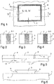
- Figure 1 is a top view of a surface 12 of a layer of negative photoresist 2, which is applied on a bottom layer 1.
- a resist structure 3 that is to be produced from the negative photoresist is indicated in Figure 1 by a rectangular area.
- the area of the resist structure 3 may instead comprise any other shape or pattern according to individual requirements, in particular a triangle, a polygon having more than four corners, a circle or an ellipse.
- the resist structure 3 may comprise a plurality of areas of such shapes, which may be similar or different from one another and may be arranged at equal or different distances from one another.
- the resist structure 3 may especially be intended as a lift-off mask, which will be used to structure a layer that is deposited on the lift-off mask.
- the bottom layer 1 may be a semiconductor substrate or wafer, for instance, or a layer that is arranged on or above a substrate.
- the resist structure 3 that is to be produced from the negative photoresist is surrounded by a border zone 4 within the layer of negative photoresist 2.
- a width 14 of the border zone 4 is indicated in Figure 1 by arrows.
- the border zone 4 is provided with a pattern 5 comprising a dimension that is smaller than a minimal resolution of the irradiation that is intended to produce a locally selective insolubility of the negative photoresist.
- the pattern 5 is provided to modify the intensity of the radiation reaching different levels below the surface 12 and hence to modify the vertical profile of the solubility of the negative photoresist within the border zone 4 as compared to the vertical profile of the solubility in the centre of the resist structure 3.
- Figure 2 is a magnified view of the section indicated in Figure 1 by a dash-dotted contour.
- the section according to Figure 2 shows an area of the border zone 4 between adjacent areas of the layer of negative photoresist 2, including an area of the resist structure 3 to be produced.
- the border zone 4 is provided with a pattern 5.
- the pattern 5 is a grid-like pattern 5-1 composed of two pluralities of parallel lines, wherein the lines belonging to one of the pluralities are arranged transverse to the lines belonging to the other plurality.
- the distances between the parallel lines may be typically in the range from 100 nm to 700 nm and may especially be constant, thus forming a grid with constant pitch.
- a typical example for a suitable pitch is 400 nm in both directions.
- Figure 3 is a further magnified view of the section indicated in Figure 1 by a dash-dotted contour, the corresponding areas being designated with the same reference numerals.
- the pattern 5 is a pattern of parallel lines 5-2.
- the distances between the parallel lines may be typically in the range from 100 nm to 700 nm and may especially be constant, thus forming an array with constant pitch.
- a typical example for a suitable pitch is 400 nm.
- Figure 4 is still a further magnified view of the section indicated in Figure 1 by a dash-dotted contour, the corresponding areas being designated with the same reference numerals.
- the pattern 5 is a pattern of contact holes 5-3.
- the holes are not provided for contacts, but they can be shaped and produced in a way that is similar to the formation of small via holes.
- the holes may be arranged in a random distribution, or they may be arranged on a regular pattern at equal intervals.
- Such a regular pattern may typically comprise a pitch in the range from 100 nm to 700 nm, which may especially be constant.
- the diameters of the holes may typically be in the range from 200 nm to 400 nm and may be different or equal.
- Figure 5 is a cross section showing the layer of negative photoresist 2 on the upper surface 11 of the bottom layer 1. The position of this cross section is indicated in Figure 1 by the dash-dotted straight lines.
- Figure 5 shows the region of the resist structure 3 to be produced and the border zone 4, which surrounds the resist structure 3 and is therefore present at both lateral boundaries of the resist structure 3.
- the width 14 of the border zone 4 is again indicated by arrows.
- the layer of negative photoresist 2 is irradiated, in particular illuminated by light that is incident on the upper surface 12.
- the pattern 5 of the border zone 4 is preferably designed like a sub-resolution assist feature (SRAF). Contrary to conventional sub-resolution assist features, the pattern 5 is used in a completely different way for the formation of the resist structure 3, in particular by an illumination with a conventional imaging system like a stepper, for instance.
- the dimensions of the resist structure 3 are larger than the resolution limit of the imaging system.
- the pattern 5 comprises a dimension or a structural feature that is smaller than the resolution limit of the imaging system. Because of the different dimensions, the structure of the pattern 5 is not reproduced in detail, but only the general outline of the resist structure 3 is transferred to the layer of negative photoresist 2.
- the porosity or the voids of the pattern 5 allow a larger radiation dose to reach a certain level below the surface 12 and thus to cross-link and harden the negative photoresist in the border zone 4 down to deeper levels below the surface 12 than in the central region surrounded by the border zone 4. The region where the sidewall of the resist structure 3 will be located is thus modified.
- the radiation intensity in the vertical direction through the layer of negative photoresist 2 is controlled in the border zone 4 by setting the relevant dimensions of the pattern 5 to appropriate values.
- the diameter of the holes and the pitch of their array are relevant parameters that can be adapted.
- the radiation dose should be set to be sufficiently high to secure a full cross-linking of the negative photoresist in the border zone 4 down to the bottom layer 1. If a full cross-linking is thus achieved in the border zone 4, the subsequent developing process will stop exactly at the position where the negative photoresist is thoroughly cross-linked down to the bottom layer 1, independently of the amount of developer employed. Therefore the shape and size of the sidewall undercut can be adapted to the requirements of individual applications by setting the relevant parameters, especially the width 14 of the border zone 4.
- Figure 6 is a cross section according to Figure 5 after the formation of the resist structure 3 with an overhanging sidewall 6.
- Other profiles of the sidewall 6, like the one shown in Figure 8 can also be produced by adapting the width 14 of the border zone 4 and the structure of the pattern 5.
- the upper edge of the resist structure 3 overhangs the upper surface 11 of the bottom layer 1, and the reentrant shape of the sidewall 6 is appropriate for an application of the resist structure 3 as a lift-off mask.
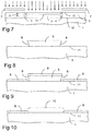
- Figure 7 is a cross section according to Figure 5 showing the irradiation of the layer of negative photoresist 2.
- the layer of negative photoresist 2 is shielded against the radiation by a mask 7 covering the region outside the surface area 13 where the resist structure 3 is to be produced.
- the radiation is indicated in Figure 7 by the arrows pointing down. Below the uncovered surface area 13, the radiation penetrates into the negative photoresist.
- the radiation intensity is a function of the distance D from the surface 12 and decreases with increasing distance D.
- the irradiation is preferably performed in such a way as to render the negative photoresist insoluble in the border zone 4 down to the bottom layer 1.
- Figure 8 is a cross section according to Figure 6 , which shows the produced resist structure 3 after the developing process and after the removal of that portion of the layer of negative photoresist 2 that has not been irradiated.
- the negative slope of the sidewall 6 is essentially at a constant angle with the plane of the surface 11.
- the resist structure 3 according to Figure 8 is also appropriate for an application as a lift-off mask.
- a constant slope of the sidewall 6 can be produced by adopting a suitable pattern 5.
- the diameters of the contact holes can be varied in the direction across the border zone 4, i. e. in the direction following one of the small arrows inserted in Figure 1 , so that the translucency of the pattern 5 comprises a gradient in that direction.
- the pattern 5 comprises a plurality of lines running parallel to the boundary of the border zone 4, the distances between the lines can be varied accordingly.
- Figures 9 and 10 illustrate a lift-off process using the resist structure 3.
- the functional layer 8 is not deposited conformally at the sidewall 6, but is interrupted at the sharp upper edge, thus forming a gap.
- the portion of the functional layer 8 that is applied on the resist structure 3 can therefore easily be removed by removing the resist structure 3, without affecting the remaining portion 9, as shown in Figure 10 .
- the described method uses only negative photoresist, which has an excellent temperature stability, and avoids the disadvantages of producing a double resist layer.
- the shape of the undercut sidewall does not depend as much on the developing process as in conventional photolithographic methods.
- the thorough cross-linking in the region of the sidewall facilitates the control of the undercut and allows narrower design rules than heretofore. Since the attack of the developer is inhibited at the position where the resist is cross-linked down to the bottom layer, the developing process can be performed until the resist is completely removed from the surface area outside the resist structure without affecting the undercut. Furthermore, there is no restriction with respect to a minimal size of the undercut.
- the method is not limited to T-shaped sidewall profiles.
- the areal image intensity can be modified to meet the requirements of a specific application, and vertical reentrant structures can be produced that cannot be realized with conventional methods.
- Feature degradation due to thermal treatment is low, because only cross-linked portions of the photoresist remain after developing, and no stabilizing flood exposure will be necessary.
Landscapes
- Physics & Mathematics (AREA)
- General Physics & Mathematics (AREA)
- Photosensitive Polymer And Photoresist Processing (AREA)
- Exposure And Positioning Against Photoresist Photosensitive Materials (AREA)
Claims (12)
- Procédé de production d'une structure de résist, comprenant:- l'application d'une couche d'un photorésist négatif (2) sur une couche de fond (1),- l'irradiation d'une zone de surface (13) de la couche du photorésist négatif (2) selon la structure de résist (3) à produire, et- l'enlèvement de la couche du photorésist négatif (2) en dehors de la zone de surface (13) irradiée, de manière à former la structure de résist (3),- caractérisé en ce que- la couche du photorésist négatif (2) est pourvue d'un motif (5) formé à l'intérieur de la couche du photorésist négatif (2) dans une zone limitrophe (4) de la structure de résist (3) avant qu'elle ne soit irradiée, le motif (5) comprenant une dimension ou caractéristique de structure qui est plus petite qu'une résolution minimale de l'irradiation.
- Le procédé de la revendication 1, sachant que le motif (5) est prévu comme caractéristique d'assistance subrésolution.
- Le procédé de la revendication 1 ou 2, comprenant en outre:au moins une dimension caractérisant le motif (5), et une largeur (14) de la zone limitrophe (4), la dimension du motif (5) étant plus petite qu'un dizième de la largeur (14) de la zone limitrophe (4).
- Le procédé de l'une des revendications 1 à 3, sachant que le motif (5) comprend une pluralité d'éléments ayant les mêmes dimensions.
- Le procédé de la revendication 4, sachant que les dimensions des éléments sont plus petites qu'un dizième d'une largeur (14) de la zone limitrophe (4).
- Le procédé de la revendication 4 ou 5, sachant que les éléments sont agencés dans un réseau régulier à pas constant.
- Le procédé de la revendication 6, sachant que le pas est plus petit qu'un dizième d'une largeur (14) de la zone limitrophe (4).
- Le procédé de l'une des revendications 1 à 7, sachant que le motif (5) est un motif en grille (5-1).
- Le procédé de l'une des revendications 1 à 7, sachant que le motif (5) est un motif de lignes parallèles (5-2).
- Le procédé de l'une des revendications 1 à 7, sachant que le motif (5) est un motif de trous (5-3).
- Le procédé de l'une des revendications 1 à 10, sachant que la structure de résist (13) est produite avec une paroi latérale (6) décolletée.
- Le procédé de l'une des revendications 1 à 11, sachant que la structure de résist (13) est produite comme masque de décollement.
Priority Applications (5)
| Application Number | Priority Date | Filing Date | Title |
|---|---|---|---|
| EP13179420.8A EP2835687B1 (fr) | 2013-08-06 | 2013-08-06 | Procédé de production d'une structure résistante avec paroi latérale dégagée |
| KR1020167005143A KR101753546B1 (ko) | 2013-08-06 | 2014-07-25 | 언더컷 측벽을 갖는 레지스트 구조를 생산하는 방법 |
| PCT/EP2014/066081 WO2015018672A1 (fr) | 2013-08-06 | 2014-07-25 | Procédé de production d'une structure de masquage dotée d'une paroi latérale avec gravure sous-jacente |
| US14/910,670 US9766546B2 (en) | 2013-08-06 | 2014-07-25 | Method of producing a resist structure with undercut sidewall |
| CN201480044078.1A CN105452957B (zh) | 2013-08-06 | 2014-07-25 | 制作具有底切侧壁的抗蚀剂结构的方法 |
Applications Claiming Priority (1)
| Application Number | Priority Date | Filing Date | Title |
|---|---|---|---|
| EP13179420.8A EP2835687B1 (fr) | 2013-08-06 | 2013-08-06 | Procédé de production d'une structure résistante avec paroi latérale dégagée |
Publications (2)
| Publication Number | Publication Date |
|---|---|
| EP2835687A1 EP2835687A1 (fr) | 2015-02-11 |
| EP2835687B1 true EP2835687B1 (fr) | 2017-03-15 |
Family
ID=48979548
Family Applications (1)
| Application Number | Title | Priority Date | Filing Date |
|---|---|---|---|
| EP13179420.8A Active EP2835687B1 (fr) | 2013-08-06 | 2013-08-06 | Procédé de production d'une structure résistante avec paroi latérale dégagée |
Country Status (5)
| Country | Link |
|---|---|
| US (1) | US9766546B2 (fr) |
| EP (1) | EP2835687B1 (fr) |
| KR (1) | KR101753546B1 (fr) |
| CN (1) | CN105452957B (fr) |
| WO (1) | WO2015018672A1 (fr) |
Families Citing this family (7)
| Publication number | Priority date | Publication date | Assignee | Title |
|---|---|---|---|---|
| CN109952637B (zh) | 2016-12-02 | 2023-10-20 | 英特尔公司 | 用于后段工艺(beol)互连制造的表面对准光刻图案化方式 |
| US12124166B2 (en) | 2017-04-25 | 2024-10-22 | Merck Patent Gmbh | Negative resist formulation for producing undercut pattern profiles |
| CN109164678B (zh) * | 2018-08-15 | 2020-08-28 | 上海华力微电子有限公司 | 改善高深宽比图形不一致和提高光刻胶形貌陡度的方法 |
| TWI717829B (zh) * | 2019-09-10 | 2021-02-01 | 國立交通大學 | 製造iii-v族半導體裝置的互連件之方法,及iii-v族半導體裝置 |
| GB202102706D0 (en) | 2021-02-25 | 2021-04-14 | Ams Ag | Method of manufacturing an optical element |
| DE112022001588T5 (de) | 2021-05-11 | 2024-01-11 | Ams-Osram Ag | Sensorfensteröffnung an einem wellenleiter |
| WO2024208664A1 (fr) | 2023-04-06 | 2024-10-10 | Ams-Osram International Gmbh | Circuit intégré photonique et procédé de fabrication d'un circuit intégré photonique |
Family Cites Families (13)
| Publication number | Priority date | Publication date | Assignee | Title |
|---|---|---|---|---|
| JPS5542376B2 (fr) * | 1971-04-13 | 1980-10-30 | ||
| DE2529054C2 (de) | 1975-06-30 | 1982-04-29 | Ibm Deutschland Gmbh, 7000 Stuttgart | Verfahren zur Herstellung eines zur Vorlage negativen Resistbildes |
| US4024293A (en) | 1975-12-10 | 1977-05-17 | International Business Machines Corporation | High sensitivity resist system for lift-off metallization |
| JPS60135949A (ja) | 1983-12-23 | 1985-07-19 | Matsushita Electric Works Ltd | 光成形体の製造方法 |
| US4564584A (en) | 1983-12-30 | 1986-01-14 | Ibm Corporation | Photoresist lift-off process for fabricating semiconductor devices |
| JPS61156044A (ja) | 1984-12-27 | 1986-07-15 | Nec Corp | レジストステンシルマスクの製造方法 |
| EP0708372B1 (fr) | 1994-10-21 | 2000-03-22 | Ngk Insulators, Ltd. | Procédé de décollage à une seule couche de photoréserve pour former des motifs sur un support |
| JPH08339958A (ja) | 1995-06-13 | 1996-12-24 | Nippon Precision Circuits Kk | レジストパターンの形成方法 |
| US6071652A (en) * | 1997-03-21 | 2000-06-06 | Digital Optics Corporation | Fabricating optical elements using a photoresist formed from contact printing of a gray level mask |
| US6335151B1 (en) * | 1999-06-18 | 2002-01-01 | International Business Machines Corporation | Micro-surface fabrication process |
| US7141338B2 (en) | 2002-11-12 | 2006-11-28 | Infineon Technologies Ag | Sub-resolution sized assist features |
| KR100556044B1 (ko) | 2003-12-31 | 2006-03-03 | 동부아남반도체 주식회사 | 다마신 공정에서의 패턴 향상 방법 |
| US7694269B2 (en) | 2007-02-26 | 2010-04-06 | Texas Instruments Incorporated | Method for positioning sub-resolution assist features |
-
2013
- 2013-08-06 EP EP13179420.8A patent/EP2835687B1/fr active Active
-
2014
- 2014-07-25 KR KR1020167005143A patent/KR101753546B1/ko active Active
- 2014-07-25 US US14/910,670 patent/US9766546B2/en active Active
- 2014-07-25 WO PCT/EP2014/066081 patent/WO2015018672A1/fr not_active Ceased
- 2014-07-25 CN CN201480044078.1A patent/CN105452957B/zh active Active
Non-Patent Citations (1)
| Title |
|---|
| None * |
Also Published As
| Publication number | Publication date |
|---|---|
| CN105452957A (zh) | 2016-03-30 |
| US9766546B2 (en) | 2017-09-19 |
| CN105452957B (zh) | 2019-12-10 |
| KR20160039652A (ko) | 2016-04-11 |
| WO2015018672A1 (fr) | 2015-02-12 |
| US20160179009A1 (en) | 2016-06-23 |
| KR101753546B1 (ko) | 2017-07-03 |
| EP2835687A1 (fr) | 2015-02-11 |
Similar Documents
| Publication | Publication Date | Title |
|---|---|---|
| EP2835687B1 (fr) | Procédé de production d'une structure résistante avec paroi latérale dégagée | |
| US8283111B2 (en) | Method for creating gray-scale features for dual tone development processes | |
| US5532090A (en) | Method and apparatus for enhanced contact and via lithography | |
| JP3385325B2 (ja) | 格子パターンの露光方法および露光装置 | |
| CN107851557B (zh) | 形成用于基板图案化的掩模的方法 | |
| KR101800996B1 (ko) | 기판 상의 콘택 개구 패터닝 방법 | |
| CN101944475B (zh) | 制造半导体器件的方法及图案形成方法 | |
| TWI386764B (zh) | 使用x及y雙極光學元件與單一遮罩的欄柱結構顯像 | |
| CN108292593A (zh) | 使用极紫外光刻对衬底进行图案化的方法 | |
| JP3874989B2 (ja) | パターンの形成方法 | |
| KR100596859B1 (ko) | 반도체 소자의 미세패턴 형성 방법 | |
| KR20100093773A (ko) | 포토 마스크 | |
| KR100948480B1 (ko) | 반도체 소자의 미세 패턴 형성 방법 | |
| KR20010086339A (ko) | 레지스트패턴 제조방법 | |
| EP0825492A1 (fr) | Procédé de traitement d'un motif dans une photoréserve sur une plaquette semi-conductrice | |
| KR100854859B1 (ko) | 반도체 소자의 노광 마스크 및 이를 이용한 감광막 패턴형성 방법 | |
| JP3695430B2 (ja) | 格子パターンの露光方法および露光装置 | |
| TW200300961A (en) | Multiple photolithographic exposures with different clear patterns | |
| KR101023077B1 (ko) | 마스크 패턴 형성 방법 | |
| KR0172587B1 (ko) | 미세 레지스트 패턴 형성방법 | |
| KR20060018722A (ko) | 반도체 장치의 미세 패턴 형성 방법 | |
| TW200423221A (en) | Microlithographic process | |
| KR100742090B1 (ko) | 포토레지스트 패턴의 제조방법 | |
| KR20100059192A (ko) | 반도체 소자의 더블 패터닝 방법 | |
| KR20120098145A (ko) | 반도체 소자의 패턴 형성방법 |
Legal Events
| Date | Code | Title | Description |
|---|---|---|---|
| PUAI | Public reference made under article 153(3) epc to a published international application that has entered the european phase |
Free format text: ORIGINAL CODE: 0009012 |
|
| 17P | Request for examination filed |
Effective date: 20130806 |
|
| AK | Designated contracting states |
Kind code of ref document: A1 Designated state(s): AL AT BE BG CH CY CZ DE DK EE ES FI FR GB GR HR HU IE IS IT LI LT LU LV MC MK MT NL NO PL PT RO RS SE SI SK SM TR |
|
| AX | Request for extension of the european patent |
Extension state: BA ME |
|
| R17P | Request for examination filed (corrected) |
Effective date: 20150513 |
|
| RBV | Designated contracting states (corrected) |
Designated state(s): AL AT BE BG CH CY CZ DE DK EE ES FI FR GB GR HR HU IE IS IT LI LT LU LV MC MK MT NL NO PL PT RO RS SE SI SK SM TR |
|
| REG | Reference to a national code |
Ref country code: DE Ref legal event code: R079 Ref document number: 602013018498 Country of ref document: DE Free format text: PREVIOUS MAIN CLASS: G03F0001540000 Ipc: G03F0007160000 |
|
| GRAP | Despatch of communication of intention to grant a patent |
Free format text: ORIGINAL CODE: EPIDOSNIGR1 |
|
| RIC1 | Information provided on ipc code assigned before grant |
Ipc: G03F 7/16 20060101AFI20160928BHEP |
|
| INTG | Intention to grant announced |
Effective date: 20161020 |
|
| GRAS | Grant fee paid |
Free format text: ORIGINAL CODE: EPIDOSNIGR3 |
|
| GRAA | (expected) grant |
Free format text: ORIGINAL CODE: 0009210 |
|
| AK | Designated contracting states |
Kind code of ref document: B1 Designated state(s): AL AT BE BG CH CY CZ DE DK EE ES FI FR GB GR HR HU IE IS IT LI LT LU LV MC MK MT NL NO PL PT RO RS SE SI SK SM TR |
|
| REG | Reference to a national code |
Ref country code: CH Ref legal event code: EP Ref country code: GB Ref legal event code: FG4D |
|
| REG | Reference to a national code |
Ref country code: IE Ref legal event code: FG4D |
|
| REG | Reference to a national code |
Ref country code: AT Ref legal event code: REF Ref document number: 876170 Country of ref document: AT Kind code of ref document: T Effective date: 20170415 |
|
| REG | Reference to a national code |
Ref country code: DE Ref legal event code: R096 Ref document number: 602013018498 Country of ref document: DE |
|
| REG | Reference to a national code |
Ref country code: NL Ref legal event code: MP Effective date: 20170315 |
|
| REG | Reference to a national code |
Ref country code: LT Ref legal event code: MG4D |
|
| PG25 | Lapsed in a contracting state [announced via postgrant information from national office to epo] |
Ref country code: GR Free format text: LAPSE BECAUSE OF FAILURE TO SUBMIT A TRANSLATION OF THE DESCRIPTION OR TO PAY THE FEE WITHIN THE PRESCRIBED TIME-LIMIT Effective date: 20170616 Ref country code: HR Free format text: LAPSE BECAUSE OF FAILURE TO SUBMIT A TRANSLATION OF THE DESCRIPTION OR TO PAY THE FEE WITHIN THE PRESCRIBED TIME-LIMIT Effective date: 20170315 Ref country code: NO Free format text: LAPSE BECAUSE OF FAILURE TO SUBMIT A TRANSLATION OF THE DESCRIPTION OR TO PAY THE FEE WITHIN THE PRESCRIBED TIME-LIMIT Effective date: 20170615 Ref country code: LT Free format text: LAPSE BECAUSE OF FAILURE TO SUBMIT A TRANSLATION OF THE DESCRIPTION OR TO PAY THE FEE WITHIN THE PRESCRIBED TIME-LIMIT Effective date: 20170315 Ref country code: FI Free format text: LAPSE BECAUSE OF FAILURE TO SUBMIT A TRANSLATION OF THE DESCRIPTION OR TO PAY THE FEE WITHIN THE PRESCRIBED TIME-LIMIT Effective date: 20170315 |
|
| REG | Reference to a national code |
Ref country code: AT Ref legal event code: MK05 Ref document number: 876170 Country of ref document: AT Kind code of ref document: T Effective date: 20170315 |
|
| PG25 | Lapsed in a contracting state [announced via postgrant information from national office to epo] |
Ref country code: LV Free format text: LAPSE BECAUSE OF FAILURE TO SUBMIT A TRANSLATION OF THE DESCRIPTION OR TO PAY THE FEE WITHIN THE PRESCRIBED TIME-LIMIT Effective date: 20170315 Ref country code: BG Free format text: LAPSE BECAUSE OF FAILURE TO SUBMIT A TRANSLATION OF THE DESCRIPTION OR TO PAY THE FEE WITHIN THE PRESCRIBED TIME-LIMIT Effective date: 20170615 Ref country code: RS Free format text: LAPSE BECAUSE OF FAILURE TO SUBMIT A TRANSLATION OF THE DESCRIPTION OR TO PAY THE FEE WITHIN THE PRESCRIBED TIME-LIMIT Effective date: 20170315 Ref country code: SE Free format text: LAPSE BECAUSE OF FAILURE TO SUBMIT A TRANSLATION OF THE DESCRIPTION OR TO PAY THE FEE WITHIN THE PRESCRIBED TIME-LIMIT Effective date: 20170315 |
|
| PG25 | Lapsed in a contracting state [announced via postgrant information from national office to epo] |
Ref country code: NL Free format text: LAPSE BECAUSE OF FAILURE TO SUBMIT A TRANSLATION OF THE DESCRIPTION OR TO PAY THE FEE WITHIN THE PRESCRIBED TIME-LIMIT Effective date: 20170315 |
|
| PG25 | Lapsed in a contracting state [announced via postgrant information from national office to epo] |
Ref country code: CZ Free format text: LAPSE BECAUSE OF FAILURE TO SUBMIT A TRANSLATION OF THE DESCRIPTION OR TO PAY THE FEE WITHIN THE PRESCRIBED TIME-LIMIT Effective date: 20170315 Ref country code: IT Free format text: LAPSE BECAUSE OF FAILURE TO SUBMIT A TRANSLATION OF THE DESCRIPTION OR TO PAY THE FEE WITHIN THE PRESCRIBED TIME-LIMIT Effective date: 20170315 Ref country code: EE Free format text: LAPSE BECAUSE OF FAILURE TO SUBMIT A TRANSLATION OF THE DESCRIPTION OR TO PAY THE FEE WITHIN THE PRESCRIBED TIME-LIMIT Effective date: 20170315 Ref country code: RO Free format text: LAPSE BECAUSE OF FAILURE TO SUBMIT A TRANSLATION OF THE DESCRIPTION OR TO PAY THE FEE WITHIN THE PRESCRIBED TIME-LIMIT Effective date: 20170315 Ref country code: ES Free format text: LAPSE BECAUSE OF FAILURE TO SUBMIT A TRANSLATION OF THE DESCRIPTION OR TO PAY THE FEE WITHIN THE PRESCRIBED TIME-LIMIT Effective date: 20170315 Ref country code: SK Free format text: LAPSE BECAUSE OF FAILURE TO SUBMIT A TRANSLATION OF THE DESCRIPTION OR TO PAY THE FEE WITHIN THE PRESCRIBED TIME-LIMIT Effective date: 20170315 Ref country code: AT Free format text: LAPSE BECAUSE OF FAILURE TO SUBMIT A TRANSLATION OF THE DESCRIPTION OR TO PAY THE FEE WITHIN THE PRESCRIBED TIME-LIMIT Effective date: 20170315 |
|
| PG25 | Lapsed in a contracting state [announced via postgrant information from national office to epo] |
Ref country code: IS Free format text: LAPSE BECAUSE OF FAILURE TO SUBMIT A TRANSLATION OF THE DESCRIPTION OR TO PAY THE FEE WITHIN THE PRESCRIBED TIME-LIMIT Effective date: 20170715 Ref country code: SM Free format text: LAPSE BECAUSE OF FAILURE TO SUBMIT A TRANSLATION OF THE DESCRIPTION OR TO PAY THE FEE WITHIN THE PRESCRIBED TIME-LIMIT Effective date: 20170315 Ref country code: PL Free format text: LAPSE BECAUSE OF FAILURE TO SUBMIT A TRANSLATION OF THE DESCRIPTION OR TO PAY THE FEE WITHIN THE PRESCRIBED TIME-LIMIT Effective date: 20170315 Ref country code: PT Free format text: LAPSE BECAUSE OF FAILURE TO SUBMIT A TRANSLATION OF THE DESCRIPTION OR TO PAY THE FEE WITHIN THE PRESCRIBED TIME-LIMIT Effective date: 20170717 |
|
| REG | Reference to a national code |
Ref country code: DE Ref legal event code: R097 Ref document number: 602013018498 Country of ref document: DE |
|
| PLBE | No opposition filed within time limit |
Free format text: ORIGINAL CODE: 0009261 |
|
| STAA | Information on the status of an ep patent application or granted ep patent |
Free format text: STATUS: NO OPPOSITION FILED WITHIN TIME LIMIT |
|
| PG25 | Lapsed in a contracting state [announced via postgrant information from national office to epo] |
Ref country code: DK Free format text: LAPSE BECAUSE OF FAILURE TO SUBMIT A TRANSLATION OF THE DESCRIPTION OR TO PAY THE FEE WITHIN THE PRESCRIBED TIME-LIMIT Effective date: 20170315 |
|
| 26N | No opposition filed |
Effective date: 20171218 |
|
| PG25 | Lapsed in a contracting state [announced via postgrant information from national office to epo] |
Ref country code: SI Free format text: LAPSE BECAUSE OF FAILURE TO SUBMIT A TRANSLATION OF THE DESCRIPTION OR TO PAY THE FEE WITHIN THE PRESCRIBED TIME-LIMIT Effective date: 20170315 |
|
| REG | Reference to a national code |
Ref country code: CH Ref legal event code: PL |
|
| PG25 | Lapsed in a contracting state [announced via postgrant information from national office to epo] |
Ref country code: MC Free format text: LAPSE BECAUSE OF FAILURE TO SUBMIT A TRANSLATION OF THE DESCRIPTION OR TO PAY THE FEE WITHIN THE PRESCRIBED TIME-LIMIT Effective date: 20170315 |
|
| GBPC | Gb: european patent ceased through non-payment of renewal fee |
Effective date: 20170806 |
|
| PG25 | Lapsed in a contracting state [announced via postgrant information from national office to epo] |
Ref country code: CH Free format text: LAPSE BECAUSE OF NON-PAYMENT OF DUE FEES Effective date: 20170831 Ref country code: LI Free format text: LAPSE BECAUSE OF NON-PAYMENT OF DUE FEES Effective date: 20170831 |
|
| REG | Reference to a national code |
Ref country code: FR Ref legal event code: ST Effective date: 20180430 |
|
| REG | Reference to a national code |
Ref country code: IE Ref legal event code: MM4A |
|
| REG | Reference to a national code |
Ref country code: BE Ref legal event code: MM Effective date: 20170831 |
|
| PG25 | Lapsed in a contracting state [announced via postgrant information from national office to epo] |
Ref country code: LU Free format text: LAPSE BECAUSE OF NON-PAYMENT OF DUE FEES Effective date: 20170806 |
|
| PG25 | Lapsed in a contracting state [announced via postgrant information from national office to epo] |
Ref country code: IE Free format text: LAPSE BECAUSE OF NON-PAYMENT OF DUE FEES Effective date: 20170806 Ref country code: GB Free format text: LAPSE BECAUSE OF NON-PAYMENT OF DUE FEES Effective date: 20170806 |
|
| PG25 | Lapsed in a contracting state [announced via postgrant information from national office to epo] |
Ref country code: BE Free format text: LAPSE BECAUSE OF NON-PAYMENT OF DUE FEES Effective date: 20170831 Ref country code: FR Free format text: LAPSE BECAUSE OF NON-PAYMENT OF DUE FEES Effective date: 20170831 |
|
| PG25 | Lapsed in a contracting state [announced via postgrant information from national office to epo] |
Ref country code: MT Free format text: LAPSE BECAUSE OF NON-PAYMENT OF DUE FEES Effective date: 20170806 |
|
| PG25 | Lapsed in a contracting state [announced via postgrant information from national office to epo] |
Ref country code: HU Free format text: LAPSE BECAUSE OF FAILURE TO SUBMIT A TRANSLATION OF THE DESCRIPTION OR TO PAY THE FEE WITHIN THE PRESCRIBED TIME-LIMIT; INVALID AB INITIO Effective date: 20130806 |
|
| PG25 | Lapsed in a contracting state [announced via postgrant information from national office to epo] |
Ref country code: CY Free format text: LAPSE BECAUSE OF FAILURE TO SUBMIT A TRANSLATION OF THE DESCRIPTION OR TO PAY THE FEE WITHIN THE PRESCRIBED TIME-LIMIT Effective date: 20170315 |
|
| PG25 | Lapsed in a contracting state [announced via postgrant information from national office to epo] |
Ref country code: MK Free format text: LAPSE BECAUSE OF FAILURE TO SUBMIT A TRANSLATION OF THE DESCRIPTION OR TO PAY THE FEE WITHIN THE PRESCRIBED TIME-LIMIT Effective date: 20170315 |
|
| PG25 | Lapsed in a contracting state [announced via postgrant information from national office to epo] |
Ref country code: TR Free format text: LAPSE BECAUSE OF FAILURE TO SUBMIT A TRANSLATION OF THE DESCRIPTION OR TO PAY THE FEE WITHIN THE PRESCRIBED TIME-LIMIT Effective date: 20170315 |
|
| PG25 | Lapsed in a contracting state [announced via postgrant information from national office to epo] |
Ref country code: AL Free format text: LAPSE BECAUSE OF FAILURE TO SUBMIT A TRANSLATION OF THE DESCRIPTION OR TO PAY THE FEE WITHIN THE PRESCRIBED TIME-LIMIT Effective date: 20170315 |
|
| P01 | Opt-out of the competence of the unified patent court (upc) registered |
Effective date: 20230822 |
|
| PGFP | Annual fee paid to national office [announced via postgrant information from national office to epo] |
Ref country code: DE Payment date: 20250820 Year of fee payment: 13 |