EP2838252A1 - Bildsensormodul and und Verfahren zur Herstellung derselben - Google Patents
Bildsensormodul and und Verfahren zur Herstellung derselben Download PDFInfo
- Publication number
- EP2838252A1 EP2838252A1 EP20130191361 EP13191361A EP2838252A1 EP 2838252 A1 EP2838252 A1 EP 2838252A1 EP 20130191361 EP20130191361 EP 20130191361 EP 13191361 A EP13191361 A EP 13191361A EP 2838252 A1 EP2838252 A1 EP 2838252A1
- Authority
- EP
- European Patent Office
- Prior art keywords
- image sensing
- light transmitting
- transmitting element
- disposed
- sensing element
- Prior art date
- Legal status (The legal status is an assumption and is not a legal conclusion. Google has not performed a legal analysis and makes no representation as to the accuracy of the status listed.)
- Granted
Links
Images

Classifications
-
- H—ELECTRICITY
- H10—SEMICONDUCTOR DEVICES; ELECTRIC SOLID-STATE DEVICES NOT OTHERWISE PROVIDED FOR
- H10F—INORGANIC SEMICONDUCTOR DEVICES SENSITIVE TO INFRARED RADIATION, LIGHT, ELECTROMAGNETIC RADIATION OF SHORTER WAVELENGTH OR CORPUSCULAR RADIATION
- H10F55/00—Radiation-sensitive semiconductor devices covered by groups H10F10/00, H10F19/00 or H10F30/00 being structurally associated with electric light sources and electrically or optically coupled thereto
-
- H—ELECTRICITY
- H10—SEMICONDUCTOR DEVICES; ELECTRIC SOLID-STATE DEVICES NOT OTHERWISE PROVIDED FOR
- H10F—INORGANIC SEMICONDUCTOR DEVICES SENSITIVE TO INFRARED RADIATION, LIGHT, ELECTROMAGNETIC RADIATION OF SHORTER WAVELENGTH OR CORPUSCULAR RADIATION
- H10F39/00—Integrated devices, or assemblies of multiple devices, comprising at least one element covered by group H10F30/00, e.g. radiation detectors comprising photodiode arrays
- H10F39/10—Integrated devices
- H10F39/12—Image sensors
-
- H—ELECTRICITY
- H04—ELECTRIC COMMUNICATION TECHNIQUE
- H04N—PICTORIAL COMMUNICATION, e.g. TELEVISION
- H04N23/00—Cameras or camera modules comprising electronic image sensors; Control thereof
- H04N23/50—Constructional details
- H04N23/55—Optical parts specially adapted for electronic image sensors; Mounting thereof
-
- H—ELECTRICITY
- H04—ELECTRIC COMMUNICATION TECHNIQUE
- H04N—PICTORIAL COMMUNICATION, e.g. TELEVISION
- H04N23/00—Cameras or camera modules comprising electronic image sensors; Control thereof
- H04N23/57—Mechanical or electrical details of cameras or camera modules specially adapted for being embedded in other devices
-
- H—ELECTRICITY
- H10—SEMICONDUCTOR DEVICES; ELECTRIC SOLID-STATE DEVICES NOT OTHERWISE PROVIDED FOR
- H10F—INORGANIC SEMICONDUCTOR DEVICES SENSITIVE TO INFRARED RADIATION, LIGHT, ELECTROMAGNETIC RADIATION OF SHORTER WAVELENGTH OR CORPUSCULAR RADIATION
- H10F71/00—Manufacture or treatment of devices covered by this subclass
Definitions
- the instant disclosure relates to an image sensing module and a method of manufacturing the same, and more particularly to an image sensing module for reducing its whole thickness and a method of manufacturing the same.
- CMOS Complementary Metal-Oxide-Semiconductor
- the CMOS image-sensing chip package module can integrate into portable electronic device with small size such as mobile phone and notebook.
- the whole thickness of the image-sensing chip package module of the prior art cannot be reduced.
- One aspect of the instant disclosure relates to an image sensing module for reducing its whole thickness and a method of manufacturing the same.
- an image sensing module comprising: an image sensing unit, a light transmitting unit, a substrate unit and lens unit.
- the image sensing unit includes an image sensing element having an image sensing area on the top side of the image sensing element.
- the light transmitting unit includes a light transmitting element supported above the image sensing element by a plurality of support members, wherein the light transmitting element corresponds to the image sensing area of the image sensing element.
- the substrate unit includes a flexible substrate disposed on the image sensing element and electrically connected to the image sensing element through a plurality of electrical conductors, wherein the flexible substrate has at least one through opening for receiving the light transmitting element, and the at least one through opening corresponds to the image sensing area of the image sensing element.
- the lens unit includes an opaque holder disposed on the flexible substrate to cover the light transmitting element and a lens assembly connected to the opaque holder and disposed above the light transmitting element.
- an image sensing module comprising: an image sensing unit, a light transmitting unit, a substrate unit and lens unit.
- the image sensing unit includes an image sensing element having an image sensing area on the top side of the image sensing element.
- the light transmitting unit includes a light transmitting element supported above the image sensing element by a plurality of support members, wherein the light transmitting element corresponds to the image sensing area of the image sensing element.
- the substrate unit includes a flexible substrate electrically connected to the image sensing element.
- the lens unit includes an opaque holder disposed on the flexible substrate to cover the light transmitting element and a lens assembly connected to the opaque holder and disposed above the light transmitting element, wherein the opaque holder has at least two abutting support legs directly contacting and downwardly abutting against the top surface of the light transmitting element.
- Yet another one of the embodiments of the instant disclosure provides a method of manufacturing an image sensing module, comprising: providing an image sensing element, wherein the image sensing element has an image sensing area on the top side thereof; providing a light transmitting element supported above the image sensing element by a plurality of support members, wherein the light transmitting element corresponds to the image sensing area of the image sensing element; providing a flexible substrate disposed on the image sensing element, wherein the flexible substrate is electrically connected to the image sensing element through a plurality of electrical conductors, the flexible substrate has at least one through opening for receiving the light transmitting element, and the at least one through opening corresponds to the image sensing area of the image sensing element; and then providing a lens unit disposed on the flexible substrate, wherein the lens unit includes an opaque holder disposed on the flexible substrate to cover the light transmitting element and a lens assembly connected to the opaque holder and disposed above the light transmitting element.
- the support members are connected with each other to form a single surrounding support body disposed on the image sensing element to surround the image sensing area, and the light transmitting element is disposed on the single surrounding support body to cover and enclose the image sensing area, wherein the image sensing element is a CMOS image sensor, the light transmitting element is a transparent glass disposed directly above the image sensing area, and the light transmitting element has an infrared coated layer and an antireflection layer respectively formed on the top surface and the bottom surface of the light transmitting element.
- the opaque holder has a surrounding support leg and at least two abutting support legs, the surrounding support leg is disposed on the flexible substrate through adhesive glue, and the at least two abutting support legs directly contact and downwardly abut against the top surface of the light transmitting element.
- the image sensing area of the image sensing element provides a first alignment base level
- the light transmitting element is disposed above the image sensing area of the image sensing element according the first alignment base level
- the light transmitting element provides a second alignment base level on the top surface of the light transmitting element
- the opaque holder is disposed on the top surface of the light transmitting element to directly contact the top surface of the light transmitting element according to the second alignment base level, wherein the image sensing element, the light transmitting element and the opaque holder are sequentially stacked on top of one another.
- the thickness of the light transmitting element can be omitted in the image sensing module of the instant disclosure. Hence, the whole thickness of the image sensing module can be decreased.
- the image sensing element, the light transmitting element and the opaque holder can be sequentially stacked on top of one another according to the design of the first alignment base level provided by the image sensing element and the design of the second alignment base level provided by the light transmitting element.
- the assembly tilt of the opaque holder relative to the image sensing element can be decreased.
- FIG. 1 shows a flowchart of the method of manufacturing an image sensing module for reducing its whole thickness according to the first embodiment of the instant disclosure
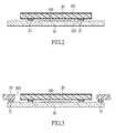
- FIG. 2 shows a schematic view of the method of providing a light transmitting element supported above the image sensing element by a plurality of support members according to the first embodiment of the instant disclosure
- FIG. 3 shows a schematic view of the method of providing a flexible substrate disposed on the image sensing element according to the first embodiment of the instant disclosure
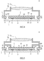
- FIG. 4 shows a schematic view of the image sensing module for reducing its whole thickness according to the first embodiment of the instant disclosure.
- FIG. 5 shows a schematic view of the image sensing module for reducing its whole thickness according to the second embodiment of the instant disclosure.
- the first embodiment of the instant disclosure provides a method of manufacturing an image sensing module M for reducing its whole thickness, comprising the following steps:
- the step S100 is that: referring to FIG. 1 and FIG. 2 , providing an image sensing element 10, wherein the image sensing element 10 has an image sensing area 100 on the top side thereof.
- the image sensing element 10 may be a CMOS (Complementary Metal-Oxide-Semiconductor) image sensor or any image capturing sensor for capturing images.
- CMOS Complementary Metal-Oxide-Semiconductor
- the above-mentioned design for the image sensing element 10 of the first embodiment is merely an example and is not meant to limit the instant disclosure.
- the step S102 is that: referring to FIG. 1 and FIG. 2 , providing a light transmitting element 20 supported above the image sensing element 10 by a plurality of support members 21, wherein the light transmitting element 20 is disposed directly above the image sensing area 100 of the image sensing element 10 for accurately corresponding to the image sensing area 100 of the image sensing element 10. More precisely, the image sensing area 100 of the image sensing element 10 can provide a first alignment base level S1, and the light transmitting element 20 is disposed directly above the image sensing area 100 of the image sensing element 10 according the first alignment base level S1.
- each support member 21 may be an adhesive material or adhesive glue made of epoxy or silicone, and the light transmitting element 20 can be firmly fixed on the image sensing element 10 by curing the support members 21.
- the light transmitting element 20 may be a transparent glass disposed directly above the image sensing area 100, and the light transmitting element 20 has an infrared (IR) coated layer 201 and an antireflection layer 202 respectively formed on the top surface and the bottom surface of the light transmitting element 20.
- IR infrared
- the support members 21 can be connected with each other to form a single surrounding support body disposed on the image sensing element 10 to surround the image sensing area 100, and the light transmitting element 20 is disposed on the single surrounding support body to cover and enclose the image sensing area 100.
- the light transmitting element 20 is disposed on the single surrounding support body to form a cap structure for covering and enclosing the image sensing area 100 of the image sensing element 10, thus the cap structure can be used to prevent the image sensing area 100 from being polluted by external air particles.
- the above-mentioned design for the light transmitting element 20 and the support members 21 of the first embodiment is merely an example and is not meant to limit the instant disclosure.
- the step S104 is that: referring to FIG. 1 and FIG. 3 , providing a flexible substrate 30 disposed on the image sensing element 10, wherein the flexible substrate 30 is electrically connected to the image sensing element 10 through a plurality of electrical conductors 31, the flexible substrate 30 has at least one through opening 300 for receiving the light transmitting element 20, and the at least one through opening 300 is formed directly above the image sensing area 100 of the image sensing element 10 for accurately corresponding to the image sensing area 100 of the image sensing element 10.
- the flexible substrate 10 may be any bendable circuit substrate, but it is merely an example and is not meant to limit the instant disclosure.
- the step S106 is that: referring to FIG. 1 and FIG. 4 , providing a lens unit 4 disposed on the flexible substrate 30, wherein the lens unit 4 includes an opaque holder 40 disposed on the flexible substrate 30 to cover the light transmitting element 20 and a lens assembly 41 connected to the opaque holder 40 and disposed above the light transmitting element 20.
- the lens assembly 41 may be composed of a plurality of lenses, and the lens assembly 41 can be fixedly disposed inside the opaque holder 40 or the lens assembly 41 can be movably disposed inside the opaque holder 40.
- the first embodiment of the instant disclosure provides an image sensing module M for reducing its whole thickness, comprising: an image sensing unit 1, a light transmitting unit 2, a substrate unit 3 and lens unit 4.
- the image sensing unit 1 includes an image sensing element 10 having an image sensing area 100 on the top side of the image sensing element 10.
- the light transmitting unit 2 includes a light transmitting element 20 supported above the image sensing element 10 by a plurality of support members 21 (i.e., the light transmitting element 20 is supported by the support members 21, thus the light transmitting element 20 is positioned above the image sensing element 10).
- the light transmitting element 20 corresponds to the image sensing area 100 of the image sensing element 10, and the light transmitting element 20 has an infrared coated layer 201 and an antireflection layer 202 respectively formed on the top surface and the bottom surface of the light transmitting element 20.
- the substrate unit 3 includes a flexible substrate 30 disposed on the image sensing element 10 through a plurality of electrical conductors 31 (i.e., the flexible substrate 30 is supported by the electrical conductors 31, thus the flexible substrate 30 is positioned above the image sensing element 10), and the flexible substrate 30 is electrically connected to the image sensing element 10 through the electrical conductors 31.
- the flexible substrate 30 has at least one through opening 300 (such as a penetration hole) for receiving the light transmitting element 20, and the at least one through opening 300 corresponds to the image sensing area 100 of the image sensing element 10.
- the lens unit 4 includes an opaque holder 40 disposed on the flexible substrate 30 to cover the light transmitting element 20 and a lens assembly 41 connected to the opaque holder 40 and disposed above the light transmitting element 20.
- the light transmitting element 20 can be disposed on the image sensing element 10 through the support members 21, and the light transmitting element 20 can be received in the at least one through opening 300 of the flexible substrate 30, thus the thickness of the light transmitting element 20 can be omitted in the image sensing module M of the instant disclosure.
- each electrical conductor 31 can be surrounded by adhesive glue (not shown) for firmly positioning the flexible substrate 30 on the image sensing element 10.
- adhesive glue (not shown) for surrounding each electrical conductor 31 can be extended to connect with the single surrounding support body composed of support members 21, in order to prevent the top surface of the image sensing element 10 from being polluted by external air particles passing through the at least one through opening 300.
- the second embodiment of the instant disclosure provides an image sensing module M for reducing its whole thickness, comprising: an image sensing unit 1, a light transmitting unit 2, a substrate unit 3 and lens unit 4.
- the image sensing unit 1 includes an image sensing element 10 having an image sensing area 100 on the top side of the image sensing element 10.
- the light transmitting unit 2 includes a light transmitting element 20 supported above the image sensing element 10 by a plurality of support members 21, and the light transmitting element 20 corresponds to the image sensing area 100 of the image sensing element 10.
- the substrate unit 3 includes a flexible substrate 30 electrically connected to the image sensing element 10.
- the lens unit 4 includes an opaque holder 40 disposed on the flexible substrate 30 to cover the light transmitting element 30 and a lens assembly 41 connected to the opaque holder 40 and disposed above the light transmitting element 20. Furthermore, the opaque holder 40 has a surrounding support leg 400 and at least two abutting support legs 401, the surrounding support leg 400 is disposed on the flexible substrate 30 through adhesive glue 402, and the at least two abutting support legs 401 directly contact and downwardly abut against the top surface of the light transmitting element 20.
- the image sensing area 100 of the image sensing element 10 can provide a first alignment base level S1, and the light transmitting element 20 is disposed directly above the image sensing area 100 of the image sensing element 10 according the first alignment base level S1.
- the light transmitting element 20 can provide a second alignment base level S2 on the top surface of the light transmitting element 20, and the opaque holder 40 is disposed on the top surface of the light transmitting element 20 to directly contact the top surface of the light transmitting element 20 according to the second alignment base level S2.
- the image sensing element 10, the light transmitting element 20 and the opaque holder 40 can be sequentially stacked on top of one another according to the design of the first alignment base level S1 provided by the image sensing element 10 and the design of the second alignment base level S2 provided by the light transmitting element 20, thus the assembly tilt of the opaque holder 40 relative to the image sensing element 10 can be decreased.
- the thickness of the light transmitting element 20 can be omitted in the image sensing module M of the instant disclosure. Hence, the whole thickness of the image sensing module M can be decreased.
- the image sensing element 10 including a light transmitting element 20 supported above the image sensing element 10 by a plurality of support members 21 and the opaque holder 40 having at least two abutting support legs 401 directly contacting and downwardly abutting against the top surface of the light transmitting element 20
- the image sensing element 10, the light transmitting element 20 and the opaque holder 40 can be sequentially stacked on top of one another according to the design of the first alignment base level S1 provided by the image sensing element 10 and the design of the second alignment base level S2 provided by the light transmitting element 20.
- the assembly tilt of the opaque holder 40 relative to the image sensing element 10 can be decreased.
Landscapes
- Engineering & Computer Science (AREA)
- Multimedia (AREA)
- Signal Processing (AREA)
- Transforming Light Signals Into Electric Signals (AREA)
- Studio Devices (AREA)
- Solid State Image Pick-Up Elements (AREA)
- Lens Barrels (AREA)
- Manufacturing & Machinery (AREA)
Applications Claiming Priority (1)
| Application Number | Priority Date | Filing Date | Title |
|---|---|---|---|
| TW102129460A TWI512961B (zh) | 2013-08-16 | 2013-08-16 | 用於降低整體厚度的影像感測模組及其製作方法 |
Publications (2)
| Publication Number | Publication Date |
|---|---|
| EP2838252A1 true EP2838252A1 (de) | 2015-02-18 |
| EP2838252B1 EP2838252B1 (de) | 2022-05-04 |
Family
ID=49585267
Family Applications (1)
| Application Number | Title | Priority Date | Filing Date |
|---|---|---|---|
| EP13191361.8A Active EP2838252B1 (de) | 2013-08-16 | 2013-11-04 | Bildsensormodul and und Verfahren zur Herstellung derselben |
Country Status (6)
| Country | Link |
|---|---|
| US (1) | US9349903B2 (de) |
| EP (1) | EP2838252B1 (de) |
| JP (1) | JP5721285B2 (de) |
| KR (1) | KR101570207B1 (de) |
| CN (1) | CN104377210B (de) |
| TW (1) | TWI512961B (de) |
Families Citing this family (6)
| Publication number | Priority date | Publication date | Assignee | Title |
|---|---|---|---|---|
| US10718922B2 (en) * | 2016-06-01 | 2020-07-21 | Ams Sensors Singapore Pte. Ltd. | Optoelectronic module including lens barrel comprising flanges and adhesive thereon and resting directly on a cover glass |
| TWI639048B (zh) * | 2017-05-22 | 2018-10-21 | 海華科技股份有限公司 | 可攜式電子裝置及其影像擷取模組與承載組件 |
| TWI681424B (zh) * | 2018-06-11 | 2020-01-01 | 海華科技股份有限公司 | 光學元件、光學組件及光學模組 |
| CN110581939B (zh) * | 2019-08-20 | 2021-06-08 | 苏州佳世达电通有限公司 | 摄像装置 |
| KR102901374B1 (ko) * | 2020-01-07 | 2025-12-17 | 엘지이노텍 주식회사 | 카메라 장치 |
| CN115514864B (zh) * | 2021-06-04 | 2024-01-23 | 同欣电子工业股份有限公司 | 无焊接式感测镜头 |
Citations (9)
| Publication number | Priority date | Publication date | Assignee | Title |
|---|---|---|---|---|
| US20040150740A1 (en) * | 2003-01-30 | 2004-08-05 | Hsin Chung Hsien | Miniaturized image sensor module |
| US7084391B1 (en) * | 2005-04-05 | 2006-08-01 | Wen Ching Chen | Image sensing module |
| WO2006093377A1 (en) * | 2005-03-04 | 2006-09-08 | Hyun-Joo Jung | Camera module without focusing adjustment and method of assembling thereof |
| EP1801849A2 (de) * | 2005-12-21 | 2007-06-27 | Sanyo Electric Co. Ltd | Halbleiterbauelement, Verfahren zu seiner Herstellung und Kameramodul |
| US20070212061A1 (en) * | 2006-03-10 | 2007-09-13 | Jae Kun Woo | Camera Module and Method of Manufacturing The same |
| US20080055438A1 (en) * | 2006-08-30 | 2008-03-06 | Samsung Electronics Co., Ltd. | Image sensor package, related method of manufacture and image sensor module |
| US20090040360A1 (en) * | 2006-02-24 | 2009-02-12 | Koji Taniguchi | Imaging device and portable terminal device |
| US20110267535A1 (en) * | 2010-04-29 | 2011-11-03 | Byoung-Rim Seo | Image sensor module having image sensor package |
| US20120141114A1 (en) * | 2010-12-01 | 2012-06-07 | Kwang Jin Gooi | Three-pole tilt control system for camera module |
Family Cites Families (13)
| Publication number | Priority date | Publication date | Assignee | Title |
|---|---|---|---|---|
| JPH0638534Y2 (ja) * | 1987-07-30 | 1994-10-05 | ソニー株式会社 | 撮像装置 |
| JPH11261045A (ja) * | 1998-03-13 | 1999-09-24 | Sony Corp | 撮像素子のパッケージ構造及びそのパッケージ構造を用いた撮像素子の撮像機器への組み付け構造 |
| US6130448A (en) * | 1998-08-21 | 2000-10-10 | Gentex Corporation | Optical sensor package and method of making same |
| JP3821718B2 (ja) * | 2002-01-28 | 2006-09-13 | セイコープレシジョン株式会社 | 固体撮像装置 |
| JP2004309954A (ja) * | 2003-04-10 | 2004-11-04 | Konica Minolta Opto Inc | 撮像装置及びこれを備えた携帯端末 |
| JP4510403B2 (ja) * | 2003-05-08 | 2010-07-21 | 富士フイルム株式会社 | カメラモジュール及びカメラモジュールの製造方法 |
| KR100673950B1 (ko) * | 2004-02-20 | 2007-01-24 | 삼성테크윈 주식회사 | 이미지 센서 모듈과 이를 구비하는 카메라 모듈 패키지 |
| JP2006032886A (ja) * | 2004-06-15 | 2006-02-02 | Fuji Photo Film Co Ltd | 固体撮像装置及びその製造方法及びカメラモジュール |
| TW200739165A (en) * | 2006-04-11 | 2007-10-16 | Chicony Electronic Co Ltd | Lens module of camera and its fabricating method |
| WO2008132802A1 (ja) * | 2007-04-13 | 2008-11-06 | Panasonic Corporation | 固体撮像装置およびその製造方法 |
| US8120128B2 (en) * | 2007-10-12 | 2012-02-21 | Panasonic Corporation | Optical device |
| TW200947638A (en) * | 2008-05-02 | 2009-11-16 | Azurewave Technologies Inc | Image-sensing chip package module with reduced thickness |
| KR101737478B1 (ko) * | 2009-12-14 | 2017-05-19 | 엘지이노텍 주식회사 | 카메라 모듈 및 그 제조 방법 |
-
2013
- 2013-08-16 TW TW102129460A patent/TWI512961B/zh active
- 2013-08-26 CN CN201310376353.7A patent/CN104377210B/zh active Active
- 2013-10-15 JP JP2013214457A patent/JP5721285B2/ja active Active
- 2013-10-17 US US14/055,956 patent/US9349903B2/en active Active
- 2013-11-04 EP EP13191361.8A patent/EP2838252B1/de active Active
- 2013-12-16 KR KR1020130156611A patent/KR101570207B1/ko active Active
Patent Citations (9)
| Publication number | Priority date | Publication date | Assignee | Title |
|---|---|---|---|---|
| US20040150740A1 (en) * | 2003-01-30 | 2004-08-05 | Hsin Chung Hsien | Miniaturized image sensor module |
| WO2006093377A1 (en) * | 2005-03-04 | 2006-09-08 | Hyun-Joo Jung | Camera module without focusing adjustment and method of assembling thereof |
| US7084391B1 (en) * | 2005-04-05 | 2006-08-01 | Wen Ching Chen | Image sensing module |
| EP1801849A2 (de) * | 2005-12-21 | 2007-06-27 | Sanyo Electric Co. Ltd | Halbleiterbauelement, Verfahren zu seiner Herstellung und Kameramodul |
| US20090040360A1 (en) * | 2006-02-24 | 2009-02-12 | Koji Taniguchi | Imaging device and portable terminal device |
| US20070212061A1 (en) * | 2006-03-10 | 2007-09-13 | Jae Kun Woo | Camera Module and Method of Manufacturing The same |
| US20080055438A1 (en) * | 2006-08-30 | 2008-03-06 | Samsung Electronics Co., Ltd. | Image sensor package, related method of manufacture and image sensor module |
| US20110267535A1 (en) * | 2010-04-29 | 2011-11-03 | Byoung-Rim Seo | Image sensor module having image sensor package |
| US20120141114A1 (en) * | 2010-12-01 | 2012-06-07 | Kwang Jin Gooi | Three-pole tilt control system for camera module |
Also Published As
| Publication number | Publication date |
|---|---|
| TWI512961B (zh) | 2015-12-11 |
| US20150048386A1 (en) | 2015-02-19 |
| JP5721285B2 (ja) | 2015-05-20 |
| CN104377210B (zh) | 2017-08-01 |
| KR20150019995A (ko) | 2015-02-25 |
| CN104377210A (zh) | 2015-02-25 |
| EP2838252B1 (de) | 2022-05-04 |
| US9349903B2 (en) | 2016-05-24 |
| JP2015037309A (ja) | 2015-02-23 |
| KR101570207B1 (ko) | 2015-11-20 |
| TW201508903A (zh) | 2015-03-01 |
Similar Documents
| Publication | Publication Date | Title |
|---|---|---|
| US9349903B2 (en) | Image sensing module and method of manufacturing the same | |
| US7632026B2 (en) | Camera module and mobile terminal having the same | |
| US8107005B2 (en) | Method of manufacturing an image sensor module | |
| US20080099864A1 (en) | Chip package, method of making same and digital camera module using the package | |
| EP1814314A2 (de) | Bildaufnahmevorrichtungen, Bildsensormodule und dazugehörige Verfahren | |
| CN108322632A (zh) | 摄像头模组、电子装置及摄像头模组制作方法 | |
| US20190013344A1 (en) | Portable electronic device and image-capturing module thereof, and image-sensing assembly thereof | |
| CN101998034A (zh) | 影像感测模组及相机模组 | |
| US20100025793A1 (en) | Assembly for image sensing chip and assembling method thereof | |
| US20180332202A1 (en) | Portable electronic device and image-capturing module thereof, and carrier assembly thereof | |
| JP2010252164A (ja) | 固体撮像装置 | |
| US20090273698A1 (en) | Image-sensing chip package module for reducing its whole thickness | |
| US11029580B2 (en) | Camera module and optical device | |
| CN205283692U (zh) | 有电磁兼容性屏蔽物(emc)的图像传感器装置 | |
| KR20120007728A (ko) | 카메라 모듈 | |
| US9786709B1 (en) | Portable electronic device and image capturing module thereof | |
| CN111147628B (zh) | 影像撷取组件 | |
| CN113574853B (zh) | 相机模块 | |
| US10658414B1 (en) | Image capturing module and portable electronic device | |
| EP1526579A3 (de) | Festkörperbildsensor und dessen Herstellungsverfahren | |
| KR20000050478A (ko) | 고체 촬상 소자 이미지 센서 모듈 및 그 조립방법 | |
| KR101666599B1 (ko) | 카메라용 이미지센서 패키지 제조방법 | |
| US20130234272A1 (en) | Image-sensing module | |
| US9860431B1 (en) | Portable electronic device and image capturing module thereof | |
| KR102118452B1 (ko) | 카메라 모듈 |
Legal Events
| Date | Code | Title | Description |
|---|---|---|---|
| 17P | Request for examination filed |
Effective date: 20131104 |
|
| AK | Designated contracting states |
Kind code of ref document: A1 Designated state(s): AL AT BE BG CH CY CZ DE DK EE ES FI FR GB GR HR HU IE IS IT LI LT LU LV MC MK MT NL NO PL PT RO RS SE SI SK SM TR |
|
| AX | Request for extension of the european patent |
Extension state: BA ME |
|
| PUAI | Public reference made under article 153(3) epc to a published international application that has entered the european phase |
Free format text: ORIGINAL CODE: 0009012 |
|
| R17P | Request for examination filed (corrected) |
Effective date: 20150409 |
|
| RBV | Designated contracting states (corrected) |
Designated state(s): AL AT BE BG CH CY CZ DE DK EE ES FI FR GB GR HR HU IE IS IT LI LT LU LV MC MK MT NL NO PL PT RO RS SE SI SK SM TR |
|
| STAA | Information on the status of an ep patent application or granted ep patent |
Free format text: STATUS: EXAMINATION IS IN PROGRESS |
|
| 17Q | First examination report despatched |
Effective date: 20161221 |
|
| GRAP | Despatch of communication of intention to grant a patent |
Free format text: ORIGINAL CODE: EPIDOSNIGR1 |
|
| STAA | Information on the status of an ep patent application or granted ep patent |
Free format text: STATUS: GRANT OF PATENT IS INTENDED |
|
| INTG | Intention to grant announced |
Effective date: 20220111 |
|
| GRAS | Grant fee paid |
Free format text: ORIGINAL CODE: EPIDOSNIGR3 |
|
| GRAA | (expected) grant |
Free format text: ORIGINAL CODE: 0009210 |
|
| STAA | Information on the status of an ep patent application or granted ep patent |
Free format text: STATUS: THE PATENT HAS BEEN GRANTED |
|
| AK | Designated contracting states |
Kind code of ref document: B1 Designated state(s): AL AT BE BG CH CY CZ DE DK EE ES FI FR GB GR HR HU IE IS IT LI LT LU LV MC MK MT NL NO PL PT RO RS SE SI SK SM TR |
|
| REG | Reference to a national code |
Ref country code: GB Ref legal event code: FG4D |
|
| REG | Reference to a national code |
Ref country code: CH Ref legal event code: EP |
|
| REG | Reference to a national code |
Ref country code: AT Ref legal event code: REF Ref document number: 1490392 Country of ref document: AT Kind code of ref document: T Effective date: 20220515 |
|
| REG | Reference to a national code |
Ref country code: DE Ref legal event code: R096 Ref document number: 602013081541 Country of ref document: DE |
|
| REG | Reference to a national code |
Ref country code: IE Ref legal event code: FG4D |
|
| REG | Reference to a national code |
Ref country code: LT Ref legal event code: MG9D |
|
| REG | Reference to a national code |
Ref country code: NL Ref legal event code: MP Effective date: 20220504 |
|
| REG | Reference to a national code |
Ref country code: AT Ref legal event code: MK05 Ref document number: 1490392 Country of ref document: AT Kind code of ref document: T Effective date: 20220504 |
|
| PG25 | Lapsed in a contracting state [announced via postgrant information from national office to epo] |
Ref country code: SE Free format text: LAPSE BECAUSE OF FAILURE TO SUBMIT A TRANSLATION OF THE DESCRIPTION OR TO PAY THE FEE WITHIN THE PRESCRIBED TIME-LIMIT Effective date: 20220504 Ref country code: PT Free format text: LAPSE BECAUSE OF FAILURE TO SUBMIT A TRANSLATION OF THE DESCRIPTION OR TO PAY THE FEE WITHIN THE PRESCRIBED TIME-LIMIT Effective date: 20220905 Ref country code: NO Free format text: LAPSE BECAUSE OF FAILURE TO SUBMIT A TRANSLATION OF THE DESCRIPTION OR TO PAY THE FEE WITHIN THE PRESCRIBED TIME-LIMIT Effective date: 20220804 Ref country code: NL Free format text: LAPSE BECAUSE OF FAILURE TO SUBMIT A TRANSLATION OF THE DESCRIPTION OR TO PAY THE FEE WITHIN THE PRESCRIBED TIME-LIMIT Effective date: 20220504 Ref country code: LT Free format text: LAPSE BECAUSE OF FAILURE TO SUBMIT A TRANSLATION OF THE DESCRIPTION OR TO PAY THE FEE WITHIN THE PRESCRIBED TIME-LIMIT Effective date: 20220504 Ref country code: HR Free format text: LAPSE BECAUSE OF FAILURE TO SUBMIT A TRANSLATION OF THE DESCRIPTION OR TO PAY THE FEE WITHIN THE PRESCRIBED TIME-LIMIT Effective date: 20220504 Ref country code: GR Free format text: LAPSE BECAUSE OF FAILURE TO SUBMIT A TRANSLATION OF THE DESCRIPTION OR TO PAY THE FEE WITHIN THE PRESCRIBED TIME-LIMIT Effective date: 20220805 Ref country code: FI Free format text: LAPSE BECAUSE OF FAILURE TO SUBMIT A TRANSLATION OF THE DESCRIPTION OR TO PAY THE FEE WITHIN THE PRESCRIBED TIME-LIMIT Effective date: 20220504 Ref country code: ES Free format text: LAPSE BECAUSE OF FAILURE TO SUBMIT A TRANSLATION OF THE DESCRIPTION OR TO PAY THE FEE WITHIN THE PRESCRIBED TIME-LIMIT Effective date: 20220504 Ref country code: BG Free format text: LAPSE BECAUSE OF FAILURE TO SUBMIT A TRANSLATION OF THE DESCRIPTION OR TO PAY THE FEE WITHIN THE PRESCRIBED TIME-LIMIT Effective date: 20220804 Ref country code: AT Free format text: LAPSE BECAUSE OF FAILURE TO SUBMIT A TRANSLATION OF THE DESCRIPTION OR TO PAY THE FEE WITHIN THE PRESCRIBED TIME-LIMIT Effective date: 20220504 |
|
| REG | Reference to a national code |
Ref country code: DE Ref legal event code: R079 Ref document number: 602013081541 Country of ref document: DE Free format text: PREVIOUS MAIN CLASS: H04N0005225000 Ipc: H04N0023000000 |
|
| PG25 | Lapsed in a contracting state [announced via postgrant information from national office to epo] |
Ref country code: RS Free format text: LAPSE BECAUSE OF FAILURE TO SUBMIT A TRANSLATION OF THE DESCRIPTION OR TO PAY THE FEE WITHIN THE PRESCRIBED TIME-LIMIT Effective date: 20220504 Ref country code: PL Free format text: LAPSE BECAUSE OF FAILURE TO SUBMIT A TRANSLATION OF THE DESCRIPTION OR TO PAY THE FEE WITHIN THE PRESCRIBED TIME-LIMIT Effective date: 20220504 Ref country code: LV Free format text: LAPSE BECAUSE OF FAILURE TO SUBMIT A TRANSLATION OF THE DESCRIPTION OR TO PAY THE FEE WITHIN THE PRESCRIBED TIME-LIMIT Effective date: 20220504 Ref country code: IS Free format text: LAPSE BECAUSE OF FAILURE TO SUBMIT A TRANSLATION OF THE DESCRIPTION OR TO PAY THE FEE WITHIN THE PRESCRIBED TIME-LIMIT Effective date: 20220904 |
|
| PG25 | Lapsed in a contracting state [announced via postgrant information from national office to epo] |
Ref country code: SM Free format text: LAPSE BECAUSE OF FAILURE TO SUBMIT A TRANSLATION OF THE DESCRIPTION OR TO PAY THE FEE WITHIN THE PRESCRIBED TIME-LIMIT Effective date: 20220504 Ref country code: SK Free format text: LAPSE BECAUSE OF FAILURE TO SUBMIT A TRANSLATION OF THE DESCRIPTION OR TO PAY THE FEE WITHIN THE PRESCRIBED TIME-LIMIT Effective date: 20220504 Ref country code: RO Free format text: LAPSE BECAUSE OF FAILURE TO SUBMIT A TRANSLATION OF THE DESCRIPTION OR TO PAY THE FEE WITHIN THE PRESCRIBED TIME-LIMIT Effective date: 20220504 Ref country code: EE Free format text: LAPSE BECAUSE OF FAILURE TO SUBMIT A TRANSLATION OF THE DESCRIPTION OR TO PAY THE FEE WITHIN THE PRESCRIBED TIME-LIMIT Effective date: 20220504 Ref country code: DK Free format text: LAPSE BECAUSE OF FAILURE TO SUBMIT A TRANSLATION OF THE DESCRIPTION OR TO PAY THE FEE WITHIN THE PRESCRIBED TIME-LIMIT Effective date: 20220504 Ref country code: CZ Free format text: LAPSE BECAUSE OF FAILURE TO SUBMIT A TRANSLATION OF THE DESCRIPTION OR TO PAY THE FEE WITHIN THE PRESCRIBED TIME-LIMIT Effective date: 20220504 |
|
| REG | Reference to a national code |
Ref country code: DE Ref legal event code: R097 Ref document number: 602013081541 Country of ref document: DE |
|
| PLBE | No opposition filed within time limit |
Free format text: ORIGINAL CODE: 0009261 |
|
| STAA | Information on the status of an ep patent application or granted ep patent |
Free format text: STATUS: NO OPPOSITION FILED WITHIN TIME LIMIT |
|
| PG25 | Lapsed in a contracting state [announced via postgrant information from national office to epo] |
Ref country code: AL Free format text: LAPSE BECAUSE OF FAILURE TO SUBMIT A TRANSLATION OF THE DESCRIPTION OR TO PAY THE FEE WITHIN THE PRESCRIBED TIME-LIMIT Effective date: 20220504 |
|
| 26N | No opposition filed |
Effective date: 20230207 |
|
| PG25 | Lapsed in a contracting state [announced via postgrant information from national office to epo] |
Ref country code: SI Free format text: LAPSE BECAUSE OF FAILURE TO SUBMIT A TRANSLATION OF THE DESCRIPTION OR TO PAY THE FEE WITHIN THE PRESCRIBED TIME-LIMIT Effective date: 20220504 |
|
| PG25 | Lapsed in a contracting state [announced via postgrant information from national office to epo] |
Ref country code: MC Free format text: LAPSE BECAUSE OF FAILURE TO SUBMIT A TRANSLATION OF THE DESCRIPTION OR TO PAY THE FEE WITHIN THE PRESCRIBED TIME-LIMIT Effective date: 20220504 |
|
| REG | Reference to a national code |
Ref country code: CH Ref legal event code: PL |
|
| REG | Reference to a national code |
Ref country code: BE Ref legal event code: MM Effective date: 20221130 |
|
| PG25 | Lapsed in a contracting state [announced via postgrant information from national office to epo] |
Ref country code: LI Free format text: LAPSE BECAUSE OF NON-PAYMENT OF DUE FEES Effective date: 20221130 Ref country code: CH Free format text: LAPSE BECAUSE OF NON-PAYMENT OF DUE FEES Effective date: 20221130 |
|
| PG25 | Lapsed in a contracting state [announced via postgrant information from national office to epo] |
Ref country code: LU Free format text: LAPSE BECAUSE OF NON-PAYMENT OF DUE FEES Effective date: 20221104 |
|
| PG25 | Lapsed in a contracting state [announced via postgrant information from national office to epo] |
Ref country code: IE Free format text: LAPSE BECAUSE OF NON-PAYMENT OF DUE FEES Effective date: 20221104 |
|
| PG25 | Lapsed in a contracting state [announced via postgrant information from national office to epo] |
Ref country code: BE Free format text: LAPSE BECAUSE OF NON-PAYMENT OF DUE FEES Effective date: 20221130 |
|
| PG25 | Lapsed in a contracting state [announced via postgrant information from national office to epo] |
Ref country code: IT Free format text: LAPSE BECAUSE OF FAILURE TO SUBMIT A TRANSLATION OF THE DESCRIPTION OR TO PAY THE FEE WITHIN THE PRESCRIBED TIME-LIMIT Effective date: 20220504 |
|
| PG25 | Lapsed in a contracting state [announced via postgrant information from national office to epo] |
Ref country code: HU Free format text: LAPSE BECAUSE OF FAILURE TO SUBMIT A TRANSLATION OF THE DESCRIPTION OR TO PAY THE FEE WITHIN THE PRESCRIBED TIME-LIMIT; INVALID AB INITIO Effective date: 20131104 |
|
| PG25 | Lapsed in a contracting state [announced via postgrant information from national office to epo] |
Ref country code: CY Free format text: LAPSE BECAUSE OF FAILURE TO SUBMIT A TRANSLATION OF THE DESCRIPTION OR TO PAY THE FEE WITHIN THE PRESCRIBED TIME-LIMIT Effective date: 20220504 |
|
| PG25 | Lapsed in a contracting state [announced via postgrant information from national office to epo] |
Ref country code: MK Free format text: LAPSE BECAUSE OF FAILURE TO SUBMIT A TRANSLATION OF THE DESCRIPTION OR TO PAY THE FEE WITHIN THE PRESCRIBED TIME-LIMIT Effective date: 20220504 |
|
| PG25 | Lapsed in a contracting state [announced via postgrant information from national office to epo] |
Ref country code: TR Free format text: LAPSE BECAUSE OF FAILURE TO SUBMIT A TRANSLATION OF THE DESCRIPTION OR TO PAY THE FEE WITHIN THE PRESCRIBED TIME-LIMIT Effective date: 20220504 |
|
| PG25 | Lapsed in a contracting state [announced via postgrant information from national office to epo] |
Ref country code: MT Free format text: LAPSE BECAUSE OF FAILURE TO SUBMIT A TRANSLATION OF THE DESCRIPTION OR TO PAY THE FEE WITHIN THE PRESCRIBED TIME-LIMIT Effective date: 20220504 |
|
| PG25 | Lapsed in a contracting state [announced via postgrant information from national office to epo] |
Ref country code: BG Free format text: LAPSE BECAUSE OF FAILURE TO SUBMIT A TRANSLATION OF THE DESCRIPTION OR TO PAY THE FEE WITHIN THE PRESCRIBED TIME-LIMIT Effective date: 20220504 |
|
| PG25 | Lapsed in a contracting state [announced via postgrant information from national office to epo] |
Ref country code: BG Free format text: LAPSE BECAUSE OF FAILURE TO SUBMIT A TRANSLATION OF THE DESCRIPTION OR TO PAY THE FEE WITHIN THE PRESCRIBED TIME-LIMIT Effective date: 20220504 |
|
| PGFP | Annual fee paid to national office [announced via postgrant information from national office to epo] |
Ref country code: DE Payment date: 20251014 Year of fee payment: 13 |
|
| PGFP | Annual fee paid to national office [announced via postgrant information from national office to epo] |
Ref country code: GB Payment date: 20251016 Year of fee payment: 13 |
|
| PGFP | Annual fee paid to national office [announced via postgrant information from national office to epo] |
Ref country code: FR Payment date: 20251023 Year of fee payment: 13 |