EP2846355A1 - Substrat électrique et procédé de fabrication de celui-ci - Google Patents
Substrat électrique et procédé de fabrication de celui-ci Download PDFInfo
- Publication number
- EP2846355A1 EP2846355A1 EP14169730.0A EP14169730A EP2846355A1 EP 2846355 A1 EP2846355 A1 EP 2846355A1 EP 14169730 A EP14169730 A EP 14169730A EP 2846355 A1 EP2846355 A1 EP 2846355A1
- Authority
- EP
- European Patent Office
- Prior art keywords
- insulating layer
- electrical circuit
- conductive layer
- layer
- casing
- Prior art date
- Legal status (The legal status is an assumption and is not a legal conclusion. Google has not performed a legal analysis and makes no representation as to the accuracy of the status listed.)
- Withdrawn
Links
Images



Classifications
-
- H—ELECTRICITY
- H10—SEMICONDUCTOR DEVICES; ELECTRIC SOLID-STATE DEVICES NOT OTHERWISE PROVIDED FOR
- H10H—INORGANIC LIGHT-EMITTING SEMICONDUCTOR DEVICES HAVING POTENTIAL BARRIERS
- H10H20/00—Individual inorganic light-emitting semiconductor devices having potential barriers, e.g. light-emitting diodes [LED]
- H10H20/80—Constructional details
- H10H20/85—Packages
- H10H20/8506—Containers
-
- H—ELECTRICITY
- H10—SEMICONDUCTOR DEVICES; ELECTRIC SOLID-STATE DEVICES NOT OTHERWISE PROVIDED FOR
- H10W—GENERIC PACKAGES, INTERCONNECTIONS, CONNECTORS OR OTHER CONSTRUCTIONAL DETAILS OF DEVICES COVERED BY CLASS H10
- H10W74/00—Encapsulations, e.g. protective coatings
- H10W74/10—Encapsulations, e.g. protective coatings characterised by their shape or disposition
- H10W74/111—Encapsulations, e.g. protective coatings characterised by their shape or disposition the semiconductor body being completely enclosed
- H10W74/114—Encapsulations, e.g. protective coatings characterised by their shape or disposition the semiconductor body being completely enclosed by a substrate and the encapsulations
-
- H—ELECTRICITY
- H10—SEMICONDUCTOR DEVICES; ELECTRIC SOLID-STATE DEVICES NOT OTHERWISE PROVIDED FOR
- H10H—INORGANIC LIGHT-EMITTING SEMICONDUCTOR DEVICES HAVING POTENTIAL BARRIERS
- H10H20/00—Individual inorganic light-emitting semiconductor devices having potential barriers, e.g. light-emitting diodes [LED]
- H10H20/01—Manufacture or treatment
- H10H20/036—Manufacture or treatment of packages
-
- H—ELECTRICITY
- H10—SEMICONDUCTOR DEVICES; ELECTRIC SOLID-STATE DEVICES NOT OTHERWISE PROVIDED FOR
- H10H—INORGANIC LIGHT-EMITTING SEMICONDUCTOR DEVICES HAVING POTENTIAL BARRIERS
- H10H20/00—Individual inorganic light-emitting semiconductor devices having potential barriers, e.g. light-emitting diodes [LED]
- H10H20/80—Constructional details
- H10H20/85—Packages
- H10H20/857—Interconnections, e.g. lead-frames, bond wires or solder balls
-
- H—ELECTRICITY
- H10—SEMICONDUCTOR DEVICES; ELECTRIC SOLID-STATE DEVICES NOT OTHERWISE PROVIDED FOR
- H10W—GENERIC PACKAGES, INTERCONNECTIONS, CONNECTORS OR OTHER CONSTRUCTIONAL DETAILS OF DEVICES COVERED BY CLASS H10
- H10W72/00—Interconnections or connectors in packages
- H10W72/50—Bond wires
- H10W72/531—Shapes of wire connectors
- H10W72/5363—Shapes of wire connectors the connected ends being wedge-shaped
-
- H—ELECTRICITY
- H10—SEMICONDUCTOR DEVICES; ELECTRIC SOLID-STATE DEVICES NOT OTHERWISE PROVIDED FOR
- H10W—GENERIC PACKAGES, INTERCONNECTIONS, CONNECTORS OR OTHER CONSTRUCTIONAL DETAILS OF DEVICES COVERED BY CLASS H10
- H10W72/00—Interconnections or connectors in packages
- H10W72/851—Dispositions of multiple connectors or interconnections
- H10W72/874—On different surfaces
- H10W72/884—Die-attach connectors and bond wires
Definitions
- the invention relates to the field of electrical circuits for packaging electronic components. It also relates to a process for manufacturing such electrical circuits.
- Electrical circuits for packaging electronic components are used for mechanically supporting and electrically connecting electronic components, such as LED (Light Emitting Diode), light sensors, integrated circuits, etc.
- LED Light Emitting Diode
- LED Light Emitting Diode
- integrated circuits etc.
- an electrical circuit which has two main faces, a top face and a bottom face, and comprises a substrate extending essentially parallel to the top and bottom face.
- the substrate has essentially a conductive layer made of electrically conducting material, such as copper, lying on an insulating layer made of dielectric material, such as epoxy glass.
- the insulating layer is located on the side of the top face of the substrate.
- the conductive layer is located on the side of the bottom face. Electrical connection pads are made in the conductive layer. Openings are made in the insulating layer so as to connect a semiconductor component attached on the top face side, to the connection pads, through the openings.
- a purpose of the invention is to improve the packaging and the robustness of such electrical circuits.
- an electrical circuit with the features mentioned above and further having an overmolded casing made of plastic material, at least partially covering the substrate, and wherein a cavity is made in the casing for accommodating a semiconductor component, the cavity being opened on the top face and leaving at least a portion of the electrical connection pads uncovered, for connecting them to the semiconductor component.
- the substrate can be flexible and processed through reel-to-reel operations and overmolding a casing allows designing and forming packaging adapted to the use of the electrical circuit. Consequently, the invention combines the productivity and mass production advantages of reel-to-reel processes with an improved robustness and the possibility to create specific packaging designs.
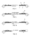
- An insulating layer 1 is supplied from a reel 100 at Fig. 1a .
- This insulating layer 1 consists in a dielectric material such as epoxy glass.
- a glass-reinforced dielectric offers good thermo-mechanical properties and a good dimensional stability.
- This insulating layer 5 is for example about 110 ⁇ m thick.
- a dielectric adhesive or glue layer 3 is coated and/or laminated on one of the main surfaces of the insulating layer 1.
- This adhesive layer 3 is for example about 22 ⁇ m thick.
- This complex comprising the insulating layer 1 and the adhesive layer 3 is then punched at a stamping step ( Fig. 1b ).
- the openings 5 made at this stamping step are drilled though both the insulating layer 1 and the adhesive layer 3.
- an electrically conductive layer 7 is laminated on the adhesive layer 3, and in particular over the openings 5.
- the conductive layer 7 is for example a copper layer about 68 ⁇ m thick.
- This tape is then pattern through a photolithography process in order to design electrical connection pads 9, tracks 11, etc. possibly isolated from each other by gaps 13 etched in the conductive layer 7 ( Fig. 1d ).
- the conductive layer 7 receive, for example by electroplating, a finishing layer 15 on portions (selective coating) or on the whole surface of one or both of its sides ( Fig. 1e ).
- the finishing layer 15 is for example composed of a first layer of nickel 2 ⁇ m thick (directly on the copper) covered by a first silver layer 2 ⁇ m thick on which semiconductor components will be connected.
- a second layer of nickel 1 ⁇ m thick (directly on the copper) is covered by a second silver layer 1 ⁇ m thick. Only the finishing layer 15 on the bottom face is shown on the figures.
- the substrate 20 resulting from these steps is then inserted in a clamping mold 200 ( Fig. 1f ).) At least a portion of the substrate 20 is overmolded: A melted compound, such as a melted plastic material 30 is injected in the mold 200 ( Fig. 1g ) in order to form a casing 40.
- the plastic material 30 is chosen for its high temperature resistance and its UV-resistance.
- the substrate 20 and the casing 40 are ejected from the mold 200 and degated.
- the mold 200 and the casing 40 are represented, but of course one mold 200 can comprise several cavities each one of which corresponding to one casing 40 and /or several molds can be clamped on the substrate 20 at the same time.
- a cavity 41 is made in the casing 40 for accommodating a semiconductor component.
- the cavity 41 is opened on the top face of the substrate 20.
- the cavity leaves at least a portion of the electrical connection pads 9 uncovered for connecting them to the semiconductor component.
- the semiconductor component is a LED, but they can be easily transposed to other kinds of semiconductor component (microchip, die, etc.).
- a LED component 50 is attached and connected, for example with a flip-chip process, to electrical connection pads 9 made in the conductive layer 7.
- electrical connection pads 9 made in the conductive layer 7.
- an eutectic solder is used for this connection.
- the component 50 is then encapsulated (Fig. Ij).
- the encapsulating material 60 is for example a silicone including phosphor for converting blue light to white.
- the encapsulating material 60 is cured ( Fig. 1k ). This curing step can be carried out by batch or through a reel-to-reel process.
- the electrical circuits 70 resulting from the previous steps may be individuated and tested.
- the finishing layer ( Fig. 1e ) can be made selectively with a highly reflective plating on the side (top face) that will receive the LED (in order to enhance the light efficiency in the case of LED packaging).
- the connection pads 9, on this side has a sliver-like reflective surface, for optimizing the reflectance.
- a silver layer is particularly adapted for such an application.
- the finishing layer 15 on the other side (bottom face) may be optimized for improving the efficiency of the soldering or attachment to a heat management system (heat sink).
- the insulating layer 1 and the plastic material 30 are advantageously substantially white for reflecting light.
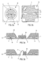
- Figures 2a and 2b respectively show top and bottom faces of an example of electrical circuit 70 obtained at step 1e. (i e. before attachment and connection of a semiconductor component 50).
- the cavity 41 in the casing 40 has substantially a cup shape for reflecting light emitted by the LED (the LED is not shown on Fig. 2a ).
- This electrical circuit 70 has contact pads 9 which are flush with the bottom face ( Fig. 2b ). This can be an advantage for improving the heat dissipation through a heat management system on which the electrical circuit 70 is attached and contacted.
- the electrical circuit 70 comprises one opening 5 through both the conductive layer and the insulating layer 1.
- the plastic material 30 fills this opening 5 and electrically isolates the connection pads 9 from each other.
- the opening 5 in the conductive layer 7 between the connection pads 9 is filled with the plastic material 30 to avoid any leakage when the cup-shape cavity 41 is filled with a liquid product (like a resin, or a silicone, or phosphor containing products).
- the electrical circuit 70 comprises rivets 42 made of plastic material. Indeed, openings 5 through both the conductive layer 7 and the insulating layer 1 are used for injected the plastic material 30.
- the openings 5 being larger in the conductive layer 7 than in the insulating layer 1, a mushroom-shape is obtained which provides kind of plastic rivets 42.
- the head 43 of these plastic rivets 42 is as thick as the conductive layer. This allows to get rid of top surface tensions from the insulating layer 1, and of the peel strength at the interface between the plastic material 30 and the insulating layer 1.
- the reliability of the electrical circuit 70 is increased, in particular with regard to the cohesion through the various layers.
- Another advantage lies in the fact that there is no need for a chemical compatibility in order to have a good mechanical cohesion between the casing 40 and the rest of the structure since rivets 42 provide hooking and mechanical connections.
- the bottom face is maintained flat (for a better heat conduction through a heat management system for example).
- the top face of the conductive layer 7 is flat too for a more reliable connection to the semiconductor component 50.
- Such a structure is suitable for receiving a chip on one side, while the other side may be tailored (with a surface finishing for example) for providing either pads for components, or pads for a connector (e.g. a spring loaded connector, like for smart-cards).
- a connector e.g. a spring loaded connector, like for smart-cards.
- Figs. 3a and 3b also show two different type of connection of the semiconductor component 50 to the pads 9.
- the illustrated connection is a flip-chip connection with solder (eutectic soldering or solder paste) between the semiconductor component 50 and the pads 9.
- solder eutectic soldering or solder paste
- the illustrated connection is a wire bonding connection with wires 51 between pads of the semiconductor component 50 and the connection pads 9 of the electrical circuit 70.
- the electrical circuit 70 obtained by the process discrided above can be used for example for applications in pre-molded Flex Etched Circuits for chip packaging.
- the tape shown on Fig. 4a is similar to the one obtained at Fig. 1d .
- the conductive layer 7 is deformed for example by stamping or roll-to-roll process. Then one or both surfaces of the conductive layer 7 optionally receive finishing layers 15 as explained in relation to Fig. 1e .
- a casing 40 is further overmolded as explained in relation to Figs. 1i to 1l (see fig. 4c ).
- the conductive layer 7 is oriented toward the top face in the cavity 41 and is flush with the bottom face in at least a location corresponding to a connection pad 9.
- the conductive layer 7 is a copper layer about 32 ⁇ m thick.
- a soft copper is advantageously chosen for its ability to deform.
- the insulating layer 1 is made of polyimide and is about 50 ⁇ m thick. Polyimide is chosen for its high dielectric performances.
- the adhesive layer 3 is about 22 ⁇ m thick.
- the nickel layer is about 1 ⁇ m on both sides of the conductive layer 7 and the silver layer is 1.5 ⁇ m thick on the top side of the conductive layer 7 and 3 ⁇ m thick on the bottom side of the conductive layer 7.
- the thickness of the insulating layer 1 is chosen for its ability not to deform during the deformation step of the conductive layer 7.
- the plastic material 30 of the casing 40 is injected on the copper side. This reduces risks of delamination.
- the semiconductor component 50 may be connected to connection pads 9 of the conductive layer 7 by either a wire bonding ( Fig. 4d ) or a flip-chip ( Fig. 4e ) technology.
- Fig. 4d wire bonding
- Fig. 4e flip-chip
- the electrical circuit 70 obtained by the process disclosed in relation to Fig. 4a-4e can be used for example for applications in Quad Flat No Leads - Flex Etched Circuits for chip packaging.
Landscapes
- Wire Bonding (AREA)
Priority Applications (1)
| Application Number | Priority Date | Filing Date | Title |
|---|---|---|---|
| EP14169730.0A EP2846355A1 (fr) | 2013-07-26 | 2014-05-23 | Substrat électrique et procédé de fabrication de celui-ci |
Applications Claiming Priority (2)
| Application Number | Priority Date | Filing Date | Title |
|---|---|---|---|
| EP13178256 | 2013-07-26 | ||
| EP14169730.0A EP2846355A1 (fr) | 2013-07-26 | 2014-05-23 | Substrat électrique et procédé de fabrication de celui-ci |
Publications (1)
| Publication Number | Publication Date |
|---|---|
| EP2846355A1 true EP2846355A1 (fr) | 2015-03-11 |
Family
ID=48906109
Family Applications (1)
| Application Number | Title | Priority Date | Filing Date |
|---|---|---|---|
| EP14169730.0A Withdrawn EP2846355A1 (fr) | 2013-07-26 | 2014-05-23 | Substrat électrique et procédé de fabrication de celui-ci |
Country Status (1)
| Country | Link |
|---|---|
| EP (1) | EP2846355A1 (fr) |
Cited By (2)
| Publication number | Priority date | Publication date | Assignee | Title |
|---|---|---|---|---|
| JP2017069470A (ja) * | 2015-09-30 | 2017-04-06 | 大日本印刷株式会社 | 発光素子用基板、モジュール及び発光素子用基板の製造方法 |
| WO2020012120A1 (fr) | 2018-07-13 | 2020-01-16 | Linxens Holding | Procédé de fabrication de boîtiers de composant électronique et boîtier de composant électronique obtenu par ce procédé |
Citations (5)
| Publication number | Priority date | Publication date | Assignee | Title |
|---|---|---|---|---|
| US20040256466A1 (en) * | 2001-09-18 | 2004-12-23 | Francois Droz | Thin electronic label and method for making same |
| US20080117619A1 (en) * | 2006-11-21 | 2008-05-22 | Siew It Pang | Light source utilizing a flexible circuit carrier and flexible reflectors |
| US20090095969A1 (en) * | 2007-10-11 | 2009-04-16 | Hitachi Chemical Co., Ltd. | Substrate for mounting an optical semiconductor element, manufacturing method thereof, an optical semiconductor device, and manufacturing method thereof |
| US20090224265A1 (en) * | 2008-03-05 | 2009-09-10 | Bily Wang | LED chip package structure with a high-efficiency heat-dissipating substrate and method for making the same |
| WO2012084291A1 (fr) | 2010-12-21 | 2012-06-28 | Microconnections Sas | Procédé de fabrication d'un dispositif monté en surface et dispositif monté en surface correspondant |
-
2014
- 2014-05-23 EP EP14169730.0A patent/EP2846355A1/fr not_active Withdrawn
Patent Citations (5)
| Publication number | Priority date | Publication date | Assignee | Title |
|---|---|---|---|---|
| US20040256466A1 (en) * | 2001-09-18 | 2004-12-23 | Francois Droz | Thin electronic label and method for making same |
| US20080117619A1 (en) * | 2006-11-21 | 2008-05-22 | Siew It Pang | Light source utilizing a flexible circuit carrier and flexible reflectors |
| US20090095969A1 (en) * | 2007-10-11 | 2009-04-16 | Hitachi Chemical Co., Ltd. | Substrate for mounting an optical semiconductor element, manufacturing method thereof, an optical semiconductor device, and manufacturing method thereof |
| US20090224265A1 (en) * | 2008-03-05 | 2009-09-10 | Bily Wang | LED chip package structure with a high-efficiency heat-dissipating substrate and method for making the same |
| WO2012084291A1 (fr) | 2010-12-21 | 2012-06-28 | Microconnections Sas | Procédé de fabrication d'un dispositif monté en surface et dispositif monté en surface correspondant |
Cited By (3)
| Publication number | Priority date | Publication date | Assignee | Title |
|---|---|---|---|---|
| JP2017069470A (ja) * | 2015-09-30 | 2017-04-06 | 大日本印刷株式会社 | 発光素子用基板、モジュール及び発光素子用基板の製造方法 |
| WO2020012120A1 (fr) | 2018-07-13 | 2020-01-16 | Linxens Holding | Procédé de fabrication de boîtiers de composant électronique et boîtier de composant électronique obtenu par ce procédé |
| FR3083920A1 (fr) | 2018-07-13 | 2020-01-17 | Linxens Holding | Procede de fabrication de boitiers de composant electronique et boitier de composant electronique obtenu par ce procede |
Similar Documents
| Publication | Publication Date | Title |
|---|---|---|
| EP2605276B1 (fr) | Dispositif à semi-conducteur sans plomb emballé | |
| US5102829A (en) | Plastic pin grid array package | |
| CN108352355B (zh) | 具有预模制双引线框的半导体系统 | |
| US7679172B2 (en) | Semiconductor package without chip carrier and fabrication method thereof | |
| US6734552B2 (en) | Enhanced thermal dissipation integrated circuit package | |
| KR102400444B1 (ko) | 결합된 도전성 연결 어셈블리를 이용한 패키지된 반도체 장치를 형성하는 방법 및 구조 | |
| JP2006501677A (ja) | ブロック成形集成体用の耐熱強化パッケージ | |
| KR20120002916A (ko) | 엘이디 모듈, 엘이디 패키지와 배선기판 및 그 제조방법 | |
| JP6868455B2 (ja) | 電子部品パッケージおよびその製造方法 | |
| CN101546761A (zh) | 高功率型发光二极管模块封装结构 | |
| JP2012109521A (ja) | Ledモジュール装置及びその製造方法 | |
| CN103219314B (zh) | 电子器件以及用于制造电子器件的方法 | |
| US7825501B2 (en) | High bond line thickness for semiconductor devices | |
| US8697496B1 (en) | Method of manufacture integrated circuit package | |
| EP1627428A1 (fr) | Boitier de circuit integre mettant en application un dissipateur thermique | |
| KR101956119B1 (ko) | 스마트 ic용 인쇄회로기판 및 그 제조방법 | |
| JP2021170679A (ja) | 半導体装置 | |
| CN104347612B (zh) | 集成的无源封装、半导体模块和制造方法 | |
| CN103531695B (zh) | 发光装置用封装成形体及采用了其的发光装置 | |
| CN102395981A (zh) | Ic封装的引线框架和制造方法 | |
| EP4702597A1 (fr) | Structure d'encapsulation de niveau de panneau à interconnexions entièrement parallèles | |
| WO2023048007A1 (fr) | Dispositif électroluminescent et procédé de production d'un dispositif électroluminescent | |
| CN104882386B (zh) | 半导体器件格栅阵列封装 | |
| US20110204386A1 (en) | Metal based electronic component package and the method of manufacturing the same | |
| JP4311294B2 (ja) | 電子装置およびその製造方法 |
Legal Events
| Date | Code | Title | Description |
|---|---|---|---|
| 17P | Request for examination filed |
Effective date: 20140523 |
|
| AK | Designated contracting states |
Kind code of ref document: A1 Designated state(s): AL AT BE BG CH CY CZ DE DK EE ES FI FR GB GR HR HU IE IS IT LI LT LU LV MC MK MT NL NO PL PT RO RS SE SI SK SM TR |
|
| AX | Request for extension of the european patent |
Extension state: BA ME |
|
| PUAI | Public reference made under article 153(3) epc to a published international application that has entered the european phase |
Free format text: ORIGINAL CODE: 0009012 |
|
| R17P | Request for examination filed (corrected) |
Effective date: 20150909 |
|
| RBV | Designated contracting states (corrected) |
Designated state(s): AL AT BE BG CH CY CZ DE DK EE ES FI FR GB GR HR HU IE IS IT LI LT LU LV MC MK MT NL NO PL PT RO RS SE SI SK SM TR |
|
| STAA | Information on the status of an ep patent application or granted ep patent |
Free format text: STATUS: EXAMINATION IS IN PROGRESS |
|
| 17Q | First examination report despatched |
Effective date: 20201016 |
|
| STAA | Information on the status of an ep patent application or granted ep patent |
Free format text: STATUS: THE APPLICATION IS DEEMED TO BE WITHDRAWN |
|
| 18D | Application deemed to be withdrawn |
Effective date: 20210427 |