EP2860669A1 - Verfahren in einem Mikroschaltkreis durgeführt und entsprechende Vorrichtung - Google Patents
Verfahren in einem Mikroschaltkreis durgeführt und entsprechende Vorrichtung Download PDFInfo
- Publication number
- EP2860669A1 EP2860669A1 EP20140188000 EP14188000A EP2860669A1 EP 2860669 A1 EP2860669 A1 EP 2860669A1 EP 20140188000 EP20140188000 EP 20140188000 EP 14188000 A EP14188000 A EP 14188000A EP 2860669 A1 EP2860669 A1 EP 2860669A1
- Authority
- EP
- European Patent Office
- Prior art keywords
- microcircuit
- datum
- normal operation
- address
- identifier
- Prior art date
- Legal status (The legal status is an assumption and is not a legal conclusion. Google has not performed a legal analysis and makes no representation as to the accuracy of the status listed.)
- Granted
Links
Images

Classifications
-
- G—PHYSICS
- G06—COMPUTING OR CALCULATING; COUNTING
- G06K—GRAPHICAL DATA READING; PRESENTATION OF DATA; RECORD CARRIERS; HANDLING RECORD CARRIERS
- G06K19/00—Record carriers for use with machines and with at least a part designed to carry digital markings
- G06K19/06—Record carriers for use with machines and with at least a part designed to carry digital markings characterised by the kind of the digital marking, e.g. shape, nature, code
- G06K19/067—Record carriers with conductive marks, printed circuits or semiconductor circuit elements, e.g. credit or identity cards also with resonating or responding marks without active components
- G06K19/07—Record carriers with conductive marks, printed circuits or semiconductor circuit elements, e.g. credit or identity cards also with resonating or responding marks without active components with integrated circuit chips
- G06K19/073—Special arrangements for circuits, e.g. for protecting identification code in memory
- G06K19/07309—Means for preventing undesired reading or writing from or onto record carriers
- G06K19/07363—Means for preventing undesired reading or writing from or onto record carriers by preventing analysis of the circuit, e.g. dynamic or static power analysis or current analysis
-
- G—PHYSICS
- G06—COMPUTING OR CALCULATING; COUNTING
- G06K—GRAPHICAL DATA READING; PRESENTATION OF DATA; RECORD CARRIERS; HANDLING RECORD CARRIERS
- G06K19/00—Record carriers for use with machines and with at least a part designed to carry digital markings
- G06K19/06—Record carriers for use with machines and with at least a part designed to carry digital markings characterised by the kind of the digital marking, e.g. shape, nature, code
- G06K19/067—Record carriers with conductive marks, printed circuits or semiconductor circuit elements, e.g. credit or identity cards also with resonating or responding marks without active components
- G06K19/07—Record carriers with conductive marks, printed circuits or semiconductor circuit elements, e.g. credit or identity cards also with resonating or responding marks without active components with integrated circuit chips
- G06K19/073—Special arrangements for circuits, e.g. for protecting identification code in memory
- G06K19/07309—Means for preventing undesired reading or writing from or onto record carriers
- G06K19/07372—Means for preventing undesired reading or writing from or onto record carriers by detecting tampering with the circuit
Definitions
- the invention relates to a method and a device for protecting a microcircuit. It applies, in particular, to the protection of microcircuits against attacks, including attacks by fault injection.
- fault injection or fault attack
- a major category of attacks to counteract is constituted by attacks called fault injection (or fault attack), consisting of physically disrupting the chip, for example via a laser, to deflect it from its normal operation, and therefore secured.
- the manufacturer may include detectors for abnormal supply conditions (eg glitches ) or even light and the developers can implement countermeasures, for example to check the integrity of the variables handled, or to test the redundancy of the variables. information.
- detectors for abnormal supply conditions eg glitches
- countermeasures for example to check the integrity of the variables handled, or to test the redundancy of the variables. information.
- the microcircuit can trigger the implementation of protection functions, for example having the effect of deleting the data and / or programs stored in the microcircuit, or to prevent any subsequent operation thereof.
- the number of bytes of a trace (often only 1 byte) is generally smaller than the number of bytes written during a write in normal operation (that is to say when no attack is detected).
- the number of bytes written directly influences the consumption, which makes the writing of the trace detectable.
- the attacker can avoid saving this trace, for example by suddenly cutting power to the card when writing the trace is detected.
- the present invention thus aims to overcome at least one of these disadvantages.
- the device comprises modules configured to implement the various steps of the aforementioned method.
- said identifier makes it possible to identify a type of anomaly.
- said address points to a so-called functional memory zone, different from said dedicated memory zone.
- this dedicated area contains data only when a malfunction has been detected, and it is blank otherwise.
- the dedicated zone may be a sub-zone of the functional zone.
- the dedicated memory area and the functional memory area belong to memories of the same type.
- the data written when the operation of the microcircuit is abnormal comprises at least one byte identical to the data that would be written in the event of normal operation.
- the substituted byte or bytes are located in the header of the data item. This simplifies the extraction of the identifier, without necessarily requiring reading of the entire data.
- the method comprises, following the step of writing in the safe zone, a step of erasing said data from the dedicated memory area.
- Such a condition consists for example in accounting for a certain number of malfunctions of the microcircuit (by counting for example the number of identifiers present in the safe zone).
- the condition may also depend on the nature of the anomaly (i.e. the identifier itself).
- the protection function is a decommissioning function of the microcircuit.
- the microcircuit is therefore not likely to be further damaged by injecting faults from an attacker.
- the data and programs stored in the microcircuit are also protected since the attacker can no longer recover them.
- the step of consulting the dedicated memory area or the step of consulting the secure zone are implemented at the start of the microcircuit, periodically, or when a predefined event is detected.
- such an event may be that an operation counter reaches a predetermined threshold.
- the step of verifying the normal operation of the circuit comprises a step of measuring at least one parameter of the following list: temperature, supply voltage, mismatch ( glitches ), light , clock frequency.
- the data written during the writing makes it possible to keep a record of this parameter.
- the identifier included in the written data can make it possible to precisely identify the parameter whose measurement reveals an anomaly.
- the step of verifying the normal operation of the circuit comprises a step of comparing the results of two executions, or a step of verifying a relationship between two calculation variables, or a step checking a property of a variable.
- the identifier included in the written data in abnormal operation can identify the nature of the operating error.
- the write address in anomalous operation is different from the other write address in abnormal operation.
- the identifier can be returned to an input / output interface of the microcircuit, when powering up the microcircuit or in response to a command received on the interface.
- the various steps of the aforementioned method are determined by instructions of computer programs.
- the invention also relates to a computer program on an information medium, this program being capable of being implemented by a microprocessor, this program comprising instructions adapted to the implementation of the steps of the method such as than mentioned above.
- This program can use any programming language, and be in the form of source code, object code, or intermediate code between source code and object code, such as in a partially compiled form, or in any other form desirable shape.
- the invention is also directed to a microprocessor-readable information medium, and including instructions of a computer program as mentioned above.
- the information carrier may be any entity or device capable of storing the program.
- the medium may comprise storage means, such as a ROM, for example a microcircuit ROM, or a magnetic recording means, for example a hard disk, or a flash memory.
- the information medium may be a transmissible medium such as an electrical or optical signal, which may be conveyed via an electrical or optical cable, by radio or by other means.
- the program according to the invention may in particular be downloaded to a storage platform of an Internet type network.
- the information carrier may be an integrated circuit in which the program is incorporated, the circuit being adapted to execute or to be used in the execution of the method in question.
- the invention relates to the protection of microcircuits and data stored therein, in particular against fault attacks.
- the microcircuit when an operating anomaly, one of whose possible origins is an attack, is detected, the microcircuit performs a write as it would have done in normal operation, except that the written data includes a identifier of abnormal operation, and the writing is done at a specific address, pointing in a dedicated area of memory (also called trash area).
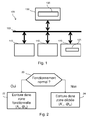
- an identifier whose reading makes it possible to identify an abnormal operation of the microcircuit can be returned to the input / output interface 115, when the microcircuit is powered up or in response to a command received on this interface 115, for example an APDU command.
- a method according to the invention comprises a checking step (20) of the status of operation of the microcircuit.
- this step consists, for example, in measuring an operating parameter of the circuit in order to verify that its value is within a normal range (that is to say characteristic of a normal operation of the microcircuit) of values.
- the verification step may also consist, for example, in checking a checksum or verification (or "checksum” in the English terminology), that is to say, in verifying that data entered in memory are indeed coherent with the checksum associated with these data.
- Some of these steps may possibly be omitted for faster writing.
- step (20) if the verification step (20) reveals a dysfunction of the microcircuit, when the processor commands a writing of a data item A n of n bytes to the address @ A , the latter is modified so as to write (step 24) a data A ' n having the same number n bytes at the address @ A' .
- the modified writing proceeds in exactly the same way as a normal writing whose conventional steps have been described above. Therefore, this modified write has no additional impact on the overall operation of the microcircuit, compared to a normal writing.
- the modification concerns only the nature of the data finally written and the address of the writing.
- the data A ' n is obtained by substituting a number n' of byte (s) of the data item A n by an identifier (or trace) whose reading makes it possible to identify abnormal operation of the microcircuit.
- the data A n may consist of 5 bytes
- the data A ' n may consist of a first byte reflecting for example a temperature anomaly and the last 4 bytes of the data A n .
- the data A n and A ' n are very close in terms of content and are the same size.
- the curve a is the consumption of a normal writing
- the curve b is the consumption of a modified writing (the arrow indicates the moment of the malfunction)
- their signatures in terms of consumption will therefore be very similar, see identical, and an attacker will hardly manage to detect the fact that the writing has been modified.
- the writing of the data A ' n also makes it possible to keep track of the operating anomaly, thanks to the identifier that it includes, preferably in the header in order to facilitate the recognition of the anomaly when a subsequent reading of the data (this case will be described in detail with reference to the Figure 3 ).
- the data A ' n is written to an address @ A' pointing in a specific area of the memory, dedicated to at least temporarily storing the data when an anomaly is detected.
- this dedicated area contains data only when a malfunction of the microcircuit is detected in step 20.
- the identifier whose reading makes it possible to identify an abnormal operation of the microcircuit can be returned to the input / output interface 115 (see FIG. Figure 1 ), when switching on the microcircuit or in response to a command received on this interface 115, for example an APDU command.
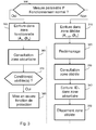
- the Figure 3 represents the steps of a method according to a particular embodiment of the invention. These steps can be implemented by a device according to the invention, for example in the microcircuit 105 of the Figure 1 .
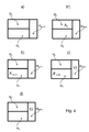
- FIG. 4 representing the state of a memory of the microcircuit (for example the non-volatile memory 130 comprising a memory matrix 135), at different stages of the process.
- the functional writes target different areas of the same memory, namely a conventional write area called functional area M A , a dedicated area M A ' to the data storage in case of malfunction of the microcircuit, and a so-called area safe M SECU where are generally listed traces of anomaly in the state of the art.
- a parameter P of the microcircuit is measured (step 300).
- the memory is empty ( Figure 4a ), that is, the areas M A , M A ' and M SECU are empty.
- a write 305 (similar to step 22 of FIG. Figure 2 ) of the data A n at the address @ A (pointing in the functional area M A ) is executed normally.
- the functional area M A therefore contains the data A n and the dedicated areas M A' and safe M SECU are always empty.
- step 310 the writing is modified (step 310 similar to step 24 of FIG. Figure 2 ) so that a data A ' n, ID comprising an identifier ID of the abnormal operation, for example identifying the parameter P testifying to this abnormal operation, and having the same number n bytes as the data written in normal time A n , written in the dedicated area M A ' at address @ A' .
- the modified writing proceeds in exactly the same way as a normal writing whose conventional steps have been described previously.
- the dedicated area M A ' comprises the data A' n, ID , the areas M A and M SECU remaining empty.
- the microcircuit restarts (step 320).
- This restart can be caused by a user by cutting and then restoring the power of the microcircuit card for example.
- the microcircuit can be restarted periodically or under certain conditions.
- the data A' n, ID is read and during a step 340, the identifier ID that it contains is written in the memory area safe M SECU .
- the identifier is constituted by the byte (s) in the header of the data, reading is facilitated since it is simply read the first byte or bytes of the data.
- the number of bytes (s) to be read may for example be predetermined.
- the dedicated memory area M A ' always includes the data A' n, ID and the safe area M SECU now includes the identifier ID.
- This consultation step 330 may alternatively be initiated after a predetermined period of time (for example periodically), without restarting the terminal, or on detection of a particular event, for example the value of a counter having reached a predetermined threshold. .
- the contents of the dedicated memory M A' are erased during a step 350.
- the Figure 4d represents the state of the memory after this erasure.
- the safe memory zone M SECU is in turn consulted (step 360).
- the safe memory zone M SECU can be consulted at the start of the microcircuit, or when a particular event is detected.
- the safe memory zone M SECU contains the identifier ID of the parameter P.
- test 370 When the content of the safe zone M SECU fulfills certain conditions (test 370), for example when it contains a given number of identifiers, or when it comprises a specific identifier, for example an identifier of the parameter P, then a protection function is implemented.
- such a condition can be of the type 'if the supply voltage is abnormal, then the protection function is implemented' or 'if at least three parameters are faulty, then the protection function is implemented' .
- this protection function can be a decommissioning function of the microcircuit (eg Killcard function).
- a protection function consists in setting to a predetermined value a Killcard Flag having the effect, when read by the microprocessor, for example the immediate destruction of the data contained in the microcircuit, and / or the blocking of the operation thereof.
- step 370 If these conditions are not met in step 370, then the protection function is not performed.
- the operation of the circuit is checked only once.
- the invention covers modes in which several checks are made, and several steps of writing are performed.
- the writes in abnormal operation always target the dedicated area, for example located inside a single page of memory.
- the writes of the corresponding traces are made at different addresses of the dedicated zone, so as not to substitute a trace by another.
- it makes it possible to keep a record of all the anomalies detected before the consultation of the dedicated zone.
- the identifier whose reading makes it possible to identify an abnormal operation of the microcircuit can be returned to the input / output interface 115 (see FIG. Figure 1 ), when switching on the microcircuit or in response to a command received on this interface 115, for example an APDU command.
Landscapes
- Engineering & Computer Science (AREA)
- Computer Hardware Design (AREA)
- Computer Security & Cryptography (AREA)
- General Engineering & Computer Science (AREA)
- Microelectronics & Electronic Packaging (AREA)
- Physics & Mathematics (AREA)
- General Physics & Mathematics (AREA)
- Theoretical Computer Science (AREA)
- Storage Device Security (AREA)
Applications Claiming Priority (1)
| Application Number | Priority Date | Filing Date | Title |
|---|---|---|---|
| FR1359806A FR3011658B1 (fr) | 2013-10-09 | 2013-10-09 | Procede mis en oeuvre dans un microcircuit et dispositif associe |
Publications (2)
| Publication Number | Publication Date |
|---|---|
| EP2860669A1 true EP2860669A1 (de) | 2015-04-15 |
| EP2860669B1 EP2860669B1 (de) | 2020-11-25 |
Family
ID=50289734
Family Applications (1)
| Application Number | Title | Priority Date | Filing Date |
|---|---|---|---|
| EP14188000.5A Active EP2860669B1 (de) | 2013-10-09 | 2014-10-07 | Verfahren in einem Mikroschaltkreis durgeführt und entsprechende Vorrichtung |
Country Status (2)
| Country | Link |
|---|---|
| EP (1) | EP2860669B1 (de) |
| FR (1) | FR3011658B1 (de) |
Cited By (1)
| Publication number | Priority date | Publication date | Assignee | Title |
|---|---|---|---|---|
| FR3045862A1 (fr) * | 2015-12-17 | 2017-06-23 | Oberthur Technologies | Procede d'ecriture dans une memoire non-volatile, procede de lecture dans une memoire non-volatile et procede mis en œuvre dans une entite electronique |
Citations (2)
| Publication number | Priority date | Publication date | Assignee | Title |
|---|---|---|---|---|
| US7039815B1 (en) * | 1999-10-01 | 2006-05-02 | Giesecke & Devrient Gmbh | Method for protecting a data memory |
| FR2935823A1 (fr) | 2008-09-11 | 2010-03-12 | Oberthur Technologies | Procede et dispositif de protection d'un microcircuit contre les attaques. |
-
2013
- 2013-10-09 FR FR1359806A patent/FR3011658B1/fr active Active
-
2014
- 2014-10-07 EP EP14188000.5A patent/EP2860669B1/de active Active
Patent Citations (3)
| Publication number | Priority date | Publication date | Assignee | Title |
|---|---|---|---|---|
| US7039815B1 (en) * | 1999-10-01 | 2006-05-02 | Giesecke & Devrient Gmbh | Method for protecting a data memory |
| FR2935823A1 (fr) | 2008-09-11 | 2010-03-12 | Oberthur Technologies | Procede et dispositif de protection d'un microcircuit contre les attaques. |
| EP2164031B1 (de) * | 2008-09-11 | 2012-07-25 | Oberthur Technologies | Verfahren und Vorrichtung zum Schutz eines Mikroschaltkreises vor Angriffen |
Cited By (1)
| Publication number | Priority date | Publication date | Assignee | Title |
|---|---|---|---|---|
| FR3045862A1 (fr) * | 2015-12-17 | 2017-06-23 | Oberthur Technologies | Procede d'ecriture dans une memoire non-volatile, procede de lecture dans une memoire non-volatile et procede mis en œuvre dans une entite electronique |
Also Published As
| Publication number | Publication date |
|---|---|
| FR3011658A1 (fr) | 2015-04-10 |
| FR3011658B1 (fr) | 2017-02-10 |
| EP2860669B1 (de) | 2020-11-25 |
Similar Documents
| Publication | Publication Date | Title |
|---|---|---|
| EP2164031B1 (de) | Verfahren und Vorrichtung zum Schutz eines Mikroschaltkreises vor Angriffen | |
| FR2849226A1 (fr) | Procede et dispositif de securisation de l'execution d'un programme informatique. | |
| WO2006045924A1 (fr) | Protection contre les attaques par generation de fautes sur les instructions de saut | |
| FR2944117A1 (fr) | Procedes et dispositifs de gestion d'evenements lies a la securite des systemes informatiques d'aeronefs | |
| WO2012175827A1 (fr) | Procédé de gestion de l'endurance de mémoires non volatiles | |
| FR2888960A1 (fr) | Detection d'une faute par perturbation longue | |
| EP2860669B1 (de) | Verfahren in einem Mikroschaltkreis durgeführt und entsprechende Vorrichtung | |
| CA2575143C (fr) | Procede et dispositif de traitement de donnees | |
| EP3391228B1 (de) | Verfahren zum schreiben in einem nichtflüchtigen speicher einer elektronischen einheit und zugehörige elektronische einheit | |
| EP2860668B1 (de) | Verfahren und Vorrichtung zur Funktionserfüllung durch einen Mikroschaltkreis | |
| EP3042334B1 (de) | Verfahren zur installation einer sicherheitsvorrichtung in abhängigkeit einen vertrauensindex in einer elektronischen vorrichtung mit speicher und vorrichtung zur durchführung des verfahrens | |
| FR3100905A1 (fr) | Système sur puce et procédé garantissant la fraicheur des données stockées dans une mémoire extérieure | |
| FR3011650A1 (fr) | Procede et dispositif de realisation de fonction par un microcircuit | |
| EP2229648B1 (de) | Verfahren zur sicheren datenübertragung | |
| EP1715436A2 (de) | Schutz des Ablaufs eines von einem integrierten Schaltkreis ausgeführten Programms oder von Daten, die in diesem Schaltkreis enthalten sind | |
| FR3011657A1 (fr) | Procede mis en œuvre par un processeur et entite electronique associee | |
| EP2104893A2 (de) | Gesicherte elektronische systeme, sicherungsverfahren und verwendung solcher systeme | |
| EP3422232B1 (de) | Schutzverfahren einer elektronischen vorrichtung, die ein programm gegen angriffe durch fehlerinjektion ausführt | |
| FR3068152B1 (fr) | Procede de protection d'un dispositif electronique executant un programme contre des attaques par injection de faute | |
| EP3203405B1 (de) | Verfahren zur ausführung von objektorientierten anwendungsanweisungen durch einen dolmetscher | |
| FR3080474A1 (fr) | Procede de controle de commandes mis en oeuvre par un dispositif tel qu'une carte a puce, et dispositif. | |
| FR2980600A1 (fr) | Procede et systeme de securisation d'une application logicielle comprenant une instruction conditionnelle basee sur une variable booleenne | |
| FR2973150A1 (fr) | Procede de masquage de passage en fin de vie d'un dispositif electronique et dispositif comportant un module de controle correspondant |
Legal Events
| Date | Code | Title | Description |
|---|---|---|---|
| PUAI | Public reference made under article 153(3) epc to a published international application that has entered the european phase |
Free format text: ORIGINAL CODE: 0009012 |
|
| 17P | Request for examination filed |
Effective date: 20141007 |
|
| AK | Designated contracting states |
Kind code of ref document: A1 Designated state(s): AL AT BE BG CH CY CZ DE DK EE ES FI FR GB GR HR HU IE IS IT LI LT LU LV MC MK MT NL NO PL PT RO RS SE SI SK SM TR |
|
| AX | Request for extension of the european patent |
Extension state: BA ME |
|
| R17P | Request for examination filed (corrected) |
Effective date: 20150917 |
|
| RBV | Designated contracting states (corrected) |
Designated state(s): AL AT BE BG CH CY CZ DE DK EE ES FI FR GB GR HR HU IE IS IT LI LT LU LV MC MK MT NL NO PL PT RO RS SE SI SK SM TR |
|
| RAP1 | Party data changed (applicant data changed or rights of an application transferred) |
Owner name: IDEMIA FRANCE |
|
| GRAP | Despatch of communication of intention to grant a patent |
Free format text: ORIGINAL CODE: EPIDOSNIGR1 |
|
| STAA | Information on the status of an ep patent application or granted ep patent |
Free format text: STATUS: GRANT OF PATENT IS INTENDED |
|
| INTG | Intention to grant announced |
Effective date: 20200514 |
|
| GRAS | Grant fee paid |
Free format text: ORIGINAL CODE: EPIDOSNIGR3 |
|
| GRAA | (expected) grant |
Free format text: ORIGINAL CODE: 0009210 |
|
| STAA | Information on the status of an ep patent application or granted ep patent |
Free format text: STATUS: THE PATENT HAS BEEN GRANTED |
|
| AK | Designated contracting states |
Kind code of ref document: B1 Designated state(s): AL AT BE BG CH CY CZ DE DK EE ES FI FR GB GR HR HU IE IS IT LI LT LU LV MC MK MT NL NO PL PT RO RS SE SI SK SM TR |
|
| RAP1 | Party data changed (applicant data changed or rights of an application transferred) |
Owner name: IDEMIA FRANCE |
|
| REG | Reference to a national code |
Ref country code: GB Ref legal event code: FG4D Free format text: NOT ENGLISH |
|
| REG | Reference to a national code |
Ref country code: CH Ref legal event code: EP |
|
| REG | Reference to a national code |
Ref country code: AT Ref legal event code: REF Ref document number: 1339139 Country of ref document: AT Kind code of ref document: T Effective date: 20201215 |
|
| REG | Reference to a national code |
Ref country code: DE Ref legal event code: R096 Ref document number: 602014072637 Country of ref document: DE |
|
| REG | Reference to a national code |
Ref country code: IE Ref legal event code: FG4D Free format text: LANGUAGE OF EP DOCUMENT: FRENCH |
|
| REG | Reference to a national code |
Ref country code: NL Ref legal event code: MP Effective date: 20201125 |
|
| PG25 | Lapsed in a contracting state [announced via postgrant information from national office to epo] |
Ref country code: GR Free format text: LAPSE BECAUSE OF FAILURE TO SUBMIT A TRANSLATION OF THE DESCRIPTION OR TO PAY THE FEE WITHIN THE PRESCRIBED TIME-LIMIT Effective date: 20210226 Ref country code: PT Free format text: LAPSE BECAUSE OF FAILURE TO SUBMIT A TRANSLATION OF THE DESCRIPTION OR TO PAY THE FEE WITHIN THE PRESCRIBED TIME-LIMIT Effective date: 20210325 Ref country code: NO Free format text: LAPSE BECAUSE OF FAILURE TO SUBMIT A TRANSLATION OF THE DESCRIPTION OR TO PAY THE FEE WITHIN THE PRESCRIBED TIME-LIMIT Effective date: 20210225 Ref country code: RS Free format text: LAPSE BECAUSE OF FAILURE TO SUBMIT A TRANSLATION OF THE DESCRIPTION OR TO PAY THE FEE WITHIN THE PRESCRIBED TIME-LIMIT Effective date: 20201125 Ref country code: FI Free format text: LAPSE BECAUSE OF FAILURE TO SUBMIT A TRANSLATION OF THE DESCRIPTION OR TO PAY THE FEE WITHIN THE PRESCRIBED TIME-LIMIT Effective date: 20201125 |
|
| PG25 | Lapsed in a contracting state [announced via postgrant information from national office to epo] |
Ref country code: BG Free format text: LAPSE BECAUSE OF FAILURE TO SUBMIT A TRANSLATION OF THE DESCRIPTION OR TO PAY THE FEE WITHIN THE PRESCRIBED TIME-LIMIT Effective date: 20210225 Ref country code: SE Free format text: LAPSE BECAUSE OF FAILURE TO SUBMIT A TRANSLATION OF THE DESCRIPTION OR TO PAY THE FEE WITHIN THE PRESCRIBED TIME-LIMIT Effective date: 20201125 Ref country code: PL Free format text: LAPSE BECAUSE OF FAILURE TO SUBMIT A TRANSLATION OF THE DESCRIPTION OR TO PAY THE FEE WITHIN THE PRESCRIBED TIME-LIMIT Effective date: 20201125 Ref country code: IS Free format text: LAPSE BECAUSE OF FAILURE TO SUBMIT A TRANSLATION OF THE DESCRIPTION OR TO PAY THE FEE WITHIN THE PRESCRIBED TIME-LIMIT Effective date: 20210325 Ref country code: LV Free format text: LAPSE BECAUSE OF FAILURE TO SUBMIT A TRANSLATION OF THE DESCRIPTION OR TO PAY THE FEE WITHIN THE PRESCRIBED TIME-LIMIT Effective date: 20201125 |
|
| REG | Reference to a national code |
Ref country code: LT Ref legal event code: MG9D |
|
| PG25 | Lapsed in a contracting state [announced via postgrant information from national office to epo] |
Ref country code: HR Free format text: LAPSE BECAUSE OF FAILURE TO SUBMIT A TRANSLATION OF THE DESCRIPTION OR TO PAY THE FEE WITHIN THE PRESCRIBED TIME-LIMIT Effective date: 20201125 |
|
| PG25 | Lapsed in a contracting state [announced via postgrant information from national office to epo] |
Ref country code: CZ Free format text: LAPSE BECAUSE OF FAILURE TO SUBMIT A TRANSLATION OF THE DESCRIPTION OR TO PAY THE FEE WITHIN THE PRESCRIBED TIME-LIMIT Effective date: 20201125 Ref country code: EE Free format text: LAPSE BECAUSE OF FAILURE TO SUBMIT A TRANSLATION OF THE DESCRIPTION OR TO PAY THE FEE WITHIN THE PRESCRIBED TIME-LIMIT Effective date: 20201125 Ref country code: SM Free format text: LAPSE BECAUSE OF FAILURE TO SUBMIT A TRANSLATION OF THE DESCRIPTION OR TO PAY THE FEE WITHIN THE PRESCRIBED TIME-LIMIT Effective date: 20201125 Ref country code: SK Free format text: LAPSE BECAUSE OF FAILURE TO SUBMIT A TRANSLATION OF THE DESCRIPTION OR TO PAY THE FEE WITHIN THE PRESCRIBED TIME-LIMIT Effective date: 20201125 Ref country code: RO Free format text: LAPSE BECAUSE OF FAILURE TO SUBMIT A TRANSLATION OF THE DESCRIPTION OR TO PAY THE FEE WITHIN THE PRESCRIBED TIME-LIMIT Effective date: 20201125 Ref country code: LT Free format text: LAPSE BECAUSE OF FAILURE TO SUBMIT A TRANSLATION OF THE DESCRIPTION OR TO PAY THE FEE WITHIN THE PRESCRIBED TIME-LIMIT Effective date: 20201125 |
|
| REG | Reference to a national code |
Ref country code: DE Ref legal event code: R097 Ref document number: 602014072637 Country of ref document: DE |
|
| PG25 | Lapsed in a contracting state [announced via postgrant information from national office to epo] |
Ref country code: DK Free format text: LAPSE BECAUSE OF FAILURE TO SUBMIT A TRANSLATION OF THE DESCRIPTION OR TO PAY THE FEE WITHIN THE PRESCRIBED TIME-LIMIT Effective date: 20201125 |
|
| REG | Reference to a national code |
Ref country code: AT Ref legal event code: UEP Ref document number: 1339139 Country of ref document: AT Kind code of ref document: T Effective date: 20201125 |
|
| PLBE | No opposition filed within time limit |
Free format text: ORIGINAL CODE: 0009261 |
|
| STAA | Information on the status of an ep patent application or granted ep patent |
Free format text: STATUS: NO OPPOSITION FILED WITHIN TIME LIMIT |
|
| PG25 | Lapsed in a contracting state [announced via postgrant information from national office to epo] |
Ref country code: IT Free format text: LAPSE BECAUSE OF FAILURE TO SUBMIT A TRANSLATION OF THE DESCRIPTION OR TO PAY THE FEE WITHIN THE PRESCRIBED TIME-LIMIT Effective date: 20201125 Ref country code: NL Free format text: LAPSE BECAUSE OF FAILURE TO SUBMIT A TRANSLATION OF THE DESCRIPTION OR TO PAY THE FEE WITHIN THE PRESCRIBED TIME-LIMIT Effective date: 20201125 Ref country code: AL Free format text: LAPSE BECAUSE OF FAILURE TO SUBMIT A TRANSLATION OF THE DESCRIPTION OR TO PAY THE FEE WITHIN THE PRESCRIBED TIME-LIMIT Effective date: 20201125 |
|
| 26N | No opposition filed |
Effective date: 20210826 |
|
| PG25 | Lapsed in a contracting state [announced via postgrant information from national office to epo] |
Ref country code: ES Free format text: LAPSE BECAUSE OF FAILURE TO SUBMIT A TRANSLATION OF THE DESCRIPTION OR TO PAY THE FEE WITHIN THE PRESCRIBED TIME-LIMIT Effective date: 20201125 Ref country code: SI Free format text: LAPSE BECAUSE OF FAILURE TO SUBMIT A TRANSLATION OF THE DESCRIPTION OR TO PAY THE FEE WITHIN THE PRESCRIBED TIME-LIMIT Effective date: 20201125 |
|
| REG | Reference to a national code |
Ref country code: CH Ref legal event code: PL |
|
| PG25 | Lapsed in a contracting state [announced via postgrant information from national office to epo] |
Ref country code: IS Free format text: LAPSE BECAUSE OF FAILURE TO SUBMIT A TRANSLATION OF THE DESCRIPTION OR TO PAY THE FEE WITHIN THE PRESCRIBED TIME-LIMIT Effective date: 20210325 |
|
| REG | Reference to a national code |
Ref country code: BE Ref legal event code: MM Effective date: 20211031 |
|
| GBPC | Gb: european patent ceased through non-payment of renewal fee |
Effective date: 20211007 |
|
| PG25 | Lapsed in a contracting state [announced via postgrant information from national office to epo] |
Ref country code: MC Free format text: LAPSE BECAUSE OF FAILURE TO SUBMIT A TRANSLATION OF THE DESCRIPTION OR TO PAY THE FEE WITHIN THE PRESCRIBED TIME-LIMIT Effective date: 20201125 |
|
| PG25 | Lapsed in a contracting state [announced via postgrant information from national office to epo] |
Ref country code: LU Free format text: LAPSE BECAUSE OF NON-PAYMENT OF DUE FEES Effective date: 20211007 Ref country code: GB Free format text: LAPSE BECAUSE OF NON-PAYMENT OF DUE FEES Effective date: 20211007 Ref country code: BE Free format text: LAPSE BECAUSE OF NON-PAYMENT OF DUE FEES Effective date: 20211031 |
|
| PG25 | Lapsed in a contracting state [announced via postgrant information from national office to epo] |
Ref country code: LI Free format text: LAPSE BECAUSE OF NON-PAYMENT OF DUE FEES Effective date: 20211031 Ref country code: CH Free format text: LAPSE BECAUSE OF NON-PAYMENT OF DUE FEES Effective date: 20211031 |
|
| PG25 | Lapsed in a contracting state [announced via postgrant information from national office to epo] |
Ref country code: IE Free format text: LAPSE BECAUSE OF NON-PAYMENT OF DUE FEES Effective date: 20211007 |
|
| PG25 | Lapsed in a contracting state [announced via postgrant information from national office to epo] |
Ref country code: HU Free format text: LAPSE BECAUSE OF FAILURE TO SUBMIT A TRANSLATION OF THE DESCRIPTION OR TO PAY THE FEE WITHIN THE PRESCRIBED TIME-LIMIT; INVALID AB INITIO Effective date: 20141007 |
|
| P01 | Opt-out of the competence of the unified patent court (upc) registered |
Effective date: 20230428 |
|
| PG25 | Lapsed in a contracting state [announced via postgrant information from national office to epo] |
Ref country code: CY Free format text: LAPSE BECAUSE OF FAILURE TO SUBMIT A TRANSLATION OF THE DESCRIPTION OR TO PAY THE FEE WITHIN THE PRESCRIBED TIME-LIMIT Effective date: 20201125 |
|
| PG25 | Lapsed in a contracting state [announced via postgrant information from national office to epo] |
Ref country code: MK Free format text: LAPSE BECAUSE OF FAILURE TO SUBMIT A TRANSLATION OF THE DESCRIPTION OR TO PAY THE FEE WITHIN THE PRESCRIBED TIME-LIMIT Effective date: 20201125 |
|
| PG25 | Lapsed in a contracting state [announced via postgrant information from national office to epo] |
Ref country code: TR Free format text: LAPSE BECAUSE OF FAILURE TO SUBMIT A TRANSLATION OF THE DESCRIPTION OR TO PAY THE FEE WITHIN THE PRESCRIBED TIME-LIMIT Effective date: 20201125 |
|
| PG25 | Lapsed in a contracting state [announced via postgrant information from national office to epo] |
Ref country code: MT Free format text: LAPSE BECAUSE OF FAILURE TO SUBMIT A TRANSLATION OF THE DESCRIPTION OR TO PAY THE FEE WITHIN THE PRESCRIBED TIME-LIMIT Effective date: 20201125 |
|
| PGFP | Annual fee paid to national office [announced via postgrant information from national office to epo] |
Ref country code: FR Payment date: 20250924 Year of fee payment: 12 |
|
| PGFP | Annual fee paid to national office [announced via postgrant information from national office to epo] |
Ref country code: DE Payment date: 20250923 Year of fee payment: 12 |
|
| PGFP | Annual fee paid to national office [announced via postgrant information from national office to epo] |
Ref country code: AT Payment date: 20250926 Year of fee payment: 12 |