EP2863719A2 - Heizelemente für beheizte Bodenplatten von Flugzeugen - Google Patents
Heizelemente für beheizte Bodenplatten von Flugzeugen Download PDFInfo
- Publication number
- EP2863719A2 EP2863719A2 EP20140188982 EP14188982A EP2863719A2 EP 2863719 A2 EP2863719 A2 EP 2863719A2 EP 20140188982 EP20140188982 EP 20140188982 EP 14188982 A EP14188982 A EP 14188982A EP 2863719 A2 EP2863719 A2 EP 2863719A2
- Authority
- EP
- European Patent Office
- Prior art keywords
- recited
- floor panel
- conductive ink
- temperature
- aircraft
- Prior art date
- Legal status (The legal status is an assumption and is not a legal conclusion. Google has not performed a legal analysis and makes no representation as to the accuracy of the status listed.)
- Granted
Links
Images
Classifications
-
- H—ELECTRICITY
- H05—ELECTRIC TECHNIQUES NOT OTHERWISE PROVIDED FOR
- H05K—PRINTED CIRCUITS; CASINGS OR CONSTRUCTIONAL DETAILS OF ELECTRIC APPARATUS; MANUFACTURE OF ASSEMBLAGES OF ELECTRICAL COMPONENTS
- H05K1/00—Printed circuits
- H05K1/02—Details
- H05K1/0201—Thermal arrangements, e.g. for cooling, heating or preventing overheating
- H05K1/0212—Printed circuits or mounted components having integral heating means
-
- H—ELECTRICITY
- H05—ELECTRIC TECHNIQUES NOT OTHERWISE PROVIDED FOR
- H05B—ELECTRIC HEATING; ELECTRIC LIGHT SOURCES NOT OTHERWISE PROVIDED FOR; CIRCUIT ARRANGEMENTS FOR ELECTRIC LIGHT SOURCES, IN GENERAL
- H05B3/00—Ohmic-resistance heating
- H05B3/20—Heating elements having extended surface area substantially in a two-dimensional [2D] plane, e.g. plate-heater
- H05B3/22—Heating elements having extended surface area substantially in a two-dimensional [2D] plane, e.g. plate-heater non-flexible
- H05B3/26—Heating elements having extended surface area substantially in a two-dimensional [2D] plane, e.g. plate-heater non-flexible heating conductor mounted on insulating base
- H05B3/267—Heating elements having extended surface area substantially in a two-dimensional [2D] plane, e.g. plate-heater non-flexible heating conductor mounted on insulating base the insulating base being an organic material, e.g. plastic
-
- H—ELECTRICITY
- H05—ELECTRIC TECHNIQUES NOT OTHERWISE PROVIDED FOR
- H05K—PRINTED CIRCUITS; CASINGS OR CONSTRUCTIONAL DETAILS OF ELECTRIC APPARATUS; MANUFACTURE OF ASSEMBLAGES OF ELECTRICAL COMPONENTS
- H05K1/00—Printed circuits
- H05K1/02—Details
- H05K1/09—Use of materials for the conductive, e.g. metallic pattern
- H05K1/092—Dispersed materials, e.g. conductive pastes or inks
- H05K1/095—Dispersed materials, e.g. conductive pastes or inks for polymer thick films, i.e. having a permanent organic polymeric binder
-
- H—ELECTRICITY
- H05—ELECTRIC TECHNIQUES NOT OTHERWISE PROVIDED FOR
- H05B—ELECTRIC HEATING; ELECTRIC LIGHT SOURCES NOT OTHERWISE PROVIDED FOR; CIRCUIT ARRANGEMENTS FOR ELECTRIC LIGHT SOURCES, IN GENERAL
- H05B2203/00—Aspects relating to Ohmic resistive heating covered by group H05B3/00
- H05B2203/002—Heaters using a particular layout for the resistive material or resistive elements
- H05B2203/003—Heaters using a particular layout for the resistive material or resistive elements using serpentine layout
-
- H—ELECTRICITY
- H05—ELECTRIC TECHNIQUES NOT OTHERWISE PROVIDED FOR
- H05B—ELECTRIC HEATING; ELECTRIC LIGHT SOURCES NOT OTHERWISE PROVIDED FOR; CIRCUIT ARRANGEMENTS FOR ELECTRIC LIGHT SOURCES, IN GENERAL
- H05B2203/00—Aspects relating to Ohmic resistive heating covered by group H05B3/00
- H05B2203/013—Heaters using resistive films or coatings
-
- H—ELECTRICITY
- H05—ELECTRIC TECHNIQUES NOT OTHERWISE PROVIDED FOR
- H05B—ELECTRIC HEATING; ELECTRIC LIGHT SOURCES NOT OTHERWISE PROVIDED FOR; CIRCUIT ARRANGEMENTS FOR ELECTRIC LIGHT SOURCES, IN GENERAL
- H05B2203/00—Aspects relating to Ohmic resistive heating covered by group H05B3/00
- H05B2203/017—Manufacturing methods or apparatus for heaters
-
- H—ELECTRICITY
- H05—ELECTRIC TECHNIQUES NOT OTHERWISE PROVIDED FOR
- H05K—PRINTED CIRCUITS; CASINGS OR CONSTRUCTIONAL DETAILS OF ELECTRIC APPARATUS; MANUFACTURE OF ASSEMBLAGES OF ELECTRICAL COMPONENTS
- H05K1/00—Printed circuits
- H05K1/02—Details
- H05K1/03—Use of materials for the substrate
- H05K1/0393—Flexible materials
-
- H—ELECTRICITY
- H05—ELECTRIC TECHNIQUES NOT OTHERWISE PROVIDED FOR
- H05K—PRINTED CIRCUITS; CASINGS OR CONSTRUCTIONAL DETAILS OF ELECTRIC APPARATUS; MANUFACTURE OF ASSEMBLAGES OF ELECTRICAL COMPONENTS
- H05K2201/00—Indexing scheme relating to printed circuits covered by H05K1/00
- H05K2201/05—Flexible printed circuits [FPCs]
- H05K2201/056—Folded around rigid support or component
-
- H—ELECTRICITY
- H05—ELECTRIC TECHNIQUES NOT OTHERWISE PROVIDED FOR
- H05K—PRINTED CIRCUITS; CASINGS OR CONSTRUCTIONAL DETAILS OF ELECTRIC APPARATUS; MANUFACTURE OF ASSEMBLAGES OF ELECTRICAL COMPONENTS
- H05K2201/00—Indexing scheme relating to printed circuits covered by H05K1/00
- H05K2201/09—Shape and layout
- H05K2201/09209—Shape and layout details of conductors
- H05K2201/09218—Conductive traces
- H05K2201/09263—Meander
-
- H—ELECTRICITY
- H05—ELECTRIC TECHNIQUES NOT OTHERWISE PROVIDED FOR
- H05K—PRINTED CIRCUITS; CASINGS OR CONSTRUCTIONAL DETAILS OF ELECTRIC APPARATUS; MANUFACTURE OF ASSEMBLAGES OF ELECTRICAL COMPONENTS
- H05K3/00—Apparatus or processes for manufacturing printed circuits
- H05K3/10—Apparatus or processes for manufacturing printed circuits in which conductive material is applied to the insulating support in such a manner as to form the desired conductive pattern
- H05K3/12—Apparatus or processes for manufacturing printed circuits in which conductive material is applied to the insulating support in such a manner as to form the desired conductive pattern using thick film techniques, e.g. printing techniques to apply the conductive material or similar techniques for applying conductive paste or ink patterns
- H05K3/1216—Apparatus or processes for manufacturing printed circuits in which conductive material is applied to the insulating support in such a manner as to form the desired conductive pattern using thick film techniques, e.g. printing techniques to apply the conductive material or similar techniques for applying conductive paste or ink patterns by screen printing or stencil printing
-
- H—ELECTRICITY
- H05—ELECTRIC TECHNIQUES NOT OTHERWISE PROVIDED FOR
- H05K—PRINTED CIRCUITS; CASINGS OR CONSTRUCTIONAL DETAILS OF ELECTRIC APPARATUS; MANUFACTURE OF ASSEMBLAGES OF ELECTRICAL COMPONENTS
- H05K3/00—Apparatus or processes for manufacturing printed circuits
- H05K3/10—Apparatus or processes for manufacturing printed circuits in which conductive material is applied to the insulating support in such a manner as to form the desired conductive pattern
- H05K3/12—Apparatus or processes for manufacturing printed circuits in which conductive material is applied to the insulating support in such a manner as to form the desired conductive pattern using thick film techniques, e.g. printing techniques to apply the conductive material or similar techniques for applying conductive paste or ink patterns
- H05K3/1283—After-treatment of the printed patterns, e.g. sintering or curing methods
Definitions
- the present disclosure relates to heating circuits, and more particularly to resin-based conductive ink circuits.
- resistive heating elements of heated floor panels are chemically etched alloy elements.
- the etch process is fairly involved and requires multiple steps. While satisfactory for its intended purpose the traditional etch process can be time consuming, cause manufacturing difficulties and delay due to over- or under-etch (making resistance too high or too low) or defects due to the photo-print process, and can lead to failure due to mechanical fatigue in the field.
- a method of forming a heating element includes depositing a conductive ink of silver particles in an epoxy resin on a dielectric film to create a conductive circuit, and temperature heat curing the conductive circuit to achieve a resistivity of the heating element less than 1.68 x 10 -6 ohm ⁇ meter.
- the step of heat curing can include curing at a temperature between 155° C - 200° C, and/or at a temperature between a glass transition temperature of the conductive ink and a maximum thermal stability temperature of the conductive ink.
- the glass transition temperature can be lower than the maximum thermal stability temperature and the maximum thermal stability temperature can be greater than 155° C.
- the maximum thermal stability temperature of the conductive ink can exceed 200° C.
- the silver loading can be between 65% - 95% weight/weight of dry ink.
- the silver loading can be between 75% - 89% weight/weight of dry ink.
- the step of depositing can include screen printing the conductive ink onto the dielectric film, and/or can include depositing the conductive ink in a patterned layer.
- the step of curing can include post-curing at a temperature of at least 200° C, and/or can include heat curing at predetermined time intervals.
- the method can also include applying the conductive circuit to at least one panel skin of an aircraft floor panel.
- the conductive ink is configured such that a 0.002 inch (50.8 microns) to .004 inch (101.6 microns) thick post-cure layer of the conductive ink can achieve the resistivity of the heating element and be bent around a 1/4 inch (0.635 cm) diameter cylinder rod without experiencing electric resistance degradation. It is also contemplated that the cylinder rod could have a 1/8 inch (0.3175 cm) diameter, or lower.
- At least one floor panel of an aircraft includes a heating element with a conductive circuit positioned within the floor panel.
- the conductive circuit includes a conductive ink of silver particles in an epoxy resin on a dielectric film.
- the conductive ink can be disposed onto the dielectric film in patterned layers. Further, the silver loading, curing and post-curing temperatures, and resistivity of the heating element can be much as described above.
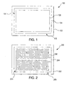
- FIG. 1 an exemplary embodiment of an aircraft heated floor panel in accordance with the disclosure is shown in Fig. 1 and is designated generally by reference character 100.
- FIG. 2 Other embodiments of the aircraft heated floor panel in accordance with the disclosure, or aspects thereof, are provided in Fig. 2 , as will be described.
- the systems and methods described herein can be used heating elements of heated floor panels, and/or other aircraft electrothermal heaters including ice protection systems for high power density, high temperature applications.
- Screen printed resin-based conductive ink heating elements tend to be easier to manufacture than traditional chemically etched alloy resistive heating elements. Screen printed resin-based conductive inks, however, can require low resistivity of the heating elements, for example 1.68 x 10 -6 ohm ⁇ meter or lower. High metal particle loading of the conductive ink can achieve such low resistivity, but there may be a trade-off of reduced mechanical strength.
- an aircraft heated floor panel 100 includes at least one floor panel 102 of an aircraft and a heating element 105 including a conductive circuit 101 positioned within floor panel 102.
- Conductive circuit 101 includes a conductive ink 106 of silver nano-particles in an epoxy resin on a dielectric film 104. While shown schematically as a rectangle, it will be appreciated that conductive ink 106 can be disposed onto dielectric film 104 in a variety of patterned layers, e.g. by screen printing. Multiple screen printed thin layers of conductive ink 106 allow for laterally aligned platelet or needle shape silver particles which tend to cause low electric resistivity.
- the silver loading can be between 65% - 95% weight/weight of dry ink.
- the silver loading can be between 75% - 89% weight/weight of dry ink.
- the conductive circuit 101 can be post-cured at a temperature of 200° C. It may be post-cured at a temperature between a glass transition temperature of the conductive ink and a maximum thermal stability temperature of the conductive ink.
- the resistivity of the heating element 105 may be less than 1.68 x 10 -6 ohm ⁇ meter.
- the maximum thermal stability temperature of the conductive ink can vary as is suitable for a given conductive ink used.
- the glass transition temperature can be lower than the maximum thermal stability temperature and the maximum thermal stability temperature can be greater than 155° C.
- the maximum thermal stability temperature of the conductive ink can exceed 200° C.
- an aircraft heated floor panel 200 includes at least one floor panel 202 of an aircraft and a heating element 205 including a conductive circuit 201 positioned within floor panel 202.
- Conductive circuit 201 includes a conductive ink 206 of silver particles in an epoxy resin on a dielectric film 204, substantially similar to aircraft heated floor panel 100 as described above. In Fig. 2 , however, conductive ink 206 is disposed onto dielectric film 204 in a patterned layer.
- the high silver loading of the conductive ink, post-curing temperatures, and resistivity of heating element, with respect to aircraft heated floor panel 200, can all be similar to those described above with respect to aircraft heated floor panel 100.
- a method of forming a heating element, e.g. heating element 105 or 205, for an aircraft heated floor panel, e.g. aircraft heated floor panel 100 or 200 includes depositing a conductive ink, e.g. conductive ink 106 or 206, of silver particles in an epoxy resin on a dielectric film, e.g. dielectric film 104 or 204, to create a conductive circuit, e.g. conductive circuit 101 or 201.
- the conductive circuit is heat cured at a high temperature to achieve a resistivity of the heating element less than 1.68 x 10 -6 ohm-meter.
- the method of forming the heating element for the aircraft heated floor panel includes applying the conductive circuit to at least one panel skin of an aircraft floor panel, e.g. aircraft floor panel 101 or 202.
- depositing the conductive ink includes depositing a patterned layer of the conductive ink, e.g., as shown in Fig. 2 .
- the step of heat curing can include curing at a temperature between 155° C - 200° C, and/or between a glass transition temperature of the conductive ink and a maximum thermal stability temperature of the conductive ink.
- the step of heat curing can include curing at a temperature greater than 200° C depending on the thermal stability temperature of the conductive ink used.
- the silver loading can be between 65% - 95% weight/weight of dry ink, and/or the step of depositing can include screen printing the conductive ink onto the dielectric film.
- the silver loading can be between 75% - 89% weight/weight of dry ink.
- the step of curing can include post-curing at a temperature of at least 200° C, and/or can include heat curing at predetermined time intervals.
- conductive ink e.g. conductive ink 106
- conductive ink 106 can achieve the resistivity described above without sacrificing mechanical strength and durability.
- a 0.002 inch (50.8 microns) to .004 inch (101.6 microns) thick post-cure layer of conductive ink 106 is configured to be bent around a 1/4 inch (0.635 cm) diameter cylinder rod without experiencing electric resistance degradation.
- cylinder rod can be a 1/8 inch (0.3175 cm) in diameter, or lower.
Landscapes
- Engineering & Computer Science (AREA)
- Microelectronics & Electronic Packaging (AREA)
- Chemical & Material Sciences (AREA)
- Dispersion Chemistry (AREA)
- Surface Heating Bodies (AREA)
- Resistance Heating (AREA)
- Inks, Pencil-Leads, Or Crayons (AREA)
- Manufacturing Of Printed Wiring (AREA)
- Electric Connection Of Electric Components To Printed Circuits (AREA)
- Conductive Materials (AREA)
- Floor Finish (AREA)
- Central Heating Systems (AREA)
Applications Claiming Priority (3)
| Application Number | Priority Date | Filing Date | Title |
|---|---|---|---|
| US201361891276P | 2013-10-15 | 2013-10-15 | |
| US201361891292P | 2013-10-15 | 2013-10-15 | |
| US14/179,281 US9623951B2 (en) | 2013-08-21 | 2014-02-12 | Heating elements for aircraft heated floor panels |
Publications (3)
| Publication Number | Publication Date |
|---|---|
| EP2863719A2 true EP2863719A2 (de) | 2015-04-22 |
| EP2863719A3 EP2863719A3 (de) | 2016-03-09 |
| EP2863719B1 EP2863719B1 (de) | 2020-09-23 |
Family
ID=51730386
Family Applications (2)
| Application Number | Title | Priority Date | Filing Date |
|---|---|---|---|
| EP14188982.4A Active EP2863719B1 (de) | 2013-10-15 | 2014-10-15 | Heizelemente für beheizte Bodenplatten von Flugzeugen |
| EP14189058.2A Active EP2863720B1 (de) | 2013-10-15 | 2014-10-15 | Direktschreibende Sammelschienen für siebgedruckte leitfähige Tinten auf Harzbasis |
Family Applications After (1)
| Application Number | Title | Priority Date | Filing Date |
|---|---|---|---|
| EP14189058.2A Active EP2863720B1 (de) | 2013-10-15 | 2014-10-15 | Direktschreibende Sammelschienen für siebgedruckte leitfähige Tinten auf Harzbasis |
Country Status (2)
| Country | Link |
|---|---|
| EP (2) | EP2863719B1 (de) |
| BR (2) | BR102014025627A2 (de) |
Cited By (1)
| Publication number | Priority date | Publication date | Assignee | Title |
|---|---|---|---|---|
| CN110267370A (zh) * | 2019-06-24 | 2019-09-20 | 东华大学 | 一种保健保暖用柔性电热复合织物及其制备方法与应用 |
Family Cites Families (8)
| Publication number | Priority date | Publication date | Assignee | Title |
|---|---|---|---|---|
| GB2098739B (en) * | 1981-05-16 | 1985-01-16 | Colvern Ltd | Electrical strain gauges |
| JPH01319990A (ja) * | 1988-06-22 | 1989-12-26 | Sumitomo Electric Ind Ltd | 厚膜形成方法 |
| GB2223385B (en) * | 1988-06-22 | 1992-08-26 | Splintex Belge Sa | Vitreous substrate bearing electric circuit components and method of manufacturing same |
| US7304276B2 (en) * | 2001-06-21 | 2007-12-04 | Watlow Electric Manufacturing Company | Thick film heater integrated with low temperature components and method of making the same |
| US7306283B2 (en) * | 2002-11-21 | 2007-12-11 | W.E.T. Automotive Systems Ag | Heater for an automotive vehicle and method of forming same |
| ATE542393T1 (de) * | 2008-03-18 | 2012-02-15 | Watlow Electric Mfg | Geschichtetes heizsystem mit wabenkernstruktur |
| US20100065686A1 (en) * | 2008-04-28 | 2010-03-18 | Tauscher Kurt M | Aircraft heated floor panel |
| DE102011084303A1 (de) * | 2011-10-11 | 2013-04-11 | Continental Automotive Gmbh | Verfahren zur Herstellung eines Trägers für eine leistungselektronische Baugruppe und Träger für eine solche Baugruppe |
-
2014
- 2014-10-14 BR BR102014025627A patent/BR102014025627A2/pt not_active IP Right Cessation
- 2014-10-14 BR BR102014025625-3A patent/BR102014025625A2/pt active Search and Examination
- 2014-10-15 EP EP14188982.4A patent/EP2863719B1/de active Active
- 2014-10-15 EP EP14189058.2A patent/EP2863720B1/de active Active
Non-Patent Citations (1)
| Title |
|---|
| None |
Cited By (1)
| Publication number | Priority date | Publication date | Assignee | Title |
|---|---|---|---|---|
| CN110267370A (zh) * | 2019-06-24 | 2019-09-20 | 东华大学 | 一种保健保暖用柔性电热复合织物及其制备方法与应用 |
Also Published As
| Publication number | Publication date |
|---|---|
| EP2863720B1 (de) | 2025-11-26 |
| BR102014025625A2 (pt) | 2017-12-19 |
| EP2863719B1 (de) | 2020-09-23 |
| EP2863719A3 (de) | 2016-03-09 |
| EP2863720A2 (de) | 2015-04-22 |
| BR102014025627A2 (pt) | 2015-11-10 |
| EP2863720A3 (de) | 2016-03-09 |
Similar Documents
| Publication | Publication Date | Title |
|---|---|---|
| US9623951B2 (en) | Heating elements for aircraft heated floor panels | |
| US20220183114A1 (en) | Multilayered panels | |
| EP2381739B1 (de) | Erwärmungselement und herstellungsverfahren dafür | |
| KR101156275B1 (ko) | 터치스크린 및 이의 제조방법 | |
| EP3419381B1 (de) | Elektrothermische eisschutzsysteme mit kohlenstoffadditivbeladenen thermoplastischen heizelementen | |
| CN102379012B (zh) | 电流检测用金属板电阻器及其制造方法 | |
| JP7300659B2 (ja) | 特注の抵抗を伴う厚膜抵抗器及び製造方法 | |
| SE0950708A1 (sv) | Värmeelement med positiv temperaturkoefficient och deras framställning | |
| CN105050210A (zh) | 加热器及用于制造加热器的方法 | |
| EP2863719B1 (de) | Heizelemente für beheizte Bodenplatten von Flugzeugen | |
| US20190112054A1 (en) | Integrated ice protection and lightning strike prevention | |
| EP3198200B1 (de) | Kochfeld mit sensorelement und verfahren zur herstellung eines kochfeldes | |
| CN201570468U (zh) | 一种电阻式保险丝装置 | |
| JP2007018989A (ja) | 面状発熱体の製造方法およびそれにより製造された面状発熱体 | |
| EP2978285B1 (de) | Verbessertes verfahren zur herstellung gedruckter elektronik | |
| EP3078239B1 (de) | Verbund mit einem exponentiell temperatur- abhängigen elektrischen widerstand, verwendung eines solchen verbund in einem selbstregulierenden heizelment, selbstregulierendes heizelment aufweisend einen solchen verbund und herstellungs- verfahren eines solchen verbund | |
| EP3179827A1 (de) | Flexibles widerstandsheizelement | |
| WO2005055660A2 (de) | Flächenheizelement und verfahren zu seiner herstellung | |
| CN205104313U (zh) | 过电流保护元件 | |
| CN102856028A (zh) | 印刷电阻烘烤定型方法 | |
| Busbaher | Update on development of new generation of cathodes using additive manufacturing methods | |
| CN106033845B (zh) | 超材料及超材料的导电微结构制作方法 | |
| DE2135850A1 (de) | Dehnstoffelement mit elektrischer beheizung |
Legal Events
| Date | Code | Title | Description |
|---|---|---|---|
| PUAI | Public reference made under article 153(3) epc to a published international application that has entered the european phase |
Free format text: ORIGINAL CODE: 0009012 |
|
| 17P | Request for examination filed |
Effective date: 20141015 |
|
| AK | Designated contracting states |
Kind code of ref document: A2 Designated state(s): AL AT BE BG CH CY CZ DE DK EE ES FI FR GB GR HR HU IE IS IT LI LT LU LV MC MK MT NL NO PL PT RO RS SE SI SK SM TR |
|
| AX | Request for extension of the european patent |
Extension state: BA ME |
|
| PUAL | Search report despatched |
Free format text: ORIGINAL CODE: 0009013 |
|
| AK | Designated contracting states |
Kind code of ref document: A3 Designated state(s): AL AT BE BG CH CY CZ DE DK EE ES FI FR GB GR HR HU IE IS IT LI LT LU LV MC MK MT NL NO PL PT RO RS SE SI SK SM TR |
|
| AX | Request for extension of the european patent |
Extension state: BA ME |
|
| RIC1 | Information provided on ipc code assigned before grant |
Ipc: H05B 3/26 20060101ALI20160203BHEP Ipc: H05K 1/02 20060101ALI20160203BHEP Ipc: H05K 3/12 20060101ALI20160203BHEP Ipc: H05K 1/09 20060101AFI20160203BHEP |
|
| R17P | Request for examination filed (corrected) |
Effective date: 20160909 |
|
| RBV | Designated contracting states (corrected) |
Designated state(s): AL AT BE BG CH CY CZ DE DK EE ES FI FR GB GR HR HU IE IS IT LI LT LU LV MC MK MT NL NO PL PT RO RS SE SI SK SM TR |
|
| GRAP | Despatch of communication of intention to grant a patent |
Free format text: ORIGINAL CODE: EPIDOSNIGR1 |
|
| STAA | Information on the status of an ep patent application or granted ep patent |
Free format text: STATUS: GRANT OF PATENT IS INTENDED |
|
| INTG | Intention to grant announced |
Effective date: 20200414 |
|
| GRAS | Grant fee paid |
Free format text: ORIGINAL CODE: EPIDOSNIGR3 |
|
| GRAA | (expected) grant |
Free format text: ORIGINAL CODE: 0009210 |
|
| STAA | Information on the status of an ep patent application or granted ep patent |
Free format text: STATUS: THE PATENT HAS BEEN GRANTED |
|
| AK | Designated contracting states |
Kind code of ref document: B1 Designated state(s): AL AT BE BG CH CY CZ DE DK EE ES FI FR GB GR HR HU IE IS IT LI LT LU LV MC MK MT NL NO PL PT RO RS SE SI SK SM TR |
|
| REG | Reference to a national code |
Ref country code: GB Ref legal event code: FG4D |
|
| REG | Reference to a national code |
Ref country code: CH Ref legal event code: EP |
|
| REG | Reference to a national code |
Ref country code: IE Ref legal event code: FG4D |
|
| REG | Reference to a national code |
Ref country code: AT Ref legal event code: REF Ref document number: 1317764 Country of ref document: AT Kind code of ref document: T Effective date: 20201015 Ref country code: DE Ref legal event code: R096 Ref document number: 602014070426 Country of ref document: DE |
|
| PG25 | Lapsed in a contracting state [announced via postgrant information from national office to epo] |
Ref country code: BG Free format text: LAPSE BECAUSE OF FAILURE TO SUBMIT A TRANSLATION OF THE DESCRIPTION OR TO PAY THE FEE WITHIN THE PRESCRIBED TIME-LIMIT Effective date: 20201223 Ref country code: FI Free format text: LAPSE BECAUSE OF FAILURE TO SUBMIT A TRANSLATION OF THE DESCRIPTION OR TO PAY THE FEE WITHIN THE PRESCRIBED TIME-LIMIT Effective date: 20200923 Ref country code: HR Free format text: LAPSE BECAUSE OF FAILURE TO SUBMIT A TRANSLATION OF THE DESCRIPTION OR TO PAY THE FEE WITHIN THE PRESCRIBED TIME-LIMIT Effective date: 20200923 Ref country code: SE Free format text: LAPSE BECAUSE OF FAILURE TO SUBMIT A TRANSLATION OF THE DESCRIPTION OR TO PAY THE FEE WITHIN THE PRESCRIBED TIME-LIMIT Effective date: 20200923 Ref country code: NO Free format text: LAPSE BECAUSE OF FAILURE TO SUBMIT A TRANSLATION OF THE DESCRIPTION OR TO PAY THE FEE WITHIN THE PRESCRIBED TIME-LIMIT Effective date: 20201223 Ref country code: GR Free format text: LAPSE BECAUSE OF FAILURE TO SUBMIT A TRANSLATION OF THE DESCRIPTION OR TO PAY THE FEE WITHIN THE PRESCRIBED TIME-LIMIT Effective date: 20201224 |
|
| REG | Reference to a national code |
Ref country code: AT Ref legal event code: MK05 Ref document number: 1317764 Country of ref document: AT Kind code of ref document: T Effective date: 20200923 |
|
| PG25 | Lapsed in a contracting state [announced via postgrant information from national office to epo] |
Ref country code: RS Free format text: LAPSE BECAUSE OF FAILURE TO SUBMIT A TRANSLATION OF THE DESCRIPTION OR TO PAY THE FEE WITHIN THE PRESCRIBED TIME-LIMIT Effective date: 20200923 Ref country code: LV Free format text: LAPSE BECAUSE OF FAILURE TO SUBMIT A TRANSLATION OF THE DESCRIPTION OR TO PAY THE FEE WITHIN THE PRESCRIBED TIME-LIMIT Effective date: 20200923 |
|
| REG | Reference to a national code |
Ref country code: NL Ref legal event code: MP Effective date: 20200923 |
|
| REG | Reference to a national code |
Ref country code: LT Ref legal event code: MG4D |
|
| PG25 | Lapsed in a contracting state [announced via postgrant information from national office to epo] |
Ref country code: EE Free format text: LAPSE BECAUSE OF FAILURE TO SUBMIT A TRANSLATION OF THE DESCRIPTION OR TO PAY THE FEE WITHIN THE PRESCRIBED TIME-LIMIT Effective date: 20200923 Ref country code: CZ Free format text: LAPSE BECAUSE OF FAILURE TO SUBMIT A TRANSLATION OF THE DESCRIPTION OR TO PAY THE FEE WITHIN THE PRESCRIBED TIME-LIMIT Effective date: 20200923 Ref country code: SM Free format text: LAPSE BECAUSE OF FAILURE TO SUBMIT A TRANSLATION OF THE DESCRIPTION OR TO PAY THE FEE WITHIN THE PRESCRIBED TIME-LIMIT Effective date: 20200923 Ref country code: RO Free format text: LAPSE BECAUSE OF FAILURE TO SUBMIT A TRANSLATION OF THE DESCRIPTION OR TO PAY THE FEE WITHIN THE PRESCRIBED TIME-LIMIT Effective date: 20200923 Ref country code: PT Free format text: LAPSE BECAUSE OF FAILURE TO SUBMIT A TRANSLATION OF THE DESCRIPTION OR TO PAY THE FEE WITHIN THE PRESCRIBED TIME-LIMIT Effective date: 20210125 Ref country code: LT Free format text: LAPSE BECAUSE OF FAILURE TO SUBMIT A TRANSLATION OF THE DESCRIPTION OR TO PAY THE FEE WITHIN THE PRESCRIBED TIME-LIMIT Effective date: 20200923 Ref country code: NL Free format text: LAPSE BECAUSE OF FAILURE TO SUBMIT A TRANSLATION OF THE DESCRIPTION OR TO PAY THE FEE WITHIN THE PRESCRIBED TIME-LIMIT Effective date: 20200923 |
|
| PG25 | Lapsed in a contracting state [announced via postgrant information from national office to epo] |
Ref country code: IS Free format text: LAPSE BECAUSE OF FAILURE TO SUBMIT A TRANSLATION OF THE DESCRIPTION OR TO PAY THE FEE WITHIN THE PRESCRIBED TIME-LIMIT Effective date: 20210123 Ref country code: PL Free format text: LAPSE BECAUSE OF FAILURE TO SUBMIT A TRANSLATION OF THE DESCRIPTION OR TO PAY THE FEE WITHIN THE PRESCRIBED TIME-LIMIT Effective date: 20200923 Ref country code: ES Free format text: LAPSE BECAUSE OF FAILURE TO SUBMIT A TRANSLATION OF THE DESCRIPTION OR TO PAY THE FEE WITHIN THE PRESCRIBED TIME-LIMIT Effective date: 20200923 Ref country code: AT Free format text: LAPSE BECAUSE OF FAILURE TO SUBMIT A TRANSLATION OF THE DESCRIPTION OR TO PAY THE FEE WITHIN THE PRESCRIBED TIME-LIMIT Effective date: 20200923 Ref country code: AL Free format text: LAPSE BECAUSE OF FAILURE TO SUBMIT A TRANSLATION OF THE DESCRIPTION OR TO PAY THE FEE WITHIN THE PRESCRIBED TIME-LIMIT Effective date: 20200923 |
|
| REG | Reference to a national code |
Ref country code: CH Ref legal event code: PL |
|
| REG | Reference to a national code |
Ref country code: DE Ref legal event code: R097 Ref document number: 602014070426 Country of ref document: DE |
|
| PG25 | Lapsed in a contracting state [announced via postgrant information from national office to epo] |
Ref country code: SK Free format text: LAPSE BECAUSE OF FAILURE TO SUBMIT A TRANSLATION OF THE DESCRIPTION OR TO PAY THE FEE WITHIN THE PRESCRIBED TIME-LIMIT Effective date: 20200923 Ref country code: MC Free format text: LAPSE BECAUSE OF FAILURE TO SUBMIT A TRANSLATION OF THE DESCRIPTION OR TO PAY THE FEE WITHIN THE PRESCRIBED TIME-LIMIT Effective date: 20200923 Ref country code: LU Free format text: LAPSE BECAUSE OF NON-PAYMENT OF DUE FEES Effective date: 20201015 |
|
| REG | Reference to a national code |
Ref country code: BE Ref legal event code: MM Effective date: 20201031 |
|
| PLBE | No opposition filed within time limit |
Free format text: ORIGINAL CODE: 0009261 |
|
| STAA | Information on the status of an ep patent application or granted ep patent |
Free format text: STATUS: NO OPPOSITION FILED WITHIN TIME LIMIT |
|
| PG25 | Lapsed in a contracting state [announced via postgrant information from national office to epo] |
Ref country code: SI Free format text: LAPSE BECAUSE OF FAILURE TO SUBMIT A TRANSLATION OF THE DESCRIPTION OR TO PAY THE FEE WITHIN THE PRESCRIBED TIME-LIMIT Effective date: 20200923 Ref country code: LI Free format text: LAPSE BECAUSE OF NON-PAYMENT OF DUE FEES Effective date: 20201031 Ref country code: BE Free format text: LAPSE BECAUSE OF NON-PAYMENT OF DUE FEES Effective date: 20201031 Ref country code: CH Free format text: LAPSE BECAUSE OF NON-PAYMENT OF DUE FEES Effective date: 20201031 Ref country code: DK Free format text: LAPSE BECAUSE OF FAILURE TO SUBMIT A TRANSLATION OF THE DESCRIPTION OR TO PAY THE FEE WITHIN THE PRESCRIBED TIME-LIMIT Effective date: 20200923 |
|
| 26N | No opposition filed |
Effective date: 20210624 |
|
| PG25 | Lapsed in a contracting state [announced via postgrant information from national office to epo] |
Ref country code: IE Free format text: LAPSE BECAUSE OF NON-PAYMENT OF DUE FEES Effective date: 20201015 Ref country code: IT Free format text: LAPSE BECAUSE OF FAILURE TO SUBMIT A TRANSLATION OF THE DESCRIPTION OR TO PAY THE FEE WITHIN THE PRESCRIBED TIME-LIMIT Effective date: 20200923 |
|
| PG25 | Lapsed in a contracting state [announced via postgrant information from national office to epo] |
Ref country code: TR Free format text: LAPSE BECAUSE OF FAILURE TO SUBMIT A TRANSLATION OF THE DESCRIPTION OR TO PAY THE FEE WITHIN THE PRESCRIBED TIME-LIMIT Effective date: 20200923 Ref country code: MT Free format text: LAPSE BECAUSE OF FAILURE TO SUBMIT A TRANSLATION OF THE DESCRIPTION OR TO PAY THE FEE WITHIN THE PRESCRIBED TIME-LIMIT Effective date: 20200923 Ref country code: CY Free format text: LAPSE BECAUSE OF FAILURE TO SUBMIT A TRANSLATION OF THE DESCRIPTION OR TO PAY THE FEE WITHIN THE PRESCRIBED TIME-LIMIT Effective date: 20200923 |
|
| PG25 | Lapsed in a contracting state [announced via postgrant information from national office to epo] |
Ref country code: MK Free format text: LAPSE BECAUSE OF FAILURE TO SUBMIT A TRANSLATION OF THE DESCRIPTION OR TO PAY THE FEE WITHIN THE PRESCRIBED TIME-LIMIT Effective date: 20200923 |
|
| P01 | Opt-out of the competence of the unified patent court (upc) registered |
Effective date: 20230522 |
|
| PGFP | Annual fee paid to national office [announced via postgrant information from national office to epo] |
Ref country code: GB Payment date: 20250923 Year of fee payment: 12 |
|
| PGFP | Annual fee paid to national office [announced via postgrant information from national office to epo] |
Ref country code: FR Payment date: 20250923 Year of fee payment: 12 |
|
| PGFP | Annual fee paid to national office [announced via postgrant information from national office to epo] |
Ref country code: DE Payment date: 20250923 Year of fee payment: 12 |