EP2866020A1 - Vorrichtung zur elektromechanischen Erfassung, zur gravimetrischen Erfassung, und Herstellungsverfahren einer solchen Vorrichtung - Google Patents
Vorrichtung zur elektromechanischen Erfassung, zur gravimetrischen Erfassung, und Herstellungsverfahren einer solchen Vorrichtung Download PDFInfo
- Publication number
- EP2866020A1 EP2866020A1 EP14189689.4A EP14189689A EP2866020A1 EP 2866020 A1 EP2866020 A1 EP 2866020A1 EP 14189689 A EP14189689 A EP 14189689A EP 2866020 A1 EP2866020 A1 EP 2866020A1
- Authority
- EP
- European Patent Office
- Prior art keywords
- detection
- plane
- displacement
- detection means
- layer
- Prior art date
- Legal status (The legal status is an assumption and is not a legal conclusion. Google has not performed a legal analysis and makes no representation as to the accuracy of the status listed.)
- Granted
Links
Images






Classifications
-
- G—PHYSICS
- G01—MEASURING; TESTING
- G01N—INVESTIGATING OR ANALYSING MATERIALS BY DETERMINING THEIR CHEMICAL OR PHYSICAL PROPERTIES
- G01N15/00—Investigating characteristics of particles; Investigating permeability, pore-volume or surface-area of porous materials
- G01N15/10—Investigating individual particles
-
- G—PHYSICS
- G01—MEASURING; TESTING
- G01L—MEASURING FORCE, STRESS, TORQUE, WORK, MECHANICAL POWER, MECHANICAL EFFICIENCY, OR FLUID PRESSURE
- G01L1/00—Measuring force or stress, in general
- G01L1/18—Measuring force or stress, in general using properties of piezo-resistive materials, i.e. materials of which the ohmic resistance varies according to changes in magnitude or direction of force applied to the material
-
- G—PHYSICS
- G01—MEASURING; TESTING
- G01N—INVESTIGATING OR ANALYSING MATERIALS BY DETERMINING THEIR CHEMICAL OR PHYSICAL PROPERTIES
- G01N29/00—Investigating or analysing materials by the use of ultrasonic, sonic or infrasonic waves; Visualisation of the interior of objects by transmitting ultrasonic or sonic waves through the object
- G01N29/02—Analysing fluids
- G01N29/022—Fluid sensors based on microsensors, e.g. quartz crystal-microbalance [QCM], surface acoustic wave [SAW] devices, tuning forks, cantilevers, flexural plate wave [FPW] devices
-
- G—PHYSICS
- G01—MEASURING; TESTING
- G01N—INVESTIGATING OR ANALYSING MATERIALS BY DETERMINING THEIR CHEMICAL OR PHYSICAL PROPERTIES
- G01N29/00—Investigating or analysing materials by the use of ultrasonic, sonic or infrasonic waves; Visualisation of the interior of objects by transmitting ultrasonic or sonic waves through the object
- G01N29/02—Analysing fluids
- G01N29/036—Analysing fluids by measuring frequency or resonance of acoustic waves
-
- G—PHYSICS
- G01—MEASURING; TESTING
- G01L—MEASURING FORCE, STRESS, TORQUE, WORK, MECHANICAL POWER, MECHANICAL EFFICIENCY, OR FLUID PRESSURE
- G01L1/00—Measuring force or stress, in general
- G01L1/14—Measuring force or stress, in general by measuring variations in capacitance or inductance of electrical elements, e.g. by measuring variations of frequency of electrical oscillators
- G01L1/142—Measuring force or stress, in general by measuring variations in capacitance or inductance of electrical elements, e.g. by measuring variations of frequency of electrical oscillators using capacitors
- G01L1/148—Measuring force or stress, in general by measuring variations in capacitance or inductance of electrical elements, e.g. by measuring variations of frequency of electrical oscillators using capacitors using semiconductive material, e.g. silicon
-
- G—PHYSICS
- G01—MEASURING; TESTING
- G01L—MEASURING FORCE, STRESS, TORQUE, WORK, MECHANICAL POWER, MECHANICAL EFFICIENCY, OR FLUID PRESSURE
- G01L1/00—Measuring force or stress, in general
- G01L1/20—Measuring force or stress, in general by measuring variations in ohmic resistance of solid materials or of electrically-conductive fluids; by making use of electrokinetic cells, i.e. liquid-containing cells wherein an electrical potential is produced or varied upon the application of stress
- G01L1/22—Measuring force or stress, in general by measuring variations in ohmic resistance of solid materials or of electrically-conductive fluids; by making use of electrokinetic cells, i.e. liquid-containing cells wherein an electrical potential is produced or varied upon the application of stress using resistance strain gauges
- G01L1/2287—Measuring force or stress, in general by measuring variations in ohmic resistance of solid materials or of electrically-conductive fluids; by making use of electrokinetic cells, i.e. liquid-containing cells wherein an electrical potential is produced or varied upon the application of stress using resistance strain gauges constructional details of the strain gauges
- G01L1/2293—Measuring force or stress, in general by measuring variations in ohmic resistance of solid materials or of electrically-conductive fluids; by making use of electrokinetic cells, i.e. liquid-containing cells wherein an electrical potential is produced or varied upon the application of stress using resistance strain gauges constructional details of the strain gauges of the semi-conductor type
-
- G—PHYSICS
- G01—MEASURING; TESTING
- G01N—INVESTIGATING OR ANALYSING MATERIALS BY DETERMINING THEIR CHEMICAL OR PHYSICAL PROPERTIES
- G01N15/00—Investigating characteristics of particles; Investigating permeability, pore-volume or surface-area of porous materials
- G01N15/10—Investigating individual particles
- G01N2015/1021—Measuring mass of individual particles
-
- G—PHYSICS
- G01—MEASURING; TESTING
- G01N—INVESTIGATING OR ANALYSING MATERIALS BY DETERMINING THEIR CHEMICAL OR PHYSICAL PROPERTIES
- G01N2291/00—Indexing codes associated with group G01N29/00
- G01N2291/02—Indexing codes associated with the analysed material
- G01N2291/024—Mixtures
- G01N2291/02466—Biological material, e.g. blood
-
- G—PHYSICS
- G01—MEASURING; TESTING
- G01N—INVESTIGATING OR ANALYSING MATERIALS BY DETERMINING THEIR CHEMICAL OR PHYSICAL PROPERTIES
- G01N2291/00—Indexing codes associated with group G01N29/00
- G01N2291/02—Indexing codes associated with the analysed material
- G01N2291/025—Change of phase or condition
- G01N2291/0256—Adsorption, desorption, surface mass change, e.g. on biosensors
-
- G—PHYSICS
- G01—MEASURING; TESTING
- G01N—INVESTIGATING OR ANALYSING MATERIALS BY DETERMINING THEIR CHEMICAL OR PHYSICAL PROPERTIES
- G01N5/00—Analysing materials by weighing, e.g. weighing small particles separated from a gas or liquid
- G01N5/02—Analysing materials by weighing, e.g. weighing small particles separated from a gas or liquid by absorbing or adsorbing components of a material and determining change of weight of the adsorbent, e.g. determining moisture content
Definitions
- the present invention relates to an electromechanical detection device (in English, electromechanical detection device ) , and a method of manufacturing this device.
- the latter may be a resonant device, in which case it generally comprises a beam constituting a resonator, or a non-resonant device.
- the invention applies in particular to gravimetric detection and more particularly to chemical sensors for the detection of gas, to biological sensors in a liquid medium for the detection of biological cells, and to MEMS-based mass spectrometry (for " Micro -Electro-Mechanical Systems " ) and / or NEMS (for" Nano-Electro-Mechanical Systems “), also called MEMS-MS and / or NEMS-MS (where MS stands for mass spectrometry).
- the invention can also be applied to a force, stress or deformation detection.
- the peaks of the frequency responses (in open loop) before and after the mass m p are shifted by an amount ⁇ f which is little different from - m p 2 ⁇ m . 1 2 ⁇ ⁇ ⁇ k m .
- the detection principle just mentioned is quite generic, and various devices are known to implement it, including surface acoustic wave resonators, resonators bulk acoustic wave (English, bulk acoustic wave resonators), the microbalance quartz crystal (English, quartz crystal microbalance), and the MEMS beams (for "Micro-Electro-Mechanical System”).
- the resonant device can advantageously be an NEMS since the expression of the frequency jump ⁇ f, given above, shows that the sensitivity of the frequency to a mass addition is even greater than the total mass of the resonator is small.
- Resonant devices of nanometric dimensions therefore have a certain advantage in terms of sensitivity, but also in terms of detection limit.
- a major problem of this system is the use of a single NEMS to detect the particles that are projected on its surface: this can typically be 1 ⁇ m 2 whereas the particle beam, depending on the type of injection system, may have a projected area of the order of a few square millimeters to a few square centimeters.
- the (three-dimensional) elements used for the detection of the particles have a dimension (length) at least 10 times greater than the other two (and can be considered unidimensional); and this dimension is in the plane of the substrate on which the device under consideration is formed.
- the transducing means used are (a) in the same plane as the device, (b) in a plane parallel to that of the device and spaced from the latter by layers deposited on the device itself.
- SA represents the active surface, that is to say the vibrating surface of the device.
- SI represents the inactive surface that is to say the surface that does not vibrate.
- the capture surface of the elements to be detected is extremely small. For example, it is very difficult to obtain an active surface density that is greater than 1% with these characteristics.
- the present invention aims to overcome the above disadvantages.
- an electromechanical detection device comprises one or more beams which are substantially perpendicular to a support that comprises the device; and each beam is directly or indirectly anchored to the support at one end while its other end comprises a reception zone of the particles to be studied.
- the beam is anchored (directly or indirectly) to the support by the first end, and substantially perpendicular to said plane, and the second end of the beam comprises at least one receiving zone, adapted to receive one or more particles which are capable causing or modifying the displacement of the beam, in order to determine at least one physical property of the particle or particles from the signal provided by the displacement detection means.
- the device is characterized in that the detection means are located between the reception zone and the support.
- the detection means are anchored to the beam and formed in at least one layer parallel to said plane.
- the physical property of the particle or particles is the mass.
- the invention can also allow, inter alia, the detection of a stress, a force, a surface deformation, when the beam is in a static operating mode (without actuation or with a static actuation).
- the support may be a homogeneous or heterogeneous substrate, in particular a substrate comprising a stack of layers, forming for example an integrated circuit.
- a section of the reception area in a first plane, which is parallel to said plane, is greater than the section of the beam in a second plane which is also parallel to said plane.
- the reception area can take various forms, including that of a tray, a bowl or an ovoid.
- the device, object of the invention comprises more than one beam, namely a set of beams, which is organized in a network (in English, array ) .
- the second end of the beam is provided with a plate having a flat face which is substantially perpendicular to the beam and forms the reception area.
- the beam forms a resonator whose resonant frequency varies when the reception area receives the particle or particles, and the device further comprises means for actuating the beam.
- actuation means may be chosen from electrostatic actuation means, piezoelectric actuation means, thermoelastic actuation means and optical actuation means.
- the means for detecting the displacement of the beam may be chosen from the piezoresistive strain gage detection means, the capacitive detection means, the piezoelectric detection means and the optical detection means.
- the device, object of the invention may be provided with signal processing means which is provided by the beam displacement detection means, these signal processing means being provided for determining said physical property.
- the present invention also relates to a method of manufacturing the device, wherein the method or the beams, preferably in a form of stand-alone type or co-integrated, by a surface technology.
- the beam 8 is anchored to the substrate 4 by a first end and substantially perpendicular to the plane 6.
- the second end of the beam 8 comprises a receiving zone 12, to receive one or more particles 14 which modify the displacement of the beam.
- a physical property of the particle or particles 14 is determined from the signal provided by the displacement detection means 10.
- section of the reception zone 12 in a plane parallel to the plane 6 is greater than the section of the beam 8 in a plane parallel to the plane 6.
- the beam 8 constitutes a resonator whose resonant frequency varies when the reception zone 12 receives the particle or particles 14.
- the device 2 further comprises means 16 for actuating the beam 8.
- the device represented on the figure 1 is further provided with means 18 for processing the signal provided by the means 10 for detecting the displacement of the beam 8. These signal processing means 18 are provided for determining the physical property mentioned above.
- the device is a chemical sensor for the detection of a gas.
- the reception zone which includes the beam and which will be discussed later, is covered with a not shown layer which has a chemical affinity towards the gas to be detected.
- the physical property is the particular mass of atoms or molecules of the gas that one wants to detect.
- the detection of the mass of the particle or particles absorbed by the reception zone may, if necessary, also make it possible to determine the concentration of the gas analyzed.
- the reception area could consist of the free surface of the second end of the beam 8.
- the second end of the beam 8 is provided with a plate 20.
- This plate has a flat face which is substantially perpendicular to the beam 8 and constitutes the reception zone 12. Thus increases the gas capture surface.
- the size of the tray 20 is chosen according to the detection envisaged.
- the arrow F represents the direction of movement of the plate 20.
- the detection means 10 are located between the plate 20 and the substrate 4. And the same is true for the actuating means 16.
- a unitary device comprising more than one beam, namely a set of beams which is organized in a network. This is schematically illustrated by the figure 2 .
- This figure 2 is a top view of such a device. It shows the network of beams 8 which are respectively provided with trays 20, perpendicular to the surface of the substrate (not shown) of the device.
- the network of beams and trays thus formed makes it possible to cover the surface of the substrate as much as possible.
- the detection means and the displacement means (not shown), which are respectively associated with the beams of the network, are still between the substrate and the corresponding plates 20.
- the surface of the substrate has been cut into elementary "pixels" of capture, having a very good coverage density, and all that does not participate in the capture surface have been placed. thus constituted (in particular the detection means, the connections and the contacts) under the considered pixels.
- FIGS. 3 and 4 are schematic perspective views of a network of unit devices 2, according to the invention.
- the beams 8, the detection means 10 and the respective plates 20 of the unitary devices 2 are represented.
- the other references which appear on the figure 3 will be explained later with reference to the figure 5 .
- this figure is a block diagram showing an example of a detection device and its elementary electronic circuit 32, comprising for example CMOS transistors.
- This circuit 32 allows addressing and possibly amplification of the signal from the detection means.
- the interconnection levels of the circuit 32 which can be made between the transistors and the beams of the device. These levels interconnections are required to access the different electrodes of the transistors and detecting and actuating means.
- the actuating means 16 are of the electrostatic type and the detection means 10 comprise piezoresistive gauges 22 and 24 made of silicon or metal or graphene or carbon nanotubes, on either side of the corresponding beam 8. But any type of detection (transduction) may be considered, if it is feasible in practice.
- anchors 28 and 30 of the gauges 22 and 24 are electrically conductive and rigidly secured to the substrate 4 by means not shown.
- the processing means 18 recover the signals supplied by the detection means 10 via the anchors 28 and 30.
- the actuating means can be electrostatic (as we have just seen) or piezoelectric or thermoelastic or even optical.
- the detection means can also be capacitive detection means, or piezoresistive detection means, with silicon gauges or metal gauges (as we have seen), or piezoelectric detection means or even means of detection. optical detection. We will come back to this in the description of Figures 7 to 10 .
- each unitary device is partly or entirely realized in or above the interconnection levels, called “back-end” CMOS, and is therefore made of metal.
- FIG 5 It schematically illustrates an example of a unitary device in "above-IC" technology.
- the network represented on the Figures 3 and 4 includes a large number of devices of this kind.
- said gauges can be reported by the technique known as " wafer bonding " or deposited.
- anchors 28 and 30 are connected to the elementary electronic circuit 32 via lower interconnection levels 34.
- the connections between the various elements are not all visible in the schematic sectional view. of the figure 5 . It is also stated that on this figure 5 , the electrode 16 is located behind the gauge 24: there is no physical intersection between this electrode 16 and the gauge 24.
- reference numeral 35 denotes a lower barrier layer used for the manufacture of the device shown in this figure.
- microbolometers These are densely distributed sensors on a surface to absorb radiation infrared.
- the concept of microbolometer is very different from the present invention, and is close to the prior art, more particularly the figure 1 from the article by Mo Li et al. (already cited) and figure 3 from the article by P. Ivaldi et al. (already cited).
- the transduction means (resistance reading) and the contacts are not below the device, but above it and in a plane parallel thereto.
- the structures used are membrane and not one-dimensional.
- FIG. 6 shows the schematic diagram of a microbolometer.
- a silicon substrate 40 comprising a read circuit (not shown), a reflector 42 on the substrate, a membrane structure (two-dimensional) 44 which absorbs the infrared radiation, 2 microns of the substrate in the example shown and electrodes 46, connected to the structure 44 by gold contacts 48.
- the figure 7 is a schematic sectional view of a unitary device according to the invention, wherein the detection means 10 are capacitive.
- the detection means 10 are capacitive.
- the substrate 4 the vertical beam 8
- the plate (horizontal) 20 the electrode 16 for the electrostatic actuation of the beam 8
- an electrode 50 for the capacitive detection of the displacement of the beam 8.
- This electrode 50 is connected to means not shown, provided for processing the signals supplied by the electrode 50 during the displacement of the beam 8.
- the figure 8 is a schematic sectional view of a unit device according to the invention, provided with a piezoelectric actuation and detection.
- the detection means 10 and the actuating means 16 are constituted by a same piezoelectric stack (or stack).
- the latter is conventionally constituted by a piezoelectric layer between two electrically conductive layers.
- the stack can be dissymmetrized so that the positive stresses on one side of the device do not cancel out with the negative stresses. It is also possible to "dig" the substrate in order to recover a greater stress in the stack 52. This is schematically illustrated by the figure 9 where it is seen that a recess 54 is provided in the substrate 4 under the stack 52.
- the figure 10 is a schematic sectional view of a unitary device, according to the invention, provided with thermoelastic actuating means.
- the detection means are not represented.
- the actuating means 16 comprise a metal layer 56, formed on the substrate 4.
- the beam 8 rests on the latter through the layer 56.
- a cavity 58 is provided in the substrate 4, under the layer 56 for - as well as for the figure 9 - maximize the stress and / or displacement obtained.
- the metal layer 56 is heated through the passage of a current, which requires electrical connections (not shown).
- the differential expansion between the metal of the layer 56 and the material of the substrate 4 causes a bimetallic effect and thus the actuation of the device.
- the device was resonant. But the invention is not limited to this case: a device according to the invention may also be non-resonant. This is called static detection. Such a device allows the detection of a force, for example a cellular force.
- the present invention makes it possible to increase by several orders of magnitude this capture probability: it suffices that a cell covers at least part of the trays of two neighboring unit devices, in accordance with the invention. Thanks to the same displacement reading means already described, we can go back to the force exerted by the cell.
- FIG. figure 1 An example of a non-resonant unit device according to the invention is identical to the example illustrated by FIG. figure 1 but deprived of the actuating means 16 (and the source 26). The displacement of the beam 8 is then caused by the cell of which it has just been mentioned.
- a silicon substrate 60 is used and a full plate doping thereof is carried out, for example with a dopant concentration of 10 19 atoms per cubic centimeter ( figure 11A ).
- a layer 62 of SiO 2 is deposited, the thickness of which is for example 1 ⁇ m, and lithography of this layer is carried out to reveal the NEMS pattern 64 that the device comprises ( Figure 11B ).
- silicon 64 is deposited, selectively with respect to SiO 2 , by epitaxy, for example over a height of 1 ⁇ m ( figure 11C ).
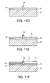
- the layer 62 is removed to a thickness making it possible to expose the deposited silicon 66, corresponding to the beam of the device ( figure 11D ).
- a layer 70 of SiO 2 is deposited on the structure thus obtained ( figure 11E ).
- another sacrificial layer made of a low density oxide for example, can be used.
- a layer 72 of polysilicon is deposited by LPCVD or a conductive material, for example AlSi, over a thickness of 1 .mu.m, for example.
- Conductive deposition for example AlSi
- Conductive deposition is then performed to obtain the corresponding contacts 74; and these contacts are formed by lithography and then etching ( figure 11F ).
- Part of the layer 72 is removed by lithography and etching ( figure 11G ).
- a layer 76 of silica is deposited on the structure obtained, for example more than 2 ⁇ m of SiO 2 , and then planarized by CMP, that is to say by a mechanical-chemical polishing process ( figure 11H ).
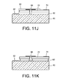
- a protective layer 80 of silica is deposited on the structure obtained, this layer 80 is locally removed by photolithography and successive etchings to redraw the contacts 74 as well as other contacts, such as the contact 82, which resulted from a first deposition-litho-etching of a metal layer at the beginning of the process ( figure 11J ).
- the silica layers are partially etched by means of hydrofluoric acid HF, to release the beam provided with the tray ( figure 11K ).
- a substrate 90 made of silicon is used and an asymmetrical piezoelectric stack 92 is formed on the substrate 90.
- a layer of molybdenum 94 is deposited therein, a lithography thereof is carried out, a layer is deposited on the substrate 90.
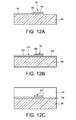
- 96 for example in AIN on the layer 94 a lithography is carried out thereof, a layer of molybdenum 98, for example, is deposited on the layer 96 and a lithography of this layer 98 is carried out ( figure 12A ).
- a layer 100 for example SiO 2 , 750 nm thick, for example, is deposited on the structure obtained. Lithography is performed to reveal the NEMS pattern 102 in the device ( figure 12B ).
- a layer 104 is deposited for example in silicon oxide ( figure 12C ).
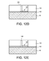
- the layer 104 is etched at the previously formed pattern 102 to define the location 106 of the beam of the device ( figure 12D ).
- this beam is deposited at this location, for example polysilicon 108 to the surface of the layer 104 ( figure 12E ).
- Polysilicon is deposited by LPCVD, over a thickness of 20 nm, for example, and lithography of this polysilicon is carried out to form the plate 110 of the device ( figure 12F ).
- the beam provided with its plate is liberated by wet etching of the resulting structure, using, for example, hydrofluoric acid ( figure 12G ).
- Devices according to the invention can also be produced by a co-integrated or "above IC” method as shown in FIG. figure 5 .
- the main constraint results from the use of cold thermal processes, that is to say processes carried out at temperatures below 500 ° C., or even below 300 ° C., in order to preserve the temperature. particular integrity of CMOS circuit and its interconnections.
- This process uses in particular a lower barrier layer, for example of HfO 2 or BN or SiN which is represented on the figure 5 .
- the epitaxy will then have to be replaced by cold deposits, for example conductive deposits of AlSi or W, followed by a chemical mechanical polishing (CMP) to keep the conductive material, only in the holes formed in the oxide (SiO 2 ).
- CMP chemical mechanical polishing
- Polysilicon deposits can also be replaced by metal deposits or deposits of amorphous silicon, possibly doped in situ. To obtain polysilicon from a low temperature deposition of amorphous silicon, laser annealing of the amorphous silicon can also be used to limit heating locally.
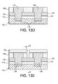
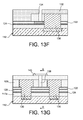
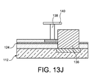
- FIGS. 13A to 13J schematically illustrate steps of such a method (after transfer to CMOS), making it possible to manufacture a device according to the invention.
- the figure 13A shows a CMOS plate 112. Only its last level “in metal” is represented.
- the reference 114 designates the metal zones of this plate 112 and the reference 115 denotes a dielectric layer, for example silica, allowing the realization of an oxide / oxide bonding.
- This structure 116 may be an SOI type substrate, comprising a bonding layer 117 of oxide, of 200 nm thick for example, a stop layer 124 of 10 nm to 100nm thick for example, a buried oxide 120, 400 nm thick for example, surmounted by a top layer 122 of silicon, 50 nm thick for example, previously doped with boron and activated.
- the oxide layer 117 allows molecular bonding with the layer 115.
- the meeting of the layers 115 and 117 has the reference 117a on the Figure 13B and the following ones.
- a layer of piezoelectric material could be used.
- stop layer 124 between the buried oxide 120 and the bonding layer 117 may be, for example, SiN, HfO 2 or BN.
- a 50 nm thick BN barrier layer is used.
- the structure 116 can also be obtained by successive deposits of appropriate layers.
- An insulating layer 126 of silica is then deposited on the upper layer 122 ( figure 13C ).
- a new photolithography and etching is carried out through the layer 126, to the metal zones 114, at the level of the etched areas of the layer 122 and the parts thus etched are eliminated through the layer 126, hence the openings 128.
- This second photolithography makes it possible to have a wider opening at the level of the layer 126, compared to that which was obtained by the preceding lithography (see the openings in the layer 122) and thus to reduce the contact resistance of the resumption of subsequent contact between the deposit 130 and the layer 122 (see FIG. figure 13D and the following ones).
- a layer 132 of silica is then deposited on the structure thus obtained ( figure 13E ). Then an opening 134 is formed which is substantially equidistant electrodes 130 in the example described, by photolithography and etching, to the upper layer 122 of silicon. This opening 134 is intended for the subsequent formation of a beam of the kind of the beam 8 of the figure 5 .
- the figure 13F shows the resulting structure, observed according to the AA section of the figure 13E as defined above. It shows an electrode 136 made of AlSi or Ti / TiN + W, which was formed at the same time as the electrodes 130, according to the same manufacturing steps. This electrode 136 is intended for actuating the beam that will be formed in the opening 134.
- the figure 13G illustrates the step of forming the beam 138, and the plate 140 which it is provided.
- the figure 13H shows the beam-tray assembly according to the AA section of the figure 13G . This set is obtained by depositing AlSi or HfO2 or any other equivalent material, such as BN for example, followed by etching to define the plate 140.
- figure 13I the beam 138, provided with its plate 140, is released by etching the resulting structure with hydrofluoric acid in the liquid or vapor state.
- the figure 13J illustrates this release according to the AA cut of the figure 13I .
- the electrical detection means In the case of a vertical device, made in thin layers, it is even less obvious to integrate the electrical detection means in the production method, in particular to small nanoscale dimensions. Indeed, the device is then produced in successive layers and the etching thereof as well as the good realization of the mechanical structure require to find ways to avoid misalignments between too large levels, typically of the same order of magnitude as the lateral dimensions of the device.
- the detection means measuring a displacement or a stress are based on very well controlled positioning between the mechanical structure and these means.
- the latter in the case where it is desired to have an "active" surface (for the detection of particles) above and covering the detection means, the latter must be much less bulky than the resonator itself, which limits strongly the possibilities.
Landscapes
- Physics & Mathematics (AREA)
- General Physics & Mathematics (AREA)
- Chemical & Material Sciences (AREA)
- Analytical Chemistry (AREA)
- Life Sciences & Earth Sciences (AREA)
- Health & Medical Sciences (AREA)
- Biochemistry (AREA)
- General Health & Medical Sciences (AREA)
- Immunology (AREA)
- Pathology (AREA)
- Acoustics & Sound (AREA)
- Dispersion Chemistry (AREA)
- Engineering & Computer Science (AREA)
- Power Engineering (AREA)
- Micromachines (AREA)
Applications Claiming Priority (1)
| Application Number | Priority Date | Filing Date | Title |
|---|---|---|---|
| FR1360281A FR3012124B1 (fr) | 2013-10-22 | 2013-10-22 | Dispositif de detection electromecanique, pour la detection gravimetrique, et procede de fabrication du dispositif |
Publications (2)
| Publication Number | Publication Date |
|---|---|
| EP2866020A1 true EP2866020A1 (de) | 2015-04-29 |
| EP2866020B1 EP2866020B1 (de) | 2023-02-22 |
Family
ID=50289758
Family Applications (1)
| Application Number | Title | Priority Date | Filing Date |
|---|---|---|---|
| EP14189689.4A Active EP2866020B1 (de) | 2013-10-22 | 2014-10-21 | Vorrichtung zur elektromechanischen Erfassung, zur gravimetrischen Erfassung |
Country Status (4)
| Country | Link |
|---|---|
| US (1) | US10670507B2 (de) |
| EP (1) | EP2866020B1 (de) |
| CN (1) | CN104555888A (de) |
| FR (1) | FR3012124B1 (de) |
Families Citing this family (4)
| Publication number | Priority date | Publication date | Assignee | Title |
|---|---|---|---|---|
| FR3046244A1 (fr) | 2015-12-23 | 2017-06-30 | Commissariat Energie Atomique | Capteur de gaz a selectivite amelioree et a compacite augmentee |
| FR3046153A1 (fr) | 2015-12-24 | 2017-06-30 | Commissariat Energie Atomique | Systeme presentant une densite surfacique de dispositfs microelectromecaniques et/ou nanoelectromecaniques augmentee |
| CN106990016A (zh) * | 2017-04-21 | 2017-07-28 | 上海赛菲环境科技股份有限公司 | 一种粉尘传感器 |
| CN108132085B (zh) * | 2017-12-21 | 2019-05-28 | 山东理工大学 | 一种基于隧道效应的纳微质量测量装置与方法 |
Citations (6)
| Publication number | Priority date | Publication date | Assignee | Title |
|---|---|---|---|---|
| US20060086174A1 (en) * | 2004-10-21 | 2006-04-27 | David Korpi | Oscillating Inertial Microbalance and Method of Passive Compensation |
| US20100041091A1 (en) | 2008-02-05 | 2010-02-18 | California Institute Of Technology | Microfluidic embedded polymer nems force sensors |
| FR2961016A1 (fr) | 2010-06-07 | 2011-12-09 | Commissariat Energie Atomique | Circuit integre a dispositif de type fet sans jonction et a depletion |
| WO2012034951A1 (fr) | 2010-09-13 | 2012-03-22 | Commissariat à l'énergie atomique et aux énergies alternatives | Dispositif a poutre suspendue et moyens de detection piezoresistive du deplacement de celle-ci, et procede de fabrication du dispositif |
| WO2012034949A1 (fr) | 2010-09-13 | 2012-03-22 | Commissariat à l'énergie atomique et aux énergies alternatives | Dispositif resonant a actionnement dans le plan, et procede de fabrication du dispositif |
| WO2012034990A1 (fr) | 2010-09-13 | 2012-03-22 | Commissariat à l'énergie atomique et aux énergies alternatives | Dispositif resonant, a detection piezoresistive et a resonateur relie de facon elastique au support du dispositif, et procede de fabrication de celui-ci |
Family Cites Families (12)
| Publication number | Priority date | Publication date | Assignee | Title |
|---|---|---|---|---|
| US5162691A (en) * | 1991-01-22 | 1992-11-10 | The United States Of America As Represented By The Secretary Of The Army | Cantilevered air-gap type thin film piezoelectric resonator |
| JP4176450B2 (ja) * | 2002-02-13 | 2008-11-05 | 松下電器産業株式会社 | 微小機械振動フィルタ |
| US6909824B1 (en) | 2002-03-05 | 2005-06-21 | Avi Messica | Mechanically actuated evanescent-wave coupled optical devices |
| US20060257286A1 (en) * | 2003-10-17 | 2006-11-16 | Adams Jesse D | Self-sensing array of microcantilevers for chemical detection |
| JP4754817B2 (ja) * | 2004-12-20 | 2011-08-24 | Okiセミコンダクタ株式会社 | 半導体加速度センサ |
| US7120332B1 (en) | 2005-03-31 | 2006-10-10 | Eastman Kodak Company | Placement of lumiphores within a light emitting resonator in a visual display with electro-optical addressing architecture |
| CN101490539A (zh) * | 2006-05-10 | 2009-07-22 | 德雷塞尔大学 | 直接在空气中检测空气传播的分析物的自励自感式压电悬臂传感器 |
| WO2012033837A2 (en) * | 2010-09-08 | 2012-03-15 | Micropen Technologies Corporation | Pressure sensing or force generating device |
| US8925385B2 (en) * | 2010-12-06 | 2015-01-06 | Sierra Instruments, Inc. | Longitudinal resonating mode inertial mass sensing systems |
| FR3003083B1 (fr) | 2013-03-11 | 2015-04-10 | Commissariat Energie Atomique | Dispositif de determination de la masse d'une particule en suspension ou en solution dans un fluide |
| CN103207004B (zh) * | 2013-04-12 | 2015-11-25 | 昆山禾信质谱技术有限公司 | 基于微振荡法测量颗粒物质量的装置 |
| EP2866000B1 (de) * | 2013-10-22 | 2020-03-11 | Commissariat à l'Énergie Atomique et aux Énergies Alternatives | Optomechanische Vorrichtung zum Betätigen und/oder Erkennen einer Bewegung eines mechanischen Elements, insbesondere für die gravimetrische Erfassung |
-
2013
- 2013-10-22 FR FR1360281A patent/FR3012124B1/fr active Active
-
2014
- 2014-10-21 US US14/519,353 patent/US10670507B2/en active Active
- 2014-10-21 EP EP14189689.4A patent/EP2866020B1/de active Active
- 2014-10-22 CN CN201410567514.5A patent/CN104555888A/zh active Pending
Patent Citations (6)
| Publication number | Priority date | Publication date | Assignee | Title |
|---|---|---|---|---|
| US20060086174A1 (en) * | 2004-10-21 | 2006-04-27 | David Korpi | Oscillating Inertial Microbalance and Method of Passive Compensation |
| US20100041091A1 (en) | 2008-02-05 | 2010-02-18 | California Institute Of Technology | Microfluidic embedded polymer nems force sensors |
| FR2961016A1 (fr) | 2010-06-07 | 2011-12-09 | Commissariat Energie Atomique | Circuit integre a dispositif de type fet sans jonction et a depletion |
| WO2012034951A1 (fr) | 2010-09-13 | 2012-03-22 | Commissariat à l'énergie atomique et aux énergies alternatives | Dispositif a poutre suspendue et moyens de detection piezoresistive du deplacement de celle-ci, et procede de fabrication du dispositif |
| WO2012034949A1 (fr) | 2010-09-13 | 2012-03-22 | Commissariat à l'énergie atomique et aux énergies alternatives | Dispositif resonant a actionnement dans le plan, et procede de fabrication du dispositif |
| WO2012034990A1 (fr) | 2010-09-13 | 2012-03-22 | Commissariat à l'énergie atomique et aux énergies alternatives | Dispositif resonant, a detection piezoresistive et a resonateur relie de facon elastique au support du dispositif, et procede de fabrication de celui-ci |
Non-Patent Citations (12)
| Title |
|---|
| A.K. NAIK; M.S. HANAY; W. K. HIEBERT; X. L. FENG; M. L. ROUKES: "Towards single-molecule nanomechanical mass spectrometry", NATURE NANOTECHNOLOGY, vol. 4, 2009, pages 445 - 450, XP055024639, DOI: doi:10.1038/nnano.2009.152 |
| BARGATIN, E.B. MYERS; J. S. ALDRIDGE; C. MARCOUX; P. BRIANCEAU; L. DURAFFOURG; E. COLINET; S. HENTZ; P. ANDREUCCI; M.L. ROUKES: "Large-scale integration of nanoelectromechanical systems for gas sensing applications", NANO LETTERS, vol. 12, no. 3, 14 March 2012 (2012-03-14), pages 1269 - 74, XP055047111, DOI: doi:10.1021/nl2037479 |
| E. MILE; G. JOURDAN; 1. BARGATIN; S. LABARTHE; C. MARCOUX; P. ANDREUCCI; S. HENTZ; C. KHARRAT; E. COLINET; L. DURAFFOURG: "In-plane nanoelectromechanical resonators based on silicon nanowire piezoresistive detection", NANOTECHNOLOGY, vol. 21, no. 16, 21 April 2010 (2010-04-21), pages 165504, XP020174814 |
| J. CHASTE; A. EICHLER; J. MOSER; G. CEBALLOS; R. RURALI; A. BACHTOLD: "A nanomechanical mass sensor with yoctogram resolution", NATURE NANOTECHNOLOGY, vol. 7, 2012, pages 301 - 304 |
| K.L. EKINCI; Y. T. TANG; M. L. ROUKES: "Ultimate limits to inertial mass sensing based upon nanoelectromechanical systems", JOURNAL OF APPLIED PHYSICS, vol. 95, no. 5, 2004, pages 2682, XP012067540, DOI: doi:10.1063/1.1642738 |
| KEHRBUSCH J ET AL: "Columnar shaped microresonators for mass detection and gas analysis", MICROELECTRONIC ENGINEERING, ELSEVIER PUBLISHERS BV., AMSTERDAM, NL, vol. 87, no. 5-8, 23 November 2009 (2009-11-23), pages 817 - 820, XP026945313, ISSN: 0167-9317, [retrieved on 20091123], DOI: 10.1016/J.MEE.2009.11.075 * |
| KEHRBUSCH J ET AL: "High frequency columnar silicon microresonators for mass detection", APPLIED PHYSICS LETTERS, AMERICAN INSTITUTE OF PHYSICS, US, vol. 93, no. 2, 14 July 2008 (2008-07-14), pages 23102-1 - 23102-3, XP012112462, ISSN: 0003-6951, DOI: 10.1063/1.2957653 * |
| MO LI; H.X. TANG; M. L. ROUKES: "Ultra-sensitive NEMS-based cantilevers for sensing, scanned probe and very high-frequency applications", NATURE NANOTECHNOLOGY, vol. 2, no. 2, February 2007 (2007-02-01), pages 114 - 20, XP002567868, DOI: doi:10.1038/nnano.2006.208 |
| P. IVALDI; J. ABERGEL; M. H. MATHENY; L. G. VILLANUEVA; R.B. KARABALIN; M. L. ROUKES; P. ANDREUCCI; S. HENTZ; E. DEFAŸ: "50 nm thick AIN film-based piezoelectric cantilevers for gravimetric detection", JOURNAL OF MICROMECHANICS AND MICROENGINEERING, vol. 21, 2011, pages 085023 |
| S. DOHN; W. SVENDSEN; A. BOISEN; O. HANSEN: "Mass and position determination of attached particles on cantilever based mass sensors", REVIEW OF SCIENTIFIC INSTRUMENTS, vol. 78, 2007, pages 103303, XP012103641, DOI: doi:10.1063/1.2804074 |
| S. GUILLON; S. SALOMON; F. SEICHEPINE; D. DEZEST; F. MATHIEU; A. BOUCHIER; L. MAZENQ; C. THIBAULT; C. VIEU; T. LEÏCHLÉ: "Biological functionalization of massively parallel arrays of nanocantilevers using microcontact printing", SENSORS AND ACTUATORS B: CHEMICAL, vol. 161, January 2012 (2012-01-01), pages 1135 - 1138, XP028447849, DOI: doi:10.1016/j.snb.2011.10.084 |
| TOFFOLI VALERIA ET AL: "Actuation of silicon pillar micro-mechanical resonators by Kelvin polarization force", MICROELECTRONIC ENGINEERING, vol. 111, 30 May 2013 (2013-05-30), pages 1 - 6, XP028673648, ISSN: 0167-9317, DOI: 10.1016/J.MEE.2013.05.013 * |
Also Published As
| Publication number | Publication date |
|---|---|
| FR3012124A1 (fr) | 2015-04-24 |
| EP2866020B1 (de) | 2023-02-22 |
| CN104555888A (zh) | 2015-04-29 |
| US20150107336A1 (en) | 2015-04-23 |
| US10670507B2 (en) | 2020-06-02 |
| FR3012124B1 (fr) | 2017-12-15 |
Similar Documents
| Publication | Publication Date | Title |
|---|---|---|
| EP2866000B1 (de) | Optomechanische Vorrichtung zum Betätigen und/oder Erkennen einer Bewegung eines mechanischen Elements, insbesondere für die gravimetrische Erfassung | |
| EP2211185B1 (de) | Trägheitssensor oder Resonanzsensor in der Oberflächentechnologie zur Erkennung von Abweichungen mit Hilfe eines Dehnungsmessers | |
| EP2309559B1 (de) | Piezoelektrische Erregerstruktur mit integriertem piezoresistivem Dehnmessstreifen und Herstellungsverfahren dafür | |
| EP2211143B1 (de) | Planarer mikromechanischer Kreisel mit Messung ausserhalb der Ebene mittels Dehnungsmesser | |
| US20200244243A1 (en) | Graphene microelectromechanical system (mems) resonant gas sensor | |
| EP2233919B1 (de) | Mikrovorrichtung zum In-Situ-Nachweis von bestimmten Partikeln in einem flüssigen Medium, und Verfahren zu dessen Ausführung | |
| EP2617129B1 (de) | Vorrichtung mit freihängendem träger und piezoresistive vorrichtung zur verlagerungserkennung | |
| EP3325981B1 (de) | Sonde für rasterkraftmikroskop mit kleiner grösse und diese sonde enthaltendes rasterkraftmikroskop | |
| EP1840582A1 (de) | Resonanter Trägheitsmikrosensor variabler Dicke, der im Bereich der Oberflächentechnologien eingesetzt wird | |
| EP2616386B1 (de) | In der ebene betätigte resonanzvorrichtung und verfahren zur herstellung der vorrichtung | |
| EP2866020B1 (de) | Vorrichtung zur elektromechanischen Erfassung, zur gravimetrischen Erfassung | |
| EP1960307A1 (de) | Mikroelektromechanisches system mit einem verformbaren teil und einem belastungssensor | |
| EP2949621B1 (de) | Kapazitive mikro- und/ oder nanoelektronische Vorrichtung mit erhöhter Kompaktheit | |
| WO2009141515A1 (fr) | Dispositif pour la detection gravimetrique de particules en milieu fluide comprenant un oscillateur entre deux canaux fluidiques, procede de realisation et methode de mise en oeuvre du dispositif | |
| CA2445285C (fr) | Matrice de biocapteurs et son procede de fabrication | |
| EP3312616B1 (de) | Miniaturisierte sonde für rasterkraftmikroskopie mit geringem platzbedarf | |
| FR2916271A1 (fr) | Circuit electronique permettant la mesure de masse de materiau biologique et procede de fabrication | |
| Alava et al. | Piezoelectric-actuated, piezoresistive-sensed circular micromembranes for label-free biosensing applications | |
| WO2005081929A2 (en) | Detection of resonator motion using piezoresistive signal downmixing |
Legal Events
| Date | Code | Title | Description |
|---|---|---|---|
| PUAI | Public reference made under article 153(3) epc to a published international application that has entered the european phase |
Free format text: ORIGINAL CODE: 0009012 |
|
| 17P | Request for examination filed |
Effective date: 20141021 |
|
| AK | Designated contracting states |
Kind code of ref document: A1 Designated state(s): AL AT BE BG CH CY CZ DE DK EE ES FI FR GB GR HR HU IE IS IT LI LT LU LV MC MK MT NL NO PL PT RO RS SE SI SK SM TR |
|
| AX | Request for extension of the european patent |
Extension state: BA ME |
|
| R17P | Request for examination filed (corrected) |
Effective date: 20151028 |
|
| RBV | Designated contracting states (corrected) |
Designated state(s): AL AT BE BG CH CY CZ DE DK EE ES FI FR GB GR HR HU IE IS IT LI LT LU LV MC MK MT NL NO PL PT RO RS SE SI SK SM TR |
|
| STAA | Information on the status of an ep patent application or granted ep patent |
Free format text: STATUS: EXAMINATION IS IN PROGRESS |
|
| 17Q | First examination report despatched |
Effective date: 20190717 |
|
| RIC1 | Information provided on ipc code assigned before grant |
Ipc: G01N 29/036 20060101ALI20220718BHEP Ipc: G01L 1/22 20060101ALI20220718BHEP Ipc: G01L 1/18 20060101ALI20220718BHEP Ipc: G01L 1/14 20060101ALI20220718BHEP Ipc: G01N 29/02 20060101ALI20220718BHEP Ipc: G01N 5/02 20060101AFI20220718BHEP |
|
| GRAP | Despatch of communication of intention to grant a patent |
Free format text: ORIGINAL CODE: EPIDOSNIGR1 |
|
| STAA | Information on the status of an ep patent application or granted ep patent |
Free format text: STATUS: GRANT OF PATENT IS INTENDED |
|
| INTG | Intention to grant announced |
Effective date: 20220915 |
|
| GRAS | Grant fee paid |
Free format text: ORIGINAL CODE: EPIDOSNIGR3 |
|
| GRAA | (expected) grant |
Free format text: ORIGINAL CODE: 0009210 |
|
| STAA | Information on the status of an ep patent application or granted ep patent |
Free format text: STATUS: THE PATENT HAS BEEN GRANTED |
|
| AK | Designated contracting states |
Kind code of ref document: B1 Designated state(s): AL AT BE BG CH CY CZ DE DK EE ES FI FR GB GR HR HU IE IS IT LI LT LU LV MC MK MT NL NO PL PT RO RS SE SI SK SM TR |
|
| REG | Reference to a national code |
Ref country code: GB Ref legal event code: FG4D Free format text: NOT ENGLISH |
|
| REG | Reference to a national code |
Ref country code: CH Ref legal event code: EP |
|
| REG | Reference to a national code |
Ref country code: DE Ref legal event code: R096 Ref document number: 602014086264 Country of ref document: DE |
|
| REG | Reference to a national code |
Ref country code: AT Ref legal event code: REF Ref document number: 1549808 Country of ref document: AT Kind code of ref document: T Effective date: 20230315 Ref country code: IE Ref legal event code: FG4D Free format text: LANGUAGE OF EP DOCUMENT: FRENCH |
|
| REG | Reference to a national code |
Ref country code: NL Ref legal event code: FP |
|
| REG | Reference to a national code |
Ref country code: LT Ref legal event code: MG9D |
|
| REG | Reference to a national code |
Ref country code: AT Ref legal event code: MK05 Ref document number: 1549808 Country of ref document: AT Kind code of ref document: T Effective date: 20230222 |
|
| PG25 | Lapsed in a contracting state [announced via postgrant information from national office to epo] |
Ref country code: RS Free format text: LAPSE BECAUSE OF FAILURE TO SUBMIT A TRANSLATION OF THE DESCRIPTION OR TO PAY THE FEE WITHIN THE PRESCRIBED TIME-LIMIT Effective date: 20230222 Ref country code: PT Free format text: LAPSE BECAUSE OF FAILURE TO SUBMIT A TRANSLATION OF THE DESCRIPTION OR TO PAY THE FEE WITHIN THE PRESCRIBED TIME-LIMIT Effective date: 20230622 Ref country code: NO Free format text: LAPSE BECAUSE OF FAILURE TO SUBMIT A TRANSLATION OF THE DESCRIPTION OR TO PAY THE FEE WITHIN THE PRESCRIBED TIME-LIMIT Effective date: 20230522 Ref country code: LV Free format text: LAPSE BECAUSE OF FAILURE TO SUBMIT A TRANSLATION OF THE DESCRIPTION OR TO PAY THE FEE WITHIN THE PRESCRIBED TIME-LIMIT Effective date: 20230222 Ref country code: LT Free format text: LAPSE BECAUSE OF FAILURE TO SUBMIT A TRANSLATION OF THE DESCRIPTION OR TO PAY THE FEE WITHIN THE PRESCRIBED TIME-LIMIT Effective date: 20230222 Ref country code: HR Free format text: LAPSE BECAUSE OF FAILURE TO SUBMIT A TRANSLATION OF THE DESCRIPTION OR TO PAY THE FEE WITHIN THE PRESCRIBED TIME-LIMIT Effective date: 20230222 Ref country code: ES Free format text: LAPSE BECAUSE OF FAILURE TO SUBMIT A TRANSLATION OF THE DESCRIPTION OR TO PAY THE FEE WITHIN THE PRESCRIBED TIME-LIMIT Effective date: 20230222 Ref country code: AT Free format text: LAPSE BECAUSE OF FAILURE TO SUBMIT A TRANSLATION OF THE DESCRIPTION OR TO PAY THE FEE WITHIN THE PRESCRIBED TIME-LIMIT Effective date: 20230222 |
|
| PG25 | Lapsed in a contracting state [announced via postgrant information from national office to epo] |
Ref country code: SE Free format text: LAPSE BECAUSE OF FAILURE TO SUBMIT A TRANSLATION OF THE DESCRIPTION OR TO PAY THE FEE WITHIN THE PRESCRIBED TIME-LIMIT Effective date: 20230222 Ref country code: PL Free format text: LAPSE BECAUSE OF FAILURE TO SUBMIT A TRANSLATION OF THE DESCRIPTION OR TO PAY THE FEE WITHIN THE PRESCRIBED TIME-LIMIT Effective date: 20230222 Ref country code: IS Free format text: LAPSE BECAUSE OF FAILURE TO SUBMIT A TRANSLATION OF THE DESCRIPTION OR TO PAY THE FEE WITHIN THE PRESCRIBED TIME-LIMIT Effective date: 20230622 Ref country code: GR Free format text: LAPSE BECAUSE OF FAILURE TO SUBMIT A TRANSLATION OF THE DESCRIPTION OR TO PAY THE FEE WITHIN THE PRESCRIBED TIME-LIMIT Effective date: 20230523 Ref country code: FI Free format text: LAPSE BECAUSE OF FAILURE TO SUBMIT A TRANSLATION OF THE DESCRIPTION OR TO PAY THE FEE WITHIN THE PRESCRIBED TIME-LIMIT Effective date: 20230222 |
|
| PG25 | Lapsed in a contracting state [announced via postgrant information from national office to epo] |
Ref country code: SM Free format text: LAPSE BECAUSE OF FAILURE TO SUBMIT A TRANSLATION OF THE DESCRIPTION OR TO PAY THE FEE WITHIN THE PRESCRIBED TIME-LIMIT Effective date: 20230222 Ref country code: RO Free format text: LAPSE BECAUSE OF FAILURE TO SUBMIT A TRANSLATION OF THE DESCRIPTION OR TO PAY THE FEE WITHIN THE PRESCRIBED TIME-LIMIT Effective date: 20230222 Ref country code: EE Free format text: LAPSE BECAUSE OF FAILURE TO SUBMIT A TRANSLATION OF THE DESCRIPTION OR TO PAY THE FEE WITHIN THE PRESCRIBED TIME-LIMIT Effective date: 20230222 Ref country code: DK Free format text: LAPSE BECAUSE OF FAILURE TO SUBMIT A TRANSLATION OF THE DESCRIPTION OR TO PAY THE FEE WITHIN THE PRESCRIBED TIME-LIMIT Effective date: 20230222 Ref country code: CZ Free format text: LAPSE BECAUSE OF FAILURE TO SUBMIT A TRANSLATION OF THE DESCRIPTION OR TO PAY THE FEE WITHIN THE PRESCRIBED TIME-LIMIT Effective date: 20230222 |
|
| REG | Reference to a national code |
Ref country code: DE Ref legal event code: R097 Ref document number: 602014086264 Country of ref document: DE |
|
| PG25 | Lapsed in a contracting state [announced via postgrant information from national office to epo] |
Ref country code: SK Free format text: LAPSE BECAUSE OF FAILURE TO SUBMIT A TRANSLATION OF THE DESCRIPTION OR TO PAY THE FEE WITHIN THE PRESCRIBED TIME-LIMIT Effective date: 20230222 |
|
| PLBE | No opposition filed within time limit |
Free format text: ORIGINAL CODE: 0009261 |
|
| STAA | Information on the status of an ep patent application or granted ep patent |
Free format text: STATUS: NO OPPOSITION FILED WITHIN TIME LIMIT |
|
| 26N | No opposition filed |
Effective date: 20231123 |
|
| PG25 | Lapsed in a contracting state [announced via postgrant information from national office to epo] |
Ref country code: SI Free format text: LAPSE BECAUSE OF FAILURE TO SUBMIT A TRANSLATION OF THE DESCRIPTION OR TO PAY THE FEE WITHIN THE PRESCRIBED TIME-LIMIT Effective date: 20230222 |
|
| PG25 | Lapsed in a contracting state [announced via postgrant information from national office to epo] |
Ref country code: IT Free format text: LAPSE BECAUSE OF FAILURE TO SUBMIT A TRANSLATION OF THE DESCRIPTION OR TO PAY THE FEE WITHIN THE PRESCRIBED TIME-LIMIT Effective date: 20230222 Ref country code: MC Free format text: LAPSE BECAUSE OF FAILURE TO SUBMIT A TRANSLATION OF THE DESCRIPTION OR TO PAY THE FEE WITHIN THE PRESCRIBED TIME-LIMIT Effective date: 20230222 |
|
| REG | Reference to a national code |
Ref country code: CH Ref legal event code: PL |
|
| PG25 | Lapsed in a contracting state [announced via postgrant information from national office to epo] |
Ref country code: LU Free format text: LAPSE BECAUSE OF NON-PAYMENT OF DUE FEES Effective date: 20231021 |
|
| PG25 | Lapsed in a contracting state [announced via postgrant information from national office to epo] |
Ref country code: LU Free format text: LAPSE BECAUSE OF NON-PAYMENT OF DUE FEES Effective date: 20231021 |
|
| PG25 | Lapsed in a contracting state [announced via postgrant information from national office to epo] |
Ref country code: CH Free format text: LAPSE BECAUSE OF NON-PAYMENT OF DUE FEES Effective date: 20231031 |
|
| PG25 | Lapsed in a contracting state [announced via postgrant information from national office to epo] |
Ref country code: CH Free format text: LAPSE BECAUSE OF NON-PAYMENT OF DUE FEES Effective date: 20231031 |
|
| PG25 | Lapsed in a contracting state [announced via postgrant information from national office to epo] |
Ref country code: IE Free format text: LAPSE BECAUSE OF NON-PAYMENT OF DUE FEES Effective date: 20231021 |
|
| PG25 | Lapsed in a contracting state [announced via postgrant information from national office to epo] |
Ref country code: IE Free format text: LAPSE BECAUSE OF NON-PAYMENT OF DUE FEES Effective date: 20231021 |
|
| PG25 | Lapsed in a contracting state [announced via postgrant information from national office to epo] |
Ref country code: BG Free format text: LAPSE BECAUSE OF FAILURE TO SUBMIT A TRANSLATION OF THE DESCRIPTION OR TO PAY THE FEE WITHIN THE PRESCRIBED TIME-LIMIT Effective date: 20230222 |
|
| PG25 | Lapsed in a contracting state [announced via postgrant information from national office to epo] |
Ref country code: BG Free format text: LAPSE BECAUSE OF FAILURE TO SUBMIT A TRANSLATION OF THE DESCRIPTION OR TO PAY THE FEE WITHIN THE PRESCRIBED TIME-LIMIT Effective date: 20230222 |
|
| PG25 | Lapsed in a contracting state [announced via postgrant information from national office to epo] |
Ref country code: CY Free format text: LAPSE BECAUSE OF FAILURE TO SUBMIT A TRANSLATION OF THE DESCRIPTION OR TO PAY THE FEE WITHIN THE PRESCRIBED TIME-LIMIT; INVALID AB INITIO Effective date: 20141021 |
|
| PG25 | Lapsed in a contracting state [announced via postgrant information from national office to epo] |
Ref country code: HU Free format text: LAPSE BECAUSE OF FAILURE TO SUBMIT A TRANSLATION OF THE DESCRIPTION OR TO PAY THE FEE WITHIN THE PRESCRIBED TIME-LIMIT; INVALID AB INITIO Effective date: 20141021 |
|
| PGFP | Annual fee paid to national office [announced via postgrant information from national office to epo] |
Ref country code: NL Payment date: 20251023 Year of fee payment: 12 |
|
| PG25 | Lapsed in a contracting state [announced via postgrant information from national office to epo] |
Ref country code: TR Free format text: LAPSE BECAUSE OF FAILURE TO SUBMIT A TRANSLATION OF THE DESCRIPTION OR TO PAY THE FEE WITHIN THE PRESCRIBED TIME-LIMIT Effective date: 20230222 |
|
| PGFP | Annual fee paid to national office [announced via postgrant information from national office to epo] |
Ref country code: DE Payment date: 20251020 Year of fee payment: 12 |
|
| PGFP | Annual fee paid to national office [announced via postgrant information from national office to epo] |
Ref country code: GB Payment date: 20251029 Year of fee payment: 12 |
|
| PGFP | Annual fee paid to national office [announced via postgrant information from national office to epo] |
Ref country code: FR Payment date: 20251024 Year of fee payment: 12 |
|
| PGFP | Annual fee paid to national office [announced via postgrant information from national office to epo] |
Ref country code: BE Payment date: 20251022 Year of fee payment: 12 |