EP1840582A1 - Resonanter Trägheitsmikrosensor variabler Dicke, der im Bereich der Oberflächentechnologien eingesetzt wird - Google Patents
Resonanter Trägheitsmikrosensor variabler Dicke, der im Bereich der Oberflächentechnologien eingesetzt wird Download PDFInfo
- Publication number
- EP1840582A1 EP1840582A1 EP07104737A EP07104737A EP1840582A1 EP 1840582 A1 EP1840582 A1 EP 1840582A1 EP 07104737 A EP07104737 A EP 07104737A EP 07104737 A EP07104737 A EP 07104737A EP 1840582 A1 EP1840582 A1 EP 1840582A1
- Authority
- EP
- European Patent Office
- Prior art keywords
- zone
- thickness
- sensor
- resonator
- sensor according
- Prior art date
- Legal status (The legal status is an assumption and is not a legal conclusion. Google has not performed a legal analysis and makes no representation as to the accuracy of the status listed.)
- Granted
Links
Images



Classifications
-
- G—PHYSICS
- G01—MEASURING; TESTING
- G01P—MEASURING LINEAR OR ANGULAR SPEED, ACCELERATION, DECELERATION, OR SHOCK; INDICATING PRESENCE, ABSENCE, OR DIRECTION, OF MOVEMENT
- G01P15/00—Measuring acceleration; Measuring deceleration; Measuring shock, i.e. sudden change of acceleration
- G01P15/02—Measuring acceleration; Measuring deceleration; Measuring shock, i.e. sudden change of acceleration by making use of inertia forces using solid seismic masses
- G01P15/08—Measuring acceleration; Measuring deceleration; Measuring shock, i.e. sudden change of acceleration by making use of inertia forces using solid seismic masses with conversion into electric or magnetic values
- G01P15/097—Measuring acceleration; Measuring deceleration; Measuring shock, i.e. sudden change of acceleration by making use of inertia forces using solid seismic masses with conversion into electric or magnetic values by vibratory elements
-
- G—PHYSICS
- G01—MEASURING; TESTING
- G01C—MEASURING DISTANCES, LEVELS OR BEARINGS; SURVEYING; NAVIGATION; GYROSCOPIC INSTRUMENTS; PHOTOGRAMMETRY OR VIDEOGRAMMETRY
- G01C19/00—Gyroscopes; Turn-sensitive devices using vibrating masses; Turn-sensitive devices without moving masses; Measuring angular rate using gyroscopic effects
- G01C19/56—Turn-sensitive devices using vibrating masses, e.g. vibratory angular rate sensors based on Coriolis forces
- G01C19/5719—Turn-sensitive devices using vibrating masses, e.g. vibratory angular rate sensors based on Coriolis forces using planar vibrating masses driven in a translation vibration along an axis
- G01C19/5733—Structural details or topology
- G01C19/574—Structural details or topology the devices having two sensing masses in anti-phase motion
-
- G—PHYSICS
- G01—MEASURING; TESTING
- G01C—MEASURING DISTANCES, LEVELS OR BEARINGS; SURVEYING; NAVIGATION; GYROSCOPIC INSTRUMENTS; PHOTOGRAMMETRY OR VIDEOGRAMMETRY
- G01C19/00—Gyroscopes; Turn-sensitive devices using vibrating masses; Turn-sensitive devices without moving masses; Measuring angular rate using gyroscopic effects
- G01C19/56—Turn-sensitive devices using vibrating masses, e.g. vibratory angular rate sensors based on Coriolis forces
- G01C19/5719—Turn-sensitive devices using vibrating masses, e.g. vibratory angular rate sensors based on Coriolis forces using planar vibrating masses driven in a translation vibration along an axis
- G01C19/5733—Structural details or topology
- G01C19/5755—Structural details or topology the devices having a single sensing mass
-
- G—PHYSICS
- G01—MEASURING; TESTING
- G01C—MEASURING DISTANCES, LEVELS OR BEARINGS; SURVEYING; NAVIGATION; GYROSCOPIC INSTRUMENTS; PHOTOGRAMMETRY OR VIDEOGRAMMETRY
- G01C19/00—Gyroscopes; Turn-sensitive devices using vibrating masses; Turn-sensitive devices without moving masses; Measuring angular rate using gyroscopic effects
- G01C19/56—Turn-sensitive devices using vibrating masses, e.g. vibratory angular rate sensors based on Coriolis forces
- G01C19/5719—Turn-sensitive devices using vibrating masses, e.g. vibratory angular rate sensors based on Coriolis forces using planar vibrating masses driven in a translation vibration along an axis
- G01C19/5769—Manufacturing; Mounting; Housings
-
- G—PHYSICS
- G01—MEASURING; TESTING
- G01P—MEASURING LINEAR OR ANGULAR SPEED, ACCELERATION, DECELERATION, OR SHOCK; INDICATING PRESENCE, ABSENCE, OR DIRECTION, OF MOVEMENT
- G01P15/00—Measuring acceleration; Measuring deceleration; Measuring shock, i.e. sudden change of acceleration
- G01P15/02—Measuring acceleration; Measuring deceleration; Measuring shock, i.e. sudden change of acceleration by making use of inertia forces using solid seismic masses
- G01P15/08—Measuring acceleration; Measuring deceleration; Measuring shock, i.e. sudden change of acceleration by making use of inertia forces using solid seismic masses with conversion into electric or magnetic values
- G01P15/0802—Details
Definitions
- the invention relates to the field of micro-sensors, in particular silicon, for example inertial sensors, including accelerometers or gyrometers.
- Inertial sensors made in volume technology are based on off-plane electrostatic excitation of the resonator. As a result, they require the transfer of 2 substrates, one of which serves to produce the excitation / detection electrode (s) and the second serves to close the vacuum cavity. The technologies involved are therefore heavy.
- the resonator then has a thickness different from the seismic mass. This thinning is, among other things, made necessary by the vibration mode of the beam which is off plan.
- the resonator is placed on the surface of the substrate.
- the resonator should be as close as possible to the hinge (axis of rotation of the mass).
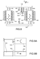
- FIGS. 9A and 9B respectively in plan view and in sectional view.
- an axis XX '201 is the sensitive axis of the sensor.
- References 202, 204, 206 respectively denote a seismic mass, a resonator, and a hinge. The sectional view shows that the mass 202 and the resonator 204 have the same thickness.
- the sensitive element 202 has a surface (in top view) of the order of mm 2 .
- a first approach is to postpone the MEMS on the MOS circuit once realized.
- the MEMS is in this case made by deposited layers.
- the metrological performances of the sensors thus produced are then quite limited, since the mechanical properties of the deposited materials are quite low compared to what is used when using the monocrystalline Si.
- the "In IC” approach consists in making the MEMS at the same level as the CMOS circuits. In this case, it is possible to have access to the Si monocrystalline to achieve the MEMS and thus obtain good performance.
- the homothetic miniaturization results in a "relative stiffening" of the mechanical structure with respect to the forces of inertia.
- the invention proposes making MEMS sensors with resonator detection using a "3D" planar technology.
- the invention relates to a resonant MEMS sensor in surface technology and excitation of the resonator in a plane, with multiple thicknesses. It is for example an accelerometer or a gyrometer. Typically one can have 2 different thicknesses on the same component, but also more than two thicknesses, for example three.
- a first thick zone has a first thickness and is used for the seismic mass part, for example an accelerometer or a gyrometer.
- a second zone, thin has a second thickness less than the first. The ratio between these two thicknesses is for example between 2 and 10. The second zone is used for the detection and possibly for the production of the hinges (or a torsion axis in the case of a gyroscope).
- the design of the resonant sensors made in surface technology is modified by decorrelating the seismic mass part of the detection part.
- the first zone preferably has a surface S less than 0.1 mm 2 for an accelerometer, and less than 5 mm 2 for a gyrometer.
- the first and second regions may be formed in the superficial semiconductor layer of an SOI substrate.
- a sensor according to the invention may further comprise a third hinge zone (or a torsion axis in the case of a gyrometer), this third zone having a thickness between that of the first zone and that of the second zone, or equal to that of the first zone, or equal to that of the second zone.
- Mechanical stops may be provided to limit the displacement of the seismic mass.
- Digital detection means may also be provided, for example comprising digital filtering means and / or digital signal processing.
- the invention also relates to a method for producing a device according to the invention, implementing differentiated etching steps, in depth, perpendicularly to a plane of the seismic mass, first and / or second and / or third areas.
- the thick zone and the thin zone may be formed by etching a layer of semiconductor material, in 3 dimensions.
- They can be formed by etching a superficial layer of semiconductor material of an SOI substrate in a direction (z) perpendicular to a main plane of this SOI substrate.
- Such a method may furthermore comprise the formation of a third zone, called the hinge zone or torsion axis, of thickness lying between that of the first zone and that of the second zone, or equal to one of the thicknesses of these zones. two areas.
- a third zone called the hinge zone or torsion axis
- the thin zone is formed in a semiconductor surface layer, the thick zone being made in an epitaxial semiconductor layer on said surface layer and in this superficial layer.
- Such a sensor 100 may be for example an accelerometer or a gyrometer. It's about of a sensor in surface technology and excitation of the resonator in a plane.
- an axis XX '1 is the sensitive axis of the sensor.
- References 2, 4 respectively denote a seismic mass, a resonator.
- the reference 6 designates a hinge in the case of an accelerometer and a torsion axis in the case of a gyrometer (a gyrometer is described below in connection with FIG. 8).
- the sectional view (FIG. 1B) shows that the mass 2 and the resonator 4 do not have the same thickness: the mass 2 has a first thickness E 1 , for example of the order of 1 ⁇ m, greater than the thickness E 2 of the resonator.
- the ratio E 1 / E 2 is for example between 2 and 10.
- the hinge makes it possible to maintain the seismic mass in the same plane, that of FIG. 1A or else that defined by the seismic mass 2, the dimensions of which in the plane of FIG. 1A are much larger than in a direction perpendicular to this plane.
- the hinge has a thickness E 3 which may be equal to E 1 , or E 2 , or between E 1 and E 2 .
- E 3 which may be equal to E 1 , or E 2 , or between E 1 and E 2 .
- the hinge 6 and the resonator 4 are made parallel to a plane defined by the seismic mass 2, but (FIG. 1B) at different depths in a direction z substantially perpendicular to the plane of the mass 2
- the hinge 6 is not necessarily parallel to the resonant portion 4; it may be arranged differently, for example as illustrated in FIG.
- FIGS. 1A and 1B designate identical elements or correspondents.
- the hinge is substantially perpendicular to the resonator. In the plane of the figures, arrangements other than those of FIGS. 1A-1B and 1C can be realized.
- Reference numeral 10 designates means for digital processing of a signal from the system 100. These means can be used in the embodiments illustrated in the other figures, although they are not represented.
- FIG. 1D are schematically represented, on the one hand, a structure 100 such as that described above, and on the other hand a second structure 200, of the same type, but in "head-to-tail” or differential mounting .
- an acceleration sensor according to the invention has a surface S (surface of the seismic mass 2, seen from above, or in the plane of FIG. 1A) less than 0.1 mm 2 or even 0, 05 mm 2 . In the case of a gyrometer, this upper value is preferably of the order of 5 mm 2 .
- a resonant sensor measures the natural frequency variation of a resonator (tuning fork type or vibrating beam) under the effect of an external constraint (inertia force in the present case).
- the the answer being a frequency
- a certain number of advantages related to the processing of electrical signals result from this, such as the possibility of being able to filter the signal (noise limitation) and to be able to process the information directly in digital mode by means 10 digital filtering and / or digital signal processing.
- the references 15, 15 'respectively denote an excitation electrode and a detection electrode.
- a measurement via a MOS can also be performed, the current of the channel being modulated by the displacement of the resonant structure which constitutes the gate of the transistor
- the significant increase of the sensitivity is equal to ⁇ f / f, where ⁇ f is the variation of resonance frequency under the effect of a mechanical stress induced by the displacement of the seismic mass or mass, a function of the acceleration, in the case of an accelerometer, or of a rotation speed in the case of a gyrometer.
- This increase can lead to a significant increase in the non-linearity of the sensor response as a function of the level of the acceleration (accelerometer case) or the speed of rotation (case of a gyrometer).
- We will therefore seek a good balance between the measuring range, the mass of the sensitive element 2 and the section of the resonator 4.
- the thinning of the mechanical zones results in a displacement of the force exerted by the seismic mass 2 on each zone.
- This thinning leads indeed to shift the center of gravity of the mass of the point of application of the force on the resonator (in z, that is to say according to the thickness, see Figure 1B).
- This offset can lead to a parasitic torque effect inducing for example a sensitivity to transverse accelerations.
- the thinning of the resonator also leads to a decrease in the excitation and / or detection capacity of the vibration.
- the electronics In order to limit the loss of electrical sensitivity it is possible to put the electronics to the nearest (possibly by an embodiment "In-IC" of the sensor) to limit the capacitances and / or parasitic resistances likely to degrade the signal / noise ratio.
- a resonant sensor In a resonant sensor according to the invention, the implementation of a "3D" planar technology (that is to say with etching in the plane of the mass 2, but also perpendicularly to this plane) makes it possible to decorrelate the detection part of the sensor (beam 4 or resonant tuning fork) of the inertial part (mass 2). This makes it possible to optimize these two elements separately in order to compensate for the decrease in sensitivity brought about by the miniaturization of the inertial sensors. This separate optimization is for example obtained during the production method, for example by separate engravings of the corresponding areas, as explained below.
- a decrease in the lateral dimensions of the beam 2 results in a gain in sensitivity.
- This decrease in lateral dimensions is nevertheless limited by the technology, that is to say by the resolution of the lithography and the aspect ratio of the engraving (the width of the pattern to be engraved is less than approximately 10 times the thickness to be engraved for a DRIE type equipment the decrease in the width of the resonator also tends to reduce its quality factor).
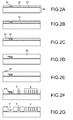
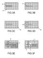
- FIGS. 2A - 2G and 3A - 3F A first method will be described in connection with FIGS. 2A - 2G and 3A - 3F.
- This first method uses a semiconductor epitaxy (here: Silicon, the SiGe is another example), which makes it possible to produce the resonant part in a first, low thickness, then the seismic mass and the hinge in a second thickness, epitaxial on the first thickness and greater than this first thickness.
- a semiconductor epitaxy here: Silicon, the SiGe is another example
- An SOI substrate 20 is first selected (Figure 2A). For example, it comprises a layer 22 of Si 1 ⁇ m thick for a layer 24 of SiO 2 oxide 0.4 ⁇ m thick.
- the etching is stopped on the layer 24 of SiO 2 .
- a layer (not shown) of SiO 2 for example of thickness 2 ⁇ m, is then deposited, followed by a planarization with a stop on layer 22 of Si, then with a deposit 32 of SiO 2 , for example about 0.4 ⁇ m thick ( Figure 2B).
- FIGS. 2C and 3B lithography by etching, in layer 32 of SiO 2 , of a protection 34 above the resonator, with overflow at the level of the excitation / detection electrode.
- Silicon epitaxy 35 is then carried out (FIGS. 2D and 3C) on the initial semiconductor surface layer 22, for example to a thickness of approximately 3 ⁇ m, greater than the thickness of layer 32.
- the device is finally released by HF etching (wet or vapor) of the layer 24 (FIGS. 2G and 3F).
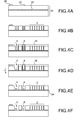
- a second method according to the invention implements a thinning of the resonator 4 and the hinge 6 by etching (FIGS. 4A-4F and 5A-5E).
- An SOI substrate 20 is first selected ( Figure 4A). For example, it comprises a layer 22 of Si of 4 microns thickness for oxide layer 24 of SiO 2 of 0.4 .mu.m thick.
- a Ti / Ni / Au metal deposit and a litho-etching are then made to form contacts 36 (FIGS. 4A and 5A).
- lithography is carried out (FIGS. 4C and 5C), which makes it possible to open the resonator 4, with overflow at the excitation electrode / detection and opening on the hinge 6.
- the device is released by HF etching (wet or vapor) of the layer 24 (FIGS. 4F and 5E).
- the hinge and resonant zones have identical thicknesses because they are etched in depth, along the z axis, during the same step, whereas the patterns of the seismic mass zone are not engraved in this direction.
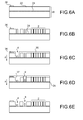
- a third method according to the invention is a variant of the second embodiment, with, in addition, a differential thinning of the resonator 4 and the hinge 6 (or of another mechanical part).
- a SOI substrate 20 is first of all selected ( Figure 6A). For example, it comprises a layer 22 of Si of 4 microns thickness for oxide layer 24 of SiO 2 of 0.4 .mu.m thick.
- a Ti / Ni / Au metal deposit and a litho-etching are then made to form contacts 36 (FIGS. 6A and 7A).
- This step therefore makes it possible to etch the patterns of the seismic mass zone, the resonator zone and the hinge zone.
- the patterns of these last two zones will then be able to be engraved in depth, along the z axis (FIGS. 6C and 6D), but separately to be able to control their relative final thickness.
- an opening of the resonator is produced by lithography, with overflow at the level of the excitation / detection electrode.
- the resonator is etched (RIE or DRIE) along the z axis and then removed from the resin 35.
- FIG. 6D after another deposit of resin 37, a lithographic opening is made at the hinge 6.
- a DRIE etching is carried out along the z axis, but of the hinge 6, then at a removal of the resin 37.
- the device is released by HF etching (wet or vapor) of the layer 24 (FIGS. 6E and 7E).
- the hinge and resonant zones have different thicknesses from one another, and different from the thickness of the seismic zone, because they are etched in depth, along the z axis, during different stages, while the grounds of the seismic mass zone are not etched in this direction.
- the first embodiment although a little more complex (it implements additional steps of planarization and epitaxy), makes it possible to optimize the electrical sensitivity of the electromechanical resonator (optimization of the signal / noise ratio by increasing the capacitances helpful).
- the air gap between the resonator and the excitation / detection electrodes is made directly in a very thin part of silicon. Since the etching of the air gap is done with a thin thickness, a high machining resolution can be achieved.
- resonators and gaps are made on a thick silicon, limiting the fineness of the machining, before being thinned.
- the invention uses zones of different thicknesses in a sensor.
- a sensor according to the invention can be produced by machining silicon or a semiconductor material in the 3 dimensions.
- a resonator according to the invention obtained by 3D machining in a semiconductor material, is particularly well suited for a resonator detection gyro.
- the principle of such a gyrometer is indicated in the document FR-2,874,257 , which is also shown diagrammatically in FIG. 8. It comprises a support, not shown, and two seismic masses 120, 120 'which are movable in the plane (X, Y) of the support, and in particular which can vibrate. These two masses are coupled by connecting means, also moving relative to the support.
- two link arms 140, 140 ' here parallel, are connected to the moving masses via means 160, 160' having sufficient flexibility to allow the relative movements of the two masses 120, 120 'relative to each other.
- the link arms 140, 140 'and the flexible means, or bending arm, 160, 160' form a rectangular frame; the flexible means 160, 160 'may for example be bending springs or an attachment tongue.
- Means are provided to put the masses 120, 120 'in vibration in the plane (X, Y) of the support, for example excitation combs 180, 180' interlocking in one or both sides of each mobile mass 120 , 120 '.
- the masses 120, 120 ' are excited, preferably at resonance or in the vicinity of the resonance, by means of electrostatic forces applied via the inter-digit comb structures 180, 180' together.
- masses 120, 120 'and connecting means 140, 140', 160, 160 'thus form a first resonator
- the resonance operation makes it possible to obtain a high amplitude of displacement, and a large quality factor, thereby increasing the sensitivity of the gyrometer.
- the vibration of the masses 120, 120 ' is in phase opposition, that is to say that their movements are in the opposite direction at each instant: the distance separating the two masses 120, 120' is variable, this variation being tolerated by the flexible means 160, 160 '. This allows detection by second resonators.
- the rotational speed ⁇ about the Z axis is then deduced from the measured frequency displacement.
- the resonator 220 is excited and controlled preferably on its resonance peak or in its vicinity; a digital electronic system makes it possible to easily go back to the resonant frequency at any moment.
- the resonator 220 may for example be in the form of a vibrating beam as shown diagrammatically in FIG. 8, one end of which is connected to the connecting arm 140 and the other end is anchored to the substrate by any known means 240.
- the resonator 220 is excited capacitively resonance by fixed electrodes which are also used for detection. It is also possible to have a detection electrode 260 that is dissociated from the excitation electrode 280.
- Electromagnetic excitation is also possible, as can detection by piezoelectric gage.
- each arm 140, 140 ' is located a torsion axis 300, 300' intended to transform the forces of Coriolis acting at the masses 120, 120 in a pair of forces around this torsion axis 300, 300 ', by a lever effect which makes it possible to exert the greatest possible stress on the resonator.
- Each of the torsion axes is thus attached at one end to the support by an anchor 320, 320 'and at the other end to the connecting arm 140, 140', 160, 160 ', towards the center of the structure 200 to limit the temperature drifts of the gyrometer.
- FIGS. 4A-4D of the document FR-2874257 for example two resonators on one and the same link arm 140 (FIG. 4A), or located on the same side of an axis of the mobile device defined by the torsion axes (FIG. 4B), or else with tuning fork type resonators (FIG. FIG. 4C), or again with resonators arranged as in FIG. 4D of this same document.
- FIGS. 4A-4D of the document FR-2874257 for example two resonators on one and the same link arm 140 (FIG. 4A), or located on the same side of an axis of the mobile device defined by the torsion axes (FIG. 4B), or else with tuning fork type resonators (FIG. FIG. 4C), or again with resonators arranged as in FIG. 4D of this same document.
- the invention makes it possible to produce one or more resonators with a thickness or section smaller than that of the seismic mass or masses.
- the invention makes it possible to have inertial sensors (accelerometers or gyrometers) of very good performance (sensitivity) for very small dimensions.
Landscapes
- Physics & Mathematics (AREA)
- General Physics & Mathematics (AREA)
- Engineering & Computer Science (AREA)
- Radar, Positioning & Navigation (AREA)
- Remote Sensing (AREA)
- Manufacturing & Machinery (AREA)
- Gyroscopes (AREA)
- Pressure Sensors (AREA)
- Micromachines (AREA)
- Diaphragms For Electromechanical Transducers (AREA)
Applications Claiming Priority (1)
| Application Number | Priority Date | Filing Date | Title |
|---|---|---|---|
| FR0651053A FR2898884B1 (fr) | 2006-03-27 | 2006-03-27 | Micro-capteur inertiel resonant a epaisseur variable realise en technologies de surface |
Publications (2)
| Publication Number | Publication Date |
|---|---|
| EP1840582A1 true EP1840582A1 (de) | 2007-10-03 |
| EP1840582B1 EP1840582B1 (de) | 2009-12-09 |
Family
ID=37429311
Family Applications (1)
| Application Number | Title | Priority Date | Filing Date |
|---|---|---|---|
| EP07104737A Active EP1840582B1 (de) | 2006-03-27 | 2007-03-23 | Resonanter Trägheitsmikrosensor variabler Dicke, der im Bereich der Oberflächentechnologien eingesetzt wird |
Country Status (6)
| Country | Link |
|---|---|
| US (1) | US8783107B2 (de) |
| EP (1) | EP1840582B1 (de) |
| JP (1) | JP5562517B2 (de) |
| AT (1) | ATE451621T1 (de) |
| DE (1) | DE602007003625D1 (de) |
| FR (1) | FR2898884B1 (de) |
Cited By (10)
| Publication number | Priority date | Publication date | Assignee | Title |
|---|---|---|---|---|
| WO2009083326A1 (de) * | 2007-12-27 | 2009-07-09 | Robert Bosch Gmbh | Verfahren zur steuerung des energieverbrauchs elektrischer und/oder elektronischer komponenten und vorrichtung |
| WO2010006122A1 (en) * | 2008-07-09 | 2010-01-14 | The Charles Stark Draper Laboratory, Inc. | High-performance sensors and methods for forming the same |
| EP2211143A1 (de) * | 2009-01-23 | 2010-07-28 | Commissariat à l'Énergie Atomique et aux Énergies Alternatives | Planarer mikromechanischer Kreisel mit Messung ausserhalb der Ebene mittels Dehnungsmesser |
| EP2211185A1 (de) * | 2009-01-23 | 2010-07-28 | Commissariat à l'Énergie Atomique et aux Énergies Alternatives | Trägheitssensor oder Resonanzsensor in der Oberflächentechnologie zur Erkennung von Abweichungen mit Hilfe eines Dehnungsmessers |
| US8616059B2 (en) | 2010-03-15 | 2013-12-31 | Commissariat à l'énergie atomique et aux énergies alternatives | Force sensor with reduced noise |
| EP2711696A1 (de) | 2012-09-19 | 2014-03-26 | Commissariat à l'Énergie Atomique et aux Énergies Alternatives | Wärmflusssensor mit Schwingelement und Gas-Sensor mit wenigstens einem solchen Wärmflusssensor |
| WO2016075098A1 (fr) | 2014-11-10 | 2016-05-19 | Tronic's Microsystems | Procede de fabrication d'un dispositif electromecanique et dispositif correspondant |
| WO2017098101A1 (fr) | 2015-12-11 | 2017-06-15 | Tronic's Microsystems | Procede de fabrication d'un dispositif micro electromecanique et dispositif correspondant |
| US9709536B2 (en) | 2012-09-19 | 2017-07-18 | Commissariat à l'énergie atomique et aux énergies alternatives | Thermal flow sensor, gas sensor comprising at least one such sensor and Pirani gauge comprising at least one such sensor |
| US9746384B2 (en) | 2012-09-19 | 2017-08-29 | Commissariat à l'énergie atomique et aux énergies alternatives | Heat flux sensor with increased resolution |
Families Citing this family (30)
| Publication number | Priority date | Publication date | Assignee | Title |
|---|---|---|---|---|
| JP2008092230A (ja) * | 2006-09-29 | 2008-04-17 | Toshiba Corp | 放送受信装置及び放送受信装置のデコード方法 |
| FR2924422B1 (fr) * | 2007-11-30 | 2009-12-25 | Commissariat Energie Atomique | Dispositif a detection par jauge de contrainte piezoresistive suspendue comportant une cellule d'amplification de contrainte. |
| DE102007060942A1 (de) * | 2007-12-18 | 2009-06-25 | Robert Bosch Gmbh | Drehratensensor und Verfahren zum Betrieb eines Drehratensensors |
| US8945912B2 (en) | 2008-09-29 | 2015-02-03 | The Board Of Trustees Of The University Of Illinois | DNA sequencing and amplification systems using nanoscale field effect sensor arrays |
| JP4858547B2 (ja) * | 2009-01-09 | 2012-01-18 | 株式会社デンソー | 半導体装置およびその製造方法 |
| FR2941534B1 (fr) | 2009-01-26 | 2011-12-23 | Commissariat Energie Atomique | Capteur de champ magnetique a jauge de contrainte suspendue |
| FR2951826B1 (fr) * | 2009-10-23 | 2012-06-15 | Commissariat Energie Atomique | Capteur a detection piezoresistive dans le plan |
| FR2954505B1 (fr) * | 2009-12-22 | 2012-08-03 | Commissariat Energie Atomique | Structure micromecanique comportant une partie mobile presentant des butees pour des deplacements hors plan de la structure et son procede de realisation |
| FR2958030B1 (fr) * | 2010-03-23 | 2012-04-20 | Sagem Defense Securite | Procede et dispositif de mesure angulaire avec compensation de non linearites |
| GB201009062D0 (en) * | 2010-05-28 | 2010-07-14 | Cambridge Entpr Ltd | MEMS inertial sensor and method of inertial sensing |
| WO2011163058A2 (en) * | 2010-06-21 | 2011-12-29 | The Board Of Trustees Of The University Of Illinois | Cell mass measurement and apparatus |
| FR2963192B1 (fr) | 2010-07-22 | 2013-07-19 | Commissariat Energie Atomique | Générateur d'impulsions de pression de type mems |
| FR2963099B1 (fr) | 2010-07-22 | 2013-10-04 | Commissariat Energie Atomique | Capteur de pression dynamique mems, en particulier pour des applications a la realisation de microphones |
| FR2965349B1 (fr) | 2010-09-23 | 2017-01-20 | Commissariat Energie Atomique | Bolometre a detection frequentielle |
| US8779534B2 (en) | 2010-11-04 | 2014-07-15 | Meggitt (Orange County), Inc. | Low-G MEMS acceleration switch |
| EP2762893B1 (de) * | 2011-09-30 | 2016-06-15 | Microinfinity, Inc. | Resonanter mems-beschleunigungsmesser |
| TWI607956B (zh) * | 2012-01-12 | 2017-12-11 | 村田電子公司 | 振動容限的加速感測器結構 |
| JP5874609B2 (ja) * | 2012-03-27 | 2016-03-02 | 株式会社デンソー | 半導体装置およびその製造方法 |
| FR3017463B1 (fr) | 2014-02-13 | 2020-11-13 | Commissariat Energie Atomique | Capteur de concentration de gaz a structure suspendue |
| JP6044607B2 (ja) * | 2014-08-28 | 2016-12-14 | 横河電機株式会社 | 振動式センサ装置 |
| US9903718B2 (en) * | 2015-05-28 | 2018-02-27 | Invensense, Inc. | MEMS device mechanical amplitude control |
| US10634499B2 (en) | 2015-06-11 | 2020-04-28 | Georgia Tech Research Corporation | MEMS inertial measurement apparatus having slanted electrodes for quadrature tuning |
| WO2017056920A1 (ja) * | 2015-09-30 | 2017-04-06 | 株式会社デンソー | 半導体装置の製造方法 |
| WO2017075413A1 (en) | 2015-10-28 | 2017-05-04 | Georgia Tech Research Corporation | Comb-driven substrate decoupled annulus pitch/roll baw gyroscope with slanted quadrature tuning electrode |
| WO2018057071A1 (en) | 2016-06-07 | 2018-03-29 | Georgia Tech Research Corporation | Pitch/roll annulus gyroscope with slanted quadrature tuning electrodes and related fabrication methods |
| GB2561889B (en) | 2017-04-27 | 2022-10-12 | Cambridge Entpr Ltd | High performance micro-electro-mechanical systems accelerometer with electrostatic control of proof mass |
| US10895457B2 (en) | 2018-03-08 | 2021-01-19 | Analog Devices, Inc. | Differential z-axis resonant accelerometry |
| RU2692122C1 (ru) * | 2018-11-23 | 2019-06-21 | Федеральное государственное автономное образовательное учреждение высшего образования "Национальный исследовательский университет "Московский институт электронной техники" | Твердотельный датчик линейных ускорений |
| US11493531B2 (en) * | 2019-11-07 | 2022-11-08 | Honeywell International Inc. | Resonator electrode configuration to avoid capacitive feedthrough for vibrating beam accelerometers |
| JP2024011323A (ja) * | 2022-07-14 | 2024-01-25 | 株式会社東芝 | センサ及び電子装置 |
Citations (3)
| Publication number | Priority date | Publication date | Assignee | Title |
|---|---|---|---|---|
| FR2763694A1 (fr) * | 1997-05-23 | 1998-11-27 | Sextant Avionique | Micro-accelerometre a resonateur capacitif |
| FR2784752A1 (fr) * | 1998-10-20 | 2000-04-21 | Onera (Off Nat Aerospatiale) | Accelerometre miniature monolithique |
| FR2874257A1 (fr) * | 2004-08-13 | 2006-02-17 | Commissariat Energie Atomique | Micro gyrometre a detection frenquentielle |
Family Cites Families (16)
| Publication number | Priority date | Publication date | Assignee | Title |
|---|---|---|---|---|
| FR2627592B1 (fr) * | 1988-02-22 | 1990-07-27 | Sagem | Accelerometre pendulaire non asservi a poutre resonante |
| FR2685964B1 (fr) | 1992-01-06 | 1996-06-07 | Onera (Off Nat Aerospatiale) | Capteur accelerometrique miniature a lames vibrant en flexion. |
| JP3161057B2 (ja) | 1992-06-26 | 2001-04-25 | 株式会社村田製作所 | 振動型センサの振動子 |
| JPH1026532A (ja) * | 1996-07-12 | 1998-01-27 | Mitsubishi Electric Corp | 半導体角速度検出装置 |
| JPH10122867A (ja) | 1996-08-26 | 1998-05-15 | Fuji Electric Co Ltd | マイクロジャイロ |
| US5996411A (en) * | 1996-11-25 | 1999-12-07 | Alliedsignal Inc. | Vibrating beam accelerometer and method for manufacturing the same |
| DE19649715C2 (de) * | 1996-11-30 | 2001-07-12 | Telefunken Microelectron | Anordnung zur Messung von Beschleunigungen |
| US6250158B1 (en) * | 1997-05-09 | 2001-06-26 | Litton Systems, Inc. | Monolithic vibrating beam angular velocity sensor |
| JPH11214706A (ja) | 1998-01-27 | 1999-08-06 | Toyota Motor Corp | 半導体センサおよびその製造方法 |
| DE19812773C2 (de) * | 1998-03-24 | 2002-11-14 | Conti Temic Microelectronic | Mikrosensor mit einer Resonatorstruktur |
| JP2000146592A (ja) | 1998-11-16 | 2000-05-26 | Toyota Central Res & Dev Lab Inc | 振動式検出器 |
| WO2005012923A1 (ja) * | 2003-08-04 | 2005-02-10 | Murata Manufacturing Co., Ltd. | 加速度センサ |
| JP4556454B2 (ja) * | 2004-03-15 | 2010-10-06 | パナソニック電工株式会社 | 半導体装置の製造方法 |
| JP4847686B2 (ja) | 2004-05-26 | 2011-12-28 | パナソニック電工株式会社 | 半導体加速度センサ |
| FR2880127B1 (fr) * | 2004-12-29 | 2007-03-02 | Commissariat Energie Atomique | Accelerometre micro-usine a peignes capacitifs |
| FR2880128B1 (fr) * | 2004-12-29 | 2007-02-02 | Commissariat Energie Atomique | Accelerometre micro-usine a peignes capacitifs |
-
2006
- 2006-03-27 FR FR0651053A patent/FR2898884B1/fr not_active Expired - Fee Related
-
2007
- 2007-03-15 US US11/724,795 patent/US8783107B2/en active Active
- 2007-03-23 EP EP07104737A patent/EP1840582B1/de active Active
- 2007-03-23 AT AT07104737T patent/ATE451621T1/de not_active IP Right Cessation
- 2007-03-23 DE DE602007003625T patent/DE602007003625D1/de active Active
- 2007-03-27 JP JP2007080397A patent/JP5562517B2/ja active Active
Patent Citations (3)
| Publication number | Priority date | Publication date | Assignee | Title |
|---|---|---|---|---|
| FR2763694A1 (fr) * | 1997-05-23 | 1998-11-27 | Sextant Avionique | Micro-accelerometre a resonateur capacitif |
| FR2784752A1 (fr) * | 1998-10-20 | 2000-04-21 | Onera (Off Nat Aerospatiale) | Accelerometre miniature monolithique |
| FR2874257A1 (fr) * | 2004-08-13 | 2006-02-17 | Commissariat Energie Atomique | Micro gyrometre a detection frenquentielle |
Non-Patent Citations (2)
| Title |
|---|
| AIKELE M ET AL: "Resonant accelerometer with self-test", SENSORS AND ACTUATORS A, ELSEVIER SEQUOIA S.A., LAUSANNE, CH, vol. 92, no. 1-3, 1 August 2001 (2001-08-01), pages 161 - 167, XP004274041, ISSN: 0924-4247 * |
| CHRISTOFER HIEROLD ET AL: "From micro- to nanosystems: mechanical sensors go nano", JOURNAL OF MICROMECHANICS & MICROENGINEERING, INSTITUTE OF PHYSICS PUBLISHING, BRISTOL, GB, vol. 14, no. 9, 1 September 2004 (2004-09-01), pages S1 - S11, XP020069754, ISSN: 0960-1317 * |
Cited By (16)
| Publication number | Priority date | Publication date | Assignee | Title |
|---|---|---|---|---|
| WO2009083326A1 (de) * | 2007-12-27 | 2009-07-09 | Robert Bosch Gmbh | Verfahren zur steuerung des energieverbrauchs elektrischer und/oder elektronischer komponenten und vorrichtung |
| US8187902B2 (en) | 2008-07-09 | 2012-05-29 | The Charles Stark Draper Laboratory, Inc. | High performance sensors and methods for forming the same |
| WO2010006122A1 (en) * | 2008-07-09 | 2010-01-14 | The Charles Stark Draper Laboratory, Inc. | High-performance sensors and methods for forming the same |
| US8375788B2 (en) | 2009-01-23 | 2013-02-19 | Commissariat A L'energie Atomique | Gyrometer in surface technology, with out-of-plane detection by strain gauge |
| FR2941533A1 (fr) * | 2009-01-23 | 2010-07-30 | Commissariat Energie Atomique | Capteur inertiel ou resonnant en technologie de surface, a detection hors plan par jauge de contrainte. |
| FR2941525A1 (fr) * | 2009-01-23 | 2010-07-30 | Commissariat Energie Atomique | Gyrometre en technologie de surface, a detection hors plan par jauge de contrainte. |
| EP2211185A1 (de) * | 2009-01-23 | 2010-07-28 | Commissariat à l'Énergie Atomique et aux Énergies Alternatives | Trägheitssensor oder Resonanzsensor in der Oberflächentechnologie zur Erkennung von Abweichungen mit Hilfe eines Dehnungsmessers |
| US8371166B2 (en) | 2009-01-23 | 2013-02-12 | Commissariat A L'energie Atomique | Inertial or resonating sensor in surface technology, with out of plane detection by strain gauge |
| EP2211143A1 (de) * | 2009-01-23 | 2010-07-28 | Commissariat à l'Énergie Atomique et aux Énergies Alternatives | Planarer mikromechanischer Kreisel mit Messung ausserhalb der Ebene mittels Dehnungsmesser |
| US8616059B2 (en) | 2010-03-15 | 2013-12-31 | Commissariat à l'énergie atomique et aux énergies alternatives | Force sensor with reduced noise |
| EP2711696A1 (de) | 2012-09-19 | 2014-03-26 | Commissariat à l'Énergie Atomique et aux Énergies Alternatives | Wärmflusssensor mit Schwingelement und Gas-Sensor mit wenigstens einem solchen Wärmflusssensor |
| US9599495B2 (en) | 2012-09-19 | 2017-03-21 | Commissariat à l'énergie atomique et aux énergies alternatives | Thermal flow sensor with vibrating element and gas sensor comprising at least one such sensor |
| US9709536B2 (en) | 2012-09-19 | 2017-07-18 | Commissariat à l'énergie atomique et aux énergies alternatives | Thermal flow sensor, gas sensor comprising at least one such sensor and Pirani gauge comprising at least one such sensor |
| US9746384B2 (en) | 2012-09-19 | 2017-08-29 | Commissariat à l'énergie atomique et aux énergies alternatives | Heat flux sensor with increased resolution |
| WO2016075098A1 (fr) | 2014-11-10 | 2016-05-19 | Tronic's Microsystems | Procede de fabrication d'un dispositif electromecanique et dispositif correspondant |
| WO2017098101A1 (fr) | 2015-12-11 | 2017-06-15 | Tronic's Microsystems | Procede de fabrication d'un dispositif micro electromecanique et dispositif correspondant |
Also Published As
| Publication number | Publication date |
|---|---|
| FR2898884B1 (fr) | 2008-05-02 |
| JP5562517B2 (ja) | 2014-07-30 |
| US20070222011A1 (en) | 2007-09-27 |
| FR2898884A1 (fr) | 2007-09-28 |
| DE602007003625D1 (de) | 2010-01-21 |
| ATE451621T1 (de) | 2009-12-15 |
| JP2007316056A (ja) | 2007-12-06 |
| EP1840582B1 (de) | 2009-12-09 |
| US8783107B2 (en) | 2014-07-22 |
Similar Documents
| Publication | Publication Date | Title |
|---|---|---|
| EP1840582B1 (de) | Resonanter Trägheitsmikrosensor variabler Dicke, der im Bereich der Oberflächentechnologien eingesetzt wird | |
| EP2211143B1 (de) | Planarer mikromechanischer Kreisel mit Messung ausserhalb der Ebene mittels Dehnungsmesser | |
| EP2211185B1 (de) | Trägheitssensor oder Resonanzsensor in der Oberflächentechnologie zur Erkennung von Abweichungen mit Hilfe eines Dehnungsmessers | |
| EP2008965B1 (de) | Resonanzvorrichtung mit piezoelektrischer Erfassung für den Einsatz in Oberflächentechnologien | |
| EP2367015B1 (de) | Rauscharmer kraftsensor | |
| EP2541222B1 (de) | Druckmessgerät mit optimierter Emfpindlichkeit | |
| EP2343556B1 (de) | Mikromechanische Struktur, die einen mobilen Teil mit Anschlägen für Bewegungen außerhalb der Planebene der Struktur umfasst, und ihr Herstellungsverfahren | |
| EP1626282B1 (de) | Mikrokreisel mit Frequenzdetektion | |
| EP2617129B1 (de) | Vorrichtung mit freihängendem träger und piezoresistive vorrichtung zur verlagerungserkennung | |
| EP2065713B1 (de) | Erfassungsvorrichtung mittels aufgehängtem Dehnungsmesser mit piezoelektrischem Widerstand, der eine Dehnungsverstärkungszelle umfasst | |
| EP2617130B1 (de) | Resonanter piezoresistiver detektor mit einem an das trägerelement des detektors elastisch angeschlossenen resonator und verfahren zur herstellung dieses detektors | |
| EP3599469B1 (de) | Beschleunigungssensor mit dehnungsmessstreifen mit verbesserter präzision | |
| EP2520900B1 (de) | Gyroskop mit reduzierter parasitärer Kapazität | |
| WO2012085456A2 (fr) | Structure planaire pour gyromètre tri-axe | |
| EP2616386B1 (de) | In der ebene betätigte resonanzvorrichtung und verfahren zur herstellung der vorrichtung | |
| FR3059312A1 (fr) | Procede de realisation d’un dispositif electromecanique | |
| EP2949621B1 (de) | Kapazitive mikro- und/ oder nanoelektronische Vorrichtung mit erhöhter Kompaktheit | |
| EP1353185B1 (de) | Ineritalsensor mit integrierter Temperatursonde | |
| FR2973608A1 (fr) | Procede d'ajustement de la frequence de resonance d'un element vibrant micro-usine |
Legal Events
| Date | Code | Title | Description |
|---|---|---|---|
| PUAI | Public reference made under article 153(3) epc to a published international application that has entered the european phase |
Free format text: ORIGINAL CODE: 0009012 |
|
| AK | Designated contracting states |
Kind code of ref document: A1 Designated state(s): AT BE BG CH CY CZ DE DK EE ES FI FR GB GR HU IE IS IT LI LT LU LV MC MT NL PL PT RO SE SI SK TR |
|
| AX | Request for extension of the european patent |
Extension state: AL BA HR MK YU |
|
| 17P | Request for examination filed |
Effective date: 20080402 |
|
| AKX | Designation fees paid |
Designated state(s): AT BE BG CH CY CZ DE DK EE ES FI FR GB GR HU IE IS IT LI LT LU LV MC MT NL PL PT RO SE SI SK TR |
|
| GRAP | Despatch of communication of intention to grant a patent |
Free format text: ORIGINAL CODE: EPIDOSNIGR1 |
|
| GRAS | Grant fee paid |
Free format text: ORIGINAL CODE: EPIDOSNIGR3 |
|
| GRAA | (expected) grant |
Free format text: ORIGINAL CODE: 0009210 |
|
| AK | Designated contracting states |
Kind code of ref document: B1 Designated state(s): AT BE BG CH CY CZ DE DK EE ES FI FR GB GR HU IE IS IT LI LT LU LV MC MT NL PL PT RO SE SI SK TR |
|
| REG | Reference to a national code |
Ref country code: GB Ref legal event code: FG4D Free format text: NOT ENGLISH |
|
| REG | Reference to a national code |
Ref country code: CH Ref legal event code: EP |
|
| REG | Reference to a national code |
Ref country code: IE Ref legal event code: FG4D |
|
| REF | Corresponds to: |
Ref document number: 602007003625 Country of ref document: DE Date of ref document: 20100121 Kind code of ref document: P |
|
| REG | Reference to a national code |
Ref country code: NL Ref legal event code: VDEP Effective date: 20091209 |
|
| PG25 | Lapsed in a contracting state [announced via postgrant information from national office to epo] |
Ref country code: FI Free format text: LAPSE BECAUSE OF FAILURE TO SUBMIT A TRANSLATION OF THE DESCRIPTION OR TO PAY THE FEE WITHIN THE PRESCRIBED TIME-LIMIT Effective date: 20091209 Ref country code: LT Free format text: LAPSE BECAUSE OF FAILURE TO SUBMIT A TRANSLATION OF THE DESCRIPTION OR TO PAY THE FEE WITHIN THE PRESCRIBED TIME-LIMIT Effective date: 20091209 Ref country code: SE Free format text: LAPSE BECAUSE OF FAILURE TO SUBMIT A TRANSLATION OF THE DESCRIPTION OR TO PAY THE FEE WITHIN THE PRESCRIBED TIME-LIMIT Effective date: 20091209 |
|
| LTIE | Lt: invalidation of european patent or patent extension |
Effective date: 20091209 |
|
| PG25 | Lapsed in a contracting state [announced via postgrant information from national office to epo] |
Ref country code: PL Free format text: LAPSE BECAUSE OF FAILURE TO SUBMIT A TRANSLATION OF THE DESCRIPTION OR TO PAY THE FEE WITHIN THE PRESCRIBED TIME-LIMIT Effective date: 20091209 Ref country code: LV Free format text: LAPSE BECAUSE OF FAILURE TO SUBMIT A TRANSLATION OF THE DESCRIPTION OR TO PAY THE FEE WITHIN THE PRESCRIBED TIME-LIMIT Effective date: 20091209 Ref country code: SI Free format text: LAPSE BECAUSE OF FAILURE TO SUBMIT A TRANSLATION OF THE DESCRIPTION OR TO PAY THE FEE WITHIN THE PRESCRIBED TIME-LIMIT Effective date: 20091209 |
|
| PG25 | Lapsed in a contracting state [announced via postgrant information from national office to epo] |
Ref country code: AT Free format text: LAPSE BECAUSE OF FAILURE TO SUBMIT A TRANSLATION OF THE DESCRIPTION OR TO PAY THE FEE WITHIN THE PRESCRIBED TIME-LIMIT Effective date: 20091209 |
|
| REG | Reference to a national code |
Ref country code: IE Ref legal event code: FD4D |
|
| PG25 | Lapsed in a contracting state [announced via postgrant information from national office to epo] |
Ref country code: EE Free format text: LAPSE BECAUSE OF FAILURE TO SUBMIT A TRANSLATION OF THE DESCRIPTION OR TO PAY THE FEE WITHIN THE PRESCRIBED TIME-LIMIT Effective date: 20091209 Ref country code: IE Free format text: LAPSE BECAUSE OF FAILURE TO SUBMIT A TRANSLATION OF THE DESCRIPTION OR TO PAY THE FEE WITHIN THE PRESCRIBED TIME-LIMIT Effective date: 20091209 Ref country code: RO Free format text: LAPSE BECAUSE OF FAILURE TO SUBMIT A TRANSLATION OF THE DESCRIPTION OR TO PAY THE FEE WITHIN THE PRESCRIBED TIME-LIMIT Effective date: 20091209 Ref country code: NL Free format text: LAPSE BECAUSE OF FAILURE TO SUBMIT A TRANSLATION OF THE DESCRIPTION OR TO PAY THE FEE WITHIN THE PRESCRIBED TIME-LIMIT Effective date: 20091209 Ref country code: PT Free format text: LAPSE BECAUSE OF FAILURE TO SUBMIT A TRANSLATION OF THE DESCRIPTION OR TO PAY THE FEE WITHIN THE PRESCRIBED TIME-LIMIT Effective date: 20100409 Ref country code: IS Free format text: LAPSE BECAUSE OF FAILURE TO SUBMIT A TRANSLATION OF THE DESCRIPTION OR TO PAY THE FEE WITHIN THE PRESCRIBED TIME-LIMIT Effective date: 20100409 Ref country code: ES Free format text: LAPSE BECAUSE OF FAILURE TO SUBMIT A TRANSLATION OF THE DESCRIPTION OR TO PAY THE FEE WITHIN THE PRESCRIBED TIME-LIMIT Effective date: 20100320 Ref country code: BG Free format text: LAPSE BECAUSE OF FAILURE TO SUBMIT A TRANSLATION OF THE DESCRIPTION OR TO PAY THE FEE WITHIN THE PRESCRIBED TIME-LIMIT Effective date: 20100309 |
|
| PG25 | Lapsed in a contracting state [announced via postgrant information from national office to epo] |
Ref country code: CZ Free format text: LAPSE BECAUSE OF FAILURE TO SUBMIT A TRANSLATION OF THE DESCRIPTION OR TO PAY THE FEE WITHIN THE PRESCRIBED TIME-LIMIT Effective date: 20091209 Ref country code: SK Free format text: LAPSE BECAUSE OF FAILURE TO SUBMIT A TRANSLATION OF THE DESCRIPTION OR TO PAY THE FEE WITHIN THE PRESCRIBED TIME-LIMIT Effective date: 20091209 |
|
| BERE | Be: lapsed |
Owner name: COMMISSARIAT A L'ENERGIE ATOMIQUE Effective date: 20100331 |
|
| PLBE | No opposition filed within time limit |
Free format text: ORIGINAL CODE: 0009261 |
|
| STAA | Information on the status of an ep patent application or granted ep patent |
Free format text: STATUS: NO OPPOSITION FILED WITHIN TIME LIMIT |
|
| PG25 | Lapsed in a contracting state [announced via postgrant information from national office to epo] |
Ref country code: CY Free format text: LAPSE BECAUSE OF FAILURE TO SUBMIT A TRANSLATION OF THE DESCRIPTION OR TO PAY THE FEE WITHIN THE PRESCRIBED TIME-LIMIT Effective date: 20091209 Ref country code: GR Free format text: LAPSE BECAUSE OF FAILURE TO SUBMIT A TRANSLATION OF THE DESCRIPTION OR TO PAY THE FEE WITHIN THE PRESCRIBED TIME-LIMIT Effective date: 20100310 Ref country code: MC Free format text: LAPSE BECAUSE OF NON-PAYMENT OF DUE FEES Effective date: 20100331 |
|
| 26N | No opposition filed |
Effective date: 20100910 |
|
| PG25 | Lapsed in a contracting state [announced via postgrant information from national office to epo] |
Ref country code: DK Free format text: LAPSE BECAUSE OF FAILURE TO SUBMIT A TRANSLATION OF THE DESCRIPTION OR TO PAY THE FEE WITHIN THE PRESCRIBED TIME-LIMIT Effective date: 20091209 |
|
| PG25 | Lapsed in a contracting state [announced via postgrant information from national office to epo] |
Ref country code: BE Free format text: LAPSE BECAUSE OF NON-PAYMENT OF DUE FEES Effective date: 20100331 |
|
| PG25 | Lapsed in a contracting state [announced via postgrant information from national office to epo] |
Ref country code: MT Free format text: LAPSE BECAUSE OF FAILURE TO SUBMIT A TRANSLATION OF THE DESCRIPTION OR TO PAY THE FEE WITHIN THE PRESCRIBED TIME-LIMIT Effective date: 20091209 |
|
| PGRI | Patent reinstated in contracting state [announced from national office to epo] |
Ref country code: IT Effective date: 20110501 |
|
| REG | Reference to a national code |
Ref country code: CH Ref legal event code: PL |
|
| PG25 | Lapsed in a contracting state [announced via postgrant information from national office to epo] |
Ref country code: CH Free format text: LAPSE BECAUSE OF NON-PAYMENT OF DUE FEES Effective date: 20110331 Ref country code: LI Free format text: LAPSE BECAUSE OF NON-PAYMENT OF DUE FEES Effective date: 20110331 |
|
| PG25 | Lapsed in a contracting state [announced via postgrant information from national office to epo] |
Ref country code: HU Free format text: LAPSE BECAUSE OF FAILURE TO SUBMIT A TRANSLATION OF THE DESCRIPTION OR TO PAY THE FEE WITHIN THE PRESCRIBED TIME-LIMIT Effective date: 20100610 Ref country code: LU Free format text: LAPSE BECAUSE OF NON-PAYMENT OF DUE FEES Effective date: 20100323 |
|
| PG25 | Lapsed in a contracting state [announced via postgrant information from national office to epo] |
Ref country code: TR Free format text: LAPSE BECAUSE OF FAILURE TO SUBMIT A TRANSLATION OF THE DESCRIPTION OR TO PAY THE FEE WITHIN THE PRESCRIBED TIME-LIMIT Effective date: 20091209 |
|
| REG | Reference to a national code |
Ref country code: FR Ref legal event code: PLFP Year of fee payment: 10 |
|
| REG | Reference to a national code |
Ref country code: FR Ref legal event code: PLFP Year of fee payment: 11 |
|
| REG | Reference to a national code |
Ref country code: FR Ref legal event code: PLFP Year of fee payment: 12 |
|
| PGFP | Annual fee paid to national office [announced via postgrant information from national office to epo] |
Ref country code: IT Payment date: 20250331 Year of fee payment: 19 |
|
| PGFP | Annual fee paid to national office [announced via postgrant information from national office to epo] |
Ref country code: GB Payment date: 20260324 Year of fee payment: 20 |
|
| PGFP | Annual fee paid to national office [announced via postgrant information from national office to epo] |
Ref country code: DE Payment date: 20260320 Year of fee payment: 20 |
|
| PGFP | Annual fee paid to national office [announced via postgrant information from national office to epo] |
Ref country code: FR Payment date: 20260324 Year of fee payment: 20 |