EP2873308B1 - Circuit imprimé équipé d'un sous-ensemble à haute fréquence émettant des ondes parasites - Google Patents
Circuit imprimé équipé d'un sous-ensemble à haute fréquence émettant des ondes parasites Download PDFInfo
- Publication number
- EP2873308B1 EP2873308B1 EP13729650.5A EP13729650A EP2873308B1 EP 2873308 B1 EP2873308 B1 EP 2873308B1 EP 13729650 A EP13729650 A EP 13729650A EP 2873308 B1 EP2873308 B1 EP 2873308B1
- Authority
- EP
- European Patent Office
- Prior art keywords
- printed circuit
- circuit board
- waveguide
- frequency
- interference waves
- Prior art date
- Legal status (The legal status is an assumption and is not a legal conclusion. Google has not performed a legal analysis and makes no representation as to the accuracy of the status listed.)
- Not-in-force
Links
Images
Classifications
-
- H—ELECTRICITY
- H05—ELECTRIC TECHNIQUES NOT OTHERWISE PROVIDED FOR
- H05K—PRINTED CIRCUITS; CASINGS OR CONSTRUCTIONAL DETAILS OF ELECTRIC APPARATUS; MANUFACTURE OF ASSEMBLAGES OF ELECTRICAL COMPONENTS
- H05K1/00—Printed circuits
- H05K1/02—Details
- H05K1/0213—Electrical arrangements not otherwise provided for
- H05K1/0237—High frequency adaptations
- H05K1/024—Dielectric details, e.g. changing the dielectric material around a transmission line
-
- H—ELECTRICITY
- H05—ELECTRIC TECHNIQUES NOT OTHERWISE PROVIDED FOR
- H05K—PRINTED CIRCUITS; CASINGS OR CONSTRUCTIONAL DETAILS OF ELECTRIC APPARATUS; MANUFACTURE OF ASSEMBLAGES OF ELECTRICAL COMPONENTS
- H05K1/00—Printed circuits
- H05K1/02—Details
- H05K1/0213—Electrical arrangements not otherwise provided for
- H05K1/0216—Reduction of cross-talk, noise or electromagnetic interference
- H05K1/0218—Reduction of cross-talk, noise or electromagnetic interference by printed shielding conductors, ground planes or power plane
- H05K1/0224—Patterned shielding planes, ground planes or power planes
- H05K1/0227—Split or nearly split shielding or ground planes
-
- H—ELECTRICITY
- H05—ELECTRIC TECHNIQUES NOT OTHERWISE PROVIDED FOR
- H05K—PRINTED CIRCUITS; CASINGS OR CONSTRUCTIONAL DETAILS OF ELECTRIC APPARATUS; MANUFACTURE OF ASSEMBLAGES OF ELECTRICAL COMPONENTS
- H05K1/00—Printed circuits
- H05K1/02—Details
- H05K1/0213—Electrical arrangements not otherwise provided for
- H05K1/0216—Reduction of cross-talk, noise or electromagnetic interference
- H05K1/023—Reduction of cross-talk, noise or electromagnetic interference using auxiliary mounted passive components or auxiliary substances
- H05K1/0231—Capacitors or dielectric substances
-
- H—ELECTRICITY
- H05—ELECTRIC TECHNIQUES NOT OTHERWISE PROVIDED FOR
- H05K—PRINTED CIRCUITS; CASINGS OR CONSTRUCTIONAL DETAILS OF ELECTRIC APPARATUS; MANUFACTURE OF ASSEMBLAGES OF ELECTRICAL COMPONENTS
- H05K1/00—Printed circuits
- H05K1/02—Details
- H05K1/0213—Electrical arrangements not otherwise provided for
- H05K1/0216—Reduction of cross-talk, noise or electromagnetic interference
- H05K1/023—Reduction of cross-talk, noise or electromagnetic interference using auxiliary mounted passive components or auxiliary substances
- H05K1/0234—Resistors or by disposing resistive or lossy substances in or near power planes
-
- H—ELECTRICITY
- H05—ELECTRIC TECHNIQUES NOT OTHERWISE PROVIDED FOR
- H05K—PRINTED CIRCUITS; CASINGS OR CONSTRUCTIONAL DETAILS OF ELECTRIC APPARATUS; MANUFACTURE OF ASSEMBLAGES OF ELECTRICAL COMPONENTS
- H05K1/00—Printed circuits
- H05K1/02—Details
- H05K1/0213—Electrical arrangements not otherwise provided for
- H05K1/0237—High frequency adaptations
- H05K1/0243—Printed circuits associated with mounted high frequency components
-
- H—ELECTRICITY
- H01—ELECTRIC ELEMENTS
- H01P—WAVEGUIDES; RESONATORS, LINES, OR OTHER DEVICES OF THE WAVEGUIDE TYPE
- H01P1/00—Auxiliary devices
- H01P1/20—Frequency-selective devices, e.g. filters
- H01P1/201—Filters for transverse electromagnetic waves
- H01P1/2016—Slot line filters; Fin line filters
-
- H—ELECTRICITY
- H01—ELECTRIC ELEMENTS
- H01P—WAVEGUIDES; RESONATORS, LINES, OR OTHER DEVICES OF THE WAVEGUIDE TYPE
- H01P3/00—Waveguides; Transmission lines of the waveguide type
- H01P3/02—Waveguides; Transmission lines of the waveguide type with two longitudinal conductors
- H01P3/023—Fin lines; Slot lines
-
- H—ELECTRICITY
- H05—ELECTRIC TECHNIQUES NOT OTHERWISE PROVIDED FOR
- H05K—PRINTED CIRCUITS; CASINGS OR CONSTRUCTIONAL DETAILS OF ELECTRIC APPARATUS; MANUFACTURE OF ASSEMBLAGES OF ELECTRICAL COMPONENTS
- H05K2201/00—Indexing scheme relating to printed circuits covered by H05K1/00
- H05K2201/01—Dielectrics
- H05K2201/0183—Dielectric layers
- H05K2201/0187—Dielectric layers with regions of different dielectrics in the same layer, e.g. in a printed capacitor for locally changing the dielectric properties
-
- H—ELECTRICITY
- H05—ELECTRIC TECHNIQUES NOT OTHERWISE PROVIDED FOR
- H05K—PRINTED CIRCUITS; CASINGS OR CONSTRUCTIONAL DETAILS OF ELECTRIC APPARATUS; MANUFACTURE OF ASSEMBLAGES OF ELECTRICAL COMPONENTS
- H05K2201/00—Indexing scheme relating to printed circuits covered by H05K1/00
- H05K2201/09—Shape and layout
- H05K2201/09209—Shape and layout details of conductors
- H05K2201/0929—Conductive planes
- H05K2201/09318—Core having one signal plane and one power plane
Definitions
- the invention relates to a printed circuit board with a printed circuit board layer on which a high-frequency assembly, which emits high-frequency electromagnetic interference waves during operation, and at least one further assembly, in particular a high-frequency assembly, are provided.
- high frequency refers to frequencies in the range from 3 MHz to 300 GHz.
- High-frequency assemblies refer to circuits or circuit parts which have at least one circuit component operating at these frequencies.
- level measuring devices that operate with microwaves according to the pulse radar method.
- the latter are used to measure the level of a product located in a container. They have an antenna arranged above the product, via which short microwave pulses of a specified transmission frequency are periodically sent in the direction of the product during measurement operation, and the signal components reflected on the product surface are received after a transit time that depends on the fill level.
- These level measuring devices regularly have a high-frequency module with which the transmission signals are generated and their reflected signal components are prepared and processed for the transit time measurement.
- the high-frequency module has several high-frequency assemblies, such as a transmission circuit for generating the transmission signal, a reception circuit for receiving the reflected signal components and processing circuits for determining the transit time.
- high-frequency assemblies usually emit high-frequency electromagnetic interference waves. Conversely, however, high-frequency assemblies in particular are often very sensitive to high-frequency interference.
- high-frequency electromagnetic interference fields are usually capable of propagation both above the circuit board and within individual circuit board layers of circuit boards.
- a comparatively wide copper conductor track can be applied to a circuit board layer between the adjacent assemblies, which causes a disruption of wave components spreading above the circuit board layer.
- plated-through holes can be provided along the copper conductor track, via which the copper conductor track is conductively connected to a copper layer located under the circuit board layer.
- a section of the circuit board layer located between two plated-through holes acts like a metallic waveguide, the cut-off frequency of which can be set by its dimensioning and the dielectric properties of the circuit board layer.
- interference signals with frequencies below the cut-off frequency cannot propagate in the waveguide.
- Solid metallic webs provide high quality interference suppression.
- they have the disadvantage that they are costly and have to be taken into account with every change in the circuit board layout or, in most cases, also have to be changed in their position.
- the DE 10 2010 061 714 A1 described to place an at least partially metallized cover on a sub-area of the circuit board, which shields the sub-area below from electromagnetic interference fields to which the top of the circuit board is exposed and prevents electromagnetic interference from escaping.
- the interior of the cover can be filled with a conductive foam in which multiple reflections of electromagnetic waves take place, which lead to undirected damping of the interference waves.
- a minimum distance of a quarter wavelength must be maintained between the foam and the adjacent high-frequency lines.
- EP 1 962 377 A1 describes two antennas arranged on a printed circuit board, between which a photonic crystal structure is arranged.
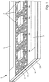
- Fig. 1 and Fig. 2 each show a view of a printed circuit board 1, which has a printed circuit board layer 3 on which a high-frequency assembly 5 - here only shown schematically - emitting high-frequency electromagnetic interference waves during operation and at least one further - here also only shown schematically- module 7, in particular a further high-frequency module , are provided.
- At least one dielectric interferer 9a, 9b is provided between the high-frequency assembly 5 and the further assembly 7, which interferes with the propagation of high-frequency electromagnetic interference waves between the high-frequency assembly 5 and the further assembly 7.
- High-frequency electromagnetic waves are capable of propagation both above the circuit board layer 3 and in the circuit board layer 3.
- the invention comprises a variant with at least one dielectric interferer 9a arranged on an upper side of the circuit board layer 3, which brings about a reduction of electromagnetic waves transmitted above the circuit board layer 3, and a second variant with at least one dielectric interferer 9b arranged in the circuit board layer 3, the hinders the propagation of electromagnetic waves within the circuit board layer 3.
- Fig. 1 shows a preferred embodiment of the first variant.
- the dielectric interferers 9a arranged on the printed circuit board layer 3 are bodies arranged on the printed circuit board layer 3, such as, for example, cubes or cuboids made of a dielectric.
- ⁇ components having a dielectric core e.g. Resistors or capacitors equipped with a dielectric core, used as interferers 9a.
- Electronic components whose core has a high dielectric constant are preferred.
- components are preferably used which can be applied to the circuit board 1 in an assembly process that is to be carried out in any case during the regular assembly of the circuit board 1.
- SMD components soldered onto the conductor track 11.
- plated-through holes P are preferably provided along the conductor track 11, via which the conductor track 11 conducts with a metallization M located under the circuit board layer 3, e.g. a copper layer.
- Sections of the circuit board layer 3 located between two plated-through holes act like metallic waveguides, the cut-off frequency of which can be set by means of their dimensioning and the dielectric properties of the circuit board layer 3.
- interference signals with frequencies below the cut-off frequency cannot propagate in the metallic waveguide.
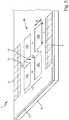
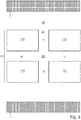
- Fig. 2 and 3 show an embodiment of the second variant of the invention.
- the dielectric interferer 9b arranged in the circuit board layer 3 preferably comprises a Waveguide arrangement 13 which has at least one dielectric waveguide segment R, S, T, U running in the circuit board layer 3.
- the waveguide arrangement 13 is preferably formed in that a metallization 15, 17, which has a structure formed by recesses in the respective metallization 15, 17, is applied to the top and a bottom of the circuit board layer 3.
- the structures comprise slot-line-shaped recesses which, in cooperation with the areas of the printed circuit board layer 3 enclosed between them, form the waveguide arrangement 13.
- the metallizations 15, 17 on the top and bottom in the area of the dielectric waveguide segments R, S, T, U have slot-line-shaped recesses of the same shape, lying one above the other, due to the arrangement, geometry and course of the dielectric ones delimited by the metallizations 15, 17 Areas of the circuit board layer 3 forming waveguide segments R, S, T, U are specified.
- the corresponding structuring of the metallization 15 applied to the top is shown in FIG Fig. 2 shown top view.
- the structuring of the metallization 17 applied to the underside of the circuit board layer 3 is shown in FIG Fig. 3 shown.
- a metallization-free area 19 is preferably provided between the high-frequency assembly 5 and the waveguide arrangement 13, in which no metallization is applied to the underside of the circuit board layer 3 and preferably also to the top of the circuit board layer 3. This ensures that this region 19 of the circuit board layer 3 acts as a planar dielectric waveguide, via which electromagnetic waves propagating in the circuit board layer 3 are guided in the direction of the dielectric interferer 9b.
- a single dielectric waveguide segment R, U preferably running transversely to the direction of propagation of the interference waves, disrupts the propagation of electromagnetic waves within the printed circuit board layer 3, and thus reduces mutual interference between adjacent assemblies.
- the direction of propagation denotes a direction dependent on the interference wave emission of the components provided on the circuit board 1 or in the circuit board 1, in which, without measures for interference suppression, those interference waves would propagate that would have the greatest or at least significant impairment of another Component would effect.
- the sensitivity of the other components to electromagnetic interference is also preferably taken into account. Assemblies regularly emit interference waves in all spatial directions or at least at a large opening angle. Accordingly, the direction of propagation is to be understood as a main direction in which the emitted interference radiation would exert the greatest negative influence without measures to suppress it.
- the waveguide arrangement 13 not only comprises a single waveguide segment, but a system, described in detail below, of several interconnected dielectric waveguide segments R, S, T, U.
- the waveguide arrangement 13 preferably includes an input 21 facing the high-frequency assembly (5), via which interference waves propagating in the circuit board layer 3 penetrate the waveguide system.
- the waveguide system preferably comprises four waveguide segments R, S, T, U connected to one another via a branch 23, two of which are connected to one another in a straight line via the branch 23 and run transversely to the direction of propagation of the interfering waves, and two are connected to one another in a straight line via the branch 23 and run parallel to the direction of propagation of the interference waves. All four waveguide segments R, S, T, U thus meet in the branch 23.
- the input 21 can be formed by the end of the waveguide segment T facing the high-frequency assembly 5.
- This embodiment is in the Figures 2 and 3 shown.
- an input shape is selected which brings about a low-reflection transition of the waves, which are dielectrically guided across the metallization-free region 19, into the waveguide segment T.
- This is achieved, for example, in that the slot-line-shaped recess, which predetermines the waveguide T, of the metallization 17 applied on the underside of the circuit board layer 3 is at the end in the direction of the high-frequency assembly 5 is widened. This can be a sudden expansion.
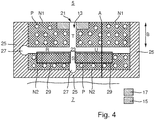
- Fig. 4 shows the metallizations 15, 17 of a corresponding modification of the circuit board 1 from FIG Fig. 2 and 3 , the two metallizations 15, 17 being shown one above the other and distinguishable by differently aligned hatching.
- a funnel-shaped or trumpet-shaped widening that becomes wider in the direction of the high-frequency assembly 5 can be provided.
- the dimensioning is preferably established as a function of a predetermined main frequency of the electromagnetic interference waves emanating from the high-frequency assembly 5.
- the waveguide segments R and U running transversely to the direction of propagation have a length that is equal to half the wavelength of the interference waves emitted at the main frequency in the respective waveguide segment R, U, and the waveguide segments S and T running parallel to the direction of propagation each have a length , which is equal to a quarter of the wavelength of the interference waves emitted at the main frequency in the respective waveguide segment S, T.
- the waveguide segments S and T running parallel to the direction of propagation each have a length , which is equal to a quarter of the wavelength of the interference waves emitted at the main frequency in the respective waveguide segment S, T.
- the portion reflected back on the input side in the waveguide segment T in the direction of the branch 23 is less than the portion reflected at the ends of the waveguide segments R, S, U.
- this is preferably compensated for in that the waveguide segments R, U running transversely to the direction of propagation are designed in such a way that they have a slightly greater impedance than the waveguide segments S, T connected in a straight line to the input 21 causes a slightly larger proportion to be conducted into the waveguide segments S, T via the branch 23.
- the impedance difference to be provided is usually of the order of a few percent, e.g. in the range of 5%.
- the metallizations 15, 17 on the top and bottom of the circuit board layer 3 are made in the Figures 2 and 3 illustrated embodiment of four spaced apart rectangular metal surfaces 15a, 15b, 15c, 15d, 17a, 17b, 17c, 17d whose length L, running perpendicular to the direction of propagation, corresponds to the length of the waveguide segments R or U, and whose width B corresponds to the length of the waveguide segments S or .T corresponds to.
- the individual metal surfaces 15a, 15b, 15c, 15 and 17a, 17b, 17c, 17d of the metallizations 15, 17 are spatially separated from one another, they effect a galvanic separation of the associated circuit board layer areas, which are used, for example, for explosion protection, to prevent ground loops, or can be used to implement different reference potentials for the high-frequency assembly 5 and the further assembly 7.
- the individual metal surfaces 17a, 17b, 17c, 17d of one of the metallizations 17 of the circuit board layer 3 are connected to one another in a conductive manner by bridges 25.
- the bridges 25 are applied flat outside the waveguide arrangement 13 on the corresponding side of the circuit board layer 3.
- This modification of the in Fig. 2 and 3 circuit board 1 shown is in the in Fig. 4
- the embodiment shown is provided in the case of the metallization 17 applied to the underside of the circuit board layer 3.
- the bridges 25 offer the advantage that the individual metal surfaces 17a, 17b, 17c, 17d are thereby at the same potential and thus form a more homogeneous delimitation for the elements of the dielectric waveguide arrangement 13.
- bridges can be provided for each of the metallizations 15, 17.
- a waveguide arrangement 13 with a broader band with regard to the desired destructive interference is achieved, however, in that only one of the two metallizations 15, 17 applied to the circuit board layer 3 is provided with bridges 25 becomes.
- that metallization 17 is preferably provided with bridges 25 which, on its side facing away from the circuit board layer 3, adjoins the layer having the greater dielectric constant. In the illustrated embodiment, this is the metallization 17 resting on a further circuit board layer 31 on the underside of the circuit board layer 3, since the circuit board layer 3 here forms the top layer of the circuit board 1, above which there is the ambient atmosphere, which has a lower dielectric constant than the further circuit board layer 31.
- dielectric waveguide arrangements are provided in several layers, preferably at least one and at most every second metallization is provided with bridges.
- the occurrence of destructive interference described above is limited to a narrow frequency band surrounding the main frequency due to the frequency-dependent dimensioning of the waveguide arrangement 13 required for this.
- This frequency band is preferably broadened in that one of the two waveguide segments R, U running transversely to the direction of propagation and the waveguide segment S running parallel to the direction of propagation on the side of the branch 23 facing away from the high-frequency assembly 5 are designed in such a way that they have a slightly shorter length on their upper side than on their underside.
- the metal surfaces 15a, 15c delimiting the waveguide segment R have a slightly smaller length than the corresponding length of the metal surfaces 17a, 17c located underneath of the metallization 17 applied to the underside.
- the metal surfaces 15c, 15d delimiting the waveguide segment S also have a slightly smaller length Width than the metal surfaces 17c, 17d located below of the metallization 17 applied to the underside.
- the ends of these two waveguide segments R, S preferably have a circular termination 27 on their undersides to further broaden the frequency band.
- a circular termination 27 is brought about by a corresponding circular recess, here arranged within the corresponding two bridges 25, in the metallization 17 of the underside of the circuit board layer 3.
- the waveguide arrangement 13 In addition to the disruption and partial destruction of interference waves propagating within the circuit board layer 3, the waveguide arrangement 13 also causes interference with interference waves propagating on the circuit board layer 3.
- part of the interference waves that may emanate from the further assembly 7 and propagate on the top of the circuit board layer 3 in the direction of the high-frequency assembly 5 is reflected on the edge N2 of the metallization 15 of the top facing the further assembly 7.
- the respective edge N1, N2 brings about a reduction in the mutual impairment of the two assemblies.
- the portion of the interference waves picked up in this way by the waveguide arrangement 13 depends largely on the width B of the metal surfaces 15a, 15b, 15c, 15d adjoining the respective edge N1, N2 and the wavelength of the interference waves above the circuit board layer 3.
- These widths B also specify the lengths of the waveguide segments T, S running parallel to the direction of propagation.
- the widths B are preferably specified in such a way that the total interference suppression caused by both the interference wave components entering the waveguide arrangement 13 from above and the interference wave components destructively interfering in the waveguide arrangement 13 is maximum.
- waveguide arrangements can of course also be used which have waveguide segments connected to one another or arranged in a different way.
- Fig. 4 Vias P shown are provided, via which the metal surfaces 15a, 15b, 15c, 15d of the metallization 15 on the top of the circuit board layer 3 are conductively connected to the metal surfaces 17a, 17b, 17c, 17d of the metallization 17 on the underside of the circuit board layer 3 located below.
- the section of the printed circuit board layer 3 located between two plated-through holes acts like a metallic waveguide, the cut-off frequency of which can be adjusted by its dimensioning and the dielectric properties of the printed circuit board layer 3.
- interference signals with frequencies below the cut-off frequency cannot propagate in the metallic waveguide.
- the plated-through holes P can be distributed everywhere over the metal surfaces 15a, 15b, 15c, 15d of the metallization 15 of the top side of the circuit board layer 3, under which one of the Metal surfaces 17a, 17b, 17c, 17d of the metallization 17 of the underside of the circuit board layer 3 is located.
- the areas 29 adjacent to the waveguide segments R and U running transversely to the direction of propagation are preferably cut out on their side facing the further assembly 7. That is to say, in these two areas 29 of the metal surfaces 15c, 15d, no plated-through holes P are preferably provided.
- the via-free areas 29 are shown in FIG Fig. 4 highlighted by a frame.
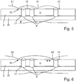
- the interfering wave S1, S2 strikes the printed circuit board layer 3 at an impact point X1, X2 that is dependent on its wavelength. If this point of impact is X1, as in Fig. 5 shown, in the area of the waveguide segment U, the interfering wave S1 at least partially enters the waveguide arrangement 13, and thus no longer causes any interference in the further assembly 7.
- a field distribution is formed through which part of the interfering wave S2 is led back into the waveguide segment U. This is in Fig. 6 indicated by an arrow.
- the part that is led back to the waveguide segment U is larger, the closer the point of impact X2 is to the dielectric waveguide U.
- Interfering waves impinging behind the first via P in the direction of propagation cannot, however, be fed back into the dielectric waveguide arrangement 13.
- the waveguide arrangement 13 is optimized, in particular via the positioning of the input 21 and the via-free areas 29, to reduce the transmission of interference waves from the high-frequency assembly 5 in the direction of the further assembly 7, it also acts in the opposite direction. That is, a transmission of high-frequency interference waves from the further assembly 7 in the direction of the high-frequency assembly 5 is also disturbed by the waveguide arrangement 13 in the ways described above.
- waveguide arrangements 13 can be provided in the circuit board layer 3.
- the waveguide assemblies 13 can e.g. be arranged distributed over the circuit board 1 in an orthogonal or hexagonal grid in such a way that they surround one or more assemblies arranged within a grid field, in particular high-frequency assemblies, on almost all sides.
- the waveguide arrangements 13 can be arranged both in the topmost circuit board layer 3 and in one or more inner circuit board layers 3.
- the two variants of the invention i.e. one or more dielectric interferers 9a applied above the circuit board layer 3 and one or more dielectric interferers 9b arranged in the circuit board layer 3, can also be used in combination with one another spatially adjacent to one another in a circuit board 1.
Landscapes
- Engineering & Computer Science (AREA)
- Microelectronics & Electronic Packaging (AREA)
- Physics & Mathematics (AREA)
- Electromagnetism (AREA)
- Shielding Devices Or Components To Electric Or Magnetic Fields (AREA)
- Waveguide Connection Structure (AREA)
- Structure Of Printed Boards (AREA)
Claims (18)
- Carte de circuit imprimé (1) avec- une couche de circuit imprimé (3), sur laquelle sont prévus un composant haute fréquence (5) émettant, en fonctionnement, des ondes électromagnétiques perturbatrices de haute fréquence, et au moins un composant supplémentaire (7), notamment un autre composant haute fréquence,
caractérisé- en ce qu'est prévu, entre le composant haute fréquence (5) et le composant supplémentaire (7), au moins un perturbateur diélectrique (9a, 9b), qui perturbe une propagation des ondes électromagnétiques perturbatrices de haute fréquence entre le composant haute fréquence (5) et le composant supplémentaire (7), et- en ce qu'est prévu, sous la couche de circuit imprimé (3), un couche de circuit imprimé supplémentaire (31) constituée d'un matériau amortissant les ondes électromagnétiques de haute fréquence, notamment des nattes de fibres de verre imprégnées de résine époxy. - Carte de circuit imprimé selon la revendication 1, caractérisée en ce qu'un perturbateur diélectrique (9a) est un corps placé sur une face supérieure de la couche de circuit imprimé (3), lequel corps est constitué d'un diélectrique, notamment un noyau diélectrique d'un composant placé sur une piste métallique (11) sur la face supérieure de la couche de circuit imprimé (3), notamment une résistance ou un condensateur.
- Carte de circuit imprimé selon la revendication 1, caractérisée en ce qu'au moins un perturbateur diélectrique (9a) est un dispositif de guide d'ondes diélectrique (13), disposé dans la couche de circuit imprimé (3).
- Carte de circuit imprimé selon la revendication 3, caractérisée en ce que le dispositif de guide d'ondes diélectrique (13) présente au moins un segment de guide d'ondes (R, U) s'étendant perpendiculairement à une direction de propagation des ondes perturbatrices.
- Carte de circuit imprimé selon la revendication 3, caractérisée en ce que le dispositif de guide d'ondes (13) comprend des segments de guide d'ondes (R, S, T, U) reliés entre eux via une dérivation (23),- segments parmi lesquels deux sont reliés entre eux en ligne droite via la dérivation (23) et s'étendent perpendiculairement à une direction de propagation des ondes perturbatrices, et- segments parmi lesquels deux sont reliés entre eux en ligne droite via la dérivation (23) et s'étendent parallèlement à une direction de propagation des ondes perturbatrices.
- Carte de circuit imprimé selon la revendication 5, caractérisée en ce que- en fonctionnement, les ondes perturbatrices - entrant dans le dispositif de guide d'ondes (13) au niveau de la dérivation (23) via le segment de guide d'ondes (T) faisant face au composant haute fréquence (5) et s'étendant parallèlement à la direction de propagation des ondes perturbatrices - sont divisées au niveau de la dérivation (23) en ondes partielles se propageant dans les segments de guide d'ondes (R, S, U) restants,- ces ondes partielles sont réfléchies aux extrémités des segments de guide d'ondes (R, S, T, U), et- les segments de guide d'ondes (R, S, T, U) présentent des longueurs prédéfinies en fonction d'une fréquence principale prédéfinie des ondes perturbatrices, longueurs auxquelles des ondes partielles d'ondes perturbatrices entrantes de la fréquence principale se superposent de manière destructive dans le dispositif de guide d'ondes (13) avec des ondes partielles réfléchies aux extrémités des segments de guide d'ondes (R, S, T, U).
- Carte de circuit imprimé selon la revendication 6, caractérisée en ce que- les segments de guide d'ondes (R, U) s'étendant perpendiculairement à la direction de propagation des ondes perturbatrices présentent une longueur correspondant à la moitié d'une longueur d'onde des ondes perturbatrices ayant la fréquence principale dans ces segments de guide d'ondes (R, U), et- les segments de guide d'ondes (S, T) s'étendant parallèlement à la direction de propagation des ondes perturbatrices présentent une longueur correspondant à un quart de la longueur d'onde des ondes perturbatrices ayant la fréquence principale dans ces segments de guide d'ondes (S, T).
- Carte de circuit imprimé selon la revendication 6, caractérisée en ce que le dispositif de guide d'ondes (13) présente une entrée (21) tournée vers le composant haute fréquence (5), qui débouche dans le segment de guide d'ondes (T) tourné vers le composant haute fréquence (5) et s'étendant parallèlement à la direction de propagation des ondes perturbatrices.
- Carte de circuit imprimé selon la revendication 6, caractérisée en ce que les segments de guide d'ondes (S, T) connectés en ligne droite à l'entrée (23) présentent une impédance plus faible que les autres segments de guide d'ondes (R, U).
- Carte de circuit imprimé selon la revendication 3, caractérisée en ce que le dispositif de guides d'ondes (13) est formé par une zone de la couche de circuit imprimé (3), dans laquelle- une métallisation (15, 17) est appliquée respectivement sur la face supérieure et sur la face inférieure de la couche de circuit imprimé (3),- les métallisations (15, 17) présentent chacune une structure formée par des évidements dans la métallisation, et- les structures, associées aux zones de la couche de circuit imprimé (3) enfermées entre elles, forment le dispositif de guides d'ondes (13).
- Carte de circuit imprimé selon la revendication 10, caractérisée en ce que les métallisations (15, 17) sont constituées de surfaces métalliques (15a, 15b, 15c, 15d, 17a, 17b, 17c, 17d) spatialement séparées les unes des autres.
- Carte de circuit imprimé selon la revendication 10, caractérisée en ce que les surfaces métalliques (17a, 17b, 17c, 17d) de l'une des métallisations (17), notamment les surfaces métalliques (17a, 17b, 17c, 17d) de la métallisation (17) prévue sur la face inférieure de la couche de circuit imprimé (3), sont reliées entre elles de manière conductrice par des ponts (25) appliqués sur la couche de circuit imprimé (3) à l'extérieur du dispositif de guides d'ondes (13).
- Carte de circuit imprimé selon la revendication 8 et 10, caractérisée en ce que l'entrée (21) est formée par des évidements dans la métallisation (17) sur la face inférieure de la couche de circuit imprimé (3).
- Carte de circuit imprimé selon la revendication 5, caractérisée en ce que l'un des segments de guide d'ondes (R) s'étendant perpendiculairement à la direction de propagation des ondes perturbatrices et le segment de guide d'ondes (S) s'étendant parallèlement à la direction de propagation sur le côté de la dérivation (23) situé à l'opposé du composant haute fréquence (5) sont conçus de telle manière qu'ils présentent une longueur légèrement plus courte sur leur face supérieure que sur leur face inférieure.
- Carte de circuit imprimé selon la revendication 14, caractérisée en ce que le segment de guide d'ondes (R) s'étendant perpendiculairement à la direction de propagation des ondes perturbatrices et le segment de guide d'ondes (S) s'étendant parallèlement à la direction de propagation sur le côté de la dérivation (23) situé à l'opposé du composant haute fréquence (5) présentent chacun une terminaison circulaire (27) sur leur face inférieure.
- Carte de circuit imprimé selon la revendication 10, caractérisée en ce que des trous traversants (P) sont prévus, par l'intermédiaire lesquels la métallisation (15) sur la face supérieure de la couche de circuit imprimé (3) est reliée de manière conductrice à la métallisation (17) située en dessous sur la face inférieure de la couche de circuit imprimé (3).
- Carte de circuit imprimé selon la revendication 16, caractérisée en ce que sur les côtés des segments de guide d'ondes (R, U) s'étendant perpendiculairement à la direction de propagation des ondes perturbatrices sont prévues des zones (29) exemptes de trous traversants, qui font face au composant supplémentaire (7), directement adjacent à ces segments de guide d'ondes (R, U).
- Carte de circuit imprimé selon la revendication 10, caractérisée en ce qu'est prévue, entre le composant haute fréquence (5) et le dispositif de guide d'ondes (13), une zone exempte de métallisation (19) sur le dessous de la couche de circuit imprimé (3).
Applications Claiming Priority (2)
| Application Number | Priority Date | Filing Date | Title |
|---|---|---|---|
| DE102012106174.2A DE102012106174A1 (de) | 2012-07-10 | 2012-07-10 | Mit einer Störwellen aussendenden Hochfrequenzbaugruppe ausgestattete Leiterplatte |
| PCT/EP2013/061808 WO2014009069A2 (fr) | 2012-07-10 | 2013-06-07 | Circuit imprimé équipé d'un sous-ensemble à haute fréquence émettant des ondes parasites |
Publications (2)
| Publication Number | Publication Date |
|---|---|
| EP2873308A2 EP2873308A2 (fr) | 2015-05-20 |
| EP2873308B1 true EP2873308B1 (fr) | 2020-12-23 |
Family
ID=48652014
Family Applications (1)
| Application Number | Title | Priority Date | Filing Date |
|---|---|---|---|
| EP13729650.5A Not-in-force EP2873308B1 (fr) | 2012-07-10 | 2013-06-07 | Circuit imprimé équipé d'un sous-ensemble à haute fréquence émettant des ondes parasites |
Country Status (5)
| Country | Link |
|---|---|
| US (1) | US9801268B2 (fr) |
| EP (1) | EP2873308B1 (fr) |
| CN (1) | CN104488365B (fr) |
| DE (1) | DE102012106174A1 (fr) |
| WO (1) | WO2014009069A2 (fr) |
Families Citing this family (11)
| Publication number | Priority date | Publication date | Assignee | Title |
|---|---|---|---|---|
| BRPI0706368A2 (pt) | 2006-01-06 | 2011-03-22 | Univ Georgia | composição, vetor, método para fornecer resistência ao cisto nematódeo a uma planta, proteìna de fusão, método para inibir atividade biológica, ácido nucléico isolado |
| WO2011034945A1 (fr) | 2009-09-15 | 2011-03-24 | Metabolix, Inc. | Génération d'oléagineux produisant des taux élevés de polyhydroxybutrate |
| BR112013005973A2 (pt) | 2010-09-15 | 2019-09-24 | Metabolix Inc | aumento do fluxo de carbono para a produção de poli-hidroxibutirato em culturas de biomassa |
| US11174467B2 (en) | 2015-04-08 | 2021-11-16 | Yield10 Bioscience, Inc. | Plants with enhanced yield and methods of construction |
| US20190338302A1 (en) | 2016-02-04 | 2019-11-07 | Yield10 Bioscience, Inc. | Transgenic land plants comprising a putative transporter protein of an edible eukaryotic algae |
| EP3585149A4 (fr) | 2017-02-22 | 2020-10-28 | Yield10 Bioscience, Inc. | Plantes terrestres transgéniques comprenant des teneurs améliorées en protéine transporteuse mitochondriale |
| HUE047827T2 (hu) * | 2017-10-06 | 2020-05-28 | Grieshaber Vega Kg | Radaros szintmérõ szinkronizáló jellel áramköri lap különbözõ rétegein |
| EP3846615A4 (fr) | 2018-09-04 | 2022-05-25 | Yield10 Bioscience, Inc. | Plantes terrestres génétiquement modifiées exprimant une protéine d'amélioration du rendement en graines et/ou un arn d'amélioration du rendement en graines |
| US12116583B2 (en) | 2019-05-14 | 2024-10-15 | Yield10 Bioscience, Inc. | Modified plants comprising a polynucleotide comprising a non-cognate promoter operably linked to a coding sequence that encodes a transcription factor |
| WO2024158934A1 (fr) | 2023-01-24 | 2024-08-02 | Yale University | Compositions et procédés de régulation du nombre de copies d'adn-t dans des plantes modifiées |
| WO2024166076A1 (fr) | 2023-02-10 | 2024-08-15 | King Abdullah University Of Science And Technology | Production recombinée de peptides antimicrobiens in planta |
Family Cites Families (16)
| Publication number | Priority date | Publication date | Assignee | Title |
|---|---|---|---|---|
| JPS58120301A (ja) | 1982-01-12 | 1983-07-18 | Sony Corp | 帯域通過フイルタ |
| US4602229A (en) * | 1983-12-30 | 1986-07-22 | Motorola, Inc. | Resonant bandpass T filter and power splitter |
| US5185690A (en) * | 1991-10-16 | 1993-02-09 | Miller Mark L | High dielectric constant sheet material |
| US5714919A (en) | 1993-10-12 | 1998-02-03 | Matsushita Electric Industrial Co., Ltd. | Dielectric notch resonator and filter having preadjusted degree of coupling |
| SE512166C2 (sv) * | 1997-11-21 | 2000-02-07 | Ericsson Telefon Ab L M | Mikrostripanordning |
| US6194981B1 (en) | 1999-04-01 | 2001-02-27 | Endwave Corporation | Slot line band reject filter |
| US20030080826A1 (en) | 2001-10-30 | 2003-05-01 | Walker Chen | Method of shortening a microwave circuit and the printed circuit board made by using said method |
| CN1509132A (zh) | 2002-12-18 | 2004-06-30 | 矽统科技股份有限公司 | 功率分配系统的共振频率的调离方法 |
| JP4418250B2 (ja) * | 2004-02-05 | 2010-02-17 | 株式会社ルネサステクノロジ | 高周波回路モジュール |
| WO2006022104A1 (fr) | 2004-08-24 | 2006-03-02 | Murata Manufacturing Co., Ltd. | Structure de connexion de ligne de transmission et transmetteur/récepteur |
| JP2007166115A (ja) * | 2005-12-12 | 2007-06-28 | Matsushita Electric Ind Co Ltd | アンテナ装置 |
| JP4936391B2 (ja) * | 2007-11-07 | 2012-05-23 | 北川工業株式会社 | セラミックシート |
| JP5326649B2 (ja) | 2009-02-24 | 2013-10-30 | 日本電気株式会社 | アンテナ、アレイアンテナ、プリント基板、及びそれを用いた電子装置 |
| CN102792519A (zh) | 2010-03-08 | 2012-11-21 | 日本电气株式会社 | 结构、线路板和制造线路板的方法 |
| DE102010061714B4 (de) | 2010-11-22 | 2023-09-21 | Endress+Hauser SE+Co. KG | Elektronikeinheit mit Abschirmung |
| US8680403B2 (en) * | 2011-09-08 | 2014-03-25 | Texas Instruments Incorporated | Apparatus for broadband matching |
-
2012
- 2012-07-10 DE DE102012106174.2A patent/DE102012106174A1/de not_active Withdrawn
-
2013
- 2013-06-07 EP EP13729650.5A patent/EP2873308B1/fr not_active Not-in-force
- 2013-06-07 WO PCT/EP2013/061808 patent/WO2014009069A2/fr not_active Ceased
- 2013-06-07 CN CN201380036730.0A patent/CN104488365B/zh not_active Expired - Fee Related
- 2013-06-07 US US14/413,431 patent/US9801268B2/en not_active Expired - Fee Related
Non-Patent Citations (1)
| Title |
|---|
| None * |
Also Published As
| Publication number | Publication date |
|---|---|
| US9801268B2 (en) | 2017-10-24 |
| DE102012106174A1 (de) | 2014-01-16 |
| CN104488365B (zh) | 2018-07-17 |
| WO2014009069A3 (fr) | 2014-03-20 |
| WO2014009069A2 (fr) | 2014-01-16 |
| EP2873308A2 (fr) | 2015-05-20 |
| CN104488365A (zh) | 2015-04-01 |
| US20150156861A1 (en) | 2015-06-04 |
Similar Documents
| Publication | Publication Date | Title |
|---|---|---|
| EP2873308B1 (fr) | Circuit imprimé équipé d'un sous-ensemble à haute fréquence émettant des ondes parasites | |
| EP0766099B1 (fr) | Module radar à Doppler | |
| DE69304205T2 (de) | Verminderungsmittel von elektromagnetischer strahlung mit verwendung von geerdeten leiterbahnen,die die innere ebenen einer leiterplatte einfassen | |
| EP3100070B1 (fr) | Système de radar permettant de détecter l'environnement d'un véhicule | |
| EP1196017B1 (fr) | Dispositif de filtrage | |
| DE112017002142B4 (de) | Millimeterwellenband-kommunikationsgerät | |
| EP2158636A1 (fr) | Système coplanaire de guides d'ondes contrôle par impédance pour la distribution tridimensionnelle de signaux de grande largeur de bande | |
| DE112018004977B4 (de) | Hochfrequenzübertragungsleitung | |
| WO2015180820A1 (fr) | Boîtier blindé contre les hautes fréquences, en particulier boîtier de filtre blindé contre les hautes fréquences | |
| EP3134748B1 (fr) | Système de radar pour détecter les environs d'un véhicule et circuit imprimé pour un tel système de radar | |
| EP2609796B1 (fr) | Carte de circuits imprimés multiniveau pour applications haute fréquence | |
| DE102017216906A1 (de) | Wellenleitersystem, Hochfrequenzleitung und Radarsensor | |
| DE112021001460T5 (de) | Doppelseitige Platte, Radarvorrichtung, Übertragungselement, und Verfahren zum Herstellen eines Übertragungselements | |
| DE10040142A1 (de) | Schaltungsbauteil und Leiterplattenmodul | |
| DE19918583C2 (de) | Dielektrische Resonatorvorrichtung | |
| DE102015011182B4 (de) | HF-Filter in cavity Bauweise mit einer Umgehungsleitung für niederfrequente Signale und Spannungen | |
| DE102012110787A1 (de) | Koppelstruktur zur galvanisch trennenden signalübertragung, kommunikationsstruktur und wechselrichter | |
| DE102008051531B4 (de) | Elektrisches System mit einer Vorrichtung zur Unterdrückung der Ausbreitung einer elektromagnetischen Störung | |
| DE202017100322U1 (de) | Filterstruktur mit Verbesserungen | |
| EP1744363B1 (fr) | Circuit intégré monolithique avec réduction de bruit intégré | |
| DE102019214126A1 (de) | Antennenvorrichtung und Fahrzeug aufweisend eine Antennenvorrichtung | |
| EP2137787B1 (fr) | Séparateur de tension continue | |
| DE102005037950B3 (de) | Ein Verfahren zum vereinfachten Aufbau von Mikrowellenschaltungen in LTCC-Technik mit reduzierter Anzahl von Durchgangslöchern | |
| EP4293815A1 (fr) | Dispositif radar | |
| DE102023113912A1 (de) | Radaranordnung |
Legal Events
| Date | Code | Title | Description |
|---|---|---|---|
| PUAI | Public reference made under article 153(3) epc to a published international application that has entered the european phase |
Free format text: ORIGINAL CODE: 0009012 |
|
| 17P | Request for examination filed |
Effective date: 20141210 |
|
| AK | Designated contracting states |
Kind code of ref document: A2 Designated state(s): AL AT BE BG CH CY CZ DE DK EE ES FI FR GB GR HR HU IE IS IT LI LT LU LV MC MK MT NL NO PL PT RO RS SE SI SK SM TR |
|
| AX | Request for extension of the european patent |
Extension state: BA ME |
|
| DAX | Request for extension of the european patent (deleted) | ||
| RAP1 | Party data changed (applicant data changed or rights of an application transferred) |
Owner name: ENDRESS+HAUSER SE+CO. KG |
|
| STAA | Information on the status of an ep patent application or granted ep patent |
Free format text: STATUS: EXAMINATION IS IN PROGRESS |
|
| 17Q | First examination report despatched |
Effective date: 20180508 |
|
| GRAP | Despatch of communication of intention to grant a patent |
Free format text: ORIGINAL CODE: EPIDOSNIGR1 |
|
| STAA | Information on the status of an ep patent application or granted ep patent |
Free format text: STATUS: GRANT OF PATENT IS INTENDED |
|
| RIC1 | Information provided on ipc code assigned before grant |
Ipc: H05K 1/02 20060101AFI20200716BHEP Ipc: H01P 3/02 20060101ALN20200716BHEP Ipc: H01P 1/201 20060101ALN20200716BHEP |
|
| RIC1 | Information provided on ipc code assigned before grant |
Ipc: H01P 3/02 20060101ALN20200722BHEP Ipc: H01P 1/201 20060101ALN20200722BHEP Ipc: H05K 1/02 20060101AFI20200722BHEP |
|
| INTG | Intention to grant announced |
Effective date: 20200813 |
|
| GRAS | Grant fee paid |
Free format text: ORIGINAL CODE: EPIDOSNIGR3 |
|
| GRAA | (expected) grant |
Free format text: ORIGINAL CODE: 0009210 |
|
| STAA | Information on the status of an ep patent application or granted ep patent |
Free format text: STATUS: THE PATENT HAS BEEN GRANTED |
|
| AK | Designated contracting states |
Kind code of ref document: B1 Designated state(s): AL AT BE BG CH CY CZ DE DK EE ES FI FR GB GR HR HU IE IS IT LI LT LU LV MC MK MT NL NO PL PT RO RS SE SI SK SM TR |
|
| REG | Reference to a national code |
Ref country code: GB Ref legal event code: FG4D Free format text: NOT ENGLISH |
|
| REG | Reference to a national code |
Ref country code: DE Ref legal event code: R096 Ref document number: 502013015393 Country of ref document: DE |
|
| REG | Reference to a national code |
Ref country code: AT Ref legal event code: REF Ref document number: 1348969 Country of ref document: AT Kind code of ref document: T Effective date: 20210115 |
|
| REG | Reference to a national code |
Ref country code: IE Ref legal event code: FG4D Free format text: LANGUAGE OF EP DOCUMENT: GERMAN |
|
| PG25 | Lapsed in a contracting state [announced via postgrant information from national office to epo] |
Ref country code: NO Free format text: LAPSE BECAUSE OF FAILURE TO SUBMIT A TRANSLATION OF THE DESCRIPTION OR TO PAY THE FEE WITHIN THE PRESCRIBED TIME-LIMIT Effective date: 20210323 Ref country code: RS Free format text: LAPSE BECAUSE OF FAILURE TO SUBMIT A TRANSLATION OF THE DESCRIPTION OR TO PAY THE FEE WITHIN THE PRESCRIBED TIME-LIMIT Effective date: 20201223 Ref country code: FI Free format text: LAPSE BECAUSE OF FAILURE TO SUBMIT A TRANSLATION OF THE DESCRIPTION OR TO PAY THE FEE WITHIN THE PRESCRIBED TIME-LIMIT Effective date: 20201223 Ref country code: GR Free format text: LAPSE BECAUSE OF FAILURE TO SUBMIT A TRANSLATION OF THE DESCRIPTION OR TO PAY THE FEE WITHIN THE PRESCRIBED TIME-LIMIT Effective date: 20210324 |
|
| REG | Reference to a national code |
Ref country code: NL Ref legal event code: MP Effective date: 20201223 |
|
| PG25 | Lapsed in a contracting state [announced via postgrant information from national office to epo] |
Ref country code: SE Free format text: LAPSE BECAUSE OF FAILURE TO SUBMIT A TRANSLATION OF THE DESCRIPTION OR TO PAY THE FEE WITHIN THE PRESCRIBED TIME-LIMIT Effective date: 20201223 Ref country code: LV Free format text: LAPSE BECAUSE OF FAILURE TO SUBMIT A TRANSLATION OF THE DESCRIPTION OR TO PAY THE FEE WITHIN THE PRESCRIBED TIME-LIMIT Effective date: 20201223 Ref country code: BG Free format text: LAPSE BECAUSE OF FAILURE TO SUBMIT A TRANSLATION OF THE DESCRIPTION OR TO PAY THE FEE WITHIN THE PRESCRIBED TIME-LIMIT Effective date: 20210323 |
|
| PG25 | Lapsed in a contracting state [announced via postgrant information from national office to epo] |
Ref country code: HR Free format text: LAPSE BECAUSE OF FAILURE TO SUBMIT A TRANSLATION OF THE DESCRIPTION OR TO PAY THE FEE WITHIN THE PRESCRIBED TIME-LIMIT Effective date: 20201223 Ref country code: NL Free format text: LAPSE BECAUSE OF FAILURE TO SUBMIT A TRANSLATION OF THE DESCRIPTION OR TO PAY THE FEE WITHIN THE PRESCRIBED TIME-LIMIT Effective date: 20201223 |
|
| REG | Reference to a national code |
Ref country code: LT Ref legal event code: MG9D |
|
| PG25 | Lapsed in a contracting state [announced via postgrant information from national office to epo] |
Ref country code: RO Free format text: LAPSE BECAUSE OF FAILURE TO SUBMIT A TRANSLATION OF THE DESCRIPTION OR TO PAY THE FEE WITHIN THE PRESCRIBED TIME-LIMIT Effective date: 20201223 Ref country code: PT Free format text: LAPSE BECAUSE OF FAILURE TO SUBMIT A TRANSLATION OF THE DESCRIPTION OR TO PAY THE FEE WITHIN THE PRESCRIBED TIME-LIMIT Effective date: 20210423 Ref country code: SK Free format text: LAPSE BECAUSE OF FAILURE TO SUBMIT A TRANSLATION OF THE DESCRIPTION OR TO PAY THE FEE WITHIN THE PRESCRIBED TIME-LIMIT Effective date: 20201223 Ref country code: LT Free format text: LAPSE BECAUSE OF FAILURE TO SUBMIT A TRANSLATION OF THE DESCRIPTION OR TO PAY THE FEE WITHIN THE PRESCRIBED TIME-LIMIT Effective date: 20201223 Ref country code: EE Free format text: LAPSE BECAUSE OF FAILURE TO SUBMIT A TRANSLATION OF THE DESCRIPTION OR TO PAY THE FEE WITHIN THE PRESCRIBED TIME-LIMIT Effective date: 20201223 Ref country code: CZ Free format text: LAPSE BECAUSE OF FAILURE TO SUBMIT A TRANSLATION OF THE DESCRIPTION OR TO PAY THE FEE WITHIN THE PRESCRIBED TIME-LIMIT Effective date: 20201223 Ref country code: SM Free format text: LAPSE BECAUSE OF FAILURE TO SUBMIT A TRANSLATION OF THE DESCRIPTION OR TO PAY THE FEE WITHIN THE PRESCRIBED TIME-LIMIT Effective date: 20201223 |
|
| PG25 | Lapsed in a contracting state [announced via postgrant information from national office to epo] |
Ref country code: PL Free format text: LAPSE BECAUSE OF FAILURE TO SUBMIT A TRANSLATION OF THE DESCRIPTION OR TO PAY THE FEE WITHIN THE PRESCRIBED TIME-LIMIT Effective date: 20201223 |
|
| REG | Reference to a national code |
Ref country code: DE Ref legal event code: R097 Ref document number: 502013015393 Country of ref document: DE |
|
| PG25 | Lapsed in a contracting state [announced via postgrant information from national office to epo] |
Ref country code: IS Free format text: LAPSE BECAUSE OF FAILURE TO SUBMIT A TRANSLATION OF THE DESCRIPTION OR TO PAY THE FEE WITHIN THE PRESCRIBED TIME-LIMIT Effective date: 20210423 |
|
| PG25 | Lapsed in a contracting state [announced via postgrant information from national office to epo] |
Ref country code: AL Free format text: LAPSE BECAUSE OF FAILURE TO SUBMIT A TRANSLATION OF THE DESCRIPTION OR TO PAY THE FEE WITHIN THE PRESCRIBED TIME-LIMIT Effective date: 20201223 |
|
| PLBE | No opposition filed within time limit |
Free format text: ORIGINAL CODE: 0009261 |
|
| STAA | Information on the status of an ep patent application or granted ep patent |
Free format text: STATUS: NO OPPOSITION FILED WITHIN TIME LIMIT |
|
| PG25 | Lapsed in a contracting state [announced via postgrant information from national office to epo] |
Ref country code: DK Free format text: LAPSE BECAUSE OF FAILURE TO SUBMIT A TRANSLATION OF THE DESCRIPTION OR TO PAY THE FEE WITHIN THE PRESCRIBED TIME-LIMIT Effective date: 20201223 Ref country code: ES Free format text: LAPSE BECAUSE OF FAILURE TO SUBMIT A TRANSLATION OF THE DESCRIPTION OR TO PAY THE FEE WITHIN THE PRESCRIBED TIME-LIMIT Effective date: 20201223 |
|
| 26N | No opposition filed |
Effective date: 20210924 |
|
| PG25 | Lapsed in a contracting state [announced via postgrant information from national office to epo] |
Ref country code: MC Free format text: LAPSE BECAUSE OF FAILURE TO SUBMIT A TRANSLATION OF THE DESCRIPTION OR TO PAY THE FEE WITHIN THE PRESCRIBED TIME-LIMIT Effective date: 20201223 |
|
| REG | Reference to a national code |
Ref country code: CH Ref legal event code: PL |
|
| GBPC | Gb: european patent ceased through non-payment of renewal fee |
Effective date: 20210607 |
|
| PG25 | Lapsed in a contracting state [announced via postgrant information from national office to epo] |
Ref country code: SI Free format text: LAPSE BECAUSE OF FAILURE TO SUBMIT A TRANSLATION OF THE DESCRIPTION OR TO PAY THE FEE WITHIN THE PRESCRIBED TIME-LIMIT Effective date: 20201223 |
|
| REG | Reference to a national code |
Ref country code: BE Ref legal event code: MM Effective date: 20210630 |
|
| PG25 | Lapsed in a contracting state [announced via postgrant information from national office to epo] |
Ref country code: LU Free format text: LAPSE BECAUSE OF NON-PAYMENT OF DUE FEES Effective date: 20210607 |
|
| PG25 | Lapsed in a contracting state [announced via postgrant information from national office to epo] |
Ref country code: LI Free format text: LAPSE BECAUSE OF NON-PAYMENT OF DUE FEES Effective date: 20210630 Ref country code: IE Free format text: LAPSE BECAUSE OF NON-PAYMENT OF DUE FEES Effective date: 20210607 Ref country code: GB Free format text: LAPSE BECAUSE OF NON-PAYMENT OF DUE FEES Effective date: 20210607 Ref country code: CH Free format text: LAPSE BECAUSE OF NON-PAYMENT OF DUE FEES Effective date: 20210630 |
|
| PG25 | Lapsed in a contracting state [announced via postgrant information from national office to epo] |
Ref country code: IS Free format text: LAPSE BECAUSE OF FAILURE TO SUBMIT A TRANSLATION OF THE DESCRIPTION OR TO PAY THE FEE WITHIN THE PRESCRIBED TIME-LIMIT Effective date: 20210423 Ref country code: FR Free format text: LAPSE BECAUSE OF NON-PAYMENT OF DUE FEES Effective date: 20210630 |
|
| PG25 | Lapsed in a contracting state [announced via postgrant information from national office to epo] |
Ref country code: BE Free format text: LAPSE BECAUSE OF NON-PAYMENT OF DUE FEES Effective date: 20210630 |
|
| REG | Reference to a national code |
Ref country code: AT Ref legal event code: MM01 Ref document number: 1348969 Country of ref document: AT Kind code of ref document: T Effective date: 20210607 |
|
| PG25 | Lapsed in a contracting state [announced via postgrant information from national office to epo] |
Ref country code: AT Free format text: LAPSE BECAUSE OF NON-PAYMENT OF DUE FEES Effective date: 20210607 |
|
| PG25 | Lapsed in a contracting state [announced via postgrant information from national office to epo] |
Ref country code: HU Free format text: LAPSE BECAUSE OF FAILURE TO SUBMIT A TRANSLATION OF THE DESCRIPTION OR TO PAY THE FEE WITHIN THE PRESCRIBED TIME-LIMIT; INVALID AB INITIO Effective date: 20130607 |
|
| PG25 | Lapsed in a contracting state [announced via postgrant information from national office to epo] |
Ref country code: CY Free format text: LAPSE BECAUSE OF FAILURE TO SUBMIT A TRANSLATION OF THE DESCRIPTION OR TO PAY THE FEE WITHIN THE PRESCRIBED TIME-LIMIT Effective date: 20201223 |
|
| P01 | Opt-out of the competence of the unified patent court (upc) registered |
Effective date: 20230601 |
|
| PGFP | Annual fee paid to national office [announced via postgrant information from national office to epo] |
Ref country code: DE Payment date: 20230620 Year of fee payment: 11 |
|
| PGFP | Annual fee paid to national office [announced via postgrant information from national office to epo] |
Ref country code: IT Payment date: 20230623 Year of fee payment: 11 |
|
| PG25 | Lapsed in a contracting state [announced via postgrant information from national office to epo] |
Ref country code: MK Free format text: LAPSE BECAUSE OF FAILURE TO SUBMIT A TRANSLATION OF THE DESCRIPTION OR TO PAY THE FEE WITHIN THE PRESCRIBED TIME-LIMIT Effective date: 20201223 |
|
| PG25 | Lapsed in a contracting state [announced via postgrant information from national office to epo] |
Ref country code: MT Free format text: LAPSE BECAUSE OF FAILURE TO SUBMIT A TRANSLATION OF THE DESCRIPTION OR TO PAY THE FEE WITHIN THE PRESCRIBED TIME-LIMIT Effective date: 20201223 |
|
| REG | Reference to a national code |
Ref country code: DE Ref legal event code: R119 Ref document number: 502013015393 Country of ref document: DE |
|
| PG25 | Lapsed in a contracting state [announced via postgrant information from national office to epo] |
Ref country code: DE Free format text: LAPSE BECAUSE OF NON-PAYMENT OF DUE FEES Effective date: 20250101 |
|
| PG25 | Lapsed in a contracting state [announced via postgrant information from national office to epo] |
Ref country code: IT Free format text: LAPSE BECAUSE OF NON-PAYMENT OF DUE FEES Effective date: 20240607 |
|
| PG25 | Lapsed in a contracting state [announced via postgrant information from national office to epo] |
Ref country code: TR Free format text: LAPSE BECAUSE OF FAILURE TO SUBMIT A TRANSLATION OF THE DESCRIPTION OR TO PAY THE FEE WITHIN THE PRESCRIBED TIME-LIMIT Effective date: 20201223 |