EP2874140B1 - Circuit de commande d'émission de lumière, procédé de commande d'émission de lumière et registre à décalage - Google Patents
Circuit de commande d'émission de lumière, procédé de commande d'émission de lumière et registre à décalage Download PDFInfo
- Publication number
- EP2874140B1 EP2874140B1 EP12880722.9A EP12880722A EP2874140B1 EP 2874140 B1 EP2874140 B1 EP 2874140B1 EP 12880722 A EP12880722 A EP 12880722A EP 2874140 B1 EP2874140 B1 EP 2874140B1
- Authority
- EP
- European Patent Office
- Prior art keywords
- thin film
- film transistor
- light
- emitting control
- terminal
- Prior art date
- Legal status (The legal status is an assumption and is not a legal conclusion. Google has not performed a legal analysis and makes no representation as to the accuracy of the status listed.)
- Active
Links
Images


Classifications
-
- H—ELECTRICITY
- H05—ELECTRIC TECHNIQUES NOT OTHERWISE PROVIDED FOR
- H05B—ELECTRIC HEATING; ELECTRIC LIGHT SOURCES NOT OTHERWISE PROVIDED FOR; CIRCUIT ARRANGEMENTS FOR ELECTRIC LIGHT SOURCES, IN GENERAL
- H05B45/00—Circuit arrangements for operating light-emitting diodes [LED]
- H05B45/60—Circuit arrangements for operating LEDs comprising organic material, e.g. for operating organic light-emitting diodes [OLED] or polymer light-emitting diodes [PLED]
-
- G—PHYSICS
- G09—EDUCATION; CRYPTOGRAPHY; DISPLAY; ADVERTISING; SEALS
- G09G—ARRANGEMENTS OR CIRCUITS FOR CONTROL OF INDICATING DEVICES USING STATIC MEANS TO PRESENT VARIABLE INFORMATION
- G09G3/00—Control arrangements or circuits, of interest only in connection with visual indicators other than cathode-ray tubes
- G09G3/20—Control arrangements or circuits, of interest only in connection with visual indicators other than cathode-ray tubes for presentation of an assembly of a number of characters, e.g. a page, by composing the assembly by combination of individual elements arranged in a matrix no fixed position being assigned to or needed to be assigned to the individual characters or partial characters
- G09G3/22—Control arrangements or circuits, of interest only in connection with visual indicators other than cathode-ray tubes for presentation of an assembly of a number of characters, e.g. a page, by composing the assembly by combination of individual elements arranged in a matrix no fixed position being assigned to or needed to be assigned to the individual characters or partial characters using controlled light sources
- G09G3/30—Control arrangements or circuits, of interest only in connection with visual indicators other than cathode-ray tubes for presentation of an assembly of a number of characters, e.g. a page, by composing the assembly by combination of individual elements arranged in a matrix no fixed position being assigned to or needed to be assigned to the individual characters or partial characters using controlled light sources using electroluminescent panels
- G09G3/32—Control arrangements or circuits, of interest only in connection with visual indicators other than cathode-ray tubes for presentation of an assembly of a number of characters, e.g. a page, by composing the assembly by combination of individual elements arranged in a matrix no fixed position being assigned to or needed to be assigned to the individual characters or partial characters using controlled light sources using electroluminescent panels semiconductive, e.g. using light-emitting diodes [LED]
- G09G3/3208—Control arrangements or circuits, of interest only in connection with visual indicators other than cathode-ray tubes for presentation of an assembly of a number of characters, e.g. a page, by composing the assembly by combination of individual elements arranged in a matrix no fixed position being assigned to or needed to be assigned to the individual characters or partial characters using controlled light sources using electroluminescent panels semiconductive, e.g. using light-emitting diodes [LED] organic, e.g. using organic light-emitting diodes [OLED]
- G09G3/3266—Details of drivers for scan electrodes
-
- G—PHYSICS
- G11—INFORMATION STORAGE
- G11C—STATIC STORES
- G11C19/00—Digital stores in which the information is moved stepwise, e.g. shift registers
- G11C19/18—Digital stores in which the information is moved stepwise, e.g. shift registers using capacitors as main elements of the stages
- G11C19/182—Digital stores in which the information is moved stepwise, e.g. shift registers using capacitors as main elements of the stages in combination with semiconductor elements, e.g. bipolar transistors, diodes
- G11C19/184—Digital stores in which the information is moved stepwise, e.g. shift registers using capacitors as main elements of the stages in combination with semiconductor elements, e.g. bipolar transistors, diodes with field-effect transistors, e.g. MOS-FET
-
- G—PHYSICS
- G09—EDUCATION; CRYPTOGRAPHY; DISPLAY; ADVERTISING; SEALS
- G09G—ARRANGEMENTS OR CIRCUITS FOR CONTROL OF INDICATING DEVICES USING STATIC MEANS TO PRESENT VARIABLE INFORMATION
- G09G2300/00—Aspects of the constitution of display devices
- G09G2300/08—Active matrix structure, i.e. with use of active elements, inclusive of non-linear two terminal elements, in the pixels together with light emitting or modulating elements
- G09G2300/0809—Several active elements per pixel in active matrix panels
- G09G2300/0842—Several active elements per pixel in active matrix panels forming a memory circuit, e.g. a dynamic memory with one capacitor
- G09G2300/0861—Several active elements per pixel in active matrix panels forming a memory circuit, e.g. a dynamic memory with one capacitor with additional control of the display period without amending the charge stored in a pixel memory, e.g. by means of additional select electrodes
-
- G—PHYSICS
- G09—EDUCATION; CRYPTOGRAPHY; DISPLAY; ADVERTISING; SEALS
- G09G—ARRANGEMENTS OR CIRCUITS FOR CONTROL OF INDICATING DEVICES USING STATIC MEANS TO PRESENT VARIABLE INFORMATION
- G09G2310/00—Command of the display device
- G09G2310/02—Addressing, scanning or driving the display screen or processing steps related thereto
- G09G2310/0264—Details of driving circuits
- G09G2310/0286—Details of a shift registers arranged for use in a driving circuit
Definitions
- the present disclosure relates to a field of organic light-emitting display, and in particular to a light-emitting control circuit, a light-emitting control method and a shift register.
- OLED Organic Light-Emitting Diode
- Traditional passive matrix OLED PMOLED
- PMOLED passive matrix OLED
- an application with a big current would cause a voltage drop on an ITO line too great and an operation voltage at the OLED too high, which may decrease its efficiency in turn.
- an active matrix OLED AMOLED may solve these problem well by scanning input OLED currents progressively with switching transistors.
- AMOLED Active Matrix Organic Light Emitting Diode
- a state controlling signal for the OLED is a positive level signal with respect to an AMOLED display backboard composed of p-type transistors, in order to ensure that an OLED device is in the OFF state during a process for writing display data into pixel cells and the OLED device is turned on to emit light after the display data is written into the pixel cells, thereby a display image is guaranteed not to generate flickers due to an unstable state of a pixel circuit as the data is written.
- CN 102 201 194 A discloses a shift register circuit comprising a multi-stage shift register, wherein each stage of the shift register comprises a first pull-down unit for pulling down scanning signals according to a driving control voltage and a first clock, an input unit for outputting a drive control voltage according to inputted signals and a second clock inverse to the first clock, a first control unit for providing a first control signal according to the drive control voltage, a first pull-up unit for pulling up the drive control voltage and the scanning signals according to the first control signal, a second pull-up unit for pulling up light-emitting signals according to the scanning signals,; a second control unit for providing a second control signal according to the scanning signals and a second pull-down unit for pulling down the light-emitting signals according to the second control signal.
- EP 1 763 003 A1 discloses an emission control line driver including stage circuits each having clock, inverted clock, and start pulse inputs and each generating an emission control signal pulse.
- the stage circuits are cascaded to provide a series of emission control signal.
- US 2011/193892 A1 discloses a display device including a display unit and a light emission driver.
- the display unit includes scan lines for transmitting scan signals, data lines for transmitting data signals, light emitting signal lines for transmitting light emitting signals, and pixels coupled to the scan lines, data lines, and light emitting signal lines.
- the light emission driver is for receiving a partial driving selection signal for selecting one of a normal driving mode or a partial driving mode, an area selection signal for dividing the display unit into a display area and a non-display area, a synchronization signal generated in synchronization with a vertical synchronization signal, and first and second light emitting clock signals, for outputting the light emitting signals.
- a major object of the present invention is to provide a light-emitting control circuit, a light-emitting control method and a shift register, which may be capable of ensuring that an OLED device is in an OFF state during a process for writing display data into pixel cells and the OLED device is turned on to emit light after the display data is written into the pixel cells, thus a display image is guaranteed not to generate flickers due to a unstable state of a pixel circuit as the data is written.
- the embodiments of the present disclosure provide a light-emitting control circuit for generating a light-emitting control signal which controls an OLED to emit light in an AMOLED, phases of the light-emitting control signal and a gate driving signal are opposite;
- the light-emitting control circuit comprises an inputting terminal, an input sampling unit, an outputting unit, a resetting unit, an output pulling-down unit and an outputting terminal for a light-emitting control signal, wherein, the output pulling-down unit is connected with the outputting terminal for the light-emitting control signal;
- the input sampling unit is connected with the inputting terminal, a first clock signal inputting terminal and the output pulling-down unit, respectively, and is used for sampling an input signal under a control of a first clock signal and transmitting the sampled signal to the outputting terminal for the light-emitting control signal through the output pulling-down unit;
- the outputting unit is connected with the input sampling unit, a second clock signal inputting terminal and the outputting terminal for the light-
- the input sampling unit comprises a first thin film transistor and a second thin film transistor; a gate of the first thin film transistor is connected with the first clock signal inputting terminal, a source thereof is connected with the outputting unit, and a drain thereof is connected with the inputting terminal; a gate of the second thin film transistor is connected with the first clock signal inputting terminal, a source thereof is connected with the outputting unit, and a drain thereof is connected with a low level outputting terminal of a driving power supply;
- the outputting unit comprises a third thin film transistor, a fourth thin film transistor, a fifth thin film transistor, a sixth thin film transistor, a seventh thin film transistor, a first capacitor and a second capacitor; a gate of the third thin film transistor is connected with the source of the first thin film transistor, a source thereof is connected with a gate of the fourth thin film transistor, and a drain thereof is connected with the second clock signal inputting terminal; the gate of the fourth thin film transistor is connected with the source of the third thin film transistor, a source
- the output pulling-down unit comprises a tenth thin film transistor, an eleventh thin film transistor, the twelfth thin film transistor, the thirteenth thin film transistor, a third capacitor, a fourth capacitor, a fifth capacitor and a sixth capacitor; a gate of the tenth thin film transistor is connected with a gate of the eleventh thin film transistor, a source thereof is connected with the high level outputting terminal of the driving power supply, and a drain thereof is connected with the source of the third thin film transistor; a source of the eleventh thin film transistor is connected with the high level outputting terminal of the driving power supply, and a drain thereof is connected with the source of the fourth thin film transistor; a gate of the twelfth thin film transistor is connected with the source of the second thin film transistor, the source thereof is connected with the drain of the sixth thin film transistor, and a drain thereof is connected with the low level outputting terminal of the driving power supply; a gate of the thirteenth thin film transistor is connected with the gate of the tenth thin film transistor
- the light-emitting control circuit further comprises an opposite phase outputting terminal; the gate of the forth thin film transistor is connected with the opposite phase outputting terminal,; a signal output from the opposite phase outputting terminal has an opposite phase to the light-emitting control signal.
- the first thin film transistor, the second thin film transistor, the third thin film transistor, the fourth thin film transistor, the fifth thin film transistor, the sixth thin film transistor, the seventh thin film transistor, the eighth thin film transistor, the ninth thin film transistor, the tenth thin film transistor, the eleventh thin film transistor, the twelfth thin film transistor and the thirteenth thin film transistor are p-type TFTs.
- the embodiments of the present disclosure further provide a light-emitting control method applied to the light-emitting control circuit, for generating a light-emitting control signal which controls an OLED to emit light in an AMOLED, phases of the light-emitting control signal and a gate driving signal is opposite;
- the light-emitting control method comprises steps of:
- the embodiments of the present disclosure further provide a shift register comprising a plurality of light-emitting control circuit stages described above; except for the first light-emitting control circuit stage and the second light-emitting control circuit stage, an input signal of the nth light-emitting control circuit stage is a signal having an phase opposite to a light-emitting control signal from a (n-2)th light-emitting control circuit stage; an input signal of the first light-emitting control circuit stage and an input signal of the second light-emitting control circuit stage are a start signal; n is an integer being greater than 2 and smaller than or equal to N, the N is a number of stages of the light-emitting control circuits included in the shift register.
- the light-emitting control circuit, the light-emitting control method and the shift register generate the light-emitting control signal having the phase opposite to that of the gate driving signal, so that the OLED device is in the OFF state during the process for writing display data into pixel cells and the OLED device is turned on to light after the display data is written into the pixel cells, thus a display image is guaranteed not to generate flickers due to an unstable state of a pixel circuit as the data is written.
- a gate driving circuit is used for generating a row strobing control signal for a pixel circuit array.
- AMOLED Active Matrix Organic Light Emitting Diode
- an OLED is a device driven by a current, therefore a light emitting of an OLED device may be controlled by control a path through which the current flows into the OLED.
- the embodiments of the present disclosure provide a light-emitting control circuit, a light-emitting control method and a shift register in order to control the light emitting of the OLED in the AMOLED display accurately.
- the light-emitting control circuit cooperates with a conventional gate driving circuit, and may achieve respective controls to operation states of the OLED and the pixel circuit.
- a light-emitting control circuit is used for generating a light-emitting control signal which controls an OLED to emit light in an AMOLED, phases of the light-emitting control signal and a gate driving signal are opposite;
- the light-emitting control circuit comprises an inputting terminal INPUT, an input sampling unit 11, an outputting unit 12, a resetting unit 13, an output pulling-down unit 14 and an outputting terminal EM[n] for a light-emitting control signal, wherein, the input sampling unit 11 is connected with the inputting terminal INPUT, the outputting unit 12, a first clock signal inputting terminal and the output pulling-down unit 14, respectively, and is used for sampling an input signal under a control of a first clock signal and transmitting the sampled signal to the outputting terminal EM[n] for the light-emitting control signal through the output pulling-down unit 14; the outputting unit 12 is connected with the input sampling unit 11, a second clock signal inputting terminal and the
- the light-emitting control circuit may generate the light-emitting control signal which controls the OLED to emit light in the AMOLED, wherein the light-emitting control signal has an opposite phase to that of the gate driving signal.
- Such light-emitting control circuit may control the light-emitting of the OLED accurately in the AMOLED display, so that the OLED device is in an OFF state during a process for writing display data into pixel cells and the OLED device is turned on to emit light after the display data is written into the pixel cells, thus a display image is guaranteed not to generate flickers due to an unstable state of a pixel circuit as the data is written.
- Fig.2 is a circuit diagram illustrating a light-emitting control circuit according to a second embodiment of the present disclosure. As illustrated in Fig.2 , the light-emitting control circuit according to the second embodiment of the present disclosure is based on the light-emitting control circuit according to the first embodiment of the present disclosure. In the light-emitting control circuit according to the second embodiment of the present disclosure:
- the first thin film transistor T1, the second thin film transistor T1, the third thin film transistor T3, the fourth thin film transistor T4, the fifth thin film transistor T5, the sixth thin film transistor T6, the seventh thin film transistor T7, the eighth thin film transistor T8, the ninth thin film transistor T9, the tenth thin film transistor T10, the eleventh thin film transistor T11, the twelfth thin film transistor T12 and the thirteenth thin film transistor T13 are p-type TFTs.
- a shift register comprises a plurality of the light-emitting control circuit stages according to the second embodiment of the present disclosure; except for the first light-emitting control circuit stage and the second light-emitting control circuit stage, an inputting terminal Input of the nth light-emitting control circuit stage is connected with an opposite phase outputting terminal EM_out of a (n-2)th light-emitting control circuit stage; an inputting terminal Input of the first light-emitting control circuit stage and an inputting terminal Input of the second light-emitting control circuit stage are connected with a start signal inputting terminal; a start signal STV is input from the start signal inputting terminal; n is an integer being greater than 2 and smaller than or equal to N, the N is a number of stages of the light-emitting control circuits included in the shift register.
- STAGE_1, STAGE_2, STAGE_3, STAG_4, STAGE_5, STAGE_6, STAGE_7 and STAGE_8 denote the first light-emitting control circuit stage, the second light-emitting control circuit stage, the third light-emitting control circuit, the fourth light-emitting control circuit stage, the fifth light-emitting control circuit stage, the sixth light-emitting control circuit stage, the seventh light-emitting control circuit and the eighth light-emitting control circuit stage, respectively.
- first clock signal, the second clock signal and the third clock signal connected with an odd light-emitting control circuit stage are CLK1-1, CLK1-2 and CLK1-3, respectively;
- first clock signal, the second clock signal and the third clock signal connected with an even light-emitting control circuit stage are CLK2-1, CLK2-2 and CLK2-3, respectively.
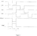
- Fig.4 is a view illustrating an operation timing of the light-emitting control circuit according to the second embodiment of the present disclosure, wherein the light-emitting control circuit is the first light-emitting control circuit stage in the shift register.
- a pulse width of the STV is twice as a pulse width of the CK1, a pulse width of the CK2 and a pulse width of the CK3.
- a first falling edge of the CK1 aligns with a falling edge of the STV; a first falling edge of the CK2 aligns with a first rising edge of the CK2; a first falling edge of the CK3 aligns with a rising edge of the STV; a duty ratios of the CK1, the CK2 and the CK3 are 1/3.
- a t1 stage is an input sampling stage.
- the input signal STV is also in the low level, and the CK1 is in the low level at this moment so the T1 is turned on, the CK3 is in the high level so the T8 is turned off, then the level at the N1 node is pulled down to VGL+
- the T10 and T11 are turned on, the N2 node and the N3 node are in the high level, and because the transistors T4 and T6 are turned off, the levels at the N3 node and the N5 node are ensured; on the other hand, the T13 is turned on, so the light-emitting control signal output from the outputting terminal EM[n] for the light-emitting control signal is in the low level; wherein Vthp is a threshold voltage of a p-type thin film transistor.
- a t2 stage is an outputting stage.
- the CK1 and CK3 are in the high level, the transistors T1, T3, T2 and T9 are all turned off, the level at the N1 node is pulled down correspondingly because of the bootstrap effect of the capacitor C1; the T3 is turned on, the CK2 signal is in the low level, the level at the N2 node is low at this time, then the T4 is turned on to pull down the level at the N3 node; accordingly, the T6 is turned on, the N5 node is in the high level and the T13 is turned off; the T7 is turned on since the CK2 is in the low level, so the light-emitting control signal output from the outputting terminal EM[n] for the light-emitting control signal is a high level signal and provides a ON signal to the OLED device.
- a t3 stage is a resetting stage.
- the CK3 is low, the T8 and T9 are turned on accordingly to pull up the level at the N1 node and pull down the level at the N4 node.
- the T12 is turned on, the level at the N5 node is in the low level.
- the T10 and T11 are turned on so as to pull up the levels at the N2 node and the N3 node.
- the T4 and T6 are turned off so that the levels at the N3 node and the N5 node are ensured; the T13 is turned on since the N5 node is in the low level, then the light-emitting control signal output from the outputting terminal EM[n] for the light-emitting control signal is pulled down again at this time, thus a resetting of the light-emitting control signal is achieved.
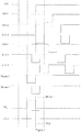
- Fig.5 is a view illustrating an operation timing of the shift register as shown in Fig.3 .
- EM_out_1, EM_out_2, EM_out_n denote an opposite phase outputting terminal of a first light-emitting control circuit stage, an opposite phase outputting terminal of a second light-emitting control circuit stage and an opposite phase outputting terminal of a nth light-emitting control circuit stage, respectively.
- EM_1, EM_2, EM_n denote the light-emitting control signal output from the first light-emitting control circuit stage, light-emitting control signal output from the second light-emitting control circuit stage and the light-emitting control signal output from the nth light-emitting control circuit stage, respectively.
- n is an integer being smaller than or equal to a number of stages of the light-emitting control circuits included in the shift register.
- a pulse width of CLK1-1, a pulse width of CLK1-2, a pulse width of CLK1-3, a pulse width of CLK2-1, a pulse width of CLK2-2 and a pulse width of CLK2-3 are same.
- a pulse width of the start signal STV is twice as the pulse width of CLK1-1, the pulse width of CLK1-2, the pulse width of CLK1-3, the pulse width of CLK2-1, the pulse width of CLK2-2 and the pulse width of CLK2-3, respectively.
- a first falling edge of the CLK1-1 aligns with a falling edge of the STV; a first falling edge of the CLK1-2 aligns with a first rising edge of the CLK1-1; a first falling edge of the CLK1-3 aligns with a rising edge of the STV; a first falling edge of the CLK2-1 locates at a 1/4 pulse width of the STV, that is, at a 1/2 pulse width of the CLK1-1 itself; a first falling edge of the CLK2-2 aligns with a first rising edge of the CLK2-1; a first falling edge of the CLK2-3 aligns with a first rising edge of the CLK2-2; a duty ratio of the CLK1-1, a duty ratio of the CLK1-2, a duty ratio of the CLK1-3, a duty ratio of the CLK2-1, a duty ratio of the CLK2-2 and a duty ratio of the CLK2-3 are 1/3.
- the embodiments of the present disclosure further provide a light-emitting control method for generating a light-emitting control signal which controls an OLED to emit light in an AMOLED, phases of the light-emitting control signal and a gate driving signal are opposite; the light-emitting control method comprises steps of:
- a resetting step in which a resetting unit resets the light-emitting control signal through the output pulling-down unit under a control of a third clock signal.
Landscapes
- Engineering & Computer Science (AREA)
- Microelectronics & Electronic Packaging (AREA)
- Physics & Mathematics (AREA)
- Computer Hardware Design (AREA)
- General Physics & Mathematics (AREA)
- Theoretical Computer Science (AREA)
- Power Engineering (AREA)
- Control Of Indicators Other Than Cathode Ray Tubes (AREA)
- Electroluminescent Light Sources (AREA)
Claims (7)
- Système comprenant un circuit d'attaque de grille apte à produire un signal d'attaque de grille et un circuit de commande d'émission de lumière apte à générer un signal de commande d'émission de lumière pour commander une diode électroluminescente organique, OLED, pour émettre une lumière dans une OLED à matrice active, AMOLED, le circuit de commande d'émission de lumière étant apte à produire un signal de commande d'émission de lumière en opposition de phase par rapport à la phase du circuit d'attaque de grille, le circuit de commande d'émission de lumière étant apte à être connecté à une borne de sortie de niveau bas (VGL) et une borne de sortie de niveau haut (VGH) d'une alimentation de puissance d'attaque ;
le circuit de commande d'émission de lumière comprend une borne d'entrée (Input), une unité d'échantillonnage d'entrée (11), une unité de sortie (12), une unité de réinitialisation (13), une unité de rappel vers le niveau bas de sortie (14), et une borne de sortie (EM[n]) pour le signal de commande d'émission de lumière, dans lequel
l'unité de rappel vers le niveau bas de sortie (14) est connectée à la borne de sortie (EM[n]) ;
l'unité d'échantillonnage d'entrée (11) est connectée respectivement à la borne d'entrée (Input), une borne d'entrée de premier signal d'horloge (CK1) et à l'unité de rappel vers le niveau bas de sortie (14), et est apte à échantillonner un signal d'entrée reçu sur la borne d'entrée (Input) sous le contrôle d'un premier signal d'horloge reçu sur la borne d'entrée de premier signal d'horloge (CK1), et à transmettre le signal échantillonné à la borne de sortie (EM[n]) pour le signal de commande d'émission de lumière par le biais de l'unité de rappel vers le niveau bas de sortie (14) ;
l'unité de sortie (12) est connectée respectivement à l'unité d'échantillonnage d'entrée, une borne d'entrée (11) de deuxième signal d'horloge (CK2), et la borne de sortie (EM[n]), et est apte à générer le signal de commande d'émission de lumière sous le contrôle d'un deuxième signal d'horloge reçu sur la borne d'entrée de deuxième signal d'horloge (CK2) après échantillonnage par l'unité d'échantillonnage d'entrée (11) du signal d'entrée, et à transmettre le signal de commande d'émission de lumière à la borne de sortie (EM[n]) pour le signal de commande d'émission de lumière ;
l'unité de réinitialisation (13) est connectée respectivement à une borne d'entrée de troisième signal d'horloge (CK3) et à l'unité de rappel vers le niveau bas de sortie (14), et est apte à envoyer un signal de commande de réinitialisation à l'unité de rappel vers le niveau bas de sortie (14) sous le contrôle d'un troisième signal d'horloge reçu sur la borne d'entrée de troisième signal d'horloge (CK3) ;
l'unité de rappel vers le niveau bas de sortie (14) est apte à réinitialiser le signal de commande d'émission de lumière en fonction du signal de commande de réinitialisation ;
l'unité d'échantillonnage d'entrée (11) comprend un premier transistor à couches minces (T1) et un deuxième transistor à couches minces (T2) ;
une grille du premier transistor à couches minces (T1) est connectée à la borne d'entrée de premier signal d'horloge (CK1), une source de celui-ci est connectée à l'unité de sortie (12), et un drain de celui-ci est connecté à la borne d'entrée (Input) ;
une grille du deuxième transistor à couches minces (T2) est connectée à la borne d'entrée de premier signal d'horloge (CK1), une source de celui-ci est connectée à l'unité de sortie (12), et un drain de celui-ci est connectée à la borne de sortie de niveau bas (VGL) de l'alimentation de puissance d'attaque ;
l'unité de rappel vers le niveau bas de sortie (14) comprend un douzième transistor à couches minces (T12), une grille de celui-ci est connectée à la source du deuxième transistor à couches minces (T2), un drain de celui-ci est connecté à la borne de sortie de niveau bas (VGL) de l'alimentation de puissance d'attaque ;
l'unité de sortie (12) comprend un troisième transistor à couches minces (T3), un quatrième transistor à couches minces (T4), un cinquième transistor à couches minces (T5), un sixième transistor à couches minces (T6), un premier condensateur (C1), et un deuxième condensateur (C2) ;
une grille du troisième transistor à couches minces (T3) est connectée à la source du premier transistor à couches minces (T1), une source de celui-ci est connectée à une grille du quatrième transistor à couches minces (T4), et un drain de celui-ci est connectée à la borne d'entrée de deuxième signal d'horloge (CK2) ;
une source du quatrième transistor à couches minces (T4) est connectée à une grille du sixième transistor à couches minces (T6), et un drain de celui-ci est connecté à la borne de sortie de niveau bas (VGL) de l'alimentation de puissance d'attaque ;
une source du cinquième transistor à couches minces (T5) est connectée à la borne de sortie de niveau haut (VGH) de l'alimentation de puissance d'attaque, et un drain de celui-ci est connecté à la source du deuxième transistor à couches minces (T2) ;
la source du sixième transistor à couches minces (T6) est connectée à la borne de sortie de niveau haut (VGH) de l'alimentation de puissance d'attaque, et un drain de celui-ci est connecté à une source du douzième transistor à couches minces (T12) ;
le premier condensateur (C1) est connecté entre la grille et la source du troisième transistor à couches minces (T3) ;
le système étant caractérisé en ce que :l'unité de rappel vers le niveau bas de sortie (14) comprend en outre un treizième transistor à couches minces (T13) et un quatrième condensateur (C4), dans lequel une source du treizième transistor à couches minces (T13) est connectée à la borne de sortie (EM[n]), une grille de celui-ci est connectée à la source du douzième transistor à couches minces (T12), et un drain de celui-ci est connecté à la borne de sortie de niveau bas (VGL) de l'alimentation de puissance d'attaque, et dans lequel le quatrième condensateur (C4) est connecté à la grille et à la source du treizième transistor à couches minces (T13), etl'unité de sortie (12) comprend en outre un deuxième condensateur (C2) et un septième transistor à couches minces (T7), dans lequel une grille de celui-ci est connectée à la borne d'entrée de deuxième signal d'horloge (CK2), une source de celui-ci est connectée à la borne de sortie de niveau haut (VGH) de l'alimentation de puissance d'attaque, et un drain de celui-ci est connecté à une source d'un treizième transistor à couches minces (T13), dans lequel une grille du cinquième transistor à couches minces (T5) est connectée à la borne d'entrée de deuxième signal d'horloge (CK2), et dans lequel le deuxième condensateur (C2) est connecté entre la grille du sixième transistor à couches minces (T6) et la borne de sortie de niveau bas (VGL) de l'alimentation de puissance d'attaque. - Système selon la revendication 1, dans lequel
l'unité de réinitialisation (13) comprend un huitième transistor à couches minces (T8) et un neuvième transistor à couches minces (T9) ;
une grille du huitième transistor à couches minces (T8) est connectée à la borne d'entrée de troisième signal d'horloge (CK3), une source de celui-ci est connectée à la borne de sortie de niveau haut (VGH) de l'alimentation de puissance d'attaque, et un drain de celui-ci est connecté à la source du premier transistor à couches minces (T1), et
une grille du neuvième transistor à couches minces (T9) est connectée à la borne d'entrée de troisième signal d'horloge (CK3), une source de celui-ci est connectée à la source du deuxième transistor à couches minces (T2), et un drain de celui-ci est connecté à la borne de sortie de niveau bas (VGL) de l'alimentation de puissance d'attaque. - Système selon la revendication 2, dans lequel
l'unité de rappel vers le niveau bas de sortie (14) comprend en outre un dixième transistor à couches minces (10), un onzième transistor à couches minces (11), un troisième condensateur (C3), un cinquième condensateur (C5), et un sixième condensateur (C6) ;
une grille du dixième transistor à couches minces (T10) est connectée à une grille du onzième transistor à couches minces (T11), une source de celui-ci est connectée à la borne de sortie de niveau haut (VGH) de l'alimentation de puissance d'attaque, et un drain de celui-ci est connecté à la source du troisième transistor à couches minces (T3) ;
une source du onzième transistor à couches minces (T11) est connectée à la borne de sortie de niveau haut (VGH) de l'alimentation de puissance d'attaque, et un drain de celui-ci est connecté à la source du quatrième transistor à couches minces (T4) ; une grille du treizième transistor à couches minces (T13) est connectée à la grille du dixième transistor à couches minces (T10) ;
le troisième condensateur (C3) est connecté entre la grille et la source du douzième transistor à couches minces (T12) ;
le cinquième condensateur (C5) est connecté entre la grille du dixième transistor à couches minces (T10) et la borne de sortie de niveau bas (VGL) de l'alimentation de puissance d'attaque ;
le sixième condensateur (C6) est connecté entre la borne de sortie (EM[n]) et la borne de sortie de niveau bas (VGL) de l'alimentation de puissance d'attaque. - Système selon la revendication 3, dans lequel
le circuit de commande d'émission de lumière comprend en outre une borne de sortie en opposition de phase (EM_out) ;
la grille du quatrième transistor à couches minces (T4) est connectée à la borne de sortie en opposition de phase (EM_out), et
un signal produit à partir de la borne de sortie en opposition de phase (EM_out) présente une opposition de phase avec le signal de commande d'émission de lumière. - Système selon la revendication 3 ou 4, dans lequel le premier transistor à couches minces (T1), le deuxième transistor à couches minces (T2), le troisième transistor à couches minces (T3), le quatrième transistor à couches minces (T4), le cinquième transistor à couches minces (T5), le sixième transistor à couches minces (T6), le septième transistor à couches minces (T7), le huitième transistor à couches minces (T8), le neuvième transistor à couches minces (T9), le dixième transistor à couches minces (T10), le onzième transistor à couches minces (T11), le douzième transistor à couches minces (T12), et le treizième transistor à couches minces (T13) sont transistors à couches minces (TFT) de type p.
- Procédé de commande d'émission de lumière destiné à commander le système selon l'une quelconque des revendications 1 à 5, destiné à générer le signal de commande d'émission de lumière pour commander une diode électroluminescente organique, OLED, pour émettre une lumière dans une OLED à matrice active, AMOLED, dans lequel la phase du signal de commande d'émission de lumière présente une opposition de phase par rapport au signal d'attaque de grille produit par le circuit d'attaque de grille ;
le procédé de commande d'émission de lumière comprenant les étapes suivantes :une étape d'échantillonnage d'entrée, où l'unité d'échantillonnage d'entrée (11) échantillonne le signal d'entrée sous le contrôle d'un premier signal d'horloge (CK1), et transmet le signal échantillonné à la borne de sortie (EM[n]) pour le signal de commande d'émission de lumière par le biais de l'unité de rappel vers le niveau bas de sortie (14) ;une étape de sortie, où l'unité de sortie (12) génère le signal de commande d'émission de lumière sous le contrôle d'un deuxième signal d'horloge (CK2) après échantillonnage par l'unité d'échantillonnage d'entrée (11) du signal d'entrée, et transmet le signal de commande d'émission de lumière à la borne de sortie (EM[n]) pour le signal de commande d'émission de lumière ;une étape de réinitialisation, où l'unité de réinitialisation (13) réinitialise le signal de commande d'émission de lumière par le biais de l'unité de rappel vers le niveau bas de sortie (14) sous le contrôle du troisième signal d'horloge (CK3). - Système selon l'une quelconque des revendications 1 à 5, comprenant en outre un registre à décalage comprenant une pluralité de circuits de commande d'émission de lumière, dans lequel
excepté pour le premier étage de circuit de commande d'émission de lumière (STAGE_1) et le deuxième étage de circuit de commande d'émission de lumière (STAGE_2), un signal d'entrée (Input) du nième étage de circuit de commande d'émission de lumière (STAGE_3, STAGE_4, STAGE_5, STAGE_6, ...) est un signal présentant une opposition de phase par rapport à celle d'un signal de commande d'émission de lumière d'un (n-2)ième étage de circuit de commande d'émission de lumière ;
un signal d'entrée du premier étage de circuit de commande d'émission de lumière (STAGE_1) et un signal d'entrée du deuxième étage de circuit de commande d'émission de lumière (STAGE_2) sont un signal de lancement (STV), et
n est un entier supérieur à 2 et inférieur ou égal à N, N étant un nombre d'étages des circuits de commande d'émission de lumière inclus dans le registre à décalage.
Applications Claiming Priority (2)
| Application Number | Priority Date | Filing Date | Title |
|---|---|---|---|
| CN201210244368.3A CN102760406B (zh) | 2012-07-13 | 2012-07-13 | 发光控制电路、发光控制方法和移位寄存器 |
| PCT/CN2012/084973 WO2014008732A1 (fr) | 2012-07-13 | 2012-11-21 | Circuit de commande d'émission de lumière, procédé de commande d'émission de lumière et registre à décalage |
Publications (3)
| Publication Number | Publication Date |
|---|---|
| EP2874140A1 EP2874140A1 (fr) | 2015-05-20 |
| EP2874140A4 EP2874140A4 (fr) | 2016-03-09 |
| EP2874140B1 true EP2874140B1 (fr) | 2018-04-04 |
Family
ID=47054853
Family Applications (1)
| Application Number | Title | Priority Date | Filing Date |
|---|---|---|---|
| EP12880722.9A Active EP2874140B1 (fr) | 2012-07-13 | 2012-11-21 | Circuit de commande d'émission de lumière, procédé de commande d'émission de lumière et registre à décalage |
Country Status (4)
| Country | Link |
|---|---|
| US (1) | US9113534B2 (fr) |
| EP (1) | EP2874140B1 (fr) |
| CN (1) | CN102760406B (fr) |
| WO (1) | WO2014008732A1 (fr) |
Cited By (1)
| Publication number | Priority date | Publication date | Assignee | Title |
|---|---|---|---|---|
| US11151946B2 (en) | 2019-01-04 | 2021-10-19 | Boe Technology Group Co., Ltd. | Shift register unit and driving method, gate driving circuit, and display device |
Families Citing this family (31)
| Publication number | Priority date | Publication date | Assignee | Title |
|---|---|---|---|---|
| CN102760406B (zh) | 2012-07-13 | 2015-01-28 | 京东方科技集团股份有限公司 | 发光控制电路、发光控制方法和移位寄存器 |
| CN102760407B (zh) * | 2012-07-13 | 2015-11-25 | 京东方科技集团股份有限公司 | 发光控制电路、发光控制方法和移位寄存器 |
| CN103065584B (zh) * | 2012-12-18 | 2015-06-03 | 华南理工大学 | 有源有机电致发光显示器扫描驱动器及其驱动方法 |
| CN103886910B (zh) * | 2012-12-19 | 2017-07-11 | 群康科技(深圳)有限公司 | 移位暂存器 |
| TWI595472B (zh) | 2014-06-23 | 2017-08-11 | 友達光電股份有限公司 | 顯示面板 |
| CN104157236B (zh) * | 2014-07-16 | 2016-05-11 | 京东方科技集团股份有限公司 | 一种移位寄存器及栅极驱动电路 |
| TWI546786B (zh) * | 2014-08-22 | 2016-08-21 | 友達光電股份有限公司 | 顯示面板 |
| CN104821148B (zh) * | 2015-05-28 | 2016-11-09 | 京东方科技集团股份有限公司 | 移位寄存器单元、驱动方法、栅极驱动电路和显示装置 |
| CN104821153B (zh) * | 2015-05-29 | 2017-06-16 | 京东方科技集团股份有限公司 | 栅极驱动电路及oled显示装置 |
| KR102413874B1 (ko) * | 2015-07-02 | 2022-06-29 | 삼성디스플레이 주식회사 | 발광제어 구동부 및 이를 포함하는 표시장치 |
| CN105632560B (zh) * | 2016-01-04 | 2019-08-02 | 京东方科技集团股份有限公司 | 移位寄存器单元、驱动方法、栅极驱动电路及显示装置 |
| CN105609054B (zh) * | 2016-02-29 | 2018-05-08 | 信利(惠州)智能显示有限公司 | 一种发光控制电路及移位寄存器 |
| CN105632410B (zh) * | 2016-03-15 | 2018-04-10 | 上海天马有机发光显示技术有限公司 | 一种移位寄存器、栅极驱动电路、显示面板以及驱动方法 |
| US10492257B2 (en) * | 2016-05-20 | 2019-11-26 | Panasonic Intellectual Property Management Co., Ltd. | Lighting device and lighting fixture |
| CN108417183B (zh) * | 2017-02-10 | 2020-07-03 | 京东方科技集团股份有限公司 | 移位寄存器及其驱动方法、栅极驱动电路、显示装置 |
| CN108665853B (zh) * | 2017-03-27 | 2020-11-13 | 昆山工研院新型平板显示技术中心有限公司 | 控制信号驱动电路与驱动方法以及像素电路驱动方法 |
| CN108806588B (zh) * | 2017-04-28 | 2020-06-12 | 昆山国显光电有限公司 | 一种发光控制电路、发光控制方法以及移位寄存器 |
| CN107093393A (zh) * | 2017-07-03 | 2017-08-25 | 成都晶砂科技有限公司 | 栅极驱动电路和发光控制驱动电路相融合的驱动电路 |
| CN108039150B (zh) * | 2017-11-16 | 2020-05-19 | 武汉华星光电半导体显示技术有限公司 | 移位寄存电路及移位寄存单元 |
| CN108806583B (zh) * | 2018-07-05 | 2020-12-01 | 京东方科技集团股份有限公司 | 移位寄存器单元、驱动方法、移位寄存器和显示装置 |
| CN108682398B (zh) | 2018-08-08 | 2020-05-29 | 京东方科技集团股份有限公司 | 移位寄存器单元、栅极驱动电路、显示装置及驱动方法 |
| CN110072320B (zh) * | 2019-06-04 | 2024-03-29 | 沈阳乐节科技有限公司 | 一种汽车用动态显示灯控制电路 |
| KR102669165B1 (ko) * | 2019-11-05 | 2024-05-28 | 삼성디스플레이 주식회사 | 발광 제어 구동부 및 이를 포함하는 표시 장치 |
| CN113096607A (zh) * | 2019-12-23 | 2021-07-09 | 深圳市柔宇科技股份有限公司 | 像素扫描驱动电路、阵列基板与显示终端 |
| CN111179805B (zh) * | 2020-01-16 | 2023-02-17 | 京东方科技集团股份有限公司 | 移位寄存器单元及其驱动方法、栅极驱动电路、显示面板 |
| CN114882831A (zh) | 2022-05-13 | 2022-08-09 | 武汉华星光电半导体显示技术有限公司 | 一种显示面板的显示控制方法、显示模组及显示装置 |
| CN114927089B (zh) * | 2022-05-20 | 2024-03-05 | 京东方科技集团股份有限公司 | 一种驱动电路、显示面板及电子设备 |
| CN115206239B (zh) | 2022-06-30 | 2024-09-24 | 厦门天马显示科技有限公司 | 显示面板及其显示驱动方法、显示装置 |
| US12573340B2 (en) | 2022-07-29 | 2026-03-10 | Hefei Boe Joint Technology Co., Ltd. | Driving signal generation circuit, method, module and display device |
| CN115346487B (zh) * | 2022-09-02 | 2024-12-24 | 武汉天马微电子有限公司 | 显示面板及其驱动方法、显示装置 |
| CN116092444B (zh) * | 2023-02-23 | 2026-02-17 | 重庆京东方光电科技有限公司 | 栅极驱动电路及其驱动方法、显示面板 |
Family Cites Families (15)
| Publication number | Priority date | Publication date | Assignee | Title |
|---|---|---|---|---|
| KR100646992B1 (ko) * | 2005-09-13 | 2006-11-23 | 삼성에스디아이 주식회사 | 발광제어선 구동부 및 이를 이용한 유기 발광 표시장치 |
| KR100732809B1 (ko) * | 2005-11-03 | 2007-06-27 | 삼성에스디아이 주식회사 | 데이터 구동부 및 이를 이용한 유기 발광표시장치 |
| KR100748334B1 (ko) * | 2006-05-09 | 2007-08-09 | 삼성에스디아이 주식회사 | 데이터 구동부 및 이를 이용한 유기 전계 발광 표시장치 |
| US20100188385A1 (en) | 2007-07-24 | 2010-07-29 | Koninklijke Philips Electronics N.V. | Shift register circuit having threshold voltage compensation |
| TWI398852B (zh) * | 2008-06-06 | 2013-06-11 | Au Optronics Corp | 可降低時脈偶合效應之移位暫存器及移位暫存器單元 |
| KR101022173B1 (ko) * | 2009-01-13 | 2011-03-17 | 삼성모바일디스플레이주식회사 | 쉬프트 레지스터 및 이를 이용한 유기전계발광 표시장치 |
| KR101350635B1 (ko) * | 2009-07-03 | 2014-01-10 | 엘지디스플레이 주식회사 | 듀얼 쉬프트 레지스터 |
| TWI382669B (zh) * | 2009-07-16 | 2013-01-11 | Ralink Technology Corp | 用於管線式類比數位轉換器之比較器及相關訊號取樣方法 |
| CN101697284B (zh) * | 2009-08-24 | 2013-08-07 | 友达光电股份有限公司 | 移位寄存器电路 |
| KR101056434B1 (ko) * | 2010-02-05 | 2011-08-11 | 삼성모바일디스플레이주식회사 | 표시 장치 및 그 구동 방법 |
| KR101944465B1 (ko) | 2011-01-06 | 2019-02-07 | 삼성디스플레이 주식회사 | 발광 제어선 구동부 및 이를 이용한 유기전계발광 표시장치 |
| TWI493557B (zh) * | 2011-04-28 | 2015-07-21 | Au Optronics Corp | 移位暫存器電路 |
| CN102650492A (zh) * | 2012-05-10 | 2012-08-29 | 西安交通大学 | 空分板翅型降膜式冷凝蒸发器 |
| CN102760406B (zh) | 2012-07-13 | 2015-01-28 | 京东方科技集团股份有限公司 | 发光控制电路、发光控制方法和移位寄存器 |
| CN202650492U (zh) * | 2012-07-13 | 2013-01-02 | 京东方科技集团股份有限公司 | 发光控制电路和移位寄存器 |
-
2012
- 2012-07-13 CN CN201210244368.3A patent/CN102760406B/zh active Active
- 2012-11-21 US US14/126,640 patent/US9113534B2/en active Active
- 2012-11-21 EP EP12880722.9A patent/EP2874140B1/fr active Active
- 2012-11-21 WO PCT/CN2012/084973 patent/WO2014008732A1/fr not_active Ceased
Non-Patent Citations (1)
| Title |
|---|
| None * |
Cited By (2)
| Publication number | Priority date | Publication date | Assignee | Title |
|---|---|---|---|---|
| US11151946B2 (en) | 2019-01-04 | 2021-10-19 | Boe Technology Group Co., Ltd. | Shift register unit and driving method, gate driving circuit, and display device |
| US11688351B2 (en) | 2019-01-04 | 2023-06-27 | Boe Technology Group Co., Ltd. | Shift register unit and driving method, gate driving circuit, and display device |
Also Published As
| Publication number | Publication date |
|---|---|
| CN102760406B (zh) | 2015-01-28 |
| EP2874140A4 (fr) | 2016-03-09 |
| US9113534B2 (en) | 2015-08-18 |
| CN102760406A (zh) | 2012-10-31 |
| WO2014008732A1 (fr) | 2014-01-16 |
| US20140285108A1 (en) | 2014-09-25 |
| EP2874140A1 (fr) | 2015-05-20 |
Similar Documents
| Publication | Publication Date | Title |
|---|---|---|
| EP2874140B1 (fr) | Circuit de commande d'émission de lumière, procédé de commande d'émission de lumière et registre à décalage | |
| EP3223268B1 (fr) | Unité de registre de décalage et son procédé d'actionnement, registre de décalage et dispositif d'affichage | |
| EP2672479B1 (fr) | Unité de commande de grille sur réseau, circuit de commande de grille sur réseau et dispositif d'affichage | |
| US9881543B2 (en) | Shift register unit, method for driving the same, shift register, and display device | |
| US9620241B2 (en) | Shift register unit, method for driving the same, shift register and display device | |
| CN102779478B (zh) | 移位寄存器单元及其驱动方法、移位寄存器和显示装置 | |
| CN104835450B (zh) | 移位寄存器单元及其控制方法、栅极驱动电路、显示装置 | |
| CN105609041B (zh) | 移位寄存器单元及其驱动方法、栅极驱动电路、显示装置 | |
| CN105702295B (zh) | 移位寄存器单元、栅极驱动电路、显示面板及显示装置 | |
| CN102760407B (zh) | 发光控制电路、发光控制方法和移位寄存器 | |
| WO2017185590A1 (fr) | Unité de registre à décalage, circuit de pilotage de grille et procédé de pilotage pour celui-ci, et dispositif d'affichage | |
| US20160314850A1 (en) | Shift register unit, method for driving the same, gate driver circuit and display device | |
| US10146362B2 (en) | Shift register unit, a shift register, a driving method, and an array substrate | |
| CN104978922B (zh) | 移位寄存器、显示装置及移位寄存器驱动方法 | |
| US20160172054A1 (en) | Shift register unit, its driving method, shift register and display device | |
| US9991005B2 (en) | Shift register and driving method thereof | |
| EP3232430A1 (fr) | Registre à décalage et procédé de commande associé, circuit de balayage à décalage et dispositif d'affichage | |
| CN105139825B (zh) | 移位寄存器单元、栅极驱动装置、显示装置、控制方法 | |
| EP3067878A1 (fr) | Circuit d'attaque de balayage et dispositif d'affichage électroluminescent organique l'utilisant | |
| EP3657485A1 (fr) | Unité de registre à décalage et son procédé d'attaque et circuit d'attaque de grille | |
| CN104464628A (zh) | 移位寄存器单元及驱动方法、栅极驱动电路及显示装置 | |
| US10204579B2 (en) | GOA circuits, display devices and the driving methods of the GOA circuits | |
| KR20170126567A (ko) | 표시 패널 구동부 및 이를 포함하는 표시 장치 | |
| US20170301277A1 (en) | Gate on array (goa) unit, gate driver circuit and display device | |
| CN103559913A (zh) | 一种移位寄存器 |
Legal Events
| Date | Code | Title | Description |
|---|---|---|---|
| PUAI | Public reference made under article 153(3) epc to a published international application that has entered the european phase |
Free format text: ORIGINAL CODE: 0009012 |
|
| 17P | Request for examination filed |
Effective date: 20140114 |
|
| AK | Designated contracting states |
Kind code of ref document: A1 Designated state(s): AL AT BE BG CH CY CZ DE DK EE ES FI FR GB GR HR HU IE IS IT LI LT LU LV MC MK MT NL NO PL PT RO RS SE SI SK SM TR |
|
| AX | Request for extension of the european patent |
Extension state: BA ME |
|
| DAX | Request for extension of the european patent (deleted) | ||
| RA4 | Supplementary search report drawn up and despatched (corrected) |
Effective date: 20160204 |
|
| RIC1 | Information provided on ipc code assigned before grant |
Ipc: G11C 19/28 20060101ALI20160129BHEP Ipc: G09G 3/32 20060101AFI20160129BHEP |
|
| STAA | Information on the status of an ep patent application or granted ep patent |
Free format text: STATUS: EXAMINATION IS IN PROGRESS |
|
| 17Q | First examination report despatched |
Effective date: 20161202 |
|
| REG | Reference to a national code |
Ref country code: DE Ref legal event code: R079 Ref document number: 602012044923 Country of ref document: DE Free format text: PREVIOUS MAIN CLASS: G09G0003320000 Ipc: G09G0003326600 |
|
| RIC1 | Information provided on ipc code assigned before grant |
Ipc: G09G 3/3266 20160101AFI20171005BHEP Ipc: G11C 19/28 20060101ALN20171005BHEP |
|
| GRAP | Despatch of communication of intention to grant a patent |
Free format text: ORIGINAL CODE: EPIDOSNIGR1 |
|
| STAA | Information on the status of an ep patent application or granted ep patent |
Free format text: STATUS: GRANT OF PATENT IS INTENDED |
|
| INTG | Intention to grant announced |
Effective date: 20171113 |
|
| GRAS | Grant fee paid |
Free format text: ORIGINAL CODE: EPIDOSNIGR3 |
|
| GRAA | (expected) grant |
Free format text: ORIGINAL CODE: 0009210 |
|
| STAA | Information on the status of an ep patent application or granted ep patent |
Free format text: STATUS: THE PATENT HAS BEEN GRANTED |
|
| AK | Designated contracting states |
Kind code of ref document: B1 Designated state(s): AL AT BE BG CH CY CZ DE DK EE ES FI FR GB GR HR HU IE IS IT LI LT LU LV MC MK MT NL NO PL PT RO RS SE SI SK SM TR |
|
| REG | Reference to a national code |
Ref country code: GB Ref legal event code: FG4D |
|
| REG | Reference to a national code |
Ref country code: CH Ref legal event code: EP |
|
| REG | Reference to a national code |
Ref country code: AT Ref legal event code: REF Ref document number: 986395 Country of ref document: AT Kind code of ref document: T Effective date: 20180415 |
|
| REG | Reference to a national code |
Ref country code: IE Ref legal event code: FG4D |
|
| REG | Reference to a national code |
Ref country code: DE Ref legal event code: R096 Ref document number: 602012044923 Country of ref document: DE |
|
| REG | Reference to a national code |
Ref country code: NL Ref legal event code: FP |
|
| REG | Reference to a national code |
Ref country code: LT Ref legal event code: MG4D |
|
| REG | Reference to a national code |
Ref country code: FR Ref legal event code: PLFP Year of fee payment: 7 |
|
| PG25 | Lapsed in a contracting state [announced via postgrant information from national office to epo] |
Ref country code: BG Free format text: LAPSE BECAUSE OF FAILURE TO SUBMIT A TRANSLATION OF THE DESCRIPTION OR TO PAY THE FEE WITHIN THE PRESCRIBED TIME-LIMIT Effective date: 20180704 Ref country code: ES Free format text: LAPSE BECAUSE OF FAILURE TO SUBMIT A TRANSLATION OF THE DESCRIPTION OR TO PAY THE FEE WITHIN THE PRESCRIBED TIME-LIMIT Effective date: 20180404 Ref country code: LT Free format text: LAPSE BECAUSE OF FAILURE TO SUBMIT A TRANSLATION OF THE DESCRIPTION OR TO PAY THE FEE WITHIN THE PRESCRIBED TIME-LIMIT Effective date: 20180404 Ref country code: PL Free format text: LAPSE BECAUSE OF FAILURE TO SUBMIT A TRANSLATION OF THE DESCRIPTION OR TO PAY THE FEE WITHIN THE PRESCRIBED TIME-LIMIT Effective date: 20180404 Ref country code: NO Free format text: LAPSE BECAUSE OF FAILURE TO SUBMIT A TRANSLATION OF THE DESCRIPTION OR TO PAY THE FEE WITHIN THE PRESCRIBED TIME-LIMIT Effective date: 20180704 Ref country code: FI Free format text: LAPSE BECAUSE OF FAILURE TO SUBMIT A TRANSLATION OF THE DESCRIPTION OR TO PAY THE FEE WITHIN THE PRESCRIBED TIME-LIMIT Effective date: 20180404 Ref country code: SE Free format text: LAPSE BECAUSE OF FAILURE TO SUBMIT A TRANSLATION OF THE DESCRIPTION OR TO PAY THE FEE WITHIN THE PRESCRIBED TIME-LIMIT Effective date: 20180404 Ref country code: AL Free format text: LAPSE BECAUSE OF FAILURE TO SUBMIT A TRANSLATION OF THE DESCRIPTION OR TO PAY THE FEE WITHIN THE PRESCRIBED TIME-LIMIT Effective date: 20180404 |
|
| PG25 | Lapsed in a contracting state [announced via postgrant information from national office to epo] |
Ref country code: RS Free format text: LAPSE BECAUSE OF FAILURE TO SUBMIT A TRANSLATION OF THE DESCRIPTION OR TO PAY THE FEE WITHIN THE PRESCRIBED TIME-LIMIT Effective date: 20180404 Ref country code: HR Free format text: LAPSE BECAUSE OF FAILURE TO SUBMIT A TRANSLATION OF THE DESCRIPTION OR TO PAY THE FEE WITHIN THE PRESCRIBED TIME-LIMIT Effective date: 20180404 Ref country code: GR Free format text: LAPSE BECAUSE OF FAILURE TO SUBMIT A TRANSLATION OF THE DESCRIPTION OR TO PAY THE FEE WITHIN THE PRESCRIBED TIME-LIMIT Effective date: 20180705 Ref country code: LV Free format text: LAPSE BECAUSE OF FAILURE TO SUBMIT A TRANSLATION OF THE DESCRIPTION OR TO PAY THE FEE WITHIN THE PRESCRIBED TIME-LIMIT Effective date: 20180404 |
|
| REG | Reference to a national code |
Ref country code: AT Ref legal event code: MK05 Ref document number: 986395 Country of ref document: AT Kind code of ref document: T Effective date: 20180404 |
|
| PG25 | Lapsed in a contracting state [announced via postgrant information from national office to epo] |
Ref country code: PT Free format text: LAPSE BECAUSE OF FAILURE TO SUBMIT A TRANSLATION OF THE DESCRIPTION OR TO PAY THE FEE WITHIN THE PRESCRIBED TIME-LIMIT Effective date: 20180806 |
|
| REG | Reference to a national code |
Ref country code: DE Ref legal event code: R097 Ref document number: 602012044923 Country of ref document: DE |
|
| PG25 | Lapsed in a contracting state [announced via postgrant information from national office to epo] |
Ref country code: SK Free format text: LAPSE BECAUSE OF FAILURE TO SUBMIT A TRANSLATION OF THE DESCRIPTION OR TO PAY THE FEE WITHIN THE PRESCRIBED TIME-LIMIT Effective date: 20180404 Ref country code: RO Free format text: LAPSE BECAUSE OF FAILURE TO SUBMIT A TRANSLATION OF THE DESCRIPTION OR TO PAY THE FEE WITHIN THE PRESCRIBED TIME-LIMIT Effective date: 20180404 Ref country code: CZ Free format text: LAPSE BECAUSE OF FAILURE TO SUBMIT A TRANSLATION OF THE DESCRIPTION OR TO PAY THE FEE WITHIN THE PRESCRIBED TIME-LIMIT Effective date: 20180404 Ref country code: DK Free format text: LAPSE BECAUSE OF FAILURE TO SUBMIT A TRANSLATION OF THE DESCRIPTION OR TO PAY THE FEE WITHIN THE PRESCRIBED TIME-LIMIT Effective date: 20180404 Ref country code: EE Free format text: LAPSE BECAUSE OF FAILURE TO SUBMIT A TRANSLATION OF THE DESCRIPTION OR TO PAY THE FEE WITHIN THE PRESCRIBED TIME-LIMIT Effective date: 20180404 Ref country code: AT Free format text: LAPSE BECAUSE OF FAILURE TO SUBMIT A TRANSLATION OF THE DESCRIPTION OR TO PAY THE FEE WITHIN THE PRESCRIBED TIME-LIMIT Effective date: 20180404 |
|
| PLBE | No opposition filed within time limit |
Free format text: ORIGINAL CODE: 0009261 |
|
| STAA | Information on the status of an ep patent application or granted ep patent |
Free format text: STATUS: NO OPPOSITION FILED WITHIN TIME LIMIT |
|
| PG25 | Lapsed in a contracting state [announced via postgrant information from national office to epo] |
Ref country code: SM Free format text: LAPSE BECAUSE OF FAILURE TO SUBMIT A TRANSLATION OF THE DESCRIPTION OR TO PAY THE FEE WITHIN THE PRESCRIBED TIME-LIMIT Effective date: 20180404 Ref country code: IT Free format text: LAPSE BECAUSE OF FAILURE TO SUBMIT A TRANSLATION OF THE DESCRIPTION OR TO PAY THE FEE WITHIN THE PRESCRIBED TIME-LIMIT Effective date: 20180404 |
|
| 26N | No opposition filed |
Effective date: 20190107 |
|
| PG25 | Lapsed in a contracting state [announced via postgrant information from national office to epo] |
Ref country code: SI Free format text: LAPSE BECAUSE OF FAILURE TO SUBMIT A TRANSLATION OF THE DESCRIPTION OR TO PAY THE FEE WITHIN THE PRESCRIBED TIME-LIMIT Effective date: 20180404 |
|
| REG | Reference to a national code |
Ref country code: CH Ref legal event code: PL |
|
| PG25 | Lapsed in a contracting state [announced via postgrant information from national office to epo] |
Ref country code: LU Free format text: LAPSE BECAUSE OF NON-PAYMENT OF DUE FEES Effective date: 20181121 Ref country code: MC Free format text: LAPSE BECAUSE OF FAILURE TO SUBMIT A TRANSLATION OF THE DESCRIPTION OR TO PAY THE FEE WITHIN THE PRESCRIBED TIME-LIMIT Effective date: 20180404 |
|
| REG | Reference to a national code |
Ref country code: BE Ref legal event code: MM Effective date: 20181130 |
|
| REG | Reference to a national code |
Ref country code: IE Ref legal event code: MM4A |
|
| PG25 | Lapsed in a contracting state [announced via postgrant information from national office to epo] |
Ref country code: LI Free format text: LAPSE BECAUSE OF NON-PAYMENT OF DUE FEES Effective date: 20181130 Ref country code: CH Free format text: LAPSE BECAUSE OF NON-PAYMENT OF DUE FEES Effective date: 20181130 |
|
| PG25 | Lapsed in a contracting state [announced via postgrant information from national office to epo] |
Ref country code: IE Free format text: LAPSE BECAUSE OF NON-PAYMENT OF DUE FEES Effective date: 20181121 |
|
| PG25 | Lapsed in a contracting state [announced via postgrant information from national office to epo] |
Ref country code: BE Free format text: LAPSE BECAUSE OF NON-PAYMENT OF DUE FEES Effective date: 20181130 |
|
| PG25 | Lapsed in a contracting state [announced via postgrant information from national office to epo] |
Ref country code: MT Free format text: LAPSE BECAUSE OF NON-PAYMENT OF DUE FEES Effective date: 20181121 |
|
| PG25 | Lapsed in a contracting state [announced via postgrant information from national office to epo] |
Ref country code: TR Free format text: LAPSE BECAUSE OF FAILURE TO SUBMIT A TRANSLATION OF THE DESCRIPTION OR TO PAY THE FEE WITHIN THE PRESCRIBED TIME-LIMIT Effective date: 20180404 |
|
| PG25 | Lapsed in a contracting state [announced via postgrant information from national office to epo] |
Ref country code: HU Free format text: LAPSE BECAUSE OF FAILURE TO SUBMIT A TRANSLATION OF THE DESCRIPTION OR TO PAY THE FEE WITHIN THE PRESCRIBED TIME-LIMIT; INVALID AB INITIO Effective date: 20121121 Ref country code: MK Free format text: LAPSE BECAUSE OF NON-PAYMENT OF DUE FEES Effective date: 20180404 Ref country code: CY Free format text: LAPSE BECAUSE OF FAILURE TO SUBMIT A TRANSLATION OF THE DESCRIPTION OR TO PAY THE FEE WITHIN THE PRESCRIBED TIME-LIMIT Effective date: 20180404 |
|
| PG25 | Lapsed in a contracting state [announced via postgrant information from national office to epo] |
Ref country code: IS Free format text: LAPSE BECAUSE OF FAILURE TO SUBMIT A TRANSLATION OF THE DESCRIPTION OR TO PAY THE FEE WITHIN THE PRESCRIBED TIME-LIMIT Effective date: 20180804 |
|
| PGFP | Annual fee paid to national office [announced via postgrant information from national office to epo] |
Ref country code: NL Payment date: 20251117 Year of fee payment: 14 |
|
| PGFP | Annual fee paid to national office [announced via postgrant information from national office to epo] |
Ref country code: DE Payment date: 20251121 Year of fee payment: 14 |
|
| PGFP | Annual fee paid to national office [announced via postgrant information from national office to epo] |
Ref country code: GB Payment date: 20251117 Year of fee payment: 14 |
|
| PGFP | Annual fee paid to national office [announced via postgrant information from national office to epo] |
Ref country code: FR Payment date: 20251117 Year of fee payment: 14 |