EP3223268B1 - Unité de registre de décalage et son procédé d'actionnement, registre de décalage et dispositif d'affichage - Google Patents
Unité de registre de décalage et son procédé d'actionnement, registre de décalage et dispositif d'affichage Download PDFInfo
- Publication number
- EP3223268B1 EP3223268B1 EP15762909.8A EP15762909A EP3223268B1 EP 3223268 B1 EP3223268 B1 EP 3223268B1 EP 15762909 A EP15762909 A EP 15762909A EP 3223268 B1 EP3223268 B1 EP 3223268B1
- Authority
- EP
- European Patent Office
- Prior art keywords
- node
- output
- signal
- terminal
- transistor
- Prior art date
- Legal status (The legal status is an assumption and is not a legal conclusion. Google has not performed a legal analysis and makes no representation as to the accuracy of the status listed.)
- Active
Links
Images
Classifications
-
- G—PHYSICS
- G09—EDUCATION; CRYPTOGRAPHY; DISPLAY; ADVERTISING; SEALS
- G09G—ARRANGEMENTS OR CIRCUITS FOR CONTROL OF INDICATING DEVICES USING STATIC MEANS TO PRESENT VARIABLE INFORMATION
- G09G3/00—Control arrangements or circuits, of interest only in connection with visual indicators other than cathode-ray tubes
- G09G3/20—Control arrangements or circuits, of interest only in connection with visual indicators other than cathode-ray tubes for presentation of an assembly of a number of characters, e.g. a page, by composing the assembly by combination of individual elements arranged in a matrix no fixed position being assigned to or needed to be assigned to the individual characters or partial characters
- G09G3/22—Control arrangements or circuits, of interest only in connection with visual indicators other than cathode-ray tubes for presentation of an assembly of a number of characters, e.g. a page, by composing the assembly by combination of individual elements arranged in a matrix no fixed position being assigned to or needed to be assigned to the individual characters or partial characters using controlled light sources
- G09G3/30—Control arrangements or circuits, of interest only in connection with visual indicators other than cathode-ray tubes for presentation of an assembly of a number of characters, e.g. a page, by composing the assembly by combination of individual elements arranged in a matrix no fixed position being assigned to or needed to be assigned to the individual characters or partial characters using controlled light sources using electroluminescent panels
- G09G3/32—Control arrangements or circuits, of interest only in connection with visual indicators other than cathode-ray tubes for presentation of an assembly of a number of characters, e.g. a page, by composing the assembly by combination of individual elements arranged in a matrix no fixed position being assigned to or needed to be assigned to the individual characters or partial characters using controlled light sources using electroluminescent panels semiconductive, e.g. using light-emitting diodes [LED]
- G09G3/3208—Control arrangements or circuits, of interest only in connection with visual indicators other than cathode-ray tubes for presentation of an assembly of a number of characters, e.g. a page, by composing the assembly by combination of individual elements arranged in a matrix no fixed position being assigned to or needed to be assigned to the individual characters or partial characters using controlled light sources using electroluminescent panels semiconductive, e.g. using light-emitting diodes [LED] organic, e.g. using organic light-emitting diodes [OLED]
- G09G3/3225—Control arrangements or circuits, of interest only in connection with visual indicators other than cathode-ray tubes for presentation of an assembly of a number of characters, e.g. a page, by composing the assembly by combination of individual elements arranged in a matrix no fixed position being assigned to or needed to be assigned to the individual characters or partial characters using controlled light sources using electroluminescent panels semiconductive, e.g. using light-emitting diodes [LED] organic, e.g. using organic light-emitting diodes [OLED] using an active matrix
-
- G—PHYSICS
- G09—EDUCATION; CRYPTOGRAPHY; DISPLAY; ADVERTISING; SEALS
- G09G—ARRANGEMENTS OR CIRCUITS FOR CONTROL OF INDICATING DEVICES USING STATIC MEANS TO PRESENT VARIABLE INFORMATION
- G09G3/00—Control arrangements or circuits, of interest only in connection with visual indicators other than cathode-ray tubes
- G09G3/20—Control arrangements or circuits, of interest only in connection with visual indicators other than cathode-ray tubes for presentation of an assembly of a number of characters, e.g. a page, by composing the assembly by combination of individual elements arranged in a matrix no fixed position being assigned to or needed to be assigned to the individual characters or partial characters
- G09G3/22—Control arrangements or circuits, of interest only in connection with visual indicators other than cathode-ray tubes for presentation of an assembly of a number of characters, e.g. a page, by composing the assembly by combination of individual elements arranged in a matrix no fixed position being assigned to or needed to be assigned to the individual characters or partial characters using controlled light sources
- G09G3/30—Control arrangements or circuits, of interest only in connection with visual indicators other than cathode-ray tubes for presentation of an assembly of a number of characters, e.g. a page, by composing the assembly by combination of individual elements arranged in a matrix no fixed position being assigned to or needed to be assigned to the individual characters or partial characters using controlled light sources using electroluminescent panels
- G09G3/32—Control arrangements or circuits, of interest only in connection with visual indicators other than cathode-ray tubes for presentation of an assembly of a number of characters, e.g. a page, by composing the assembly by combination of individual elements arranged in a matrix no fixed position being assigned to or needed to be assigned to the individual characters or partial characters using controlled light sources using electroluminescent panels semiconductive, e.g. using light-emitting diodes [LED]
-
- G—PHYSICS
- G11—INFORMATION STORAGE
- G11B—INFORMATION STORAGE BASED ON RELATIVE MOVEMENT BETWEEN RECORD CARRIER AND TRANSDUCER
- G11B19/00—Driving, starting, stopping record carriers not specifically of filamentary or web form, or of supports therefor; Control thereof; Control of operating function ; Driving both disc and head
- G11B19/20—Driving; Starting; Stopping; Control thereof
- G11B19/28—Speed controlling, regulating, or indicating
-
- G—PHYSICS
- G11—INFORMATION STORAGE
- G11C—STATIC STORES
- G11C19/00—Digital stores in which the information is moved stepwise, e.g. shift registers
- G11C19/18—Digital stores in which the information is moved stepwise, e.g. shift registers using capacitors as main elements of the stages
- G11C19/182—Digital stores in which the information is moved stepwise, e.g. shift registers using capacitors as main elements of the stages in combination with semiconductor elements, e.g. bipolar transistors, diodes
- G11C19/184—Digital stores in which the information is moved stepwise, e.g. shift registers using capacitors as main elements of the stages in combination with semiconductor elements, e.g. bipolar transistors, diodes with field-effect transistors, e.g. MOS-FET
-
- G—PHYSICS
- G11—INFORMATION STORAGE
- G11C—STATIC STORES
- G11C19/00—Digital stores in which the information is moved stepwise, e.g. shift registers
- G11C19/28—Digital stores in which the information is moved stepwise, e.g. shift registers using semiconductor elements
-
- G—PHYSICS
- G09—EDUCATION; CRYPTOGRAPHY; DISPLAY; ADVERTISING; SEALS
- G09G—ARRANGEMENTS OR CIRCUITS FOR CONTROL OF INDICATING DEVICES USING STATIC MEANS TO PRESENT VARIABLE INFORMATION
- G09G2300/00—Aspects of the constitution of display devices
- G09G2300/04—Structural and physical details of display devices
- G09G2300/0421—Structural details of the set of electrodes
- G09G2300/0426—Layout of electrodes and connections
-
- G—PHYSICS
- G09—EDUCATION; CRYPTOGRAPHY; DISPLAY; ADVERTISING; SEALS
- G09G—ARRANGEMENTS OR CIRCUITS FOR CONTROL OF INDICATING DEVICES USING STATIC MEANS TO PRESENT VARIABLE INFORMATION
- G09G2310/00—Command of the display device
- G09G2310/02—Addressing, scanning or driving the display screen or processing steps related thereto
- G09G2310/0264—Details of driving circuits
- G09G2310/0286—Details of a shift registers arranged for use in a driving circuit
-
- G—PHYSICS
- G09—EDUCATION; CRYPTOGRAPHY; DISPLAY; ADVERTISING; SEALS
- G09G—ARRANGEMENTS OR CIRCUITS FOR CONTROL OF INDICATING DEVICES USING STATIC MEANS TO PRESENT VARIABLE INFORMATION
- G09G2310/00—Command of the display device
- G09G2310/08—Details of timing specific for flat panels, other than clock recovery
-
- G—PHYSICS
- G09—EDUCATION; CRYPTOGRAPHY; DISPLAY; ADVERTISING; SEALS
- G09G—ARRANGEMENTS OR CIRCUITS FOR CONTROL OF INDICATING DEVICES USING STATIC MEANS TO PRESENT VARIABLE INFORMATION
- G09G2320/00—Control of display operating conditions
- G09G2320/02—Improving the quality of display appearance
- G09G2320/0233—Improving the luminance or brightness uniformity across the screen
-
- G—PHYSICS
- G09—EDUCATION; CRYPTOGRAPHY; DISPLAY; ADVERTISING; SEALS
- G09G—ARRANGEMENTS OR CIRCUITS FOR CONTROL OF INDICATING DEVICES USING STATIC MEANS TO PRESENT VARIABLE INFORMATION
- G09G2320/00—Control of display operating conditions
- G09G2320/02—Improving the quality of display appearance
- G09G2320/0242—Compensation of deficiencies in the appearance of colours
Definitions
- the present invention relates to the field of display technology, and in particular, relates to a shift register unit and a method for driving the same, a shift register, and a display apparatus.
- AMOLED active matrix organic light emitting diode
- GOA gate driver on array
- GOA Gate GOA
- Emission GOA which controls light emitting of each row of pixels.
- Emission GOA is an indispensable circuit in an AMOLED display product, and when one row of pixels are turned on, a low level is outputted by the Emission GOA to control light emitting of the row of pixels.
- the inventor finds that, the Emission GOA in the prior art cannot output a stable low level, thus light emission of the pixels is unstable, and due to influence of clock signals, dithering phenomenon may occur in the output low level, resulting in descending of display quality.
- European patent application EP 2341507 A1 discloses a control section (1) which prepares a control signal and supplies the control signal to a control terminal (netB) of a first switching element (T6), the control signal causing the first switching element (T6) to turn on in accordance with a non-active voltage level of a storage node (netA) and an active voltage level of a second clock signal which active voltage level is obtained in a period in which the second clock signal is active.
- US patent application US 2012/188210 A1 discloses a gate driving circuit unit, a gate driving circuit and a display device.
- the gate driving circuit unit comprises: a first clock signal control module, an input signal control module, a third clock signal control module and a fourth clock signal control module, wherein the first clock signal control module comprises a driving unit and a clock feed-through suppressing unit.
- the driving unit transmits a first clock signal to an output port after being switched on.
- the clock feed-through suppressing unit couples the control end of the driving unit to a signal output interface under control of the first clock signal.
- the input signal control module provides the driving voltage for the driving unit under control of an input pulse signal.
- the third clock signal control module provides the shutdown voltage for the driving unit.
- an object of the present invention is to provide a shift register unit, a method for driving the same, a shift register and a display apparatus, which can output a stable signal.
- One technical solution of the present invention is a shift register unit as defined in claim 1.
- One technical solution of the present invention is a method as defined in claim 5 for driving the shift register unit defined in claim 1.
- Transistors employed in the embodiment of the present invention may be thin film transistors, field effect transistors, or other devices with the same characteristics. Since source and drain of the adopted transistor are symmetric, there is no difference between the source and the drain. In the embodiment of the present invention, in order to distinguish the source and the drain of the transistor from each other, one is referred as the first electrode, and the other is referred as the second electrode, the gate of the transistor is referred as the control electrode. In addition, transistors may be divided into N type and P type in accordance with characteristics thereof, the following embodiment is described by taking P type transistors as an example. When P type transistors are employed, the first electrode is the source of the P type transistor, the second electrode is the drain of the P type transistor. Those skilled in the art should know that, the present invention may be implemented by using N type transistors, which will also fall into the scope of the present invention.
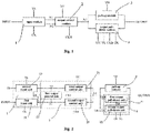
- the present embodiment provides a shift register unit, as shown in Fig.1 , comprising an input module 1, an output control module 2, a pull-up module 3 and an output pull-down module 4;
- the input module 1 is connected with a signal input terminal INPUT, a first clock signal input terminal CK and a low level signal terminal VL for providing a signal inputted at the signal input terminal INPUT to a first node N1 under the control of a signal inputted at the first clock signal input terminal CK, and controlling potential of a second node N2 under the control of the signal inputted at the first clock signal input terminal CK and a signal inputted at the low level signal terminal VL;
- the output control module 2 is connected with a second clock signal input terminal CKB and a high level signal terminal VH for controlling potential of a third node N3 under the control of the first node N1, the second node N2, a signal inputted at the second clock signal input terminal CKB and a high level signal inputted at the high level signal terminal VH;
- the output pull-down module 4 cooperates with the input module 1, the pull-up module 3 and the output control module 2 so that the signal output terminal OUTPUT of the shift register unit outputs a stable low level signal, resulting in an improved display quality; particularly, operation of the output pull-down module 4 in the present embodiment will not be affected by clock signals, which also ensures that the signal output terminal OUTPUT outputs the stable low level signal (details thereof will be described in conjunction with the method for driving the shift register as below).
- the input module 1 comprises a first input unit 11 and a second input unit 12, wherein: the first input unit 11 is connected with the signal input terminal INPUT and the first clock signal input terminal CK for controlling potential of the first node N1 under the control of the signal inputted at the first clock signal input terminal CK; the second input unit 12 is connected with the first node N1, the first clock signal input terminal CK and the low level signal terminal VL for controlling potential of the second node N2 under the control of the first node N1 and the signal inputted at the first clock signal input terminal CK.
- the output control module 2 comprises a first output control unit 21, a second output control unit 22 and a third output control unit 23, wherein the first output control unit 21 is connected between the first node N1 and the second node N2, and is connected with the second clock signal input terminal CKB and the high level signal terminal VH for pulling up potential of the first node N1 under the control of the second node N2 and the clock signal inputted at the second clock signal input terminal CKB; the second output control unit 22 is connected with the first node N1, the second clock signal input terminal CKB and the third node N3 for controlling potential of the third node N3 under the control of the potential of the first node N1 and the signal inputted at the second clock signal input terminal CKB; the third output control unit 23 is connected with the second node N2, the high level signal terminal VH and the third node N3 for outputting the high level signal inputted at the high level signal terminal VH to the third node N3 under the control of potential of the second node N2.
- the output pull-down module 4 comprises a first output pull-down unit 41 and a second output pull-down unit 42, the first output pull-down unit 41 and the second output pull-down unit 42 are connected with each other through a fourth node N4, the first output pull-down unit 41 is connected with the second clock signal input terminal CKB for pulling down potential of the signal output terminal OUTPUT under the control of the signal inputted at the second clock signal input terminal CKB; the second output pull-down unit 42 is connected with the high level signal terminal VH, the third node N3, the first clock signal input terminal CK and the low level signal terminal VL for pulling down potential of the signal output terminal OUTPUT to be potential of the low level signal terminal VL under the control of the potential of the third node N3 and the signal inputted at the first clock signal input terminal CK.
- the shift register unit of the present embodiment has a simple structure which is easy to be realized.
- the present embodiment provides a method for driving the above shift register unit, as shown in Fig.4 , comprising: in a first period t1, a low level signal is inputted at the signal input terminal INPUT, a low level signal is inputted at the first clock signal input terminal CK, a high level signal is inputted at the second clock signal input terminal CKB, the input module 1 pulls down potentials of the first node N1 and the second node N2 to be a low level, the output control module 2 controls so as to pull up potential of the third node N3 to be a high level, the output pull-down module 4 pulls down potential of the fourth node N4 to be a low level, and the signal output terminal OUTPUT outputs a low level signal.
- a high level signal is inputted at the signal input terminal INPUT, a high level signal is inputted at the first clock signal input terminal CK, a low level signal is inputted at the second clock signal input terminal CKB, the potential of the first node N1 is maintained to be the low level under the control of the output control module 2, the input terminal 1 pulls up the potential of the second node N2 to be a high level, the potential of the third node N3 is pulled down to be a low level, the pull-up module 3 outputs a high level signal to the signal output terminal OUTPUT, and the output pull-down module 4 maintains the potential of the signal output terminal OUTPUT to be a high level.
- a high level signal is inputted at the signal input terminal INPUT, a low level signal is inputted at the first clock signal input terminal CK, a high level signal is inputted at the second clock signal input terminal CKB, the input module 1 pulls up the potential of the first node N1 to be a high level, pulls down the potential of the second node N2 to be a low level, and the potential of the third node N3 is pulled up to be a high level under the control of the output control module 2, the potential of the fourth node N4 becomes a high level under the control of the output pull-down module 4, since the fourth node N4 discharges, and the signal output terminal OUTPUT outputs a potential lower than that in the second period t2.
- a high level signal is inputted at the signal input terminal INPUT
- a high level signal is inputted at the first clock signal input terminal CK
- a low level signal is inputted at the second clock signal input terminal CKB
- the output control module 2 maintains the potential of the first node N1 to be the high level and the potential of the second node N2 to be the low level
- the third node N3 outputs a high level under the control of the potential of the second node N2
- the output pull-down module 4 pulls down the potential of the fourth node N4 to be a low level
- the signal output terminal OUTPUT outputs a low level signal.
- a high level signal is inputted at the signal input terminal INPUT
- a low level signal is inputted at the first clock signal input terminal CK
- a high level signal is inputted at the second clock signal input terminal CKB
- the input module 1 maintains the potential of the first node N1 to be the high level
- the potential of the third node N3 is maintained to be the high level under the control of the potential of the second node N2
- the output pull-down module 4 maintains the potential of the fourth node N4 to be the low level
- the signal output terminal OUTPUT outputs a low level signal.
- the output pull-down module 4 cooperates with the input module 1, the pull-up module 3 and the output control module 2 so that the signal output terminal OUTPUT of the shift register unit outputs a stable low level signal, resulting in an improved display quality; particularly, the operation of the output pull-down module 4 in the present embodiment will not be affected by clock signals, which also ensures that the signal output terminal OUTPUT outputs the stable low level signal.
- the method for driving the shift register unit specifically comprises: in the first period t1, the low level signal is inputted at the signal input terminal INPUT, the low level signal is inputted at the first clock signal input terminal CK and the high level signal is inputted at the second clock signal input terminal CKB, the first input unit 11 pulls down the potential of the first node N1 to be the low level, the second input unit 12 pulls down the potential of the second node N2 to be the low level, the second and third output control units pull up the potential of the third node N3 to be the high level, the second output pull-down unit pulls down the potential of the fourth node N4 to be the low level, and the signal output terminal
- the high level signal is inputted at the signal input terminal INPUT
- the high level signal is inputted at the first clock signal input terminal CK
- the low level signal is inputted at the second clock signal input terminal CKB
- the potential of the first node N1 is maintained to be the low level under the control of the second output control unit 22
- the second input unit 12 pulls up the potential of the second node N2 to be the high level
- the second output control unit 22 pulls down the potential of the third node N3 to be the low level
- the pull-up module 3 outputs the high level signal to the signal output terminal OUTPUT
- the first output pull-down unit 41 maintains the potential of the signal output terminal OUTPUT to be the high level.
- the high level signal is inputted at the signal input terminal INPUT
- the low level signal is inputted at the first clock signal input terminal CK
- the high level signal is inputted at the second clock signal input terminal CKB
- the first input unit 11 pulls up the potential of the first node N1 to be the high level
- the second input unit 12 pulls down the potential of the second node N2 to be the low level
- the potential of the third node N3 is maintained to be the high level under the control of the third output control unit 23
- the potential of the fourth node N4 is pulled up to be the high level under the control of the first output pull-down unit 41
- the signal output terminal OUTPUT outputs the potential lower than that in the second period t2.
- the high level signal is inputted at the signal input terminal INPUT, the high level signal is inputted at the first clock signal input terminal CK, the low level signal is inputted at the second clock signal input terminal CKB, the third output control unit maintains the potential of the second node N2 to be the low level, the potential of the first node N1 is pulled up to be the high level by the first output control unit 21, the third node N3 is maintained to be the high level under the control of potential of the second node N2, the first output pull-down unit 41 pulls down the potential of the fourth node N4 to be the low level, and the signal output terminal OUTPUT outputs the low level signal.
- the high level signal is inputted at the signal input terminal INPUT
- the low level signal is inputted at the first clock signal input terminal CK
- the high level signal is inputted at the second clock signal input terminal CKB
- the first input unit 11 maintains the potential of the first node N1 to be the high level
- the second input unit 12 maintains the potential of the second node N2 to be the low level
- the third node N3 is maintained to be the high level under the control of the potential of the second node N2
- the second output pull-down unit 42 maintains the potential of the fourth node N4 to be the low level
- the signal output terminal OUTPUT outputs the low level signal.
- the method for driving the shift register unit has a simple timing sequence and is easy to be controlled, thus is easy to be achieved.
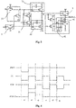
- the first input unit 11 comprises a first transistor T1
- the second input unit 12 comprises a second transistor T2 and a third transistor T3, wherein: a first electrode of the first transistor T1 is connected with the signal input terminal INPUT, a second electrode of the first transistor T1 is connected with a control electrode of the second transistor T2 and the first node N1, and a control electrode of the first transistor T1 is connected with the first clock signal input terminal CK; a first electrode of the second transistor T2 is connected with the first clock signal input terminal CK, and a second electrode of the second transistor T2 is connected with a second electrode of the third transistor T3 and the second node N2; a first electrode of the third transistor T3 is connected with the low level signal terminal VL, and a control electrode of the third transistor T3 is connected with the first clock signal input terminal CK.
- the first output control unit 21 comprises a sixth transistor T6 and a seventh transistor T7
- the second output control unit 22 comprises a fifth transistor T5 and a first capacitor C1
- the third output control unit 23 comprises a fourth transistor T4 and a second capacitor C2
- a first electrode of the sixth transistor T6 is connected with the high level signal terminal VH
- a second electrode of the sixth transistor T6 is connected with a first electrode of the seventh transistor T7
- a control electrode of the sixth transistor T6 is connected with the second electrode of the third transistor T3 and the second node N2
- a second electrode of the seventh transistor T7 is connected with the second electrode of the first transistor T1 and the first node N1
- a control electrode of the seventh transistor T7 is connected with the second clock signal input terminal CKB
- a first electrode of the fifth transistor T5 is connected with the second clock signal input terminal CKB
- a second electrode of the fifth transistor T5 is connected with the third node N3, and a control electrode of the fifth transistor T5 is connected with
- the first output pull-down unit 41 comprises a third capacitor C3 and a fourth capacitor C4, and the second output pull-down unit 42 comprises an eighth transistor T8, a ninth transistor T9 and an eleventh transistor T11, wherein: a first electrode of the eighth transistor T8 is connected with the high level signal terminal VH, a second electrode of the eighth transistor T8 is connected with a first electrode of the ninth transistor T9 and the fourth node N4, and a control electrode of the eighth transistor T8 is connected with the third node N3; a second electrode of the ninth transistor T9 is connected with the low level signal terminal VL, and a control electrode of the ninth transistor T9 is connected with the first clock signal input terminal CK; a first electrode of the eleventh transistor T11 is connected with the signal output terminal OUTPUT, a second electrode of the eleventh transistor T11 is connected with the low level signal terminal VL, and a control electrode of eleventh transistor T11 is connected with the fourth node N4; a first terminal of the third capacitor C3 is connected with the second clock signal input
- the pull-up module 3 comprises a tenth transistor T10, wherein a first electrode of the tenth transistor T10 is connected with the high level signal terminal VH, a second electrode of the tenth transistor T10 is connected with the signal output terminal OUTPUT, and a control electrode of the tenth transistor T10 is connected with the third node N3.
- the low level signal is inputted at the signal input terminal INPUT, the low level signal is inputted at the first clock signal input terminal CK, the high level signal is inputted at the second clock signal input terminal CKB, the first transistor T1 is turned on, since the low level signal is inputted at the signal input terminal INPUT, the potential of the first node N1 connecting the second electrode of the first transistor T1 and the control electrode of the fifth transistor T5 is the low level, so that the second transistor T2 and the fifth transistor T5 are turned on, at this time, at this time, since the high level signal is inputted at the second clock signal input terminal CKB, the potential of the third node N3 connecting the second electrode of the fourth transistor T4 and the second electrode of the fifth transistor T5 is the high level, further since the low level signal is inputted at the first clock signal input terminal CK, the third transistor T3 is also turned on, the potential of the second node N2 connecting the second electrode of the third transistor T3, the control electrode of the fourth transistor T4 and the first terminal
- the high level signal is inputted at the signal input terminal INPUT, the low level signal is inputted at the second clock signal input terminal CKB, the high level signal is inputted at the first clock signal input terminal CK, at this time, the first transistor T1 and the third transistor T3 are turned off, due to the maintaining function of the first capacitor C1, at this time, the first node N1 is still at a low level, since the low level signal is inputted at the second clock signal input terminal CKB, due to the coupling function of the first capacitor C1, the potential of the first node N1 is lower at this time, thus the potential of the third node N3 is pulled down, and the second transistor T2 is turned on, since the high level signal is inputted at the first clock signal input terminal CK, the potential of the second node N2 is pulled up, so that the fourth transistor T4 is turned off, the third node N3 is maintained to be the low level inputted at the second clock signal input terminal CKB, the eighth transistor T8 and the tenth transistor T10 are
- the high level signal is inputted at the signal input terminal INPUT
- the high level signal is inputted at the second clock signal input terminal CKB and the low level signal is inputted at the first clock signal input terminal CK
- the first transistor T1 is turned on, since the high level signal is inputted at the signal input terminal INPUT, the first node N1 is at a high level, so that the second transistor T2 and the fifth transistor T5 are turned off, since the low level signal is inputted at the first clock signal input terminal CK, the third transistor T3 is thus turned on, the second node N2 is at a low level, thereby the fourth transistor T4 is turned on, and the third node N3 is at a high level, since the third node N3 is at a high level, the eighth transistor T8 and the tenth transistor T10 are turned off, due to the coupling effect of the third capacitor C3 and the maintaining function of the fourth capacitor C4, the potential of the fourth node N4 becomes high level instantaneously and then is maintained to be the
- the high level signal is inputted at the signal input terminal INPUT, the low level signal is inputted at the second clock signal input terminal CKB and the high level signal is inputted at the first clock signal input terminal CK, at this time, the first transistor T1 and the third transistor T3 are turned off, the first node N1 is at a high level, and the second transistor T2 and the fifth transistor T5 are turned off; due to the maintaining function of the second capacitor C2, the second node N2 is at a low level, the sixth transistor T6 is turned on, and since the low level signal is inputted at the second clock signal input terminal CKB, the seventh transistor T7 is turned on, thereby the first node N1 is maintained at a high level, the third node N3 is not affected by the signal inputted at the second clock signal input terminal CKB and is maintained to be the high level, meanwhile since the second node N2 is at a low level, the fourth transistor T4 is turned on, the third node N3 is still at a high level, the eighth
- the high level signal is inputted at the signal input terminal INPUT
- the high level signal is inputted at the second clock signal input terminal CKB and the low level signal is inputted at the first clock signal input terminal CK
- the first transistor T1 is turned on
- the third transistor T3 is turned on
- the second node N 2 is at a low level
- the fourth transistor T4 is turned on
- the third node N3 is at a high level
- the eighth transistor T8 and the tenth transistor T10 are turned off, since the low level of the third node N3 at the last moment is maintained by the fourth capacitor C4, at this time, due to the coupling effect of the third capacitor C3, the potential of the fourth node N4 is pulled up instantaneously, but since the ninth transistor T9 is turned on, the fourth node N4 is reset to be
- the shift register unit preferably comprises a fourth capacitor C4, of course, the fourth capacitor C4 may be not contained, which will not affect the whole operation state, details are omitted here.
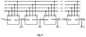
- the present embodiment provides a shift register comprising a plurality of the above shift register units cascaded together, wherein the signal outputted from the signal output terminal OUTPUT of each shift register unit is used as the signal inputted into the signal input terminal INPUT of the next stage, the signal input terminal INPUT of the shift register unit of the first stage is connected with a frame strobe signal STV.
- the first clock signal input terminal CK, the second clock signal input terminal CKB, the high level signal terminal VH, the low level signal terminal VL in each shift register unit are respectively connected with the signal lines corresponding thereto for introducing the corresponding signals respectively.
- Signals inputted the signal input terminals INPUTs of the shift register units are Ei ⁇ 1>,Ei ⁇ 2>;Ei ⁇ N+1> respectively, wherein Ei ⁇ 1> is a STV signal, each signal output terminal OUTPUT is also used as input of the shift register unit of the next stage, for example, the signal outputted from the signal output terminal OUTPUT of the first shift register unit is the signal Ei ⁇ 2> inputted into the signal input terminal INPUT of the second shift register unit.
- the signal output terminals OUTPUTs are respectively connected with the pixel units (i.e., Eo ⁇ 1>,Eo ⁇ 2>. «Eo ⁇ N>) corresponding thereto, so that the light emitting devices in the pixel units emit light.
- the present embodiment also provides a display apparatus comprising the above shift register.
- the display apparatus may be a phone, a tablet computer, a television, a monitor, a notebook computer, a digital photo frame, a navigator or any other product or component with display function.
- the display apparatus of the present embodiment comprises the above shift register, it has better performance.
- the display apparatus of the present embodiment may further comprise other conventional configurations such as a display driving unit and so on.
Landscapes
- Engineering & Computer Science (AREA)
- Microelectronics & Electronic Packaging (AREA)
- Physics & Mathematics (AREA)
- Computer Hardware Design (AREA)
- General Physics & Mathematics (AREA)
- Theoretical Computer Science (AREA)
- Power Engineering (AREA)
- Control Of Indicators Other Than Cathode Ray Tubes (AREA)
- Shift Register Type Memory (AREA)
Claims (6)
- Unité de registre à décalage, comprenant un module d'entrée (1), un module de rappel vers le niveau haut (3), un module de contrôle de sortie (2) et un module de rappel vers le niveau bas de sortie (4), dans lequel :le module d'entrée (1) est connecté à une borne d'entrée de signal (INPUT), une première borne d'entrée de signal d'horloge (CK) et une borne de signal de bas niveau (VL), et est configuré pour fournir un signal entré au niveau de la borne d'entrée de signal (INPUT) à un premier nœud (N1) sous le contrôle d'un signal entré au niveau de la première borne d'entrée de signal d'horloge (CK), et un potentiel de contrôle d'un second nœud (N2) sous le contrôle du signal entré au niveau de la première borne d'entrée de signal d'horloge (CK) et un signal de bas niveau entré au niveau de la borne de signal de bas niveau (VL) ;le module de contrôle de sortie (2) est connecté à une deuxième borne d'entrée de signal d'horloge (CKB) et à une borne de signal de haut niveau (VH), et est configuré pour contrôler le potentiel d'un troisième nœud (N3) sous le contrôle d'un potentiel du premier nœud (N1), le potentiel du deuxième nœud (N2), un signal entré au niveau de la deuxième borne d'entrée de signal d'horloge (CKB) et un signal de haut niveau entré au niveau de la borne de signal de haut niveau (VH) ;le module de rappel vers le niveau haut (3) est connecté à la borne de signal de haut niveau (VH), et est configuré pour remonter le niveau d'une borne de sortie de signal (OUTPUT) à un haut niveau sous le contrôle du potentiel du troisième nœud (N3) ; etle module de rappel vers le niveau bas de sortie (4) est connecté à la première borne d'entrée de signal d'horloge (CK), à la seconde borne d'entrée de signal d'horloge (CKB), à la borne de signal de haut niveau (VH) et à la borne de signal de bas niveau (VL), et est configuré pour abaisser le potentiel de la borne de sortie de signal (OUTPUT) sous le contrôle du potentiel du troisième nœud (N3), le signal entré au niveau de la première borne d'entrée de signal d'horloge (CK), le signal entré au niveau de la deuxième borne d'entrée de signal d'horloge (CKB), le signal de haut niveau entré au niveau de la borne de signal de haut niveau (VH) et le signal de bas niveau entré au niveau de la borne de signal de bas niveau (VL),dans lequel le module de rappel vers le niveau bas de sortie (4) comprend une première unité de rappel vers le niveau bas de sortie (41) et une deuxième unité de rappel vers le niveau bas de sortie (42), la première unité de rappel vers le niveau bas de sortie (41) et la deuxième unité de rappel vers le niveau bas de sortie (42) sont connectées les unes aux autres via le quatrième nœud (N4) ;la première unité de rappel vers le niveau bas de sortie (41) est connectée à la deuxième borne d'entrée de signal d'horloge (CKB), et est configurée pour abaisser le potentiel de la borne de sortie de signal (OUTPUT) sous le contrôle du signal entré au niveau de la deuxième borne d'entrée de signal d'horloge (CKB) ;la deuxième unité de rappel vers le niveau bas de sortie (42) est connectée à la borne de signal de haut niveau (VH), au troisième nœud (N3), à la première borne d'entrée de signal d'horloge (CK) et à la borne de signal de bas niveau (VL), et est configurée pour abaisser le potentiel de la borne de sortie de signal (OUTPUT) pour être le potentiel de la borne de signal de bas niveau (VL) sous le contrôle du potentiel du troisième nœud (N3) et du signal entré au niveau de la première entrée de signal d'horloge terminal (CK) ; etdans lequel la première unité de rappel vers le niveau bas de sortie (41) comprend un troisième condensateur (C3), et la deuxième unité de rappel vers le niveau bas de sortie (42) comprend un huitième transistor (T8), un neuvième transistor (T9) et un onzième transistor (T11), dans lequel :une première électrode du huitième transistor (T8) est connectée à la borne de signal de haut niveau (VH), une deuxième électrode du huitième transistor (T8) est connectée à une première électrode du neuvième transistor (T9) et au quatrième nœud (N4), et une électrode de contrôle du huitième transistor (T8) est connectée au troisième nœud (N3) ;une seconde électrode du neuvième transistor (T9) est connectée à la borne de signal de bas niveau (VL), et une électrode de contrôle du neuvième transistor (T9) est connectée à la première borne d'entrée de signal d'horloge (CK) ;une première électrode du onzième transistor (T11) est connectée à la borne de sortie de signal (OUTPUT), une deuxième électrode du onzième transistor (T11) est connectée à la borne de signal de bas niveau (VL), et une électrode de contrôle du onzième le transistor (T11) est connectée au quatrième nœud (N4) ;une première borne du troisième condensateur (C3) est connectée à la deuxième borne d'entrée de signal d'horloge (CKB), et une deuxième borne du troisième condensateur (C3) est connectée au quatrième nœud (N4),dans lequel le module d'entrée (1) comprend une première unité d'entrée et une deuxième unité d'entrée,la première unité d'entrée est connectée à la borne d'entrée de signal (INPUT) et à la première borne d'entrée de signal d'horloge (CK), et est configurée pour contrôler le potentiel du premier nœud (N1) sous le contrôle du signal entré au niveau de la première borne d'entrée de signal d'horloge (CK) ;la deuxième unité d'entrée est connectée au premier nœud (N1), à la première borne d'entrée de signal d'horloge (CK) et à la borne de signal de bas niveau (VL), et est configurée pour contrôler le potentiel du deuxième nœud (N2) sous le contrôle du potentiel du premier nœud (N1) et du signal entré au niveau de la première borne d'entrée de signal d'horloge (CK),dans lequel la première unité d'entrée comprend un premier transistor (T1), et la deuxième unité d'entrée comprend un deuxième transistor (T2) et un troisième transistor (T3),une première électrode du premier transistor (T1) est connectée à la borne d'entrée de signal (INPUT), une deuxième électrode du premier transistor (T1) est connectée à une électrode de contrôle du deuxième transistor (T2) et au premier nœud (N1), et une électrode de contrôle du premier transistor (T1) est connectée à la première borne d'entrée de signal d'horloge (CK) ;la première électrode du deuxième transistor (T2) est connectée à la première borne d'entrée de signal d'horloge (CK), et une seconde électrode du deuxième transistor (T2) est connectée à une deuxième électrode du troisième transistor (T3) et au deuxième nœud (N2) ;une première électrode du troisième transistor (T3) est connectée à la borne de signal de bas niveau (VL), et une électrode de contrôle du troisième transistor (T3) est connectée à la première borne d'entrée de signal d'horloge (CK),dans lequel le module de contrôle de sortie (2) comprend une première unité de contrôle de sortie (21), une deuxième unité de contrôle de sortie (22) et une troisième unité de contrôle de sortie (23),la première unité de contrôle de sortie (21) est connectée entre le premier nœud (N1) et le deuxième nœud (N2), et est connecté à la deuxième borne d'entrée de signal d'horloge (CKB) et à la borne de signal de haut niveau (VH), et est configurée pour augmenter le potentiel du premier nœud (N1) sous le contrôle du potentiel du deuxième nœud (N2) et du signal entré au niveau de la deuxième borne d'entrée de signal d'horloge (CKB) ;la deuxième unité de contrôle de sortie (22) est connectée au premier nœud (N1), à la deuxième borne d'entrée de signal d'horloge (CKB) et au troisième nœud (N3), et est configurée pour contrôler le potentiel du troisième nœud (N3) sous le contrôle du potentiel du premier nœud (N1) et du signal entré au niveau de la deuxième borne d'entrée de signal d'horloge (CKB) ;la troisième unité de contrôle de sortie (23) est connectée au deuxième nœud (N2), à la borne de signal de haut niveau (VH) et au troisième nœud (N3), et est configurée pour délivrer le signal de haut niveau entré au niveau de la borne de signal de haut niveau (VH) au niveau du troisième nœud (N3) sous le contrôle du potentiel du deuxième nœud (N2),dans lequel la première unité de contrôle de sortie (21) comprend un sixième transistor (T6) et un septième transistor (T7), la deuxième unité de contrôle de sortie (22) comprend un cinquième transistor (T5) et un premier condensateur (C1), et la troisième unité de contrôle de sortie (23) comprend un quatrième transistor (T4) et un deuxième condensateur (C2) ;une première électrode du sixième transistor (T6) est connectée à la borne de signal de haut niveau (VH), une deuxième électrode du sixième transistor (T6) est connectée à une première électrode du septième transistor (T7), et une électrode de contrôle du sixième transistor (T6) est connectée à la deuxième électrode du troisième transistor (T3) et au deuxième nœud (N2) ;une seconde électrode du septième transistor (T7) est connectée à la deuxième électrode du premier transistor (T1) et au premier nœud (N1), et une électrode de contrôle du septième transistor (T7) est connectée à la seconde borne d'entrée de signal d'horloge (CKB) ;une première électrode du cinquième transistor (T5) est connectée à la deuxième borne d'entrée de signal d'horloge (CKB), une deuxième électrode du cinquième transistor (T5) est connectée au troisième nœud (N3), et une électrode de contrôle du cinquième le transistor (T5) est connectée à la deuxième électrode du premier transistor (T1) ;une première borne du premier condensateur (C1) est connectée à la deuxième électrode du premier transistor (T1) et à la deuxième électrode du septième transistor (T7), et une deuxième borne du premier condensateur (C1) est connectée à un troisième nœud (N3) et à la deuxième électrode du cinquième transistor (T5) ;une première électrode du quatrième transistor (T4) est connectée à la borne de signal de haut niveau (VH), une deuxième électrode du quatrième transistor (T4) est connectée à la deuxième électrode du cinquième transistor (T5), et une électrode de contrôle du quatrième transistor (T4) est connectée à la deuxième électrode du troisième transistor (T3) ;une première borne du deuxième condensateur (C2) est connectée à la deuxième électrode du deuxième transistor (T2) et au deuxième nœud (N2), et une deuxième borne du deuxième condensateur (C2) est connectée à la première électrode du quatrième transistor (T4) et à la borne de signal de haut niveau (VH),dans lequel le module de rappel vers le niveau haut (3) comprend un dixième transistor (T10),une première électrode du dixième transistor (T10) est connectée à la borne de signal de haut niveau (VH), une deuxième électrode du dixième transistor (T10) est connectée à la borne de sortie de signal (OUTPUT), et une électrode de contrôle du dixième transistor (T10) est connectée au troisième nœud (N3).
- Unité de registre à décalage selon la revendication 1, dans laquelle la première unité de rappel vers le niveau bas de sortie (41) comprend en outre un quatrième condensateur (C4) ; et
une première borne du quatrième condensateur (C4) est connectée au quatrième nœud (N4), et une deuxième borne du quatrième condensateur (C4) est connectée à la borne de sortie de signal (OUTPUT). - Registre à décalage, comprenant une pluralité d'unités de registre à décalage en cascade, dont chacune est l'unité de registre à décalage selon l'une quelconque des revendications 1 à 2.
- Appareil d'affichage, comprenant le registre à décalage selon la revendication 3.
- Procédé de pilotage de l'unité de registre à décalage selon la revendication 1, comprenant les étapes consistant à :dans une première période, entrer un signal de bas niveau au niveau de la borne d'entrée de signal (INPUT), entrer un signal de bas niveau au niveau de la première borne d'entrée de signal d'horloge (CK) et entrer un signal de haut niveau au niveau de la deuxième borne d'entrée de signal d'horloge (CKB), abaisser les potentiels du premier nœud (N1) et du deuxième nœud (N2) pour qu'ils soient à un bas niveau par le module d'entrée (1), relever le potentiel du troisième nœud (N3) à un haut niveau par le module de contrôle de sortie (2), abaisser le potentiel du quatrième nœud (N4) à un bas niveau par le module de rappel vers le niveau bas de sortie (4), et délivrer un signal de bas niveau au niveau de la borne de sortie de signal (OUTPUT) ;dans une deuxième période, entrer un signal de haut niveau au niveau de la borne d'entrée de signal (INPUT), entrer un signal de haut niveau au niveau de la première borne d'entrée de signal d'horloge (CK) et entrer un signal de bas niveau au niveau de la deuxième borne d'entrée de signal d'horloge (CKB), maintenir le potentiel du premier nœud (N1) à un bas niveau sous le contrôle du module de contrôle de sortie (2),abaisser le potentiel du troisième nœud (N3) à un bas niveau, relever le potentiel du deuxième nœud (N2) à un haut niveau par le module d'entrée (1), délivrer un signal de haut niveau au niveau de la borne de sortie de signal (OUTPUT) par le module de rappel vers le niveau haut (3), maintenir le potentiel de la borne de sortie de signal (OUTPUT) à un haut niveau par le module de rappel vers le niveau bas de sortie (4) ;dans une troisième période, entrer un signal de haut niveau au niveau de la borne d'entrée de signal (INPUT), entrer un signal de bas niveau au niveau de la première borne d'entrée de signal d'horloge (CK) et entrer un signal de haut niveau au niveau de la deuxième borne d'entrée de signal d'horloge (CKB), relever le potentiel du premier nœud (N1) à un haut niveau et abaisser le potentiel du deuxième nœud (N2) à un bas niveau par le module d'entrée (1), et relever le potentiel du troisième nœud (N3) à un haut niveau sous le contrôle du module de contrôle de sortie (2), et amener le potentiel du quatrième nœud (N4) à un haut niveau sous le contrôle du module de rappel vers le niveau haut de sortie (4), de sorte qu'un potentiel au niveau de la borne de sortie de signal (OUTPUT) est inférieur à celui de la deuxième période depuis la décharge du quatrième nœud (N4) ;dans une quatrième période, entrer un signal de haut niveau au niveau de la borne d'entrée de signal (INPUT), entrer un signal de haut niveau au niveau de la première borne d'entrée de signal d'horloge (CK) et entrer un signal de bas niveau au niveau de la deuxième borne d'entrée de signal d'horloge (CKB), maintenir le potentiel du premier nœud (N1) à un haut niveau et le potentiel du deuxième nœud (N2) à un bas niveau par le module de contrôle de sortie (2), délivrer un signal de haut niveau au niveau du troisième nœud (N3) sous le contrôle du potentiel du deuxième nœud (N2), abaisser le potentiel du quatrième nœud (N4) à un bas niveau par le module de rappel vers le niveau bas de sortie (4), et délivrer un signal de bas niveau au niveau de la borne de sortie de signal (OUTPUT) ;dans une cinquième période, entrer un signal de haut niveau au niveau de la borne d'entrée de signal (INPUT), entrer un signal de bas niveau au niveau de la première borne d'entrée de signal d'horloge (CK) et entrer un signal de haut niveau au niveau de la deuxième borne d'entrée de signal d'horloge (CKB), maintenir le potentiel du premier nœud (N1) à un haut niveau et le potentiel du deuxième nœud (N2) à un bas niveau par le module d'entrée (1), délivrer un signal de haut niveau au niveau du troisième nœud (N3) sous le contrôle du potentiel du deuxième nœud (N2), abaisser le potentiel du quatrième nœud (N4) à un bas niveau par le module de rappel vers le niveau bas de sortie (4), et délivrer un signal de bas niveau au niveau de la borne de sortie de signal (OUTPUT).
- Procédé selon la revendication 5, dans lequel le module d'entrée (1) comprend une première unité d'entrée et une deuxième unité d'entrée ; le module de contrôle de sortie (2) comprend une première unité de contrôle de sortie (21), une deuxième unité de contrôle de sortie (22) et une troisième unité de contrôle de sortie (23) ; le module de sortie vers le bas (4) comprend une première unité de rappel vers le niveau bas de sortie (41) et une deuxième unité de rappel vers le niveau bas de sortie (42) ; le procédé comprend :dans la première période, les étapes consistant à entrer le signal de bas niveau au niveau de la borne d'entrée de signal (INPUT), entrer le signal de bas niveau au niveau de la première borne d'entrée de signal d'horloge (CK) et entrer le signal de haut niveau au niveau de la deuxième borne d'entrée de signal d'horloge (CKB), abaisser le potentiel du premier nœud (N1) à un bas niveau par la première unité d'entrée, abaisser le potentiel du deuxième nœud (N2) à un bas niveau par la deuxième unité d'entrée, relever le potentiel du troisième nœud (N3) à un haut niveau par les deuxième et troisième unités de contrôle de sortie (22, 23), abaisser le potentiel du quatrième nœud (N4) à un bas niveau par la deuxième unité de rappel vers le niveau bas de sortie (42), et délivrer le signal de bas niveau au niveau de la borne de sortie de signal (OUTPUT) ;dans la deuxième période, les étapes consistant à entrer le signal de haut niveau au niveau de la borne d'entrée de signal (INPUT), entrer le signal de haut niveau au niveau de la première borne d'entrée de signal d'horloge (CK) et entrer le signal de bas niveau au niveau de la deuxième borne d'entrée de signal d'horloge (CKB), maintenir le potentiel du premier nœud (N1) à un bas niveau sous le contrôle de la deuxième unité de contrôle de sortie (22), relever le potentiel du deuxième nœud (N2) à un haut niveau par la seconde unité d'entrée, abaisser le potentiel du troisième nœud (N3) à un bas niveau par la deuxième unité de contrôle de sortie (22), délivrer le signal de haut niveau au niveau de la borne de sortie de signal (OUTPUT) par le module de rappel vers le niveau haut (3), maintenir le potentiel de la borne de sortie de signal (OUTPUT) à un haut niveau par la première unité de rappel vers le niveau bas de sortie (41) ;dans la troisième période, entrer le signal de haut niveau au niveau de la borne d'entrée de signal (INPUT), entrer le signal de bas niveau au niveau de la première borne d'entrée de signal d'horloge (CK) et entrer le signal de haut niveau au niveau de la deuxième borne d'entrée de signal d'horloge (CKB), relever le potentiel du premier nœud (N1) à un haut niveau par la première unité d'entrée, abaisser le potentiel du deuxième nœud (N2) à un bas niveau par la deuxième unité d'entrée, relever le potentiel du troisième nœud (N3) à un haut niveau sous le contrôle de la troisième unité de contrôle de sortie (23), relever le potentiel du quatrième nœud (N4) à un haut niveau sous le contrôle de la première unité de rappel vers le niveau bas de sortie (41), de sorte que le potentiel au niveau de la borne de sortie de signal (OUTPUT) est inférieur à celui de la deuxième période depuis la décharge du quatrième nœud (N4) ;dans la quatrième période, entrer le signal de haut niveau au niveau de la borne d'entrée de signal (INPUT), entrer le signal de haut niveau au niveau de la première borne d'entrée de signal d'horloge (CK) et entrer le signal de bas niveau au niveau de la deuxième borne d'entrée de signal d'horloge (CKB), maintenir le potentiel du deuxième nœud (N2) à un bas niveau par la troisième unité de contrôle de sortie (23), relever le potentiel du premier nœud (N1) à un haut niveau par la première unité de contrôle de sortie (21), délivrer le signal de haut niveau au niveau du troisième nœud (N3) sous le contrôle du potentiel du deuxième nœud (N2), abaisser le potentiel de le quatrième nœud (N4) à un bas niveau par la première unité de rappel vers le niveau bas de sortie (41), et délivrer le signal de bas niveau au niveau de la borne de sortie de signal (OUTPUT) ;dans la cinquième période, entrer le signal de haut niveau au niveau de la borne d'entrée de signal (INPUT), entrer le signal de bas niveau au niveau de la première borne d'entrée de signal d'horloge (CK) et entrer le signal de haut niveau au niveau de la deuxième borne d'entrée de signal d'horloge (CKB), maintenir le potentiel du premier nœud (N1) à un haut niveau par la première unité d'entrée, maintenir le potentiel du deuxième nœud (N2) à un bas niveau par la deuxième unité d'entrée, délivrer le signal de haut niveau au niveau du troisième nœud (N3) sous le contrôle du potentiel du deuxième nœud (N2), maintenir le potentiel du quatrième nœud (N4) à un bas niveau par la deuxième unité de rappel vers le niveau bas de sortie (42), et délivrer le signal de bas niveau au niveau de la borne de sortie de signal (OUTPUT).
Applications Claiming Priority (2)
| Application Number | Priority Date | Filing Date | Title |
|---|---|---|---|
| CN201410669868.0A CN104318904B (zh) | 2014-11-20 | 2014-11-20 | 移位寄存器单元及其驱动方法、移位寄存器、显示装置 |
| PCT/CN2015/076635 WO2016078304A1 (fr) | 2014-11-20 | 2015-04-15 | Unité de registre de décalage et son procédé d'actionnement, registre de décalage et dispositif d'affichage |
Publications (3)
| Publication Number | Publication Date |
|---|---|
| EP3223268A1 EP3223268A1 (fr) | 2017-09-27 |
| EP3223268A4 EP3223268A4 (fr) | 2018-08-15 |
| EP3223268B1 true EP3223268B1 (fr) | 2020-05-06 |
Family
ID=52374128
Family Applications (1)
| Application Number | Title | Priority Date | Filing Date |
|---|---|---|---|
| EP15762909.8A Active EP3223268B1 (fr) | 2014-11-20 | 2015-04-15 | Unité de registre de décalage et son procédé d'actionnement, registre de décalage et dispositif d'affichage |
Country Status (4)
| Country | Link |
|---|---|
| US (1) | US9754531B2 (fr) |
| EP (1) | EP3223268B1 (fr) |
| CN (1) | CN104318904B (fr) |
| WO (1) | WO2016078304A1 (fr) |
Cited By (1)
| Publication number | Priority date | Publication date | Assignee | Title |
|---|---|---|---|---|
| US11875722B2 (en) | 2020-06-24 | 2024-01-16 | Boe Technology Group Co., Ltd. | Display panel and display device |
Families Citing this family (50)
| Publication number | Priority date | Publication date | Assignee | Title |
|---|---|---|---|---|
| CN104318904B (zh) * | 2014-11-20 | 2017-08-01 | 京东方科技集团股份有限公司 | 移位寄存器单元及其驱动方法、移位寄存器、显示装置 |
| US9905312B2 (en) * | 2014-12-03 | 2018-02-27 | Nlt Technologies, Ltd. | Shift register circuit, gate driver and display apparatus |
| CN104835531B (zh) * | 2015-05-21 | 2018-06-15 | 京东方科技集团股份有限公司 | 一种移位寄存器单元及其驱动方法、移位寄存器和显示装置 |
| CN104900189B (zh) * | 2015-06-19 | 2017-08-01 | 京东方科技集团股份有限公司 | 移位寄存器单元及其驱动方法、移位寄存器和显示装置 |
| CN104867438B (zh) * | 2015-06-24 | 2018-02-13 | 合肥鑫晟光电科技有限公司 | 移位寄存器单元及其驱动方法、移位寄存器和显示装置 |
| CN105304057B (zh) | 2015-12-09 | 2018-11-30 | 京东方科技集团股份有限公司 | 一种移位寄存器及其驱动方法、栅极驱动电路 |
| CN105609054B (zh) * | 2016-02-29 | 2018-05-08 | 信利(惠州)智能显示有限公司 | 一种发光控制电路及移位寄存器 |
| CN105761757B (zh) * | 2016-05-13 | 2018-05-18 | 京东方科技集团股份有限公司 | 移位寄存器单元、驱动方法、阵列基板、显示面板和装置 |
| CN105788508B (zh) * | 2016-05-24 | 2017-07-25 | 京东方科技集团股份有限公司 | 一种栅极驱动电路及显示面板 |
| CN106057143A (zh) * | 2016-05-30 | 2016-10-26 | 京东方科技集团股份有限公司 | 移位寄存器及其操作方法、栅极驱动电路和显示装置 |
| CN106782399A (zh) * | 2017-01-11 | 2017-05-31 | 京东方科技集团股份有限公司 | 一种移位寄存器、其驱动方法、栅极驱动电路及显示装置 |
| KR102735537B1 (ko) * | 2017-02-20 | 2024-12-02 | 삼성디스플레이 주식회사 | 스테이지 회로 및 이를 이용한 주사 구동부 |
| CN106952625B (zh) * | 2017-04-24 | 2019-06-07 | 京东方科技集团股份有限公司 | 移位寄存器、其驱动方法、栅极驱动电路及显示面板 |
| CN106910453A (zh) * | 2017-05-09 | 2017-06-30 | 京东方科技集团股份有限公司 | 移位寄存器、其驱动方法、栅极集成驱动电路及显示装置 |
| CN107039014B (zh) * | 2017-05-26 | 2019-03-05 | 京东方科技集团股份有限公司 | 移位寄存器单元、其驱动方法、栅极驱动电路及显示面板 |
| CN107093414B (zh) * | 2017-07-03 | 2019-04-30 | 京东方科技集团股份有限公司 | 一种移位寄存器、其驱动方法、栅极驱动电路及显示装置 |
| CN107452318B (zh) * | 2017-09-20 | 2020-04-28 | 京东方科技集团股份有限公司 | 复位控制模块、其驱动方法及移位寄存器单元、显示装置 |
| CN108039150B (zh) * | 2017-11-16 | 2020-05-19 | 武汉华星光电半导体显示技术有限公司 | 移位寄存电路及移位寄存单元 |
| CN108320692B (zh) * | 2018-02-14 | 2022-01-07 | 京东方科技集团股份有限公司 | 移位寄存器单元及驱动方法、栅极驱动电路、显示面板 |
| CN108172192B (zh) * | 2018-03-20 | 2020-11-03 | 京东方科技集团股份有限公司 | 移位寄存器单元、驱动方法、栅极驱动电路和显示设备 |
| CN108389545A (zh) * | 2018-03-23 | 2018-08-10 | 京东方科技集团股份有限公司 | 移位寄存器单元、驱动方法、栅极驱动电路及显示装置 |
| CN108257550A (zh) * | 2018-03-30 | 2018-07-06 | 京东方科技集团股份有限公司 | 像素电路及其驱动方法、阵列基板、显示面板 |
| CN108573734B (zh) * | 2018-04-28 | 2019-10-25 | 上海天马有机发光显示技术有限公司 | 一种移位寄存器及其驱动方法、扫描驱动电路和显示装置 |
| US10777149B2 (en) * | 2018-05-10 | 2020-09-15 | Wuhan China Star Optoelectronics Semiconductor Display Technology Co., Ltd. | Driving circuit |
| CN110660362B (zh) * | 2018-06-28 | 2021-01-22 | 京东方科技集团股份有限公司 | 移位寄存器及栅极驱动电路 |
| CN109935201B (zh) | 2018-08-29 | 2020-10-09 | 合肥鑫晟光电科技有限公司 | 移位寄存器单元、栅极驱动电路、显示装置及驱动方法 |
| US11640795B2 (en) | 2018-08-29 | 2023-05-02 | Boe Technology Group Co., Ltd. | Shift register unit, gate drive circuit and drive method |
| CN209265989U (zh) | 2018-12-06 | 2019-08-16 | 北京京东方技术开发有限公司 | 移位寄存器、发光控制电路、显示面板 |
| US11308854B2 (en) | 2019-03-22 | 2022-04-19 | Boe Technology Group Co., Ltd. | Shift register unit, driving circuit, display device and driving method |
| CN110033734B (zh) * | 2019-04-25 | 2021-08-10 | 京东方科技集团股份有限公司 | 一种显示驱动电路及其驱动方法、显示装置 |
| EP4036900A4 (fr) * | 2019-09-25 | 2022-09-07 | BOE Technology Group Co., Ltd. | Unité de registre à décalage, procédé d'attaque, circuit d'attaque de grille et dispositif d'affichage |
| US11538395B2 (en) * | 2020-03-18 | 2022-12-27 | Boe Technology Group Co., Ltd. | Shift register unit and driving method thereof, gate drive circuit, and display device |
| CN111415624B (zh) * | 2020-04-29 | 2021-05-14 | 京东方科技集团股份有限公司 | 移位寄存器电路及其驱动方法、栅极驱动电路、显示装置 |
| CN111768733B (zh) * | 2020-06-10 | 2022-08-30 | 京东方科技集团股份有限公司 | 发光控制信号生成电路、方法和显示装置 |
| WO2022082719A1 (fr) * | 2020-10-23 | 2022-04-28 | 京东方科技集团股份有限公司 | Unité de registre à décalage, procédé d'attaque, circuit d'attaque et appareil d'affichage |
| WO2022133800A1 (fr) * | 2020-12-23 | 2022-06-30 | 京东方科技集团股份有限公司 | Registre à décalage et procédé d'attaque associé, dispositif d'attaque de grille et appareil d'affichage |
| CN112802422B (zh) | 2021-01-29 | 2022-06-10 | 云谷(固安)科技有限公司 | 移位寄存器、栅极驱动电路和显示面板 |
| EP4120229A4 (fr) * | 2021-03-09 | 2023-06-28 | BOE Technology Group Co., Ltd. | Registre à décalage, circuit d'attaque et substrat d'affichage |
| CN115380323A (zh) * | 2021-03-19 | 2022-11-22 | 京东方科技集团股份有限公司 | 移位寄存器单元及驱动方法、栅极驱动电路、显示装置 |
| CN115398532B (zh) * | 2021-03-24 | 2023-11-28 | 京东方科技集团股份有限公司 | 显示基板及其制备方法、显示装置 |
| CN113436580B (zh) * | 2021-06-18 | 2022-06-10 | 武汉华星光电半导体显示技术有限公司 | 栅极驱动电路及显示面板 |
| CN113345365B (zh) * | 2021-06-25 | 2022-03-29 | 合肥维信诺科技有限公司 | 移位寄存器、显示驱动器及显示面板 |
| CN113539185B (zh) * | 2021-07-29 | 2022-12-23 | 合肥京东方卓印科技有限公司 | 显示装置、栅极驱动电路、移位寄存单元及其驱动方法 |
| WO2023060567A1 (fr) | 2021-10-15 | 2023-04-20 | 京东方科技集团股份有限公司 | Substrat d'affichage et appareil d'affichage |
| CN113889022A (zh) * | 2021-10-27 | 2022-01-04 | 合肥维信诺科技有限公司 | 移位寄存器、显示面板和显示装置 |
| US12125428B2 (en) | 2021-11-29 | 2024-10-22 | Boe Technology Group Co., Ltd. | Shift register and driving method thereof, light emission control driver and display apparatus |
| CN116648787A (zh) * | 2021-12-22 | 2023-08-25 | 京东方科技集团股份有限公司 | 显示基板及其制备方法、显示装置 |
| CN114333705A (zh) * | 2021-12-30 | 2022-04-12 | 厦门天马显示科技有限公司 | 驱动电路、显示面板、显示装置和稳压控制方法 |
| CN114974077A (zh) * | 2022-06-29 | 2022-08-30 | 武汉天马微电子有限公司 | 移位寄存器及其驱动方法、发光控制电路、显示面板 |
| CN116959359A (zh) * | 2023-08-07 | 2023-10-27 | 上海天马微电子有限公司 | 显示面板和显示装置 |
Family Cites Families (21)
| Publication number | Priority date | Publication date | Assignee | Title |
|---|---|---|---|---|
| KR100685307B1 (ko) | 1999-11-05 | 2007-02-22 | 엘지.필립스 엘시디 주식회사 | 쉬프트 레지스터 |
| KR20050114850A (ko) | 2004-06-02 | 2005-12-07 | 엘지.필립스 엘시디 주식회사 | 쉬프트 레지스터와 이를 이용한 액정표시장치 |
| US7310402B2 (en) * | 2005-10-18 | 2007-12-18 | Au Optronics Corporation | Gate line drivers for active matrix displays |
| CN101241247B (zh) * | 2007-02-09 | 2010-05-26 | 群康科技(深圳)有限公司 | 移位寄存器及液晶显示装置 |
| BRPI0920739A2 (pt) * | 2008-10-30 | 2015-12-29 | Sharp Kk | circuito de registro de deslocamento e dispositivo de exibição, e método para acionar circuito de registro |
| CN101783124B (zh) * | 2010-02-08 | 2013-05-08 | 北京大学深圳研究生院 | 栅极驱动电路单元、栅极驱动电路及显示装置 |
| CN102654982B (zh) * | 2011-05-16 | 2013-12-04 | 京东方科技集团股份有限公司 | 移位寄存器单元电路、移位寄存器、阵列基板及液晶显示器 |
| WO2013098899A1 (fr) * | 2011-12-28 | 2013-07-04 | パナソニック株式会社 | Registre à décalage |
| KR101881853B1 (ko) * | 2012-02-29 | 2018-07-26 | 삼성디스플레이 주식회사 | 에미션 구동 유닛, 에미션 구동부 및 이를 포함하는 유기 발광 표시 장치 |
| CN103460602A (zh) * | 2012-04-10 | 2013-12-18 | 松下电器产业株式会社 | 缓冲电路以及缓冲电路的驱动方法 |
| CN202677790U (zh) * | 2012-04-13 | 2013-01-16 | 京东方科技集团股份有限公司 | 移位寄存器单元、移位寄存器和显示装置 |
| TWI493871B (zh) | 2012-06-05 | 2015-07-21 | Au Optronics Corp | 移位暫存器電路、顯示器及移位暫存器 |
| CN102800289B (zh) * | 2012-08-10 | 2015-02-18 | 京东方科技集团股份有限公司 | 移位寄存器及其驱动方法、栅极驱动装置与显示装置 |
| CN103426414B (zh) * | 2013-07-16 | 2015-12-09 | 北京京东方光电科技有限公司 | 移位寄存器单元及其驱动方法、栅极驱动电路及显示装置 |
| KR102061256B1 (ko) * | 2013-08-29 | 2020-01-03 | 삼성디스플레이 주식회사 | 스테이지 회로 및 이를 이용한 유기전계발광 표시장치 |
| CN103489484B (zh) * | 2013-09-22 | 2015-03-25 | 京东方科技集团股份有限公司 | 一种移位寄存器单元及栅极驱动电路 |
| CN204178681U (zh) * | 2014-11-20 | 2015-02-25 | 京东方科技集团股份有限公司 | 移位寄存器单元、移位寄存器、显示装置 |
| CN104318904B (zh) * | 2014-11-20 | 2017-08-01 | 京东方科技集团股份有限公司 | 移位寄存器单元及其驱动方法、移位寄存器、显示装置 |
| CN104464595B (zh) * | 2014-12-19 | 2017-02-01 | 京东方科技集团股份有限公司 | 扫描驱动电路及显示装置 |
| US9626928B2 (en) * | 2014-12-31 | 2017-04-18 | Shenzhen China Star Optoelectronics Technology Co., Ltd. | Liquid crystal display device comprising gate driver on array circuit |
| CN104537979B (zh) * | 2015-01-28 | 2017-03-15 | 京东方科技集团股份有限公司 | 移位寄存器及其驱动方法、栅极驱动电路 |
-
2014
- 2014-11-20 CN CN201410669868.0A patent/CN104318904B/zh active Active
-
2015
- 2015-04-15 WO PCT/CN2015/076635 patent/WO2016078304A1/fr not_active Ceased
- 2015-04-15 EP EP15762909.8A patent/EP3223268B1/fr active Active
- 2015-04-15 US US14/779,778 patent/US9754531B2/en active Active
Non-Patent Citations (1)
| Title |
|---|
| None * |
Cited By (1)
| Publication number | Priority date | Publication date | Assignee | Title |
|---|---|---|---|---|
| US11875722B2 (en) | 2020-06-24 | 2024-01-16 | Boe Technology Group Co., Ltd. | Display panel and display device |
Also Published As
| Publication number | Publication date |
|---|---|
| CN104318904A (zh) | 2015-01-28 |
| CN104318904B (zh) | 2017-08-01 |
| WO2016078304A1 (fr) | 2016-05-26 |
| US20160329015A1 (en) | 2016-11-10 |
| US9754531B2 (en) | 2017-09-05 |
| EP3223268A1 (fr) | 2017-09-27 |
| EP3223268A4 (fr) | 2018-08-15 |
Similar Documents
| Publication | Publication Date | Title |
|---|---|---|
| EP3223268B1 (fr) | Unité de registre de décalage et son procédé d'actionnement, registre de décalage et dispositif d'affichage | |
| US11037515B2 (en) | Shift register unit and method for controlling the same, gate driving circuit, display device | |
| EP2874140B1 (fr) | Circuit de commande d'émission de lumière, procédé de commande d'émission de lumière et registre à décalage | |
| US9640276B2 (en) | Shift register unit and gate driving circuit | |
| US9947281B2 (en) | Shift register unit, gate drive device and display device | |
| US9478310B2 (en) | Shift register unit, gate driving circuit and method, display apparatus | |
| US10431143B2 (en) | Shift register, driving method thereof, gate driving circuit and display device | |
| CN110619852B (zh) | 一种扫描电路、显示面板和显示装置 | |
| US20180122289A1 (en) | Shift register, driving method, gate driving circuit and display device | |
| US9966957B2 (en) | Shift register and a driving method thereof, a gate driving circuit and a display device | |
| EP3779956B1 (fr) | Unité de registre à décalage et procédé de commande, circuit de commande de grille et dispositif d'affichage | |
| US10319274B2 (en) | Shift register unit, driving method thereof, gate driving circuit and display device | |
| US11348501B2 (en) | Shift register and driving method thereof, gate driving circuit and display device | |
| US10043585B2 (en) | Shift register unit, gate drive device, display device, and control method | |
| US20150365085A1 (en) | Dual Pull-Down Control Module, Shift Register Unit, Gate Driver, and Display Panel | |
| WO2017185590A1 (fr) | Unité de registre à décalage, circuit de pilotage de grille et procédé de pilotage pour celui-ci, et dispositif d'affichage | |
| US9792845B2 (en) | Scan driving circuit | |
| US9472303B2 (en) | Shift register, gate driving circuit, array substrate and display device for eliminating the drifting phenomenon of output signal | |
| US10204579B2 (en) | GOA circuits, display devices and the driving methods of the GOA circuits | |
| US10885826B2 (en) | Shift register, gate driving circuit, and display device | |
| US20170213515A1 (en) | Shift register, driving method thereof, gate driving circuit and display device | |
| CN104036714A (zh) | Goa电路、显示基板及显示装置 | |
| US11222565B2 (en) | Shift register, gate driving circuit and driving method thereof, display apparatus | |
| US20170278466A1 (en) | Shift register unit, method for driving the same, related gate driver circuit, and related semiconductor device | |
| CN109377948B (zh) | 移位寄存器及其驱动方法、栅极驱动电路和显示装置 |
Legal Events
| Date | Code | Title | Description |
|---|---|---|---|
| STAA | Information on the status of an ep patent application or granted ep patent |
Free format text: STATUS: THE INTERNATIONAL PUBLICATION HAS BEEN MADE |
|
| PUAI | Public reference made under article 153(3) epc to a published international application that has entered the european phase |
Free format text: ORIGINAL CODE: 0009012 |
|
| STAA | Information on the status of an ep patent application or granted ep patent |
Free format text: STATUS: REQUEST FOR EXAMINATION WAS MADE |
|
| 17P | Request for examination filed |
Effective date: 20150921 |
|
| AK | Designated contracting states |
Kind code of ref document: A1 Designated state(s): AL AT BE BG CH CY CZ DE DK EE ES FI FR GB GR HR HU IE IS IT LI LT LU LV MC MK MT NL NO PL PT RO RS SE SI SK SM TR |
|
| AX | Request for extension of the european patent |
Extension state: BA ME |
|
| DAV | Request for validation of the european patent (deleted) | ||
| DAX | Request for extension of the european patent (deleted) | ||
| REG | Reference to a national code |
Ref country code: DE Ref legal event code: R079 Ref document number: 602015052262 Country of ref document: DE Free format text: PREVIOUS MAIN CLASS: G09G0003320000 Ipc: G11C0019280000 |
|
| A4 | Supplementary search report drawn up and despatched |
Effective date: 20180718 |
|
| RIC1 | Information provided on ipc code assigned before grant |
Ipc: G11B 19/28 20060101ALI20180712BHEP Ipc: G09G 3/3225 20160101ALI20180712BHEP Ipc: G09G 3/32 20160101ALI20180712BHEP Ipc: G11C 19/28 20060101AFI20180712BHEP Ipc: G11C 19/18 20060101ALI20180712BHEP |
|
| STAA | Information on the status of an ep patent application or granted ep patent |
Free format text: STATUS: EXAMINATION IS IN PROGRESS |
|
| 17Q | First examination report despatched |
Effective date: 20190619 |
|
| GRAP | Despatch of communication of intention to grant a patent |
Free format text: ORIGINAL CODE: EPIDOSNIGR1 |
|
| STAA | Information on the status of an ep patent application or granted ep patent |
Free format text: STATUS: GRANT OF PATENT IS INTENDED |
|
| INTG | Intention to grant announced |
Effective date: 20200228 |
|
| GRAS | Grant fee paid |
Free format text: ORIGINAL CODE: EPIDOSNIGR3 |
|
| GRAA | (expected) grant |
Free format text: ORIGINAL CODE: 0009210 |
|
| STAA | Information on the status of an ep patent application or granted ep patent |
Free format text: STATUS: THE PATENT HAS BEEN GRANTED |
|
| AK | Designated contracting states |
Kind code of ref document: B1 Designated state(s): AL AT BE BG CH CY CZ DE DK EE ES FI FR GB GR HR HU IE IS IT LI LT LU LV MC MK MT NL NO PL PT RO RS SE SI SK SM TR |
|
| REG | Reference to a national code |
Ref country code: GB Ref legal event code: FG4D |
|
| REG | Reference to a national code |
Ref country code: CH Ref legal event code: EP Ref country code: AT Ref legal event code: REF Ref document number: 1268106 Country of ref document: AT Kind code of ref document: T Effective date: 20200515 |
|
| REG | Reference to a national code |
Ref country code: IE Ref legal event code: FG4D |
|
| REG | Reference to a national code |
Ref country code: DE Ref legal event code: R096 Ref document number: 602015052262 Country of ref document: DE |
|
| REG | Reference to a national code |
Ref country code: LT Ref legal event code: MG4D |
|
| REG | Reference to a national code |
Ref country code: NL Ref legal event code: MP Effective date: 20200506 |
|
| PG25 | Lapsed in a contracting state [announced via postgrant information from national office to epo] |
Ref country code: SE Free format text: LAPSE BECAUSE OF FAILURE TO SUBMIT A TRANSLATION OF THE DESCRIPTION OR TO PAY THE FEE WITHIN THE PRESCRIBED TIME-LIMIT Effective date: 20200506 Ref country code: LT Free format text: LAPSE BECAUSE OF FAILURE TO SUBMIT A TRANSLATION OF THE DESCRIPTION OR TO PAY THE FEE WITHIN THE PRESCRIBED TIME-LIMIT Effective date: 20200506 Ref country code: NO Free format text: LAPSE BECAUSE OF FAILURE TO SUBMIT A TRANSLATION OF THE DESCRIPTION OR TO PAY THE FEE WITHIN THE PRESCRIBED TIME-LIMIT Effective date: 20200806 Ref country code: GR Free format text: LAPSE BECAUSE OF FAILURE TO SUBMIT A TRANSLATION OF THE DESCRIPTION OR TO PAY THE FEE WITHIN THE PRESCRIBED TIME-LIMIT Effective date: 20200807 Ref country code: IS Free format text: LAPSE BECAUSE OF FAILURE TO SUBMIT A TRANSLATION OF THE DESCRIPTION OR TO PAY THE FEE WITHIN THE PRESCRIBED TIME-LIMIT Effective date: 20200906 Ref country code: PT Free format text: LAPSE BECAUSE OF FAILURE TO SUBMIT A TRANSLATION OF THE DESCRIPTION OR TO PAY THE FEE WITHIN THE PRESCRIBED TIME-LIMIT Effective date: 20200907 Ref country code: FI Free format text: LAPSE BECAUSE OF FAILURE TO SUBMIT A TRANSLATION OF THE DESCRIPTION OR TO PAY THE FEE WITHIN THE PRESCRIBED TIME-LIMIT Effective date: 20200506 |
|
| PG25 | Lapsed in a contracting state [announced via postgrant information from national office to epo] |
Ref country code: LV Free format text: LAPSE BECAUSE OF FAILURE TO SUBMIT A TRANSLATION OF THE DESCRIPTION OR TO PAY THE FEE WITHIN THE PRESCRIBED TIME-LIMIT Effective date: 20200506 Ref country code: RS Free format text: LAPSE BECAUSE OF FAILURE TO SUBMIT A TRANSLATION OF THE DESCRIPTION OR TO PAY THE FEE WITHIN THE PRESCRIBED TIME-LIMIT Effective date: 20200506 Ref country code: HR Free format text: LAPSE BECAUSE OF FAILURE TO SUBMIT A TRANSLATION OF THE DESCRIPTION OR TO PAY THE FEE WITHIN THE PRESCRIBED TIME-LIMIT Effective date: 20200506 Ref country code: BG Free format text: LAPSE BECAUSE OF FAILURE TO SUBMIT A TRANSLATION OF THE DESCRIPTION OR TO PAY THE FEE WITHIN THE PRESCRIBED TIME-LIMIT Effective date: 20200806 |
|
| REG | Reference to a national code |
Ref country code: AT Ref legal event code: MK05 Ref document number: 1268106 Country of ref document: AT Kind code of ref document: T Effective date: 20200506 |
|
| PG25 | Lapsed in a contracting state [announced via postgrant information from national office to epo] |
Ref country code: NL Free format text: LAPSE BECAUSE OF FAILURE TO SUBMIT A TRANSLATION OF THE DESCRIPTION OR TO PAY THE FEE WITHIN THE PRESCRIBED TIME-LIMIT Effective date: 20200506 Ref country code: AL Free format text: LAPSE BECAUSE OF FAILURE TO SUBMIT A TRANSLATION OF THE DESCRIPTION OR TO PAY THE FEE WITHIN THE PRESCRIBED TIME-LIMIT Effective date: 20200506 |
|
| PG25 | Lapsed in a contracting state [announced via postgrant information from national office to epo] |
Ref country code: RO Free format text: LAPSE BECAUSE OF FAILURE TO SUBMIT A TRANSLATION OF THE DESCRIPTION OR TO PAY THE FEE WITHIN THE PRESCRIBED TIME-LIMIT Effective date: 20200506 Ref country code: IT Free format text: LAPSE BECAUSE OF FAILURE TO SUBMIT A TRANSLATION OF THE DESCRIPTION OR TO PAY THE FEE WITHIN THE PRESCRIBED TIME-LIMIT Effective date: 20200506 Ref country code: CZ Free format text: LAPSE BECAUSE OF FAILURE TO SUBMIT A TRANSLATION OF THE DESCRIPTION OR TO PAY THE FEE WITHIN THE PRESCRIBED TIME-LIMIT Effective date: 20200506 Ref country code: DK Free format text: LAPSE BECAUSE OF FAILURE TO SUBMIT A TRANSLATION OF THE DESCRIPTION OR TO PAY THE FEE WITHIN THE PRESCRIBED TIME-LIMIT Effective date: 20200506 Ref country code: AT Free format text: LAPSE BECAUSE OF FAILURE TO SUBMIT A TRANSLATION OF THE DESCRIPTION OR TO PAY THE FEE WITHIN THE PRESCRIBED TIME-LIMIT Effective date: 20200506 Ref country code: ES Free format text: LAPSE BECAUSE OF FAILURE TO SUBMIT A TRANSLATION OF THE DESCRIPTION OR TO PAY THE FEE WITHIN THE PRESCRIBED TIME-LIMIT Effective date: 20200506 Ref country code: SM Free format text: LAPSE BECAUSE OF FAILURE TO SUBMIT A TRANSLATION OF THE DESCRIPTION OR TO PAY THE FEE WITHIN THE PRESCRIBED TIME-LIMIT Effective date: 20200506 Ref country code: EE Free format text: LAPSE BECAUSE OF FAILURE TO SUBMIT A TRANSLATION OF THE DESCRIPTION OR TO PAY THE FEE WITHIN THE PRESCRIBED TIME-LIMIT Effective date: 20200506 |
|
| REG | Reference to a national code |
Ref country code: DE Ref legal event code: R097 Ref document number: 602015052262 Country of ref document: DE |
|
| PG25 | Lapsed in a contracting state [announced via postgrant information from national office to epo] |
Ref country code: SK Free format text: LAPSE BECAUSE OF FAILURE TO SUBMIT A TRANSLATION OF THE DESCRIPTION OR TO PAY THE FEE WITHIN THE PRESCRIBED TIME-LIMIT Effective date: 20200506 Ref country code: PL Free format text: LAPSE BECAUSE OF FAILURE TO SUBMIT A TRANSLATION OF THE DESCRIPTION OR TO PAY THE FEE WITHIN THE PRESCRIBED TIME-LIMIT Effective date: 20200506 |
|
| PLBE | No opposition filed within time limit |
Free format text: ORIGINAL CODE: 0009261 |
|
| STAA | Information on the status of an ep patent application or granted ep patent |
Free format text: STATUS: NO OPPOSITION FILED WITHIN TIME LIMIT |
|
| 26N | No opposition filed |
Effective date: 20210209 |
|
| PG25 | Lapsed in a contracting state [announced via postgrant information from national office to epo] |
Ref country code: SI Free format text: LAPSE BECAUSE OF FAILURE TO SUBMIT A TRANSLATION OF THE DESCRIPTION OR TO PAY THE FEE WITHIN THE PRESCRIBED TIME-LIMIT Effective date: 20200506 |
|
| PG25 | Lapsed in a contracting state [announced via postgrant information from national office to epo] |
Ref country code: MC Free format text: LAPSE BECAUSE OF FAILURE TO SUBMIT A TRANSLATION OF THE DESCRIPTION OR TO PAY THE FEE WITHIN THE PRESCRIBED TIME-LIMIT Effective date: 20200506 |
|
| PG25 | Lapsed in a contracting state [announced via postgrant information from national office to epo] |
Ref country code: LU Free format text: LAPSE BECAUSE OF NON-PAYMENT OF DUE FEES Effective date: 20210415 |
|
| REG | Reference to a national code |
Ref country code: BE Ref legal event code: MM Effective date: 20210430 |
|
| PG25 | Lapsed in a contracting state [announced via postgrant information from national office to epo] |
Ref country code: LI Free format text: LAPSE BECAUSE OF NON-PAYMENT OF DUE FEES Effective date: 20210430 Ref country code: CH Free format text: LAPSE BECAUSE OF NON-PAYMENT OF DUE FEES Effective date: 20210430 Ref country code: FR Free format text: LAPSE BECAUSE OF NON-PAYMENT OF DUE FEES Effective date: 20210430 |
|
| PG25 | Lapsed in a contracting state [announced via postgrant information from national office to epo] |
Ref country code: IE Free format text: LAPSE BECAUSE OF NON-PAYMENT OF DUE FEES Effective date: 20210415 |
|
| PG25 | Lapsed in a contracting state [announced via postgrant information from national office to epo] |
Ref country code: BE Free format text: LAPSE BECAUSE OF NON-PAYMENT OF DUE FEES Effective date: 20210430 |
|
| PG25 | Lapsed in a contracting state [announced via postgrant information from national office to epo] |
Ref country code: HU Free format text: LAPSE BECAUSE OF FAILURE TO SUBMIT A TRANSLATION OF THE DESCRIPTION OR TO PAY THE FEE WITHIN THE PRESCRIBED TIME-LIMIT; INVALID AB INITIO Effective date: 20150415 |
|
| PG25 | Lapsed in a contracting state [announced via postgrant information from national office to epo] |
Ref country code: CY Free format text: LAPSE BECAUSE OF FAILURE TO SUBMIT A TRANSLATION OF THE DESCRIPTION OR TO PAY THE FEE WITHIN THE PRESCRIBED TIME-LIMIT Effective date: 20200506 |
|
| PG25 | Lapsed in a contracting state [announced via postgrant information from national office to epo] |
Ref country code: MK Free format text: LAPSE BECAUSE OF FAILURE TO SUBMIT A TRANSLATION OF THE DESCRIPTION OR TO PAY THE FEE WITHIN THE PRESCRIBED TIME-LIMIT Effective date: 20200506 |
|
| PG25 | Lapsed in a contracting state [announced via postgrant information from national office to epo] |
Ref country code: TR Free format text: LAPSE BECAUSE OF FAILURE TO SUBMIT A TRANSLATION OF THE DESCRIPTION OR TO PAY THE FEE WITHIN THE PRESCRIBED TIME-LIMIT Effective date: 20200506 |
|
| PG25 | Lapsed in a contracting state [announced via postgrant information from national office to epo] |
Ref country code: MT Free format text: LAPSE BECAUSE OF FAILURE TO SUBMIT A TRANSLATION OF THE DESCRIPTION OR TO PAY THE FEE WITHIN THE PRESCRIBED TIME-LIMIT Effective date: 20200506 |
|
| PGFP | Annual fee paid to national office [announced via postgrant information from national office to epo] |
Ref country code: DE Payment date: 20250422 Year of fee payment: 11 |
|
| PGFP | Annual fee paid to national office [announced via postgrant information from national office to epo] |
Ref country code: GB Payment date: 20260327 Year of fee payment: 12 |