EP2879183A1 - Halbleiterbauelement und Verfahren zur Herstellung eines Halbleiterbauelements - Google Patents
Halbleiterbauelement und Verfahren zur Herstellung eines Halbleiterbauelements Download PDFInfo
- Publication number
- EP2879183A1 EP2879183A1 EP14191816.9A EP14191816A EP2879183A1 EP 2879183 A1 EP2879183 A1 EP 2879183A1 EP 14191816 A EP14191816 A EP 14191816A EP 2879183 A1 EP2879183 A1 EP 2879183A1
- Authority
- EP
- European Patent Office
- Prior art keywords
- film
- silicon nitride
- nitride film
- semiconductor device
- over
- Prior art date
- Legal status (The legal status is an assumption and is not a legal conclusion. Google has not performed a legal analysis and makes no representation as to the accuracy of the status listed.)
- Granted
Links
Images













Classifications
-
- H—ELECTRICITY
- H10—SEMICONDUCTOR DEVICES; ELECTRIC SOLID-STATE DEVICES NOT OTHERWISE PROVIDED FOR
- H10D—INORGANIC ELECTRIC SEMICONDUCTOR DEVICES
- H10D64/00—Electrodes of devices having potential barriers
- H10D64/60—Electrodes characterised by their materials
- H10D64/66—Electrodes having a conductor capacitively coupled to a semiconductor by an insulator, e.g. MIS electrodes
- H10D64/68—Electrodes having a conductor capacitively coupled to a semiconductor by an insulator, e.g. MIS electrodes characterised by the insulator, e.g. by the gate insulator
- H10D64/693—Electrodes having a conductor capacitively coupled to a semiconductor by an insulator, e.g. MIS electrodes characterised by the insulator, e.g. by the gate insulator the insulator comprising nitrogen, e.g. nitrides, oxynitrides or nitrogen-doped materials
-
- H—ELECTRICITY
- H10—SEMICONDUCTOR DEVICES; ELECTRIC SOLID-STATE DEVICES NOT OTHERWISE PROVIDED FOR
- H10D—INORGANIC ELECTRIC SEMICONDUCTOR DEVICES
- H10D30/00—Field-effect transistors [FET]
- H10D30/40—FETs having zero-dimensional [0D], one-dimensional [1D] or two-dimensional [2D] charge carrier gas channels
- H10D30/47—FETs having zero-dimensional [0D], one-dimensional [1D] or two-dimensional [2D] charge carrier gas channels having two-dimensional [2D] charge carrier gas channels, e.g. nanoribbon FETs or high electron mobility transistors [HEMT]
-
- H—ELECTRICITY
- H10—SEMICONDUCTOR DEVICES; ELECTRIC SOLID-STATE DEVICES NOT OTHERWISE PROVIDED FOR
- H10D—INORGANIC ELECTRIC SEMICONDUCTOR DEVICES
- H10D30/00—Field-effect transistors [FET]
- H10D30/01—Manufacture or treatment
- H10D30/015—Manufacture or treatment of FETs having heterojunction interface channels or heterojunction gate electrodes, e.g. HEMT
-
- H—ELECTRICITY
- H10—SEMICONDUCTOR DEVICES; ELECTRIC SOLID-STATE DEVICES NOT OTHERWISE PROVIDED FOR
- H10D—INORGANIC ELECTRIC SEMICONDUCTOR DEVICES
- H10D30/00—Field-effect transistors [FET]
- H10D30/40—FETs having zero-dimensional [0D], one-dimensional [1D] or two-dimensional [2D] charge carrier gas channels
- H10D30/47—FETs having zero-dimensional [0D], one-dimensional [1D] or two-dimensional [2D] charge carrier gas channels having two-dimensional [2D] charge carrier gas channels, e.g. nanoribbon FETs or high electron mobility transistors [HEMT]
- H10D30/471—High electron mobility transistors [HEMT] or high hole mobility transistors [HHMT]
- H10D30/475—High electron mobility transistors [HEMT] or high hole mobility transistors [HHMT] having wider bandgap layer formed on top of lower bandgap active layer, e.g. undoped barrier HEMTs such as i-AlGaN/GaN HEMTs
- H10D30/4755—High electron mobility transistors [HEMT] or high hole mobility transistors [HHMT] having wider bandgap layer formed on top of lower bandgap active layer, e.g. undoped barrier HEMTs such as i-AlGaN/GaN HEMTs having wide bandgap charge-carrier supplying layers, e.g. modulation doped HEMTs such as n-AlGaAs/GaAs HEMTs
-
- H—ELECTRICITY
- H10—SEMICONDUCTOR DEVICES; ELECTRIC SOLID-STATE DEVICES NOT OTHERWISE PROVIDED FOR
- H10D—INORGANIC ELECTRIC SEMICONDUCTOR DEVICES
- H10D62/00—Semiconductor bodies, or regions thereof, of devices having potential barriers
- H10D62/80—Semiconductor bodies, or regions thereof, of devices having potential barriers characterised by the materials
- H10D62/82—Heterojunctions
- H10D62/824—Heterojunctions comprising only Group III-V materials heterojunctions, e.g. GaN/AlGaN heterojunctions
-
- H—ELECTRICITY
- H10—SEMICONDUCTOR DEVICES; ELECTRIC SOLID-STATE DEVICES NOT OTHERWISE PROVIDED FOR
- H10D—INORGANIC ELECTRIC SEMICONDUCTOR DEVICES
- H10D64/00—Electrodes of devices having potential barriers
- H10D64/20—Electrodes characterised by their shapes, relative sizes or dispositions
- H10D64/27—Electrodes not carrying the current to be rectified, amplified, oscillated or switched, e.g. gates
- H10D64/311—Gate electrodes for field-effect devices
- H10D64/411—Gate electrodes for field-effect devices for FETs
- H10D64/511—Gate electrodes for field-effect devices for FETs for IGFETs
- H10D64/512—Disposition of the gate electrodes, e.g. buried gates
- H10D64/513—Disposition of the gate electrodes, e.g. buried gates within recesses in the substrate, e.g. trench gates, groove gates or buried gates
-
- H—ELECTRICITY
- H10—SEMICONDUCTOR DEVICES; ELECTRIC SOLID-STATE DEVICES NOT OTHERWISE PROVIDED FOR
- H10P—GENERIC PROCESSES OR APPARATUS FOR THE MANUFACTURE OR TREATMENT OF DEVICES COVERED BY CLASS H10
- H10P14/00—Formation of materials, e.g. in the shape of layers or pillars
- H10P14/60—Formation of materials, e.g. in the shape of layers or pillars of insulating materials
- H10P14/69—Inorganic materials
- H10P14/694—Inorganic materials composed of nitrides
- H10P14/6943—Inorganic materials composed of nitrides containing silicon
- H10P14/69433—Inorganic materials composed of nitrides containing silicon the material being a silicon nitride not containing oxygen, e.g. SixNy or SixByNz
-
- H—ELECTRICITY
- H10—SEMICONDUCTOR DEVICES; ELECTRIC SOLID-STATE DEVICES NOT OTHERWISE PROVIDED FOR
- H10W—GENERIC PACKAGES, INTERCONNECTIONS, CONNECTORS OR OTHER CONSTRUCTIONAL DETAILS OF DEVICES COVERED BY CLASS H10
- H10W74/00—Encapsulations, e.g. protective coatings
- H10W74/10—Encapsulations, e.g. protective coatings characterised by their shape or disposition
- H10W74/131—Encapsulations, e.g. protective coatings characterised by their shape or disposition the semiconductor body being only partially enclosed
- H10W74/137—Encapsulations, e.g. protective coatings characterised by their shape or disposition the semiconductor body being only partially enclosed the encapsulations being directly on the semiconductor body
-
- H—ELECTRICITY
- H10—SEMICONDUCTOR DEVICES; ELECTRIC SOLID-STATE DEVICES NOT OTHERWISE PROVIDED FOR
- H10W—GENERIC PACKAGES, INTERCONNECTIONS, CONNECTORS OR OTHER CONSTRUCTIONAL DETAILS OF DEVICES COVERED BY CLASS H10
- H10W74/00—Encapsulations, e.g. protective coatings
- H10W74/40—Encapsulations, e.g. protective coatings characterised by their materials
- H10W74/43—Encapsulations, e.g. protective coatings characterised by their materials comprising oxides, nitrides or carbides, e.g. ceramics or glasses
-
- H—ELECTRICITY
- H10—SEMICONDUCTOR DEVICES; ELECTRIC SOLID-STATE DEVICES NOT OTHERWISE PROVIDED FOR
- H10D—INORGANIC ELECTRIC SEMICONDUCTOR DEVICES
- H10D62/00—Semiconductor bodies, or regions thereof, of devices having potential barriers
- H10D62/80—Semiconductor bodies, or regions thereof, of devices having potential barriers characterised by the materials
- H10D62/85—Semiconductor bodies, or regions thereof, of devices having potential barriers characterised by the materials being Group III-V materials, e.g. GaAs
- H10D62/8503—Nitride Group III-V materials, e.g. AlN or GaN
-
- Y—GENERAL TAGGING OF NEW TECHNOLOGICAL DEVELOPMENTS; GENERAL TAGGING OF CROSS-SECTIONAL TECHNOLOGIES SPANNING OVER SEVERAL SECTIONS OF THE IPC; TECHNICAL SUBJECTS COVERED BY FORMER USPC CROSS-REFERENCE ART COLLECTIONS [XRACs] AND DIGESTS
- Y02—TECHNOLOGIES OR APPLICATIONS FOR MITIGATION OR ADAPTATION AGAINST CLIMATE CHANGE
- Y02B—CLIMATE CHANGE MITIGATION TECHNOLOGIES RELATED TO BUILDINGS, e.g. HOUSING, HOUSE APPLIANCES OR RELATED END-USER APPLICATIONS
- Y02B70/00—Technologies for an efficient end-user side electric power management and consumption
- Y02B70/10—Technologies improving the efficiency by using switched-mode power supplies [SMPS], i.e. efficient power electronics conversion e.g. power factor correction or reduction of losses in power supplies or efficient standby modes
Definitions
- Patent Document 2 Japanese Unexamined Patent Publication No. 2008-205392
- the protective insulation film covering the surface of the compound semiconductor region is formed in a double layer structure of a first insulation film and a second insulation film having different properties.
- Patent Document 3 Japanese Unexamined Patent Publication No. 2012-44003
- Patent Document 4 Japanese Unexamined Patent Publication No. 2013-77629
- the constitutional elements are not always essential, unless otherwise specified, or except the case where they are apparently considered essential in principle, or except for other cases.
- the shapes, positional relationships, or the like of the constitutional elements, or the like it is understood that they include ones substantially analogous or similar to the shapes or the like, unless otherwise specified, or unless otherwise considered apparently in principle, or except for other cases. This also applies to the foregoing numbers and the like (including numbers, numerical values, ranges, and the like).
- each part is not intended to correspond to those of an actual device.
- a specific part may be shown on a relatively larger scale.
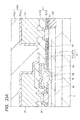
- FIG. 1 is a cross sectional view showing a configuration of the semiconductor device of the present embodiment.
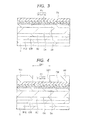
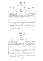
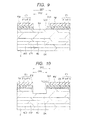
- FIGS. 2 to 17 are each a cross sectional view showing the semiconductor device of the present embodiment during a manufacturing step.
- the insulation film IF1 has an opening in an opening region OA1.
- the opening is provided in a region wider toward the drain electrode DE side than the trench T formation region (opening region OA2) by the distance Ld.
- the insulation film IF1 is set back from the end of the trench T on the drain electrode DE side by the distance Ld.
- the gate electrode GE has a shape projecting in one direction (the right-hand side in FIG. 1 , the drain electrode DE side).
- the projecting part is also referred to as a field plate electrode (which is also referred to as a field plate electrode part or a FP electrode part) FP.
- the field plate electrode FP is a partial region of the gate electrode GE extending from the end of the trench T on the drain electrode DE side toward the drain electrode DE side.
- an insulation film IF1 has a lamination structure of a Si-rich silicon nitride film IF1b, and a N-rich silicon nitride film IF1a situated thereunder.
- the insulation film IF1 has a N-rich silicon nitride film IF1a in contact with the barrier layer BA, and a Si-rich silicon nitride film IF1b situated thereover.
- the silicon nitride film IF1b is larger in composition ratio of silicon (Si) than the silicon nitride film IF1a.
- the N-rich silicon nitride film refers to that having a composition ratio [Si] / [N] of 0.85 or less.
- the Si-rich silicon nitride film refers to that having a composition ratio [Si]/[N] of larger than 0.85.
- the insulation film IF1 is arranged over the barrier layer BA on the opposite sides of the trench T. Further, over the insulation film IF1, a gate electrode GE is arranged via the gate insulation films GI. Then, a Si-rich silicon nitride film IF1b is arranged on the gate insulation film GI side. A N-rich silicon nitride film IF1a is arranged on the barrier layer BA side.
- the insulation film IF1 is formed in a lamination structure. This can improve the characteristics of the semiconductor device.
- FIGS. 2 to 17 are each a cross sectional view showing the semiconductor device of the present embodiment during a manufacturing step.
- the substrate S there are sequentially formed the nucleation layer NUC, the strain relaxation layer STR, and the buffer layer BU.
- the substrate S there is used, for example, a semiconductor substrate formed of silicon (Si) with a (111) -plane exposed.
- the nucleation layer NUC for example, an aluminum nitride (AlN) layer is heteroepitaxially grown using the metal organic chemical vapor deposition (MOCVD) method or the like.
- MOCVD metal organic chemical vapor deposition
- the buffer layer BU Over the strain relaxation layer STR, as the buffer layer BU, for example, an AlGaN layer is heteroepitaxially grown using the metal organic chemical vapor deposition method or the like.
- a N-rich silicon nitride film IF1a is deposited with a film thickness of, for example, about 30 nm using a CVD (Chemical Vapor Deposition) method or the like.
- a Si-rich silicon nitride film IF1b is deposited with a film thickness of, for example, about 60 nm using a CVD method or the like.
- the composition ratio of the silicon nitride film namely, whether the N-rich or Si-rich composition is achieved can be adjusted by changing the gas flow rate ratio of the raw material gas (i.e., a mixed gas of a silicon compound gas and a nitrogen compound gas) as described later. Then, over the insulation film IF1, as a masking insulation film IFM, for example, a silicon oxide film is formed using a CVD method.
- the raw material gas i.e., a mixed gas of a silicon compound gas and a nitrogen compound gas
- the photoresist film PR2 is removed.
- the insulation film IF1 having an opening in the opening region OA2.
- a masking insulation film IFM set back from one end of the opening region OA2, and having an opening in the opening region OA1.
- the insulation film IF1 is etched.
- the end of the insulation film IF1 on the trench T side is set back in one direction (the right-hand side in FIG. 11 ) by the distance Ld. This direction is the drain electrode DE side described later.
- the masking insulation film IFM is removed by etching.
- the gate insulation film GI there may be used a silicon oxide film or a high dielectric constant film higher in dielectric constant than a silicon oxide film other than alumina (alumina-containing film).
- the high dielectric constant film there may be used a hafnium oxide film (HfO 2 film).
- the high dielectric constant films there may be used other hafnium type insulation films such as a hafnium aluminate film, a HfON film (hafnium oxynitride film), a HfSiO film (hafnium silicate film), a HfSiON film (hafnium silicon oxynitride film), and a HfAlO film.
- a gate electrode GE over the gate insulation film GI in the inside of the trench T, there is formed a gate electrode GE.
- a conductive film for example, a TiN (titanium nitride) film is deposited using a sputtering method or the like. Then, using a photolithography technology and an etching technology, the TiN film and the alumina are patterned, thereby to form the gate electrode GE.
- the source electrode SE and the drain electrode DE are formed using, for example, a lift-off method.
- a photoresist film (not shown).
- a metal film is formed directly over the barrier layer BA.
- a metal film is formed over the photoresist film.
- the metal film is formed of, for example, an Al/Ti film.
- a lamination film formed of a titanium (Ti) film and an aluminum (Al) film thereover is deposited using a vapor deposition method or the like.
- a heat treatment at 550°C for about 30 minutes is performed.
- the contact at the interface between the metal film and a GaN type semiconductor becomes an ohmic contact.
- the Al/Ti film is left only in the formation regions of the source electrode SE and the drain electrode DE.
- an insulation layer IL1 Over the gate electrode GE, the insulation film IF1, and the barrier layer BA, as the insulation layer IL1, for example, a silicon oxide film is formed using a CVD method or the like. Then, using a photolithography technology and an etching technology, contact holes C1 are formed in the insulation layer IL1. The contact holes C1 are arranged over the source electrode SE and the drain electrode DE, respectively.
- an insulation layer (which is also referred to as a cover film or a surface protective film) IL2.
- a cover film or a surface protective film for example, a silicon oxynitride (SiON) film is deposited using a CVD method or the like.
- the insulation film IF1 is formed in a lamination structure of the Si-rich silicon nitride film IF1b, and the N-rich silicon nitride film IF1a situated thereunder.
- This can improve the characteristics of the semiconductor device. Specifically, as compared with a semiconductor device shown in FIG. 18 , the breakdown voltage can be improved. Further, the etching resistance can be improved. Still further, the collapse can be suppressed.
- FIG. 18 is a cross sectional view showing a configuration of a semiconductor device of Comparative Example.
- the insulation film (protective film) IF over the barrier layer BA is formed of a monolayered silicon nitride film.
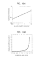
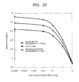
- FIG. 19A is a graph showing the relation between the gas flow rate ratio [NH 3 ]/[SiH 4 ] and the composition ratio [N]/[Si].
- the vertical axis represents the composition ratio [N] /[Si]
- the horizontal axis represents the gas flow rate ratio [NH 3 ]/[SiH 4 ].
- the wet etching rate is large. Further, the dry etching rate is also large. This indicates as follows: in either etching of wet etching and dry etching, the etching resistance is small. On the other hand, in the case of a Si-rich composition ratio of a composition ratio [Si] / [N] of 0.85 or more, the wet etching rate is small. Further, the dry etching rate is also small. This indicates as follows: in either etching of wet etching and dry etching, the etching resistance is large. Accordingly, by configuring the upper layer of the insulation film (protective film) IF1 as a Si-rich silicon nitride film IF1b, it is possible to improve the etching resistance.
- FIG. 25 is a cross sectional view showing a configuration of the semiconductor device studied in the present embodiment.
- the semiconductor device shown in FIG. 25 is a planar type FET not having a gate recess structure, and adopting a Schottky gate.
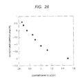
- FIG. 27 is a graph showing the relation between the composition ratio [Si] / [N] of the silicon nitride film and the current variation due to collapse of the semiconductor device of Type-I.
- the vertical axis represents the current variation [%] due to collapse, and the horizontal axis represents the composition ratio [Si]/[N].
- the composition ratio [Si]/[N] of the silicon nitride film affects the collapse characteristic. Then, for control of the collapse, it is most desirable to achieve a film composition in the vicinity of 0. 75 which is the stoichiometric composition ratio.
- the refractive index n of the silicon nitride film in this case is about 1.98.
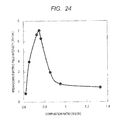
- a 1000-hour high-temperature operating test was performed on the semiconductor device of Type-I. Then, the variation of the saturated output power at 800 MHz, and a drain voltage (Vd) of 50 V was measured. The variation is the output power variation ( ⁇ Psat).
- the high-temperature operating test was performed under the conditions of a channel temperature of 250°C, a drain voltage (Vd) of 50 V, and a drain current of 50 mA/mm.
- the output power variation ( ⁇ Psat) is also referred to as a power slamp. It is assumed that an increase in the variation results in larger long-term fluctuations of the drain current, the threshold value, the breakdown voltage, and the like. For this reason, when the variation is small, the variation serves as an indicator indicating that the semiconductor device can operate stably even through a long-term use.
- the output power variation ( ⁇ Psat) becomes a minus value. Namely, this means that the output power decreases.
- Such an increase in output power variation (power ⁇ slamp) is presumably caused by the following: H (hydrogen) in the Si-H bond dissociates, and electrons in the semiconductor device are trapped by the dangling bond of Si.
- the output power variation ( ⁇ Psat) becomes a plus value. Namely, this means that the output power increases.
- the cause of the increase in the output power is a little increase in drain current. However, the details of the cause have not been able to be analyzed clearly.
- the film composition in the vicinity of 0.75 which is the stoichiometric composition ratio.
- the output power variation ( ⁇ Psat) of -0.5 or more can be ensured.
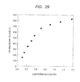
- FIG. 2 9 is a graph showing the relation between the composition ratio [Si] / [N] of the silicon nitride film and the off breakdown voltage of the semiconductor device of Type-I.
- the vertical axis represents the off breakdown voltage [V]
- the horizontal axis represents the composition ratio [Si] /[N].
- the off breakdown voltage is defined as the drain voltage (Vd) when a drain current (Ids) flows at 1 mA/mm.
- the off breakdown voltage increases.
- the composition ratio [Si]/[N] of the silicon nitride film exceeds 0.85, an off breakdown voltage of 650 V or more can be ensured.
- the composition ratio [Si] / [N] of the silicon nitride film it is preferable that 0.85 ⁇ [Si]/[N] ⁇ 1.6 is satisfied.
- the refractive index n it is preferable that 2.1 ⁇ n ⁇ 2.66 is satisfied.
- the breakdown voltage of the semiconductor device is improved.
- Lgs was set at 1 ⁇ m; Lg, 1 ⁇ m; Lgd, 2.5 ⁇ m; Lfp, 1 ⁇ m or 0; and Wg, 50 ⁇ m.
- the barrier layer BA AlGaN was used. The thickness was set at 30 nm, and the composition of Al was set at 25%.
- the insulation film IF1 the film thickness was 60 nm. The Si-rich silicon nitride film and the N-rich silicon nitride film were studied.
- the composition ratio [Si]/[N] is 0.95.
- the composition ratio [Si]/[N] is 0.75.
- the field plate electrodes (FP electrodes) the structure with a Lfp of 1 ⁇ m (with a FP electrode), and with a Lfp of 0 (without a FP electrode) were studied (see (a) to (d) of FIG. 30 ).
- the current variation due to collapse was 8%; the off breakdown voltage, 50 V; and the dry etching rate, 800 ⁇ /min.
- the configuration (d), namely, the configuration obtained by adding a FP electrode to the configuration (c) the current variation due to collapse was 4%; the off breakdown voltage, 190 V; and the dry etching rate, 800 ⁇ /min.
- the current variation due to collapse was 9%; the off breakdown voltage, 120 V; and the dry etching rate, 210 ⁇ /min.
- the configuration (f) namely, the configuration obtained by adding a FP electrode to the configuration (e)
- the current variation due to collapse was 1 to 3%; the off breakdown voltage, 210 V; and the dry etching rate, 210 ⁇ /min.
- FIG. 31 is a view schematically showing the electric field distribution in the case of a N-rich monolayer and with a FP electrode.
- FIG. 32 is a view schematically showing the electric field distribution in the case using a lamination film of the Si-rich silicon nitride film and the N-rich silicon nitride film, and with a FP electrode.
- the upper diagram is a cross sectional view in the vicinity of the FP electrode, in which an equipotential line is indicated with a broken line.
- the lower diagram is a graph showing the electric field intensity distribution between A-B of the cross sectional view.
- a lamination film of a Si-rich silicon nitride film and a N-rich silicon nitride film is used, and a FP electrode is applied. As a result, it is possible to improve the breakdown voltage of the semiconductor device.
- the Si-rich silicon nitride film is in direct contact with the field plate electrode FP.
- the Si-rich silicon nitride film is in contact with the field plate electrode FP via the gate insulation film GI, the same effects are produced. Namely, as shown in FIG. 1 , by using a lamination film of a Si-rich silicon nitride film and a N-rich silicon nitride film, and applying a FP electrode, it is possible to improve the breakdown voltage of the semiconductor device.
- the preferable range of the length (Lfp) of the field plate electrode will be studied from the viewpoints of the switching rate required of the semiconductor device, the driving loss, and the like.
- Cgd is the gate-drain capacity
- Cgs the gate-source capacity
- Cds the source-drain capacity.
- Each capacity has a non-linear voltage dependency. At a low voltage, the capacity value becomes large.
- the semiconductor device of the present embodiment includes the gate electrode GE insulated by the gate insulation film GI, and is a unipolar device. Accordingly, the switching mechanism is capable of high-speed operation because of no accumulation of minority carriers as distinct from a bipolar transistor.
- the MIS capacitor by the gate insulation film GI is charged, and the gate voltage Vg is set at a threshold voltage Vth or higher.
- the rate of switching the semiconductor device of the present embodiment is determined by the rate of charging and discharging the input capacity Ciss of the gate insulation film GI.
- the gate-drain capacity Cgd feedbacks the output waveform from the drain electrode DE to the input waveform to the gate electrode GE, the gate waveform, and adversely affects the input waveform.
- the gate-drain capacity Cgd which is the feedback capacity.
- the effects of the feedback capacity and the bias are added.
- an improvement of the switching rate requires the reduction of the parasitic capacity Cgd.
- the parasitic capacity Cgd it is effective to elongate the distance from the end of the FP electrode on the drain electrode DE side to the drain electrode DE.
- the gate-drain distance Lgd is preferably set at 1 ⁇ m or more.
- the length (Lfp) of the FP electrode is preferably longer than 0.5 ⁇ m.
- the upper limit of the length (Lfp) of the FP electrode is preferably set at ⁇ Lgd ( ⁇ m in unit) from the empirical rule.
- the length (Lfp, ⁇ m in unit) of the FP electrode preferably satisfies 0.5 ⁇ Lfp ⁇ ⁇ Lgd.
- FIG. 33A is a cross sectional view showing another configuration of the semiconductor device of the present embodiment.
- a nucleation layer (not shown), a strain relaxation layer (not shown), a buffer layer BU, a channel layer CH, and a barrier layer BA.
- a gate electrode GE is formed in the inside of a trench penetrating through an insulation film IF1 and the barrier layer BA, and reaching some point of the channel layer CH via a gate insulation film GI.
- the channel layer CH and the barrier layer BA are each formed of a nitride semiconductor.
- the barrier layer BA is a nitride semiconductor larger in band gap than the channel layer CH.
- the gate insulation film GI provided in such a manner as to be in contact with at least the Si-rich silicon nitride film IF1b.
- the gate electrode GE may be provided in such a manner as to be in contact with the Si-rich silicon nitride film IF1b (see FIG. 42 , and the like).
- the insulation layer IL1 is formed of a lamination film of a first layer IL1a and the overlying second layer IL1b.
- the first layer ILla is formed of a silicon nitride film with a film thickness of, for example, about 90 nm.
- the silicon nitride film is a stoichiometric composition film (N-rich silicon nitride film) with a composition ratio [Si]/[N] of about 0.75. Accordingly, the N-rich silicon nitride film (IL1a) covers the insulation film IF1.
- the N-rich silicon nitride film (IL1a) is provided over the gate electrode GE and the insulation film IF1, and is smaller in composition ratio of silicon (Si) than the Si-rich silicon nitride film IF1b. Further, over the N-rich silicon nitride film (IL1a), there is provided a second layer IL1b formed of a silicon oxide film.
- the protective film PRO is formed of a lamination film of a first layer PROa and a second layer PROb thereover.
- the first layer PROa is formed of, for example, a silicon oxynitride film.
- the second layer PROb is formed of, for example, a polyimide film.
- the gate electrode GE, the source electrode SE, and the drain electrode DE are formed in active regions defined by element isolation regions ISO.
- the element isolation region ISO is a region formed in the following manner: for example, ion species such as boron (B) and nitrogen (N) are implanted into the buffer layer BU, the channel layer CH, and the barrier layer BA, resulting in a change in crystal state, which leads to a higher resistance.
- a nucleation layer (not shown), a strain relaxation layer (not shown), and a buffer layer BU.
- a buffer layer BU in the same manner as with the semiconductor device shown in FIG. 1 , there are sequentially formed a channel layer CH and a barrier layer BA.
- an insulation film IF1 is formed over the barrier layer BA, in the same manner as with the semiconductor device shown in FIG. 1 .
- a N-rich silicon nitride film IF1a is deposited using a CVD method or the like.
- a Si-rich silicon nitride film IF1b is deposited using a CVD method or the like.
- the composition ratio of the silicon nitride film namely, whether the N-rich or Si-rich composition is achieved can be adjusted by changing the gas flow rate ratio of the raw material gas (i.e. , a mixed gas of a silicon compound gas and a nitrogen compound gas) as described previously.
- the insulation film IF1 and the barrier layer BA there is formed a trench penetrating through the insulation film IF1 and the barrier layer BA, and reaching some point of the channel layer CH. Further, over the insulation film IF1 including the inside of the trench and the exposed portions of the barrier layer BA, there are sequentially formed alumina to be the gate insulation film GI, and a TiN film to be the gate electrode GE. Then, the TiN film and alumina are etched, thereby to form the gate insulation film GI and the gate electrode GE.
- the insulation film IF1 is patterned, thereby to expose the portions of the barrier layer BA in the formation regions of the source electrode SE and the drain electrode DE.
- a metal film is deposited by a sputtering method or the like.
- the metal film is formed of, for example, an Al/Ti film.
- the metal film is patterned, thereby to form the source electrode SE and the drain electrode DE.
- a silicon nitride film is deposited with a film thickness of about 90 nm using a CVD method or the like.
- the silicon nitride film is a N-rich silicon nitride film with a composition ratio [Si]/[N] of about 0.75.
- a second layer IL1b is formed over the first layer IL1a.
- a silicon oxide film is deposited with a film thickness of about 500 nm using a plasma CVD method or the like.
- TEOS Tetra Ethyl Ortho Silicate
- contact holes are formed in the insulation layer IL1.
- the contact holes are arranged over the source electrode SE and the drain electrode DE, respectively.
- a protective film PRO For example, over the wire M1 and the insulation layer IL1, as a first layer PROa, a silicon oxynitride film is deposited using a CVD method or the like. Then, over the silicon oxynitride film, as a second layer PROb, there is formed a polyimide film. For example, over the silicon oxynitride film (PROa), a polyimide material is applied, and is subjected to a heat treatment, thereby to form a polyimide film. As a result, as the protective film PRO, it is possible to form a lamination film of the silicon oxynitride film (PROa), and the polyimide film (PROb) thereover.
- the insulation film IF1 is formed of the Si-rich silicon nitride film IF1b, and the N-rich silicon nitride film IF1a situated thereunder. For this reason, it is possible to improve the characteristics of the semiconductor device.
- the upper layer of the insulation film IF1 is formed of the Si-rich silicon nitride film IF1b. As a result, it is possible to improve the breakdown voltage.
- the lower layer of the insulation film IF1 is formed of the N-rich silicon nitride film IF1a. As a result, it is possible to suppress the collapse.
- Lgs is 1 ⁇ m; Lg, 1 ⁇ m; Lgd, 10 ⁇ m; and Lfp, 2.5 ⁇ m.
- barrier layer BA AlGaN is used as the barrier layer BA.
- the thickness is 30 nm, and the composition of Al is 25%.
- the upper layer of the insulation film IF1 is 20 nm in thickness, and the lower layer thereof is 40 nm in thickness.
- Other configurations are the same as those of the embodiment, and hence a description thereon is omitted.
- the insulation film IF1, the barrier layer BA, and the channel layer CH are etched.
- the trench T penetrating through the insulation film IF1 and the barrier layer BA, and reaching some point of the channel layer CH see FIG. 38 and the like of Second Embodiment described later.
- Other steps are the same as those of the embodiment, and hence a description thereon is omitted.
- FIG. 34 is a cross sectional view showing a configuration of Modified Example 2 of the semiconductor device of the present embodiment.
- the end of the insulation film IF1 on the drain electrode DE side is set back from the end of the trench T toward the drain electrode DE side by a set-back amount Ld. Further, the end of the insulation film IF1 on the source electrode SE side is set back from the end of the trench T toward the source electrode SE side by a set-back amount Ls.
- Other configurations are the same as those of the embodiment, and hence a description thereon is omitted.
- FIG. 35 is a cross sectional view showing a configuration of Modified Example 3 of the semiconductor device of the present embodiment.
- the angle (which is also referred to as a taper angle ⁇ ) formed between the side surface (sidewall) of the trench T and the extension surface of the bottom surface of the trench T is less than 90°.
- the angle formed between the side surface (sidewall) of the trench T and the (111) plane is less than 90°.
- Other configurations are the same as those in the embodiment, and hence a description thereon is omitted.
- a nucleation layer NUC As shown in FIG. 36 , also in the semiconductor device of the present embodiment, as with First Embodiment ( FIG. 1 ), over a substrate S, there are sequentially formed a nucleation layer NUC, a strain relaxation layer STR, a buffer layer BU, a channel layer CH, and a barrier layer BA.
- a gate electrode GE is formed in the inside of a trench T penetrating through an insulation film IF1 and the barrier layer BA, and reaching some point of the channel layer CH via a gate insulation film GI.
- the channel layer CH and the barrier layer BA are each formed of a nitride semiconductor and are each a nitride semiconductor larger in band gap than the channel layer CH.
- the insulation film IF1 is, as with First Embodiment, formed of a lamination film of a Si-rich silicon nitride film IF1b, and a N-rich silicon nitride film IF1a situated thereunder. Then, the insulation film IF1 has an opening (T) in the opening region OA2. In the outer circumferential part (outside) of the opening region OA2, there is arranged a lamination film of the gate electrode GE, the gate insulation film GI, and the insulation film IF1.
- the ends of the lamination film on the drain electrode DE side are nearly aligned.
- the ends on the source electrode SE side are also nearly aligned.
- the upper layer of the insulation film IF1 as the Si-rich silicon nitride film IF1b, it is possible to improve the breakdown voltage.
- the lower layer of the insulation film IF1 as the N-rich silicon nitride film IF1a, it is possible to suppress the collapse.
- the insulation film IF2 is formed of an insulation film such as a silicon nitride film or a silicon oxynitride film.
- the insulation film IF2 there is used a lamination film of a Si-rich silicon nitride film, and a N-rich silicon nitride film situated under the silicon nitride film, and smaller in composition ratio of silicon (Si) than the silicon nitride film.
- the N-rich silicon nitride film included in the insulation film IF2 is smaller in composition ratio of silicon (Si) than the Si-rich silicon nitride film IF1b provided thereunder.
- FIGS. 37 to 41 are each a cross sectional view showing the semiconductor device of the present embodiment during a manufacturing step.
- a nucleation layer NUC As shown in FIG. 37 , over a substrate S, in the same manner as with First Embodiment, there are sequentially formed a nucleation layer NUC, a strain relaxation layer STR, and a buffer layer BU. Then, over the buffer layer BU, in the same manner as with First Embodiment, the channel layer CH and the barrier layer BA are sequentially formed.
- an insulation film IF1 is formed over the barrier layer BA, in the same manner as with First Embodiment.
- a N-rich silicon nitride film IF1a is deposited using a CVD method or the like.
- a Si-rich silicon nitride film IF1b is deposited using a CVD method or the like.
- the composition ratio of the silicon nitride film namely, whether the N-rich or Si-rich composition is achieved can be adjusted by changing the gas flow rate ratio of the raw material gas (i.e., a mixed gas of silicon compound gas and a nitrogen compound gas) as described in First Embodiment.
- the insulation film IF1, the barrier layer BA, and the channel layer CH are etched.
- the trench T penetrating through the insulation film IF1 and the barrier layer BA, and reaching some point of the channel layer CH.
- a chlorine type gas such as BCl 3
- the photoresist film PR11 is removed.
- alumina to be the gate insulation film GI.
- a TiN film conductive film
- a photoresist film PR12 covering the opening region OA2 and its outer circumferential part. Then, using the photoresist film PR12 as a mask, the insulation film IF1, alumina to be the gate insulation film GI, and the conductive film to be the gate electrode GE are etched.
- the TiN film and alumina are subjected to dry etching by a chlorine type gas.
- the insulation film IF1 is subjected to dry etching by a fluorine type gas.
- the gate electrode GE is patterned in a shape projecting in one direction (the right-hand side in FIG. 39 , the drain electrode DE side). In other words, patterning is performed so as to provide a field plate electrode FP as a part of the gate electrode GE.
- a plasma peel treatment or the like the photoresist film PR12 is removed.
- an insulation film IF2 For example, as the insulation film IF2, a silicon nitride film is deposited using a CVD method or the like. As a result, the part between the trench T and the drain electrode DE is covered with the insulation films IF1 and IF2.
- the insulation film IF2 is patterned, thereby to expose the portions of the barrier layer BA in the formation regions of the source electrode SE and the drain electrode DE ( FIG. 41 ).
- a metal film is deposited by a sputtering method or the like.
- the metal film is formed of, for example, an Al/Ti film.
- a metal film E is patterned, thereby to form the source electrode SE and the drain electrode DE (see FIG. 36 ).
- the insulation film IF2 there is used a lamination film of a Si-rich silicon nitride film, and a N-rich silicon nitride film situated thereunder, the etching resistance can be improved in the patterning step.
- an insulation layer such as a silicon oxide film.
- a wire (M1) to be coupled with the source electrode SE or the drain electrode DE.
- the steps are examples, and the semiconductor device of the present embodiment may be manufactured by other steps than the foregoing steps.
- the upper layer of the insulation film IF1 is formed of the Si-rich silicon nitride film IF1b. As a result, it is possible to improve the breakdown voltage.
- the lower layer of the insulation film IF1 is formed of the N-rich silicon nitride film IF1a. As a result, it is possible to suppress the collapse.
- the composition ratio [Si] / [N] of the N-rich silicon nitride film IF1a is preferably set within the range of 0.65 or more and 0.85 or less. Further, the composition ratio [Si]/[N] is more preferably adjusted within the range of 0.75 ⁇ 1%. Further, for an improvement of the off breakdown voltage, the composition ratio [Si]/[N] of the Si-rich silicon nitride film IF1b is preferably set at larger than 0.85.
- FIG. 42 is a cross sectional view showing a configuration of a semiconductor device of the present embodiment.
- a nucleation layer NUC As shown in FIG. 42 , also in the semiconductor device of the present embodiment, as with First Embodiment ( FIG. 1 ), over a substrate S, there are sequentially formed a nucleation layer NUC, a strain relaxation layer STR, a buffer layer BU, a channel layer CH, and a barrier layer BA.
- a gate electrode GE is formed in a trench T penetrating through the barrier layer BA, and reaching some point of the channel layer CH via an insulation film IF1.
- the channel layer CH and the barrier layer BA are each formed of a nitride semiconductor.
- the barrier layer BA is a nitride semiconductor larger in band gap than the channel layer CH.
- the insulation film IF1 is, as with First Embodiment, formed of a lamination film of a Si-rich silicon nitride film IF1b, and a N-rich silicon nitride film IF1a situated thereunder.
- Lgs is 1 ⁇ m; Lg, 1 ⁇ m; Lgd, 10 ⁇ m; and Lfp, 2.5 ⁇ m.
- the barrier layer BA AlGaN is used as the barrier layer BA.
- the thickness is 30 nm, and the composition of Al is 25%.
- the upper layer of the insulation film IF1 is 30 nm in thickness, and the lower layer thereof is 30 nm in thickness.
- the insulation film IF1 is formed of a lamination film of the Si-rich silicon nitride film IF1b, and the N-rich silicon nitride film IF1a situated thereunder. For this reason, as described in details in First Embodiment, it is possible to improve the characteristics of the semiconductor device.
- the upper layer of the insulation film IF1 as the Si-rich silicon nitride film IF1b, it is possible to improve the breakdown voltage. Further, it is possible to improve the etching resistance. Whereas, by forming the lower layer of the insulation film IF1 as the N-rich silicon nitride film IF1a, it is possible to suppress the collapse.
- FIGS. 43 to 45 are each a cross sectional view showing the semiconductor device of the present embodiment during a manufacturing step.
- a nucleation layer NUC As shown in FIG. 43 , over a substrate S, in the same manner as with First Embodiment, there are sequentially formed a nucleation layer NUC, a strain relaxation layer STR, a buffer layer BU, a channel layer CH, and a barrier layer BA.
- a masking insulation film IFM for example, a silicon oxide film is formed. Then, using a photolithography technology and an etching technology, the insulation film IFM is patterned, thereby to form an opening in an opening region OA2.
- an insulation film IF1 is formed over the barrier layer BA including the inside of the trench T.
- a N-rich silicon nitride film IF1a is deposited using a CVD method or the like.
- a Si-rich silicon nitride film IF1b is deposited using a CVD method or the like.
- the source electrode SE and the drain electrode DE are, as with First Embodiment, formed using a lift-off method (see FIG. 42 ) .
- an insulation layer (IL1) there is formed a wire (M1) to be coupled with the source electrode SE or the drain electrode DE.
- the steps are examples, and the semiconductor device of the present embodiment may be manufactured by other steps than the foregoing steps.
- the insulation film IF1 is formed of the Si-rich silicon nitride film IF1b, and the N-rich silicon nitride film IF1a situated thereunder. As a result, it is possible to improve the characteristics of the semiconductor device.
- the upper layer of the insulation film IF1 is formed of the Si-rich silicon nitride film IF1b. As a result, it is possible to improve the breakdown voltage. Further, it is possible to improve the etching resistance.
- the lower layer of the insulation film IF1 is formed of the N-rich silicon nitride film IF1a. As a result, it is possible to suppress the collapse.
- the composition ratio [Si] / [N] of the N-rich silicon nitride film IF1a is preferably set within the range of 0.65 or more and 0.85 or less. Further, the composition ratio [Si]/[N] is more preferably adjusted within the range of 0.75 ⁇ 1% . Further, for an improvement of the off breakdown voltage, the composition ratio [Si]/[N] of the Si-rich silicon nitride film IF1b is preferably set at larger than 0.85.
- a nucleation layer NUC As shown in FIG. 46 , also in the semiconductor device of the present embodiment, as with First Embodiment ( FIG. 1 ), over a substrate S, there are sequentially formed a nucleation layer NUC, a strain relaxation layer STR, a buffer layer BU, a channel layer CH, and a barrier layer BA.
- a gate electrode GE is formed in the inside of a trench T penetrating through the insulation film IF1, and reaching some point of the barrier layer BA.
- the channel layer CH and the barrier layer BA are each formed of a nitride semiconductor.
- the barrier layer BA is a nitride semiconductor larger in band gap than the channel layer CH.
- the insulation film IF1 is, as with First Embodiment, formed of a lamination film of a Si-rich silicon nitride film IF1b, and a N-rich silicon nitride film IF1a situated thereunder.
- the insulation film IF1 is formed in a lamination structure of the Si-rich silicon nitride film IF1b, and the N-rich silicon nitride film IF1a situated thereunder. For this reason, as described in details in First Embodiment, it is possible to improve the characteristics of the semiconductor device.
- the upper layer of the insulation film IF1 as the Si-rich silicon nitride film IF1b, it is possible to improve the breakdown voltage.
- the lower layer of the insulation film IF1 as the N-rich silicon nitride film IF1a, it is possible to suppress the collapse.
- the trench T is not required to be formed.
- the formation of the trench T more suppresses the collapse, and facilitates the adjustment of the threshold voltage.
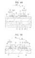
- FIGS. 47 to 49 are each a cross sectional view showing the semiconductor device of the present embodiment during a manufacturing step.
- a nucleation layer NUC As shown in FIG. 47 , over a substrate S, in the same manner as with First Embodiment, there are sequentially formed a nucleation layer NUC, a strain relaxation layer STR, a buffer layer BU, a channel layer CH, and a barrier layer BA.
- an insulation film IF1 is formed over the barrier layer BA.
- a N-rich silicon nitride film IF1a is deposited using a CVD method or the like.
- a Si-rich silicon nitride film IF1b is deposited using a CVD method or the like.
- the composition ratio of the silicon nitride film namely, whether the N-rich or Si-rich composition is achieved can be adjusted by changing the gas flow rate ratio of the raw material gas (i. e., a mixed gas of a silicon compound gas and a nitrogen compound gas) as described First Embodiment.
- the insulation film IF1 using a photolithography technology, there is formed a photoresist film (not shown) having an opening in an opening region OA2.
- a photoresist film (not shown) having an opening in an opening region OA2.
- the insulation film IF1 and the barrier layer BA are etched.
- the trench T penetrating through the insulation film IF1, and reaching some point of the barrier layer BA.
- the photoresist film is removed.
- a Tin film (conductive film) to be a gate electrode GE over the insulation film IF1 including the inside of the the trench T, there is formed a Tin film (conductive film) to be a gate electrode GE.
- a photoresist film PR2 covering an opening region OA2 and its outer circumferential part.
- the conductive film to be a gate electrode GE is etched.
- the TiN film is dry etched by a fluorine type gas.
- the photoresist film PR2 is removed by a plasma peel treatment or the like.
- the source electrode SE and the drain electrode DE are, as with First Embodiment, formed using a lift-off method (see FIG. 46 ).
- the insulation film IF1 is formed of the Si-rich silicon nitride film IF1b, and the N-rich silicon nitride film IF1a situated thereunder. For this reason, it is possible to improve the characteristics of the semiconductor device.
- the upper layer of the insulation film IF1 is formed of the Si-rich silicon nitride film IF1b. As a result, it is possible to improve the breakdown voltage. Further, it is possible to improve the etching resistance.
- the lower layer of the insulation film IF1 is formed of the N-rich silicon nitride film IF1a. As a result, it is possible to suppress the collapse.
- the composition ratio [Si] / [N] of the N-rich silicon nitride film IF1a is preferably set within the range of 0.65 or more and 0.85 or less. Further, the composition ratio [Si]/[N] is more preferably adjusted within the range of 0.75 ⁇ 1%. Further, for an improvement of the off breakdown voltage, the composition ratio [Si]/[N] of the Si-rich silicon nitride film IF1b is preferably set at larger than 0.85.
- the insulation film IF1 is, as with First Embodiment, formed in a lamination film of the Si-rich silicon nitride film IF1b, and the N-rich silicon nitride film IF1a situated thereunder.
- the insulation film IF1 is formed in a lamination structure of the Si-rich silicon nitride film IF1b, and the N-rich silicon nitride film IF1a situated thereunder. For this reason, as described in details in First Embodiment, it is possible to improve the characteristics of the semiconductor device.
- the upper layer of the insulation film IF1 is formed of the Si-rich silicon nitride film IF1b. As a result, it is possible to improve the breakdown voltage. Further, it is possible to improve the etching resistance.
- the lower layer of the insulation film IF1 is formed of the N-rich silicon nitride film IF1a. As a result, it is possible to suppress the collapse.
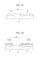
- FIGS. 51 to 54 are each a cross sectional view showing the semiconductor device of the present embodiment during a manufacturing step.
- the opening region OA2 of the channel layer CH of the substrate is covered with a mask film (not shown).
- n type impurities such as Si ions
- a heat treatment is performed at 1200°C for about 5 minutes.
- the mask film is removed.
- an insulation film IF1 is formed.
- a N-rich silicon nitride film IF1a is deposited using a CVD method or the like.
- a Si-rich silicon nitride film IF1b is deposited using a CVD method or the like.
- the composition ratio of the silicon nitride film namely, whether the N-rich or Si-rich composition is achieved can be adjusted by changing the gas flow rate ratio of the raw material gas (i.e. , a mixed gas of a silicon compound gas and a nitrogen compound gas) as described in First Embodiment.
- alumina to be a gate insulation film GI.
- a TiN film conductive film
- a photoresist film PR12 covering the opening region OA2 and its outer circumferential part.
- alumina to be the gate insulation film GI and the conductive film to be the gate electrode GE are etched.
- the TiN film and alumina are dry etched by a chlorine type gas.
- the gate electrode GE is patterned in a shape projecting in one direction (the right hand side in FIG. 53 , the drain electrode DE side). In other words, patterning is performed so as to provide a field plate electrode FP as a part of the gate electrode GE. Then, by a plasma peel treatment or the like, the photoresist film PR12 is removed.
- the insulation film IF1 is patterned.
- the insulation film IF1 is dry etched by a fluorine type gas. This results in exposure of the portions of the barrier layer BA in the formation regions of the source electrode SE and the drain electrode DE.
- the source electrode and the drain electrode there are formed the source electrode and the drain electrode. Further, over the gate electrode GE, the source electrode, and the drain electrode, there are formed insulation layers and wires.
- the steps are examples, and the semiconductor device of the present embodiment may be manufactured by other steps than the foregoing steps.
- the insulation film IF1 is formed of the Si-rich silicon nitride film IF1b, and the N-rich silicon nitride film IF1a situated thereunder. As a result, it is possible to improve the characteristics of the semiconductor device.
- the upper layer of the insulation film IF1 is formed of the Si-rich silicon nitride film IF1b. As a result, it is possible to improve the breakdown voltage. Further, it is possible to improve the etching resistance.
- the lower layer of the insulation film IF1 is formed of the N-rich silicon nitride film IF1a. As a result, it is possible to suppress the collapse.
- the composition ratio [Si] / [N] of the N-rich silicon nitride film IF1a is preferably set within the range of 0.65 or more and 0.85 or less. Further, the composition ratio [Si]/[N] is more preferably adjusted within the range of 0.75 ⁇ 1%. Further, for an improvement of the off breakdown voltage, the composition ratio [Si]/[N] of the Si-rich silicon nitride film IF1b is preferably set at larger than 0.85.
- the present invention made by the the present inventors was specifically described by way of embodiments. However, it is naturally understood that the present invention is not limited to the embodiments, and may be variously changed within the scope not departing from the gist thereof.
- the configuration of the insulation film IF2 of Second Embodiment may be applied to the semiconductor devices of Third to Fifth Embodiments.
- a semiconductor device including:
- a semiconductor device including:
- a semiconductor device including:
- a method for manufacturing a semiconductor device including the steps of:
- the characteristics of a semiconductor device are improved.
- a semiconductor device is formed so as to have a channel layer formed over a substrate, a barrier layer, a trench penetrating through the barrier layer in an opening region, and reaching some point of the channel layer, a gate electrode arranged in the trench via a gate insulation film, and an insulation film formed over the barrier layer outside the opening region.
- the insulation film has a lamination structure of a Si-rich silicon nitride film, and a N-rich silicon nitride film situated thereunder.
- the upper layer of the insulation film is set as the Si-rich silicon nitride film. This enables the improvement of the breakdown voltage, and further, enables the improvement of the etching resistance.
- the lower layer of the insulation film is set as the N-rich silicon nitride film. This can suppress collapse.
Landscapes
- Insulated Gate Type Field-Effect Transistor (AREA)
- Junction Field-Effect Transistors (AREA)
- Chemical & Material Sciences (AREA)
- Engineering & Computer Science (AREA)
- Ceramic Engineering (AREA)
- Electrodes Of Semiconductors (AREA)
- Formation Of Insulating Films (AREA)
Applications Claiming Priority (1)
| Application Number | Priority Date | Filing Date | Title |
|---|---|---|---|
| JP2013245845A JP6301640B2 (ja) | 2013-11-28 | 2013-11-28 | 半導体装置および半導体装置の製造方法 |
Publications (2)
| Publication Number | Publication Date |
|---|---|
| EP2879183A1 true EP2879183A1 (de) | 2015-06-03 |
| EP2879183B1 EP2879183B1 (de) | 2021-03-03 |
Family
ID=51846539
Family Applications (1)
| Application Number | Title | Priority Date | Filing Date |
|---|---|---|---|
| EP14191816.9A Active EP2879183B1 (de) | 2013-11-28 | 2014-11-05 | Halbleiterbauelement und Verfahren zur Herstellung eines Halbleiterbauelements |
Country Status (6)
| Country | Link |
|---|---|
| US (2) | US9306027B2 (de) |
| EP (1) | EP2879183B1 (de) |
| JP (1) | JP6301640B2 (de) |
| KR (1) | KR20150062135A (de) |
| CN (1) | CN104681617B (de) |
| TW (1) | TWI650863B (de) |
Cited By (2)
| Publication number | Priority date | Publication date | Assignee | Title |
|---|---|---|---|---|
| US11538919B2 (en) | 2021-02-23 | 2022-12-27 | Micron Technology, Inc. | Transistors and arrays of elevationally-extending strings of memory cells |
| WO2024039968A3 (en) * | 2022-08-18 | 2024-03-21 | Macom Technology Solutions Holdings, Inc. | High electron mobility transistors having improved passivation structures and reduces drain current drift, as well as methods of fabricating such devices |
Families Citing this family (38)
| Publication number | Priority date | Publication date | Assignee | Title |
|---|---|---|---|---|
| US9443737B2 (en) * | 2013-04-03 | 2016-09-13 | Texas Instruments Incorporated | Method of forming metal contacts in the barrier layer of a group III-N HEMT |
| JP6211804B2 (ja) * | 2013-05-30 | 2017-10-11 | トランスフォーム・ジャパン株式会社 | 半導体装置 |
| JP6220161B2 (ja) | 2013-06-03 | 2017-10-25 | ルネサスエレクトロニクス株式会社 | 半導体装置の製造方法 |
| JP6230456B2 (ja) * | 2014-03-19 | 2017-11-15 | 株式会社東芝 | 半導体装置 |
| US9761438B1 (en) * | 2014-05-08 | 2017-09-12 | Hrl Laboratories, Llc | Method for manufacturing a semiconductor structure having a passivated III-nitride layer |
| WO2016059889A1 (ja) * | 2014-10-14 | 2016-04-21 | シャープ株式会社 | 窒化物半導体装置 |
| KR102334110B1 (ko) * | 2014-10-24 | 2021-12-02 | 삼성전자주식회사 | 반도체 소자 형성방법 |
| JP6591168B2 (ja) * | 2015-02-04 | 2019-10-16 | 株式会社東芝 | 半導体装置及びその製造方法 |
| JP6530210B2 (ja) * | 2015-03-24 | 2019-06-12 | 株式会社東芝 | 半導体装置及びその製造方法 |
| WO2017033768A1 (ja) * | 2015-08-21 | 2017-03-02 | シャープ株式会社 | 光電変換素子及び光電変換モジュール |
| JPWO2017038139A1 (ja) * | 2015-08-28 | 2018-04-12 | シャープ株式会社 | 窒化物半導体装置 |
| JP6536318B2 (ja) | 2015-09-24 | 2019-07-03 | 三菱電機株式会社 | 半導体装置及びその製造方法 |
| US9799645B2 (en) * | 2015-11-20 | 2017-10-24 | Raytheon Company | Field effect transistor (FET) structure with integrated gate connected diodes |
| ITUB20155862A1 (it) * | 2015-11-24 | 2017-05-24 | St Microelectronics Srl | Transistore di tipo normalmente spento con ridotta resistenza in stato acceso e relativo metodo di fabbricazione |
| EP3179515A1 (de) * | 2015-12-10 | 2017-06-14 | Nexperia B.V. | Halbleiterbauelement und verfahren zur herstellung eines halbleiterbauelements |
| WO2017201063A1 (en) * | 2016-05-16 | 2017-11-23 | The Government Of The United States Of America, As Represented By The Secretary Of The Navy | Metal nitride alloy contact for semiconductor |
| EP3459118A4 (de) * | 2016-05-17 | 2020-01-15 | The Government Of The United States Of America As The Secretary of The Navy | Beschädigungsfreie, plasmaunterstützte cvd-passivierung von algan/gan-transistoren mit hoher elektronenmobilität |
| US9741557B1 (en) * | 2016-06-23 | 2017-08-22 | Texas Instruments Incorporated | Silicon nitride process for reduction of threshold shift |
| JP6677114B2 (ja) * | 2016-07-19 | 2020-04-08 | 豊田合成株式会社 | 半導体装置およびその製造方法 |
| CN107768248A (zh) * | 2016-08-19 | 2018-03-06 | 中国科学院苏州纳米技术与纳米仿生研究所 | GaN基增强型HEMT器件的制备方法 |
| US9865455B1 (en) * | 2016-09-07 | 2018-01-09 | Lam Research Corporation | Nitride film formed by plasma-enhanced and thermal atomic layer deposition process |
| JP2018094844A (ja) * | 2016-12-15 | 2018-06-21 | キヤノン株式会社 | パターン状膜の形成方法 |
| JP6629252B2 (ja) * | 2017-02-01 | 2020-01-15 | 株式会社東芝 | 半導体装置の製造方法 |
| JP6917160B2 (ja) * | 2017-02-26 | 2021-08-11 | 住友化学株式会社 | 半導体基板、電子デバイス、半導体基板の検査方法および電子デバイスの製造方法 |
| CN111969048B (zh) * | 2017-06-23 | 2023-05-02 | 深圳市晶相技术有限公司 | 氮化镓半导体功率器件及其制备方法 |
| US10446681B2 (en) | 2017-07-10 | 2019-10-15 | Micron Technology, Inc. | NAND memory arrays, and devices comprising semiconductor channel material and nitrogen |
| JP2019033204A (ja) * | 2017-08-09 | 2019-02-28 | ルネサスエレクトロニクス株式会社 | 半導体装置の製造方法および半導体装置 |
| CN109659361B (zh) * | 2017-10-12 | 2022-03-04 | 电力集成公司 | 用于异质结器件的栅极堆叠体 |
| US11121229B2 (en) | 2017-12-28 | 2021-09-14 | Vanguard International Semiconductor Corporation | Methods of fabricating semiconductor structures and high electron mobility transistors |
| JP7170433B2 (ja) | 2018-06-19 | 2022-11-14 | 株式会社東芝 | 半導体装置及びその製造方法 |
| JP7055533B2 (ja) | 2018-07-23 | 2022-04-18 | 株式会社東芝 | 半導体装置及びその製造方法 |
| JP2021089977A (ja) * | 2019-12-04 | 2021-06-10 | 富士通株式会社 | 半導体装置、半導体装置の製造方法及び増幅器 |
| JP7443788B2 (ja) * | 2020-01-24 | 2024-03-06 | 富士通株式会社 | 半導体装置 |
| JP7498906B2 (ja) * | 2020-02-26 | 2024-06-13 | 国立大学法人東海国立大学機構 | 電界効果トランジスタおよび電界効果トランジスタの製造方法 |
| US12349386B2 (en) | 2021-01-20 | 2025-07-01 | Kabushiki Kaisha Toshiba | Semiconductor device and method for manufacturing the same |
| CN115458580B (zh) | 2021-06-08 | 2025-12-09 | 株式会社东芝 | 半导体装置 |
| CN117116982A (zh) * | 2022-05-16 | 2023-11-24 | 联华电子股份有限公司 | 化合物半导体器件及其制作方法 |
| JP7805321B2 (ja) * | 2023-01-17 | 2026-01-23 | 株式会社東芝 | 半導体装置 |
Citations (5)
| Publication number | Priority date | Publication date | Assignee | Title |
|---|---|---|---|---|
| US20080035934A1 (en) * | 2005-06-29 | 2008-02-14 | Sheppard Scott T | Passivation of Wide Band-Gap Based Semiconductor Devices with Hydrogen-Free Sputtered Nitrides |
| JP2008205392A (ja) | 2007-02-22 | 2008-09-04 | Fujitsu Ltd | 半導体装置及びその製造方法 |
| JP2010206110A (ja) | 2009-03-05 | 2010-09-16 | Panasonic Corp | 窒化物半導体装置 |
| JP2012044003A (ja) | 2010-08-19 | 2012-03-01 | Toshiba Corp | 半導体装置及びその製造方法 |
| EP2575180A2 (de) * | 2011-09-29 | 2013-04-03 | Fujitsu Limited | Verbundhalbleiterbauelement und Herstellungsverfahren dafür |
Family Cites Families (10)
| Publication number | Priority date | Publication date | Assignee | Title |
|---|---|---|---|---|
| JP2725592B2 (ja) * | 1994-03-30 | 1998-03-11 | 日本電気株式会社 | 電界効果トランジスタの製造方法 |
| US7709269B2 (en) * | 2006-01-17 | 2010-05-04 | Cree, Inc. | Methods of fabricating transistors including dielectrically-supported gate electrodes |
| US7800116B2 (en) * | 2007-03-29 | 2010-09-21 | Panasonic Corporation | Group III-nitride semiconductor device with a cap layer |
| JP4719210B2 (ja) * | 2007-12-28 | 2011-07-06 | 富士通株式会社 | 半導体装置及びその製造方法 |
| US9711633B2 (en) * | 2008-05-09 | 2017-07-18 | Cree, Inc. | Methods of forming group III-nitride semiconductor devices including implanting ions directly into source and drain regions and annealing to activate the implanted ions |
| JP2011204780A (ja) * | 2010-03-24 | 2011-10-13 | Toshiba Corp | 半導体装置 |
| JP5878317B2 (ja) * | 2011-08-08 | 2016-03-08 | ルネサスエレクトロニクス株式会社 | 半導体装置及び半導体装置の製造方法 |
| JP5970775B2 (ja) * | 2011-10-31 | 2016-08-17 | 株式会社豊田中央研究所 | 保護素子、半導体装置及び半導体装置の製造方法 |
| JP5717677B2 (ja) * | 2012-03-06 | 2015-05-13 | 株式会社東芝 | 半導体装置およびその製造方法 |
| JP6054621B2 (ja) * | 2012-03-30 | 2016-12-27 | トランスフォーム・ジャパン株式会社 | 化合物半導体装置及びその製造方法 |
-
2013
- 2013-11-28 JP JP2013245845A patent/JP6301640B2/ja active Active
-
2014
- 2014-11-05 EP EP14191816.9A patent/EP2879183B1/de active Active
- 2014-11-11 TW TW103139037A patent/TWI650863B/zh active
- 2014-11-20 US US14/548,527 patent/US9306027B2/en active Active
- 2014-11-25 KR KR1020140165572A patent/KR20150062135A/ko not_active Withdrawn
- 2014-11-28 CN CN201410709104.XA patent/CN104681617B/zh active Active
-
2016
- 2016-03-24 US US15/079,879 patent/US9660045B2/en active Active
Patent Citations (6)
| Publication number | Priority date | Publication date | Assignee | Title |
|---|---|---|---|---|
| US20080035934A1 (en) * | 2005-06-29 | 2008-02-14 | Sheppard Scott T | Passivation of Wide Band-Gap Based Semiconductor Devices with Hydrogen-Free Sputtered Nitrides |
| JP2008205392A (ja) | 2007-02-22 | 2008-09-04 | Fujitsu Ltd | 半導体装置及びその製造方法 |
| JP2010206110A (ja) | 2009-03-05 | 2010-09-16 | Panasonic Corp | 窒化物半導体装置 |
| JP2012044003A (ja) | 2010-08-19 | 2012-03-01 | Toshiba Corp | 半導体装置及びその製造方法 |
| EP2575180A2 (de) * | 2011-09-29 | 2013-04-03 | Fujitsu Limited | Verbundhalbleiterbauelement und Herstellungsverfahren dafür |
| JP2013077629A (ja) | 2011-09-29 | 2013-04-25 | Fujitsu Ltd | 化合物半導体装置及びその製造方法 |
Non-Patent Citations (5)
| Title |
|---|
| F. KAROUTA ET AL.: "Influence of the Structural and Compositional Properties of PECVD Silicon Nitride Layers on the Passivation of AlGaN/GaN HEMT", ECS TRANSACTIONS, vol. 16, no. 7, 2008, pages 181 - 191 |
| K. B. LEE ET AL.: "Bi-layer SixNy passivation on AlGaN/GaN HEMTs to suppress current collapse and improve breakdown", 2010 SEMICOND. SCI. TECHNOL., vol. 25, 2010, pages 125010, XP020201182, DOI: doi:10.1088/0268-1242/25/12/125010 |
| K. B. LEE ET AL.: "Bi-layer SixNy passivation on AlGaN/GaN HEMTs to suppress current collapse and improve breakdown", SEMICOND. SCI. TECHNOL., vol. 25, 125010, 16 November 2010 (2010-11-16), pages 1 - 5, XP002737833 * |
| T. MARUI ET AL.: "Effects of a Thermal CVD SiN Passivation Film on AlGaN/GaN HEMTs", 11 IEICE ELECTRON., vol. E91-C, no. 7, July 2008 (2008-07-01), pages 1009 - 1014 |
| WAKI EIJI ET AL.: "ECR sputtered SiN film quality effects on the characteristics of SiN/AlGaN/GaN MIS-HFETs", TECHNICAL MEETING OF THE INSTITUTE OF ELECTRICAL ENGINEERS OF JAPAN, TECHNICAL GROUP ON ELECTRON DEVICES, EDD11043, 2 March 2011 (2011-03-02) |
Cited By (4)
| Publication number | Priority date | Publication date | Assignee | Title |
|---|---|---|---|---|
| US11538919B2 (en) | 2021-02-23 | 2022-12-27 | Micron Technology, Inc. | Transistors and arrays of elevationally-extending strings of memory cells |
| US12170324B2 (en) | 2021-02-23 | 2024-12-17 | Lodestar Licensing Group Llc | Transistors and arrays of elevationally-extending strings of memory cells |
| WO2024039968A3 (en) * | 2022-08-18 | 2024-03-21 | Macom Technology Solutions Holdings, Inc. | High electron mobility transistors having improved passivation structures and reduces drain current drift, as well as methods of fabricating such devices |
| US12464759B2 (en) | 2022-08-18 | 2025-11-04 | Macom Technology Solutions Holdings, Inc. | High electron mobility transistors having reduced drain current drift and methods of fabricating such devices |
Also Published As
| Publication number | Publication date |
|---|---|
| US20160204243A1 (en) | 2016-07-14 |
| US9306027B2 (en) | 2016-04-05 |
| US9660045B2 (en) | 2017-05-23 |
| CN104681617A (zh) | 2015-06-03 |
| US20150145004A1 (en) | 2015-05-28 |
| TW201533900A (zh) | 2015-09-01 |
| EP2879183B1 (de) | 2021-03-03 |
| CN104681617B (zh) | 2020-02-18 |
| JP6301640B2 (ja) | 2018-03-28 |
| JP2015103780A (ja) | 2015-06-04 |
| KR20150062135A (ko) | 2015-06-05 |
| TWI650863B (zh) | 2019-02-11 |
Similar Documents
| Publication | Publication Date | Title |
|---|---|---|
| EP2879183B1 (de) | Halbleiterbauelement und Verfahren zur Herstellung eines Halbleiterbauelements | |
| Zhang et al. | Studies on high-voltage GaN-on-Si MIS-HEMTs using LPCVD Si 3 N 4 as gate dielectric and passivation layer | |
| Tang et al. | High-voltage (600-V) low-leakage low-current-collapse AlGaN/GaN HEMTs with AlN/SiN x passivation | |
| US12112945B2 (en) | Semiconductor wafer, electronic device, method of performing inspection on semiconductor wafer, and method of manufacturing electronic device | |
| US8912571B2 (en) | Compound semiconductor device including first film on compound semiconductor layer and second film on first film and method of manufacturing the same | |
| US9633920B2 (en) | Low damage passivation layer for III-V based devices | |
| JP6004319B2 (ja) | 半導体装置および半導体装置の製造方法 | |
| Ando et al. | Impact of film stress of field-plate dielectric on electric characteristics of GaN-HEMTs | |
| Cheng et al. | Comparative study on performance of AlGaN/GaN MS-HEMTs with SiNx, SiOx, and SiNO surface passivation | |
| Tilak et al. | Effect of passivation on AlGaN/GaN HEMT device performance | |
| Subhani et al. | Nitrogen rich PECVD silicon nitride for passivation of Si and AlGaN/GaN HEMT devices | |
| Cheng et al. | Improving the drive current of AlGaN/GaN HEMT using external strain engineering | |
| Chen et al. | Improved electrical performance of InAlN/GaN high electron mobility transistors with forming gas annealing | |
| US11695040B2 (en) | Self-aligned gate and drift design for high-critical field strength semiconductor power transistors with ion implantation | |
| Fregolent et al. | Systematic analysis of the trapping and reliability of Al2O3/GaN MOS capacitors with different atomic layer deposition techniques | |
| Iqbal et al. | Hot-electron reliability improvement using perhydropolysilazane spin-on-dielectric passivation buffer layers for AlGaN/GaN HEMTs | |
| Ding et al. | Effect of fluorinated graphene insulator on AlGaN/GaN MIS-HEMTs as gate dielectric | |
| Huang et al. | Analysis of the Extraction Method and Mechanism of Hot Carrier Degradation in Al 2 O 3/Si 3 N 4 Bilayer Gate Dielectric AlGaN/GaN MIS-HEMTs | |
| Kumar et al. | Performance analysis of GaN/AlGaN HEMTs passivation using inductively coupled plasma chemical vapour deposition and plasma enhanced chemical vapour deposition techniques | |
| Azam et al. | Optimization of ALD high-k gate dielectric to improve AlGaN/GaN MOS-HFET DC characteristics and reliability | |
| Kemmerling | The development of gallium nitride super-heterojunction transistors for 10-kV blocking and 3-kV switching | |
| Gao et al. | Single-step electron beam evaporation for integrated dual-metal gate and gate field-plate in GaN-on-Si MIS-HEMTs | |
| Kajiwara et al. | Suppression of current collapse by Access-region Carrier Enhancement technique in GaN-MOSFETs | |
| Feng et al. | Electrical characteristics of AlGaN/GaN metal-insulator-semiconductor high electron mobility transistor using La2O3 gate dielectric | |
| Hu et al. | Improved Low-Frequency Noise in Recessed-Gate E-Mode AlGaN/GaN MOS-HEMTs Under Electrical and Thermal Stress |
Legal Events
| Date | Code | Title | Description |
|---|---|---|---|
| PUAI | Public reference made under article 153(3) epc to a published international application that has entered the european phase |
Free format text: ORIGINAL CODE: 0009012 |
|
| 17P | Request for examination filed |
Effective date: 20141105 |
|
| AK | Designated contracting states |
Kind code of ref document: A1 Designated state(s): AL AT BE BG CH CY CZ DE DK EE ES FI FR GB GR HR HU IE IS IT LI LT LU LV MC MK MT NL NO PL PT RO RS SE SI SK SM TR |
|
| AX | Request for extension of the european patent |
Extension state: BA ME |
|
| RAP1 | Party data changed (applicant data changed or rights of an application transferred) |
Owner name: RENESAS ELECTRONICS CORPORATION |
|
| R17P | Request for examination filed (corrected) |
Effective date: 20151203 |
|
| RBV | Designated contracting states (corrected) |
Designated state(s): AL AT BE BG CH CY CZ DE DK EE ES FI FR GB GR HR HU IE IS IT LI LT LU LV MC MK MT NL NO PL PT RO RS SE SI SK SM TR |
|
| STAA | Information on the status of an ep patent application or granted ep patent |
Free format text: STATUS: EXAMINATION IS IN PROGRESS |
|
| 17Q | First examination report despatched |
Effective date: 20200203 |
|
| REG | Reference to a national code |
Ref country code: DE Ref legal event code: R079 Ref document number: 602014075321 Country of ref document: DE Free format text: PREVIOUS MAIN CLASS: H01L0029778000 Ipc: H01L0029660000 |
|
| RIC1 | Information provided on ipc code assigned before grant |
Ipc: H01L 29/20 20060101ALI20200625BHEP Ipc: H01L 29/66 20060101AFI20200625BHEP Ipc: H01L 29/778 20060101ALI20200625BHEP Ipc: H01L 29/423 20060101ALI20200625BHEP |
|
| GRAP | Despatch of communication of intention to grant a patent |
Free format text: ORIGINAL CODE: EPIDOSNIGR1 |
|
| STAA | Information on the status of an ep patent application or granted ep patent |
Free format text: STATUS: GRANT OF PATENT IS INTENDED |
|
| INTG | Intention to grant announced |
Effective date: 20200921 |
|
| GRAS | Grant fee paid |
Free format text: ORIGINAL CODE: EPIDOSNIGR3 |
|
| GRAA | (expected) grant |
Free format text: ORIGINAL CODE: 0009210 |
|
| STAA | Information on the status of an ep patent application or granted ep patent |
Free format text: STATUS: THE PATENT HAS BEEN GRANTED |
|
| AK | Designated contracting states |
Kind code of ref document: B1 Designated state(s): AL AT BE BG CH CY CZ DE DK EE ES FI FR GB GR HR HU IE IS IT LI LT LU LV MC MK MT NL NO PL PT RO RS SE SI SK SM TR |
|
| REG | Reference to a national code |
Ref country code: GB Ref legal event code: FG4D |
|
| REG | Reference to a national code |
Ref country code: AT Ref legal event code: REF Ref document number: 1368163 Country of ref document: AT Kind code of ref document: T Effective date: 20210315 Ref country code: CH Ref legal event code: EP |
|
| REG | Reference to a national code |
Ref country code: DE Ref legal event code: R096 Ref document number: 602014075321 Country of ref document: DE |
|
| REG | Reference to a national code |
Ref country code: IE Ref legal event code: FG4D |
|
| REG | Reference to a national code |
Ref country code: LT Ref legal event code: MG9D |
|
| PG25 | Lapsed in a contracting state [announced via postgrant information from national office to epo] |
Ref country code: BG Free format text: LAPSE BECAUSE OF FAILURE TO SUBMIT A TRANSLATION OF THE DESCRIPTION OR TO PAY THE FEE WITHIN THE PRESCRIBED TIME-LIMIT Effective date: 20210603 Ref country code: NO Free format text: LAPSE BECAUSE OF FAILURE TO SUBMIT A TRANSLATION OF THE DESCRIPTION OR TO PAY THE FEE WITHIN THE PRESCRIBED TIME-LIMIT Effective date: 20210603 Ref country code: HR Free format text: LAPSE BECAUSE OF FAILURE TO SUBMIT A TRANSLATION OF THE DESCRIPTION OR TO PAY THE FEE WITHIN THE PRESCRIBED TIME-LIMIT Effective date: 20210303 Ref country code: GR Free format text: LAPSE BECAUSE OF FAILURE TO SUBMIT A TRANSLATION OF THE DESCRIPTION OR TO PAY THE FEE WITHIN THE PRESCRIBED TIME-LIMIT Effective date: 20210604 Ref country code: FI Free format text: LAPSE BECAUSE OF FAILURE TO SUBMIT A TRANSLATION OF THE DESCRIPTION OR TO PAY THE FEE WITHIN THE PRESCRIBED TIME-LIMIT Effective date: 20210303 Ref country code: LT Free format text: LAPSE BECAUSE OF FAILURE TO SUBMIT A TRANSLATION OF THE DESCRIPTION OR TO PAY THE FEE WITHIN THE PRESCRIBED TIME-LIMIT Effective date: 20210303 |
|
| REG | Reference to a national code |
Ref country code: NL Ref legal event code: MP Effective date: 20210303 |
|
| REG | Reference to a national code |
Ref country code: AT Ref legal event code: MK05 Ref document number: 1368163 Country of ref document: AT Kind code of ref document: T Effective date: 20210303 |
|
| PG25 | Lapsed in a contracting state [announced via postgrant information from national office to epo] |
Ref country code: SE Free format text: LAPSE BECAUSE OF FAILURE TO SUBMIT A TRANSLATION OF THE DESCRIPTION OR TO PAY THE FEE WITHIN THE PRESCRIBED TIME-LIMIT Effective date: 20210303 Ref country code: RS Free format text: LAPSE BECAUSE OF FAILURE TO SUBMIT A TRANSLATION OF THE DESCRIPTION OR TO PAY THE FEE WITHIN THE PRESCRIBED TIME-LIMIT Effective date: 20210303 Ref country code: LV Free format text: LAPSE BECAUSE OF FAILURE TO SUBMIT A TRANSLATION OF THE DESCRIPTION OR TO PAY THE FEE WITHIN THE PRESCRIBED TIME-LIMIT Effective date: 20210303 Ref country code: PL Free format text: LAPSE BECAUSE OF FAILURE TO SUBMIT A TRANSLATION OF THE DESCRIPTION OR TO PAY THE FEE WITHIN THE PRESCRIBED TIME-LIMIT Effective date: 20210303 |
|
| PG25 | Lapsed in a contracting state [announced via postgrant information from national office to epo] |
Ref country code: NL Free format text: LAPSE BECAUSE OF FAILURE TO SUBMIT A TRANSLATION OF THE DESCRIPTION OR TO PAY THE FEE WITHIN THE PRESCRIBED TIME-LIMIT Effective date: 20210303 |
|
| PG25 | Lapsed in a contracting state [announced via postgrant information from national office to epo] |
Ref country code: AT Free format text: LAPSE BECAUSE OF FAILURE TO SUBMIT A TRANSLATION OF THE DESCRIPTION OR TO PAY THE FEE WITHIN THE PRESCRIBED TIME-LIMIT Effective date: 20210303 Ref country code: EE Free format text: LAPSE BECAUSE OF FAILURE TO SUBMIT A TRANSLATION OF THE DESCRIPTION OR TO PAY THE FEE WITHIN THE PRESCRIBED TIME-LIMIT Effective date: 20210303 Ref country code: CZ Free format text: LAPSE BECAUSE OF FAILURE TO SUBMIT A TRANSLATION OF THE DESCRIPTION OR TO PAY THE FEE WITHIN THE PRESCRIBED TIME-LIMIT Effective date: 20210303 Ref country code: SM Free format text: LAPSE BECAUSE OF FAILURE TO SUBMIT A TRANSLATION OF THE DESCRIPTION OR TO PAY THE FEE WITHIN THE PRESCRIBED TIME-LIMIT Effective date: 20210303 |
|
| PG25 | Lapsed in a contracting state [announced via postgrant information from national office to epo] |
Ref country code: IS Free format text: LAPSE BECAUSE OF FAILURE TO SUBMIT A TRANSLATION OF THE DESCRIPTION OR TO PAY THE FEE WITHIN THE PRESCRIBED TIME-LIMIT Effective date: 20210703 Ref country code: RO Free format text: LAPSE BECAUSE OF FAILURE TO SUBMIT A TRANSLATION OF THE DESCRIPTION OR TO PAY THE FEE WITHIN THE PRESCRIBED TIME-LIMIT Effective date: 20210303 Ref country code: SK Free format text: LAPSE BECAUSE OF FAILURE TO SUBMIT A TRANSLATION OF THE DESCRIPTION OR TO PAY THE FEE WITHIN THE PRESCRIBED TIME-LIMIT Effective date: 20210303 Ref country code: PT Free format text: LAPSE BECAUSE OF FAILURE TO SUBMIT A TRANSLATION OF THE DESCRIPTION OR TO PAY THE FEE WITHIN THE PRESCRIBED TIME-LIMIT Effective date: 20210705 Ref country code: ES Free format text: LAPSE BECAUSE OF FAILURE TO SUBMIT A TRANSLATION OF THE DESCRIPTION OR TO PAY THE FEE WITHIN THE PRESCRIBED TIME-LIMIT Effective date: 20210303 |
|
| REG | Reference to a national code |
Ref country code: DE Ref legal event code: R097 Ref document number: 602014075321 Country of ref document: DE |
|
| PLBE | No opposition filed within time limit |
Free format text: ORIGINAL CODE: 0009261 |
|
| STAA | Information on the status of an ep patent application or granted ep patent |
Free format text: STATUS: NO OPPOSITION FILED WITHIN TIME LIMIT |
|
| PG25 | Lapsed in a contracting state [announced via postgrant information from national office to epo] |
Ref country code: AL Free format text: LAPSE BECAUSE OF FAILURE TO SUBMIT A TRANSLATION OF THE DESCRIPTION OR TO PAY THE FEE WITHIN THE PRESCRIBED TIME-LIMIT Effective date: 20210303 Ref country code: DK Free format text: LAPSE BECAUSE OF FAILURE TO SUBMIT A TRANSLATION OF THE DESCRIPTION OR TO PAY THE FEE WITHIN THE PRESCRIBED TIME-LIMIT Effective date: 20210303 |
|
| 26N | No opposition filed |
Effective date: 20211206 |
|
| PG25 | Lapsed in a contracting state [announced via postgrant information from national office to epo] |
Ref country code: SI Free format text: LAPSE BECAUSE OF FAILURE TO SUBMIT A TRANSLATION OF THE DESCRIPTION OR TO PAY THE FEE WITHIN THE PRESCRIBED TIME-LIMIT Effective date: 20210303 |
|
| PG25 | Lapsed in a contracting state [announced via postgrant information from national office to epo] |
Ref country code: IT Free format text: LAPSE BECAUSE OF FAILURE TO SUBMIT A TRANSLATION OF THE DESCRIPTION OR TO PAY THE FEE WITHIN THE PRESCRIBED TIME-LIMIT Effective date: 20210303 |
|
| PG25 | Lapsed in a contracting state [announced via postgrant information from national office to epo] |
Ref country code: IS Free format text: LAPSE BECAUSE OF FAILURE TO SUBMIT A TRANSLATION OF THE DESCRIPTION OR TO PAY THE FEE WITHIN THE PRESCRIBED TIME-LIMIT Effective date: 20210703 |
|
| PG25 | Lapsed in a contracting state [announced via postgrant information from national office to epo] |
Ref country code: MC Free format text: LAPSE BECAUSE OF FAILURE TO SUBMIT A TRANSLATION OF THE DESCRIPTION OR TO PAY THE FEE WITHIN THE PRESCRIBED TIME-LIMIT Effective date: 20210303 |
|
| REG | Reference to a national code |
Ref country code: CH Ref legal event code: PL |
|
| GBPC | Gb: european patent ceased through non-payment of renewal fee |
Effective date: 20211105 |
|
| PG25 | Lapsed in a contracting state [announced via postgrant information from national office to epo] |
Ref country code: LU Free format text: LAPSE BECAUSE OF NON-PAYMENT OF DUE FEES Effective date: 20211105 Ref country code: BE Free format text: LAPSE BECAUSE OF NON-PAYMENT OF DUE FEES Effective date: 20211130 |
|
| REG | Reference to a national code |
Ref country code: BE Ref legal event code: MM Effective date: 20211130 |
|
| PG25 | Lapsed in a contracting state [announced via postgrant information from national office to epo] |
Ref country code: LI Free format text: LAPSE BECAUSE OF NON-PAYMENT OF DUE FEES Effective date: 20211130 Ref country code: CH Free format text: LAPSE BECAUSE OF NON-PAYMENT OF DUE FEES Effective date: 20211130 |
|
| PG25 | Lapsed in a contracting state [announced via postgrant information from national office to epo] |
Ref country code: IE Free format text: LAPSE BECAUSE OF NON-PAYMENT OF DUE FEES Effective date: 20211105 Ref country code: GB Free format text: LAPSE BECAUSE OF NON-PAYMENT OF DUE FEES Effective date: 20211105 |
|
| PG25 | Lapsed in a contracting state [announced via postgrant information from national office to epo] |
Ref country code: FR Free format text: LAPSE BECAUSE OF NON-PAYMENT OF DUE FEES Effective date: 20211130 |
|
| PG25 | Lapsed in a contracting state [announced via postgrant information from national office to epo] |
Ref country code: HU Free format text: LAPSE BECAUSE OF FAILURE TO SUBMIT A TRANSLATION OF THE DESCRIPTION OR TO PAY THE FEE WITHIN THE PRESCRIBED TIME-LIMIT; INVALID AB INITIO Effective date: 20141105 |
|
| PG25 | Lapsed in a contracting state [announced via postgrant information from national office to epo] |
Ref country code: CY Free format text: LAPSE BECAUSE OF FAILURE TO SUBMIT A TRANSLATION OF THE DESCRIPTION OR TO PAY THE FEE WITHIN THE PRESCRIBED TIME-LIMIT Effective date: 20210303 |
|
| PG25 | Lapsed in a contracting state [announced via postgrant information from national office to epo] |
Ref country code: MK Free format text: LAPSE BECAUSE OF FAILURE TO SUBMIT A TRANSLATION OF THE DESCRIPTION OR TO PAY THE FEE WITHIN THE PRESCRIBED TIME-LIMIT Effective date: 20210303 |
|
| PG25 | Lapsed in a contracting state [announced via postgrant information from national office to epo] |
Ref country code: MT Free format text: LAPSE BECAUSE OF FAILURE TO SUBMIT A TRANSLATION OF THE DESCRIPTION OR TO PAY THE FEE WITHIN THE PRESCRIBED TIME-LIMIT Effective date: 20210303 |
|
| REG | Reference to a national code |
Ref country code: DE Ref legal event code: R079 Ref document number: 602014075321 Country of ref document: DE Free format text: PREVIOUS MAIN CLASS: H01L0029660000 Ipc: H10D0048000000 |
|
| PG25 | Lapsed in a contracting state [announced via postgrant information from national office to epo] |
Ref country code: TR Free format text: LAPSE BECAUSE OF FAILURE TO SUBMIT A TRANSLATION OF THE DESCRIPTION OR TO PAY THE FEE WITHIN THE PRESCRIBED TIME-LIMIT Effective date: 20210303 |
|
| PGFP | Annual fee paid to national office [announced via postgrant information from national office to epo] |
Ref country code: DE Payment date: 20251126 Year of fee payment: 12 |