EP2888629B1 - Procédé de poinçonnage de microcontacts - Google Patents
Procédé de poinçonnage de microcontacts Download PDFInfo
- Publication number
- EP2888629B1 EP2888629B1 EP13799316.8A EP13799316A EP2888629B1 EP 2888629 B1 EP2888629 B1 EP 2888629B1 EP 13799316 A EP13799316 A EP 13799316A EP 2888629 B1 EP2888629 B1 EP 2888629B1
- Authority
- EP
- European Patent Office
- Prior art keywords
- stamp
- embossing
- mpa
- molecular component
- die
- Prior art date
- Legal status (The legal status is an assumption and is not a legal conclusion. Google has not performed a legal analysis and makes no representation as to the accuracy of the status listed.)
- Active
Links
Images

Classifications
-
- G—PHYSICS
- G03—PHOTOGRAPHY; CINEMATOGRAPHY; ANALOGOUS TECHNIQUES USING WAVES OTHER THAN OPTICAL WAVES; ELECTROGRAPHY; HOLOGRAPHY
- G03F—PHOTOMECHANICAL PRODUCTION OF TEXTURED OR PATTERNED SURFACES, e.g. FOR PRINTING, FOR PROCESSING OF SEMICONDUCTOR DEVICES; MATERIALS THEREFOR; ORIGINALS THEREFOR; APPARATUS SPECIALLY ADAPTED THEREFOR
- G03F7/00—Photomechanical, e.g. photolithographic, production of textured or patterned surfaces, e.g. printing surfaces; Materials therefor, e.g. comprising photoresists; Apparatus specially adapted therefor
- G03F7/0002—Lithographic processes using patterning methods other than those involving the exposure to radiation, e.g. by stamping
-
- B—PERFORMING OPERATIONS; TRANSPORTING
- B82—NANOTECHNOLOGY
- B82Y—SPECIFIC USES OR APPLICATIONS OF NANOSTRUCTURES; MEASUREMENT OR ANALYSIS OF NANOSTRUCTURES; MANUFACTURE OR TREATMENT OF NANOSTRUCTURES
- B82Y10/00—Nanotechnology for information processing, storage or transmission, e.g. quantum computing or single electron logic
-
- B—PERFORMING OPERATIONS; TRANSPORTING
- B82—NANOTECHNOLOGY
- B82Y—SPECIFIC USES OR APPLICATIONS OF NANOSTRUCTURES; MEASUREMENT OR ANALYSIS OF NANOSTRUCTURES; MANUFACTURE OR TREATMENT OF NANOSTRUCTURES
- B82Y40/00—Manufacture or treatment of nanostructures
-
- G—PHYSICS
- G03—PHOTOGRAPHY; CINEMATOGRAPHY; ANALOGOUS TECHNIQUES USING WAVES OTHER THAN OPTICAL WAVES; ELECTROGRAPHY; HOLOGRAPHY
- G03F—PHOTOMECHANICAL PRODUCTION OF TEXTURED OR PATTERNED SURFACES, e.g. FOR PRINTING, FOR PROCESSING OF SEMICONDUCTOR DEVICES; MATERIALS THEREFOR; ORIGINALS THEREFOR; APPARATUS SPECIALLY ADAPTED THEREFOR
- G03F7/00—Photomechanical, e.g. photolithographic, production of textured or patterned surfaces, e.g. printing surfaces; Materials therefor, e.g. comprising photoresists; Apparatus specially adapted therefor
- G03F7/0015—Production of aperture devices, microporous systems or stamps
Definitions
- the present invention relates to a method for Mikrochanitesgen according to claim 1 or 2.
- the current state of the art for the micro- and / or nanostructuring of surfaces mainly includes photolithography and the different embossing techniques.
- the stamping techniques work with either hard or soft stamps. Recently, especially the recupergelithographietechniken prevail and replace the classical photolithography techniques.
- the embossing lithography techniques especially the use of so-called soft stamps is becoming increasingly popular. The reason lies in the easy production of the stamp, efficient embossing processes, very good surface properties of the respective stamp materials, the low cost, the reproducibility of the stamping product and, above all, the possibility of elastic deformation of the stamp during demoulding.
- a stamp made of an elastomer having a micro- or nanostructured surface is used to produce structures in the range from 20 nm to> 1000 ⁇ m.
- the embossing lithography techniques can be broadly classified into hot embossing, nanoimprint lithography, and nano or microcontact embossing.
- hot embossing is the Stamp pressed mainly by applying a force in a (heated) recupergemasse.
- nanoimprint lithography a very finely structured stamp is brought into contact with the embossing mass.
- the inclusion of the embossing mass in the nano- or micrometer-sized structures by capillary action is a driving force of the embossing process.
- the structured stamp is not forced by force into an embossing mass, but transfers a substance located on the surface of its structures to another surface.
- Elastomeric structure stamps are produced as negative of a master.
- the master stamp is a hard stamp made of metal or ceramic, which is produced by correspondingly complex processes once. From the master then any number of elastomeric stamp can be produced.
- the elastomeric punches allow conformal, uniform contact over large surfaces. They are easily separated from their rigid master stamp, as well as the stamping products. Furthermore, elastomeric punches have a low surface tension for easy and easy separation of punch and substrate.
- Technical problems cause the material combinations of the structure stamp and the embossing material, whereby, among other things, on a longevity or long usability of the structure stamp and an exact transfer of the micro and / or nanostructures arrives.
- the invention describes a method in which at least predominantly silane or at least one silane derivative or a molecular component consisting at least predominantly of organic molecules is used as the embossing material for microcontact embossing.
- the invention thus relates to a method which makes it possible to deposit material in a structured form directly and specifically on a target surface of a substrate.
- the feature sizes move in the lateral direction according to the invention in the micrometer and / or nanometer range.
- the deposition process is based on the contacting of the surface with a structured stamp. In this case, embossing material adhering to the structure stamp is transferred selectively and in a structured form to the target surface.
- the invention further relates to the use of a structure stamp made of a stamp material suitable for the invention for contact embossing of any molecular component.
- An advantageous development of the invention is based on a special stamp structure, which allows automatic material supply for the embossing material.
- stamp material according to the invention and / or the stamp structure according to the invention in combination with embossing material tailored to the stamp material according to the invention proves to be particularly advantageous on selected substrate surfaces according to the invention and / or for the production of a specific group / genus of end products.
- the invention enables the production of practically arbitrarily structured surfaces with extremely small thicknesses of the abovementioned components according to the invention.
- the structures are produced in a high-cost, high-yield mass production based on the simple process sequence and the resulting small number of process steps, since the structure stamp according to the invention can be used for a large number of stamping operations and on large areas.
- the embossing material supply for the embossing material takes place in particular automatically and / or continuously, which in turn increases the throughput of the process and reduces costs.
- the disclosed embodiments of the invention of the structure stamp offer the advantage not to contaminate the embossing material, as well as this neither from a chemical point of view, from a biological point of view, or in their Affect reactivity.
- the embossing materials allow a significantly improved production process of the stamp required for contact printing.
- the invention thus further relates to a method of transferring a molecular component by a contacting process from a structure stamp to a target surface of a, in particular flat, preferably planar, substrate.
- the transfer of a molecular component may also be to a structured target surface.
- This allows, above all, the use of microcontact embossing to build structured surfaces in the third dimension.
- the invention is based on the idea that a structured stamp, which was made of a material suitable according to the invention by adhesion forces and / or diffusion in the stamp material, a molecular component fixed to projections of the structure of the structure stamp / / and / or a certain range diffused into the stamp material.
- the molecular component is moved to the surface of the structures of the structure stamp on a target surface according to the invention.
- the molecular component comes into contact with the target surface.
- the target surface After contact of the target surface with the molecular component, the latter is at least partially transferred to the target surface.
- the mechanisms of transmission are manifold.
- the transfer of a molecular component as a structure to a target surface is called contact pressure.
- the dimensions of the structures to be transferred are in the nanometer and / or micrometer range, which more precisely describes the method as microcontact pressure, which also includes nanocontact pressure.
- the method of Contact printing has the advantage of producing wafer-thin structured surfaces up to monolayers. Accordingly, according to the technique, no impression of the stamp structure is made in an embossing composition, but a molecular component, in particular silane and / or silane derivatives, which is located at least at the elevations of the stamp, is transmitted.
- the adhesion forces between the target surface and the molecular component are greater than between Surface of the textured stamp and the molecular component.
- the ratio of the aforesaid adhesion forces is greater than 1, more preferably greater than 2, more preferably greater than 5, even more preferably greater than 10, most preferably greater than 100, most preferably greater than 1000.
- the detachment of the molecular component from the stamp surface can take place via an electrical charging of the stamp surface.
- the electrical potential is changed so that the adhesion to the molecular component to be transferred is less than the adhesion of the molecular component to the target surface.
- an electrical charging of the target surface which changes the electrical potential to such an extent that the adhesion between the molecular component and the target surface is greater than the adhesion between the molecular component and the stamp surface.
- the structure stamp is at least partially porous and the detachment of the molecular component from the stamp surface is preferably effected via a pressure which is increased in relation to the environment in the pores in the interior of the porous structure stamp.
- the increased pressure can be acted upon by any type of fluid, therefore of liquids and / or gases.
- the fluid is the molecular component to be deposited, whereby the structure stamp itself becomes a reservoir for the molecular component.
- the ratio between the ambient pressure and the pressure in the die is greater than 1, preferably greater than 1.5, more preferably greater than 2.0, most preferably greater than 10, most preferably greater than 100.
- the detachment of the molecular component may be via a chemical process that selectively attacks the contact surface between the molecular component and the stamp surface while not affecting the contact surface between the molecular component and the target surface.
- the detachment of the molecular component may be via a thermal process by heating and / or cooling the stamp of the present invention to a dissolving temperature to dissolve the molecular component from the stamp surface while maintaining adhesion to the target surface.
- the detachment of the molecular component takes place via an electric and / or magnetic field, which weakens the contact surface between the molecular component and the stamp surface, while the adhesion to the target surface is maintained.
- the embossing material is fed exclusively via the stamp. Since a continuous flow of material takes place from the back of the stamp, there are always some monolayers of the molecular component superimposed on one another.
- the adhesion between the molecular component and the target surface is therefore greater according to the invention than the cohesion between the individual layers of the molecular component itself. As a result, the detachment of the molecular component takes place at least predominantly in the form of monolayers.
- the stamp is elastically deformable, so a so-called "soft-stamp".
- a soft-stamp is available as soon as the stamp structure is made of a soft material.
- the lateral stability of the soft stamp is ensured by means of a support arranged behind it, preferably attached.
- the carrier is formed in particular of ceramic or metal.
- Elasticity is generally defined by a stiffness tensor. Since the present materials have, to a good approximation, homogeneous isotropic plastic behavior, the elastic behavior can be described by the two physical parameters of modulus of elasticity and the transverse contraction number.
- the modulus of elasticity of the disclosed soft stamps is between 10 -3 MPa and 100 MPa, preferably between 10 -2 MPa and 10 MPa, more preferably between 10 -1 MPa and 1 MPa, most preferably between 0.5 MPa and 0.8 MPa.
- the modulus of elasticity for PFPE according to the invention is in particular between 3 and 40 MPa.
- the modulus of elasticity for PDMS is according to the invention at about 0.75 MPa.
- the transverse contraction number is between 0.01 and 0.5, with preference between 0.1 and 0.5, more preferably between 0.2 and 0.5, most preferably between 0.25 and 0.5.
- stamps are preferred, as they are able to deform during the transfer process and therefore adapt to the waviness and / or roughness of the target surface. If one were to use a "hard-stamp", the stamp surfaces, as well as the target surfaces would have to have an extremely low ripple and / or roughness, which is technically very difficult or can only be realized at high cost.
- the structure stamp is therefore a "soft-stamp", ie a soft stamp.
- the stamp is preferably made of an easily molded, elastic, acid and / or base-resistant, wear-resistant, inert, porous, inexpensive to produce material.
- the stamp material is a polymer.
- the structure stamp is formed from a polymer, this is in particular curable by thermal processes and / or light irradiation.
- a stamp which simultaneously serves as a reservoir for the molecular component would be preferred. The reservoir is made possible by a corresponding porosity of the stamp.
- the open porosity of the stamp is in particular between 0 (ie: greater than 0) and 50%, with preference between 0 and 40%, more preferably between 0 and 30%, most preferably between 0 and 20%, most preferably between 0 and 10%.
- the stamp behaves in part like a sponge. It comes to the swelling of the stamp.
- the material transport of the molecular component can therefore be effected by a reservoir located behind the stamp by the stamp, or the stamp itself can serve as a reservoir by its absorbency.
- the corresponding underlying physical phenomena of material transport in and / or through the stamp are therefore the diffusion and the basic laws of fluid dynamics.
- Diffusion already takes place when the molecular component is able to pass from one side of the stamp to the other side, or to be absorbed by one side of the stamp, such as a sponge. In special cases, the diffusion may also be present if the porosity of the stamp is negligible, but the molecular component still has the opportunity to move due to the microstructure of the stamp material.
- the stamp is made of a perfluoropolyether (PFPE).
- PFPE perfluoropolyether
- the stamp is made of a polydimethylsiloxane (PDMS).
- PDMS polydimethylsiloxane
- the structure stamp is preferably transparent in order to apply electromagnetic radiation to the molecular component to be deposited through the structure stamp, in particular to start corresponding physical and / or chemical processes shortly before and / or during and / or after the transfer of the stamping material to the target surface ,
- the structure stamp is either a structure stamp movable in space by x-y-z translation or a roll stamp.
- a roller die is understood to mean a roll, preferably seamless, structured, which transfers its surface structure to the target surface by means of a rotational movement and is suitable for producing "endless products”.
- the features according to the invention are not drawn to scale in order to represent the function of the individual features at all.
- the ratios of the individual components are also partially disproportionate, which is due in particular to structures 2 and pores 5 which are shown greatly enlarged.
- the structures 2, which are embossed with the present invention or used for embossing of corresponding nanostructures on workpieces, are in the nanometer and / or micrometer range, while the order of magnitude of the machine components is in the centimeter range.
- the dimensions of the individual structures 2 of an embossing surface 2o of a structure temple 1 are preferably in the micrometer and / or in the nanometer range.
- the dimensions of the individual structures 2 are less than 1000 ⁇ m, preferably less than 10 ⁇ m, more preferably less than 100 nm, even more preferably less than 10 nm, most preferably less than 1 nm.
- FIGS. 1 to 4 Shown embodiments are shown structural stamp 1, 1 ', 1 ", 1"', which are contacted by linear movement with a target surface 4o of a substrate 4.
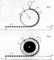
- FIGS. 5 and 6 Shown embodiments are shown structure stamp 1 IV , 1 V , which are contacted by rotational movement about an axis of rotation of the structure stamp 1 with a target surface 4o of a substrate 4 continuously by rolling along the target surface 4o.
- FIG. 1 shows a first embodiment of the invention, preferably made of PFPE, structural stamp 1 with structures 2, at the embossing surface 2o an embossing material 3 adheres.
- the embossing material 3 has a first surface 3o facing the embossing surface 2o and a second side 3u facing a target surface 4o of the substrate 4.
- the embossing material 3 is previously applied to the embossing surface 20 in a coating step, not shown, by immersing the structures 2 in a reservoir of the, in particular liquid, embossing material 3.
- FIG. 2 shows a second embodiment of the invention, preferably made of PFPE, structural stamp 1 ', which differs by its pores 5 from the structure of the temple 1.
- the pores 5 have an open porosity, so that the fluid transport of the embossing material 3 of a to the embossing surface 2o facing away from back 1o of the stamp 1 'to the embossing surface 2o of the structures 2 can be done.
- FIG. 3 shows a third embodiment according to the invention of a, preferably made of PFPE, structural stamp 1 ", which differs from the stamp 1 'by a film 8, which was attached to its rear side 10th
- the film 8 has elevations 10, which separate cavities 9 from each other Cavities 9 serve to receive the embossing material 3, which diffuses through the stamp 1 "and can thus reach the embossing surface 2o of the structures 2.
- the elevations 10 may be in particular columns or pillars or elongated, extending over the entire width walls.
- the elevations 10 serve primarily to support the stamp 1 "
- the film 8 has a thickness of between 100 and 2000 ⁇ m
- the height of the cavities 9 or height of the elevations 10 is between 100 ⁇ m and 500 ⁇ m
- the film 8 is preferably on a side circumference 11 Slide 8 and the structure stamp 1 with the stamp 1 "connected. This may be a bonding, welding or other, preferably unsolvable, connection type.
- FIG. 4 shows a fourth embodiment of a punch 1 "'according to the invention, which is mounted on a carrier 14, which is also preferably porous.
- the carrier 14 is preferably made of a ceramic or a metal or of a high-strength and hard polymer. 'and the carrier 14 are surrounded by a shield 12.
- the embossing material 3 can be stored in a cavity 15 above the carrier 14.
- the diffusion of the molecular component 3 through the support plate 14 and the punch 1 "' is carried out analogously as in the other embodiments mentioned
- the carrier 14 can be connected to the punch 1"' by the material of the punch 1 "'in the porous Structure of the carrier 14 moves or during the manufacturing process of Connection is forced.
- the stamp 1"' can be produced, for example, on the carrier 14.
- the highly viscous but still liquid embossing composition from which the stamp 1 "'is produced may partially penetrate already into the pores of the carrier 14 and thus establish a connection between the two elements '' This is firmly connected to the stamp 14.
- the carrier 14 and the punch 1 ''' not be connected to each other, but can also be pressed against each other only by the shield 12 or any other device or at least held together.
- FIG. 5 shows a fifth embodiment of a structural stamp according to the invention 1 IV in the form of a, preferably made of PFPE roller 1, which can be regarded as a round die.
- a dispenser 6 ensures a, in particular continuous and lasting, wetting of the embossing surface 2o of the structures 2 with the embossing material 3.
- the embossing material 3 is transferred to the target surface 4o.
- the structure stamp 1 IV is rotatably supported about a rotation axis 7, while the substrate 4 is moved at a speed v translationally or tangentially to the roller.
- FIG. 6 shows a sixth embodiment of a structural stamp according to the invention 1 IV in the form of a, preferably made of PFPE roller 1, which can be considered as a round die.
- the structure stamp 1 V is made as a hollow shaft. A cavity in the interior of the hollow shaft serves as a reservoir for the embossing material 3.
- the structure stamp 1 V has a porous porous structure of pores 5, which the passage of the embossing material 3 from the cavity to the surface 2o of the structures 2 allowed.
Landscapes
- Engineering & Computer Science (AREA)
- Physics & Mathematics (AREA)
- Chemical & Material Sciences (AREA)
- Nanotechnology (AREA)
- General Physics & Mathematics (AREA)
- Crystallography & Structural Chemistry (AREA)
- Manufacturing & Machinery (AREA)
- Condensed Matter Physics & Semiconductors (AREA)
- Mathematical Physics (AREA)
- Theoretical Computer Science (AREA)
- Shaping Of Tube Ends By Bending Or Straightening (AREA)
- Spectroscopy & Molecular Physics (AREA)
- Micromachines (AREA)
- Exposure Of Semiconductors, Excluding Electron Or Ion Beam Exposure (AREA)
Claims (6)
- Procédé de matriçage par micro-contact d'une structure par transfert d'un matériau de matriçage (3) sur une surface cible (40) d'un substrat (4) au moyen d'une surface de matriçage (20) d'un poinçon de structure (1), caractérisé en ce que le matériau de matriçage (3) est composé majoritairement de silane ou au moins majoritairement d'au moins un dérivé de silane, ou est une composante moléculaire composée au moins majoritairement de molécules organiques, et que le poinçon de structure (1) est un poinçon souple, sachant que le poinçon de structure (1) est fabriqué sous forme d'un rouleau en tant qu'arbre creux, sachant que l'espace creux à l'intérieur de l'arbre creux sert de réservoir pour le matériau de matriçage (3), sachant que le poinçon de structure (1) possède une microstructure poreuse faite de pores (5) qui permet le passage du matériau de matriçage (3) de l'espace creux à la surface (20) de structures (2).
- Procédé selon la revendication 1, dans lequel la composante moléculaire présente au moins une ou plusieurs des structures listées ci-après :- enzymes- alcaloïdes- lipides- hormones- phéromones- vitamines,- hydrates de carbone- peptides- acides nucléiques- ADN ou chaînes d'ADN,- cellules- protéines, respectivement peptides,- alcanes, alcènes, alkynes, aromates,- graphes.
- Procédé selon l'une des revendications précédentes, dans lequel le poinçon de structure (1) présente une élasticité/un module d'élasticité de 10-3 MPa et 100 MPa, de préférence entre 10-2 MPa et 80 MPa, avec une plus grande préférence entre 10-1 MPa et 60 MPa, de façon la plus préférée entre 3 MPa et 40 MPa.
- Procédé selon l'une des revendications précédentes, dans lequel le poinçon de structure (1) est résistant aux acides et/ou aux bases.
- Procédé selon l'une des revendications précédentes, dans lequel le poinçon de structure (1) est composé majoritairement, de préférence intégralement, d'un matériau inerte.
- Procédé selon l'une des revendications précédentes, dans lequel le poinçon de structure (1) est fabriqué dans un polymère, en particulier en PFPE ou en PDMS.
Applications Claiming Priority (2)
| Application Number | Priority Date | Filing Date | Title |
|---|---|---|---|
| DE102012112030.7A DE102012112030A1 (de) | 2012-12-10 | 2012-12-10 | Verfahren zum Mikrokontaktprägen |
| PCT/EP2013/075562 WO2014090661A1 (fr) | 2012-12-10 | 2013-12-04 | Procédé de poinçonnage de microcontacts |
Publications (2)
| Publication Number | Publication Date |
|---|---|
| EP2888629A1 EP2888629A1 (fr) | 2015-07-01 |
| EP2888629B1 true EP2888629B1 (fr) | 2016-03-02 |
Family
ID=49709685
Family Applications (1)
| Application Number | Title | Priority Date | Filing Date |
|---|---|---|---|
| EP13799316.8A Active EP2888629B1 (fr) | 2012-12-10 | 2013-12-04 | Procédé de poinçonnage de microcontacts |
Country Status (8)
| Country | Link |
|---|---|
| US (1) | US9323144B2 (fr) |
| EP (1) | EP2888629B1 (fr) |
| JP (1) | JP2016511931A (fr) |
| KR (1) | KR101759810B1 (fr) |
| CN (2) | CN110376844A (fr) |
| DE (1) | DE102012112030A1 (fr) |
| SG (1) | SG11201503318PA (fr) |
| WO (1) | WO2014090661A1 (fr) |
Families Citing this family (13)
| Publication number | Priority date | Publication date | Assignee | Title |
|---|---|---|---|---|
| TWI659475B (zh) * | 2014-07-20 | 2019-05-11 | 愛爾蘭商艾克斯瑟樂普林特有限公司 | 用於微轉貼印刷之裝置及方法 |
| EP3215895B1 (fr) * | 2014-11-03 | 2022-02-23 | Universität Osnabrück | Procédé de réalisation d'une nanoimpression capillaire, champ de gouttes d'encre et champ de cables obtenus par ledit procédé |
| CN104356740B (zh) * | 2014-11-05 | 2017-05-17 | 广西师范学院 | 利用水溶性卟啉铁配合物进行微接触印刷的方法 |
| WO2016102185A1 (fr) | 2014-12-22 | 2016-06-30 | Koninklijke Philips N.V. | Procédé de fabrication de tampon à motif, tampon à motif et procédé d'impression |
| WO2016206746A1 (fr) * | 2015-06-25 | 2016-12-29 | Ev Group E. Thallner Gmbh | Procédé de réalisation de structures sur une surface de substrat |
| CN106486209A (zh) * | 2015-08-31 | 2017-03-08 | 中国科学院宁波材料技术与工程研究所 | 一种图案化3d石墨烯导电薄膜及其绿色制备方法和应用 |
| CN105319840A (zh) * | 2015-11-23 | 2016-02-10 | 南通天鸿镭射科技有限公司 | 利用复制技术制作紫外光固化无缝成型辊轮的装置及方法 |
| KR102331438B1 (ko) * | 2016-04-06 | 2021-11-26 | 코닌클리케 필립스 엔.브이. | 임프린트 리소그래피 스탬프, 이의 제조 방법 및 사용 방법 |
| CN106542494B (zh) * | 2016-09-26 | 2017-12-26 | 西北工业大学 | 一种用于制备多层不等高微纳结构的方法 |
| JP6854733B2 (ja) * | 2017-08-17 | 2021-04-07 | 株式会社ジェイエスピー | 樹脂シート |
| CN111747372B (zh) * | 2019-03-26 | 2024-06-14 | 深圳清力技术有限公司 | 一种无边缘凸起的金属盖石墨岛及其制备方法 |
| KR20250153308A (ko) * | 2019-12-02 | 2025-10-24 | 에베 그룹 에. 탈너 게엠베하 | 스탬프를 분리하는 방법 및 장치 |
| US12055737B2 (en) * | 2022-05-18 | 2024-08-06 | GE Precision Healthcare LLC | Aligned and stacked high-aspect ratio metallized structures |
Family Cites Families (23)
| Publication number | Priority date | Publication date | Assignee | Title |
|---|---|---|---|---|
| NL261937A (fr) * | 1960-03-16 | 1900-01-01 | ||
| US3678848A (en) * | 1969-08-25 | 1972-07-25 | Weber Marking Systems Inc | Inking pad and use thereof |
| US3709647A (en) * | 1970-10-21 | 1973-01-09 | Clear Pack Co | Apparatus for forming an embossed thermoplastic sheet |
| JPS5436617B2 (fr) * | 1973-02-07 | 1979-11-10 | ||
| US3971315A (en) * | 1974-08-12 | 1976-07-27 | Porelon, Inc. | Macroporous microporous marking structure |
| JPH10278217A (ja) * | 1997-04-09 | 1998-10-20 | Asahi Optical Co Ltd | 印刷版とその製造方法及びその印刷版を用いた印刷装置 |
| US6276272B1 (en) * | 1996-10-01 | 2001-08-21 | Brother Kogyo Kabushiki Kaisha | Stamp plate producing apparatus for producing stamp plate used in a stamp device |
| US6048623A (en) * | 1996-12-18 | 2000-04-11 | Kimberly-Clark Worldwide, Inc. | Method of contact printing on gold coated films |
| DE19949993C1 (de) * | 1999-10-15 | 2001-05-03 | Peter Barth | Verfahren zur Oberflächenstrukturierung |
| DE60118843T2 (de) * | 2000-02-07 | 2006-11-30 | Koninklijke Philips Electronics N.V. | Stempel für ein lithographisches verfahren, methode zur stempelherstellung und methode zur herstellung einer gemusterten schicht auf einem substrat |
| CN1299165C (zh) * | 2000-11-22 | 2007-02-07 | 皇家菲利浦电子有限公司 | 印模,方法和设备 |
| US6817293B2 (en) | 2001-03-28 | 2004-11-16 | Dainippon Printing Co., Ltd. | Patterning method with micro-contact printing and its printed product |
| JP5055672B2 (ja) * | 2001-07-31 | 2012-10-24 | 大日本印刷株式会社 | 薄膜パターン形成用スタンプ |
| US20030127002A1 (en) | 2002-01-04 | 2003-07-10 | Hougham Gareth Geoffrey | Multilayer architechture for microcontact printing stamps |
| GB0326904D0 (en) * | 2003-11-19 | 2003-12-24 | Koninkl Philips Electronics Nv | Formation of self-assembled monolayers |
| WO2006043244A1 (fr) * | 2004-10-22 | 2006-04-27 | Koninklijke Philips Electronics N.V. | Systeme d'impression par micro-contact au rouleau avec regulation de la pression |
| ATE544093T1 (de) * | 2006-11-01 | 2012-02-15 | Koninkl Philips Electronics Nv | Imprintmethode zur herstellung einer reliefschicht und deren nutzung als ätzmaske |
| US20080230773A1 (en) | 2007-03-20 | 2008-09-25 | Nano Terra Inc. | Polymer Composition for Preparing Electronic Devices by Microcontact Printing Processes and Products Prepared by the Processes |
| US7959975B2 (en) | 2007-04-18 | 2011-06-14 | Micron Technology, Inc. | Methods of patterning a substrate |
| US9003970B2 (en) * | 2008-06-30 | 2015-04-14 | 3M Innovative Properties Company | Solvent assisted method of microcontact printing |
| JP2010171281A (ja) * | 2009-01-23 | 2010-08-05 | Jsr Corp | インプリント方法 |
| US20100252955A1 (en) * | 2009-04-01 | 2010-10-07 | Nano Terra Inc. | Methods of Patterning Substrates Using Microcontact Printed Polymer Resists and Articles Prepared Therefrom |
| JP5843784B2 (ja) * | 2009-12-22 | 2016-01-13 | スリーエム イノベイティブ プロパティズ カンパニー | 加圧ローラーを使用するマイクロコンタクトプリンティングのための装置及び方法 |
-
2012
- 2012-12-10 DE DE102012112030.7A patent/DE102012112030A1/de not_active Ceased
-
2013
- 2013-12-04 JP JP2015546946A patent/JP2016511931A/ja active Pending
- 2013-12-04 KR KR1020157014532A patent/KR101759810B1/ko active Active
- 2013-12-04 CN CN201910665524.5A patent/CN110376844A/zh active Pending
- 2013-12-04 CN CN201380064460.4A patent/CN104823107A/zh active Pending
- 2013-12-04 WO PCT/EP2013/075562 patent/WO2014090661A1/fr not_active Ceased
- 2013-12-04 US US14/439,860 patent/US9323144B2/en active Active
- 2013-12-04 EP EP13799316.8A patent/EP2888629B1/fr active Active
- 2013-12-04 SG SG11201503318PA patent/SG11201503318PA/en unknown
Also Published As
| Publication number | Publication date |
|---|---|
| KR101759810B1 (ko) | 2017-07-19 |
| DE102012112030A1 (de) | 2014-06-12 |
| SG11201503318PA (en) | 2015-06-29 |
| KR20150092139A (ko) | 2015-08-12 |
| EP2888629A1 (fr) | 2015-07-01 |
| WO2014090661A1 (fr) | 2014-06-19 |
| JP2016511931A (ja) | 2016-04-21 |
| CN110376844A (zh) | 2019-10-25 |
| CN104823107A (zh) | 2015-08-05 |
| US9323144B2 (en) | 2016-04-26 |
| US20150293442A1 (en) | 2015-10-15 |
Similar Documents
| Publication | Publication Date | Title |
|---|---|---|
| EP2888629B1 (fr) | Procédé de poinçonnage de microcontacts | |
| DE60029445T2 (de) | Verfahren zur strukturierung von polymerschichten, und anwendung der verfahren | |
| DE60310443T2 (de) | Druckverfahren mit gummistempel | |
| EP2150854B1 (fr) | Poinçon pour impression par microcontact et son procede de fabrication | |
| EP3215895B1 (fr) | Procédé de réalisation d'une nanoimpression capillaire, champ de gouttes d'encre et champ de cables obtenus par ledit procédé | |
| EP2870510B1 (fr) | Poinçon structuré, dispositif et procédé pour l'estampage | |
| EP2329319B1 (fr) | Procédé amélioré de nano-impression | |
| DE102013216540A1 (de) | Transfervorrichtung und ausgeformtes Material | |
| EP3011391B1 (fr) | Matrice pourvue d'une structure et procédé pour la fabriquer | |
| DE19935558B4 (de) | Verfahren zur Erzeugung von Strukturen in einem Substrat im Nanometerbereich | |
| DE102004033440A1 (de) | Mikrostrukturierte Vorrichtung und Verfahren zu ihrer Herstellung | |
| WO2022175361A1 (fr) | Système microfluidique constitué d'une feuille pliée, et procédé de production | |
| DE102008055960A1 (de) | Felder von Nanosticheln für Feinstdruck- und Prägeverfahren | |
| EP3555705B1 (fr) | Dispositif et procédé de réalisation de nanostructures périodiques de grande surface sur un substrat planaire au moyen d'un procédé de nano-impression | |
| Choonee et al. | Multilevel self-aligned microcontact printing system | |
| DE10207393A1 (de) | Rapid Prototyping durch Drucken von organischen Substanzen und deren Verfestigung | |
| EP4176311B1 (fr) | Procédé de production de microstructures et/ou de nanostructures | |
| EP2771161B1 (fr) | Structure de formage nanométrique | |
| Kim et al. | In situ curing of sliding SU-8 droplet over a microcontact printed pattern for tunable fabrication of a polydimethylsiloxane nanoslit | |
| EP4735956A1 (fr) | Procédé d'utilisation d'un tampon dur pour produire un tampon souple | |
| DE102018117873A1 (de) | Mikrofluide Einheit und ein Verfahren zu deren Herstellung | |
| DE102009018849A1 (de) | Masterstruktur zum Prägen und/oder Bedrucken eines Grundmaterials, Vorrichtung zum kontinuierlichen Prägen und/oder Bedrucken eines Grundmaterials und Verfahren zum Herstellen einer Masterstruktur zum Prägen und/oder Bedrucken eines Grundmaterials | |
| DE102012023514B3 (de) | Vorrichtung zum Übertragen einer Zellsuspension, entsprechendes System und entsprechendes Verfahren | |
| WO2008154907A2 (fr) | Procédé et dispositif de transfert de micro- ou de nanostructures par poinçons de contact | |
| DE102017011726A1 (de) | Lamination von Polymerschichten |
Legal Events
| Date | Code | Title | Description |
|---|---|---|---|
| PUAI | Public reference made under article 153(3) epc to a published international application that has entered the european phase |
Free format text: ORIGINAL CODE: 0009012 |
|
| 17P | Request for examination filed |
Effective date: 20150325 |
|
| AK | Designated contracting states |
Kind code of ref document: A1 Designated state(s): AL AT BE BG CH CY CZ DE DK EE ES FI FR GB GR HR HU IE IS IT LI LT LU LV MC MK MT NL NO PL PT RO RS SE SI SK SM TR |
|
| AX | Request for extension of the european patent |
Extension state: BA ME |
|
| GRAP | Despatch of communication of intention to grant a patent |
Free format text: ORIGINAL CODE: EPIDOSNIGR1 |
|
| GRAJ | Information related to disapproval of communication of intention to grant by the applicant or resumption of examination proceedings by the epo deleted |
Free format text: ORIGINAL CODE: EPIDOSDIGR1 |
|
| GRAP | Despatch of communication of intention to grant a patent |
Free format text: ORIGINAL CODE: EPIDOSNIGR1 |
|
| DAX | Request for extension of the european patent (deleted) | ||
| INTG | Intention to grant announced |
Effective date: 20150918 |
|
| INTG | Intention to grant announced |
Effective date: 20151005 |
|
| GRAS | Grant fee paid |
Free format text: ORIGINAL CODE: EPIDOSNIGR3 |
|
| GRAA | (expected) grant |
Free format text: ORIGINAL CODE: 0009210 |
|
| AK | Designated contracting states |
Kind code of ref document: B1 Designated state(s): AL AT BE BG CH CY CZ DE DK EE ES FI FR GB GR HR HU IE IS IT LI LT LU LV MC MK MT NL NO PL PT RO RS SE SI SK SM TR |
|
| REG | Reference to a national code |
Ref country code: GB Ref legal event code: FG4D Free format text: NOT ENGLISH |
|
| REG | Reference to a national code |
Ref country code: AT Ref legal event code: REF Ref document number: 778435 Country of ref document: AT Kind code of ref document: T Effective date: 20160315 Ref country code: CH Ref legal event code: EP |
|
| REG | Reference to a national code |
Ref country code: IE Ref legal event code: FG4D Free format text: LANGUAGE OF EP DOCUMENT: GERMAN |
|
| REG | Reference to a national code |
Ref country code: DE Ref legal event code: R096 Ref document number: 502013002079 Country of ref document: DE |
|
| REG | Reference to a national code |
Ref country code: NL Ref legal event code: MP Effective date: 20160302 |
|
| REG | Reference to a national code |
Ref country code: LT Ref legal event code: MG4D |
|
| PG25 | Lapsed in a contracting state [announced via postgrant information from national office to epo] |
Ref country code: FI Free format text: LAPSE BECAUSE OF FAILURE TO SUBMIT A TRANSLATION OF THE DESCRIPTION OR TO PAY THE FEE WITHIN THE PRESCRIBED TIME-LIMIT Effective date: 20160302 Ref country code: ES Free format text: LAPSE BECAUSE OF FAILURE TO SUBMIT A TRANSLATION OF THE DESCRIPTION OR TO PAY THE FEE WITHIN THE PRESCRIBED TIME-LIMIT Effective date: 20160302 Ref country code: GR Free format text: LAPSE BECAUSE OF FAILURE TO SUBMIT A TRANSLATION OF THE DESCRIPTION OR TO PAY THE FEE WITHIN THE PRESCRIBED TIME-LIMIT Effective date: 20160603 Ref country code: NO Free format text: LAPSE BECAUSE OF FAILURE TO SUBMIT A TRANSLATION OF THE DESCRIPTION OR TO PAY THE FEE WITHIN THE PRESCRIBED TIME-LIMIT Effective date: 20160602 Ref country code: HR Free format text: LAPSE BECAUSE OF FAILURE TO SUBMIT A TRANSLATION OF THE DESCRIPTION OR TO PAY THE FEE WITHIN THE PRESCRIBED TIME-LIMIT Effective date: 20160302 |
|
| PG25 | Lapsed in a contracting state [announced via postgrant information from national office to epo] |
Ref country code: LV Free format text: LAPSE BECAUSE OF FAILURE TO SUBMIT A TRANSLATION OF THE DESCRIPTION OR TO PAY THE FEE WITHIN THE PRESCRIBED TIME-LIMIT Effective date: 20160302 Ref country code: SE Free format text: LAPSE BECAUSE OF FAILURE TO SUBMIT A TRANSLATION OF THE DESCRIPTION OR TO PAY THE FEE WITHIN THE PRESCRIBED TIME-LIMIT Effective date: 20160302 Ref country code: PL Free format text: LAPSE BECAUSE OF FAILURE TO SUBMIT A TRANSLATION OF THE DESCRIPTION OR TO PAY THE FEE WITHIN THE PRESCRIBED TIME-LIMIT Effective date: 20160302 Ref country code: NL Free format text: LAPSE BECAUSE OF FAILURE TO SUBMIT A TRANSLATION OF THE DESCRIPTION OR TO PAY THE FEE WITHIN THE PRESCRIBED TIME-LIMIT Effective date: 20160302 Ref country code: LT Free format text: LAPSE BECAUSE OF FAILURE TO SUBMIT A TRANSLATION OF THE DESCRIPTION OR TO PAY THE FEE WITHIN THE PRESCRIBED TIME-LIMIT Effective date: 20160302 Ref country code: RS Free format text: LAPSE BECAUSE OF FAILURE TO SUBMIT A TRANSLATION OF THE DESCRIPTION OR TO PAY THE FEE WITHIN THE PRESCRIBED TIME-LIMIT Effective date: 20160302 |
|
| PG25 | Lapsed in a contracting state [announced via postgrant information from national office to epo] |
Ref country code: EE Free format text: LAPSE BECAUSE OF FAILURE TO SUBMIT A TRANSLATION OF THE DESCRIPTION OR TO PAY THE FEE WITHIN THE PRESCRIBED TIME-LIMIT Effective date: 20160302 Ref country code: IS Free format text: LAPSE BECAUSE OF FAILURE TO SUBMIT A TRANSLATION OF THE DESCRIPTION OR TO PAY THE FEE WITHIN THE PRESCRIBED TIME-LIMIT Effective date: 20160702 |
|
| PG25 | Lapsed in a contracting state [announced via postgrant information from national office to epo] |
Ref country code: SM Free format text: LAPSE BECAUSE OF FAILURE TO SUBMIT A TRANSLATION OF THE DESCRIPTION OR TO PAY THE FEE WITHIN THE PRESCRIBED TIME-LIMIT Effective date: 20160302 Ref country code: PT Free format text: LAPSE BECAUSE OF FAILURE TO SUBMIT A TRANSLATION OF THE DESCRIPTION OR TO PAY THE FEE WITHIN THE PRESCRIBED TIME-LIMIT Effective date: 20160704 Ref country code: CZ Free format text: LAPSE BECAUSE OF FAILURE TO SUBMIT A TRANSLATION OF THE DESCRIPTION OR TO PAY THE FEE WITHIN THE PRESCRIBED TIME-LIMIT Effective date: 20160302 Ref country code: SK Free format text: LAPSE BECAUSE OF FAILURE TO SUBMIT A TRANSLATION OF THE DESCRIPTION OR TO PAY THE FEE WITHIN THE PRESCRIBED TIME-LIMIT Effective date: 20160302 Ref country code: RO Free format text: LAPSE BECAUSE OF FAILURE TO SUBMIT A TRANSLATION OF THE DESCRIPTION OR TO PAY THE FEE WITHIN THE PRESCRIBED TIME-LIMIT Effective date: 20160302 |
|
| REG | Reference to a national code |
Ref country code: DE Ref legal event code: R097 Ref document number: 502013002079 Country of ref document: DE |
|
| PG25 | Lapsed in a contracting state [announced via postgrant information from national office to epo] |
Ref country code: IT Free format text: LAPSE BECAUSE OF FAILURE TO SUBMIT A TRANSLATION OF THE DESCRIPTION OR TO PAY THE FEE WITHIN THE PRESCRIBED TIME-LIMIT Effective date: 20160302 |
|
| PLBE | No opposition filed within time limit |
Free format text: ORIGINAL CODE: 0009261 |
|
| STAA | Information on the status of an ep patent application or granted ep patent |
Free format text: STATUS: NO OPPOSITION FILED WITHIN TIME LIMIT |
|
| PG25 | Lapsed in a contracting state [announced via postgrant information from national office to epo] |
Ref country code: DK Free format text: LAPSE BECAUSE OF FAILURE TO SUBMIT A TRANSLATION OF THE DESCRIPTION OR TO PAY THE FEE WITHIN THE PRESCRIBED TIME-LIMIT Effective date: 20160302 |
|
| 26N | No opposition filed |
Effective date: 20161205 |
|
| PG25 | Lapsed in a contracting state [announced via postgrant information from national office to epo] |
Ref country code: BG Free format text: LAPSE BECAUSE OF FAILURE TO SUBMIT A TRANSLATION OF THE DESCRIPTION OR TO PAY THE FEE WITHIN THE PRESCRIBED TIME-LIMIT Effective date: 20160602 Ref country code: SI Free format text: LAPSE BECAUSE OF FAILURE TO SUBMIT A TRANSLATION OF THE DESCRIPTION OR TO PAY THE FEE WITHIN THE PRESCRIBED TIME-LIMIT Effective date: 20160302 |
|
| PG25 | Lapsed in a contracting state [announced via postgrant information from national office to epo] |
Ref country code: BE Free format text: LAPSE BECAUSE OF NON-PAYMENT OF DUE FEES Effective date: 20161231 |
|
| REG | Reference to a national code |
Ref country code: CH Ref legal event code: PL |
|
| PG25 | Lapsed in a contracting state [announced via postgrant information from national office to epo] |
Ref country code: MC Free format text: LAPSE BECAUSE OF FAILURE TO SUBMIT A TRANSLATION OF THE DESCRIPTION OR TO PAY THE FEE WITHIN THE PRESCRIBED TIME-LIMIT Effective date: 20160302 |
|
| REG | Reference to a national code |
Ref country code: FR Ref legal event code: ST Effective date: 20170831 |
|
| REG | Reference to a national code |
Ref country code: IE Ref legal event code: MM4A |
|
| PG25 | Lapsed in a contracting state [announced via postgrant information from national office to epo] |
Ref country code: CH Free format text: LAPSE BECAUSE OF NON-PAYMENT OF DUE FEES Effective date: 20161231 Ref country code: LU Free format text: LAPSE BECAUSE OF NON-PAYMENT OF DUE FEES Effective date: 20161204 Ref country code: LI Free format text: LAPSE BECAUSE OF NON-PAYMENT OF DUE FEES Effective date: 20161231 Ref country code: FR Free format text: LAPSE BECAUSE OF NON-PAYMENT OF DUE FEES Effective date: 20170102 |
|
| PG25 | Lapsed in a contracting state [announced via postgrant information from national office to epo] |
Ref country code: IE Free format text: LAPSE BECAUSE OF NON-PAYMENT OF DUE FEES Effective date: 20161204 |
|
| REG | Reference to a national code |
Ref country code: BE Ref legal event code: MM Effective date: 20161231 |
|
| PG25 | Lapsed in a contracting state [announced via postgrant information from national office to epo] |
Ref country code: HU Free format text: LAPSE BECAUSE OF FAILURE TO SUBMIT A TRANSLATION OF THE DESCRIPTION OR TO PAY THE FEE WITHIN THE PRESCRIBED TIME-LIMIT; INVALID AB INITIO Effective date: 20131204 |
|
| PG25 | Lapsed in a contracting state [announced via postgrant information from national office to epo] |
Ref country code: MK Free format text: LAPSE BECAUSE OF FAILURE TO SUBMIT A TRANSLATION OF THE DESCRIPTION OR TO PAY THE FEE WITHIN THE PRESCRIBED TIME-LIMIT Effective date: 20160302 Ref country code: CY Free format text: LAPSE BECAUSE OF FAILURE TO SUBMIT A TRANSLATION OF THE DESCRIPTION OR TO PAY THE FEE WITHIN THE PRESCRIBED TIME-LIMIT Effective date: 20160302 |
|
| GBPC | Gb: european patent ceased through non-payment of renewal fee |
Effective date: 20171204 |
|
| PG25 | Lapsed in a contracting state [announced via postgrant information from national office to epo] |
Ref country code: MT Free format text: LAPSE BECAUSE OF FAILURE TO SUBMIT A TRANSLATION OF THE DESCRIPTION OR TO PAY THE FEE WITHIN THE PRESCRIBED TIME-LIMIT Effective date: 20160302 |
|
| PG25 | Lapsed in a contracting state [announced via postgrant information from national office to epo] |
Ref country code: AL Free format text: LAPSE BECAUSE OF FAILURE TO SUBMIT A TRANSLATION OF THE DESCRIPTION OR TO PAY THE FEE WITHIN THE PRESCRIBED TIME-LIMIT Effective date: 20160302 Ref country code: TR Free format text: LAPSE BECAUSE OF FAILURE TO SUBMIT A TRANSLATION OF THE DESCRIPTION OR TO PAY THE FEE WITHIN THE PRESCRIBED TIME-LIMIT Effective date: 20160302 |
|
| PG25 | Lapsed in a contracting state [announced via postgrant information from national office to epo] |
Ref country code: GB Free format text: LAPSE BECAUSE OF NON-PAYMENT OF DUE FEES Effective date: 20171204 |
|
| PGFP | Annual fee paid to national office [announced via postgrant information from national office to epo] |
Ref country code: AT Payment date: 20251215 Year of fee payment: 13 |
|
| PGFP | Annual fee paid to national office [announced via postgrant information from national office to epo] |
Ref country code: DE Payment date: 20251222 Year of fee payment: 13 |