EP2899863A1 - Alimentation électrique - Google Patents
Alimentation électrique Download PDFInfo
- Publication number
- EP2899863A1 EP2899863A1 EP14275255.9A EP14275255A EP2899863A1 EP 2899863 A1 EP2899863 A1 EP 2899863A1 EP 14275255 A EP14275255 A EP 14275255A EP 2899863 A1 EP2899863 A1 EP 2899863A1
- Authority
- EP
- European Patent Office
- Prior art keywords
- power
- voltage level
- driving power
- power supply
- unit
- Prior art date
- Legal status (The legal status is an assumption and is not a legal conclusion. Google has not performed a legal analysis and makes no representation as to the accuracy of the status listed.)
- Withdrawn
Links
- 230000008859 change Effects 0.000 claims abstract description 14
- 238000001514 detection method Methods 0.000 claims description 39
- 230000001131 transforming effect Effects 0.000 claims description 10
- 208000032365 Electromagnetic interference Diseases 0.000 claims description 3
- 238000001914 filtration Methods 0.000 claims description 2
- 238000010586 diagram Methods 0.000 description 12
- 230000006870 function Effects 0.000 description 11
- 238000000034 method Methods 0.000 description 8
- 230000008569 process Effects 0.000 description 7
- 238000004804 winding Methods 0.000 description 7
- 230000014509 gene expression Effects 0.000 description 3
- 230000008901 benefit Effects 0.000 description 2
- XUIMIQQOPSSXEZ-UHFFFAOYSA-N Silicon Chemical compound [Si] XUIMIQQOPSSXEZ-UHFFFAOYSA-N 0.000 description 1
- 239000003990 capacitor Substances 0.000 description 1
- 238000006243 chemical reaction Methods 0.000 description 1
- 230000001276 controlling effect Effects 0.000 description 1
- 230000000694 effects Effects 0.000 description 1
- 230000005669 field effect Effects 0.000 description 1
- 238000009499 grossing Methods 0.000 description 1
- 229910044991 metal oxide Inorganic materials 0.000 description 1
- 150000004706 metal oxides Chemical class 0.000 description 1
- 230000004048 modification Effects 0.000 description 1
- 238000012986 modification Methods 0.000 description 1
- 230000009467 reduction Effects 0.000 description 1
- 230000001105 regulatory effect Effects 0.000 description 1
- 230000004044 response Effects 0.000 description 1
- 229910052710 silicon Inorganic materials 0.000 description 1
- 239000010703 silicon Substances 0.000 description 1
- 235000015096 spirit Nutrition 0.000 description 1
- 239000003381 stabilizer Substances 0.000 description 1
Images


Classifications
-
- H—ELECTRICITY
- H05—ELECTRIC TECHNIQUES NOT OTHERWISE PROVIDED FOR
- H05B—ELECTRIC HEATING; ELECTRIC LIGHT SOURCES NOT OTHERWISE PROVIDED FOR; CIRCUIT ARRANGEMENTS FOR ELECTRIC LIGHT SOURCES, IN GENERAL
- H05B45/00—Circuit arrangements for operating light-emitting diodes [LED]
- H05B45/30—Driver circuits
- H05B45/37—Converter circuits
- H05B45/3725—Switched mode power supply [SMPS]
- H05B45/385—Switched mode power supply [SMPS] using flyback topology
-
- H—ELECTRICITY
- H02—GENERATION; CONVERSION OR DISTRIBUTION OF ELECTRIC POWER
- H02M—APPARATUS FOR CONVERSION BETWEEN AC AND AC, BETWEEN AC AND DC, OR BETWEEN DC AND DC, AND FOR USE WITH MAINS OR SIMILAR POWER SUPPLY SYSTEMS; CONVERSION OF DC OR AC INPUT POWER INTO SURGE OUTPUT POWER; CONTROL OR REGULATION THEREOF
- H02M1/00—Details of apparatus for conversion
- H02M1/12—Arrangements for reducing harmonics from AC input or output
- H02M1/126—Arrangements for reducing harmonics from AC input or output using passive filters
-
- H—ELECTRICITY
- H02—GENERATION; CONVERSION OR DISTRIBUTION OF ELECTRIC POWER
- H02M—APPARATUS FOR CONVERSION BETWEEN AC AND AC, BETWEEN AC AND DC, OR BETWEEN DC AND DC, AND FOR USE WITH MAINS OR SIMILAR POWER SUPPLY SYSTEMS; CONVERSION OF DC OR AC INPUT POWER INTO SURGE OUTPUT POWER; CONTROL OR REGULATION THEREOF
- H02M1/00—Details of apparatus for conversion
- H02M1/42—Circuits or arrangements for compensating for or adjusting power factor in converters or inverters
- H02M1/4208—Arrangements for improving power factor of AC input
- H02M1/4225—Arrangements for improving power factor of AC input using a non-isolated boost converter
-
- H—ELECTRICITY
- H02—GENERATION; CONVERSION OR DISTRIBUTION OF ELECTRIC POWER
- H02M—APPARATUS FOR CONVERSION BETWEEN AC AND AC, BETWEEN AC AND DC, OR BETWEEN DC AND DC, AND FOR USE WITH MAINS OR SIMILAR POWER SUPPLY SYSTEMS; CONVERSION OF DC OR AC INPUT POWER INTO SURGE OUTPUT POWER; CONTROL OR REGULATION THEREOF
- H02M3/00—Conversion of DC power input into DC power output
- H02M3/22—Conversion of DC power input into DC power output with intermediate conversion into AC
- H02M3/24—Conversion of DC power input into DC power output with intermediate conversion into AC by static converters
- H02M3/28—Conversion of DC power input into DC power output with intermediate conversion into AC by static converters using discharge tubes with control electrode or semiconductor devices with control electrode to produce the intermediate AC
- H02M3/325—Conversion of DC power input into DC power output with intermediate conversion into AC by static converters using discharge tubes with control electrode or semiconductor devices with control electrode to produce the intermediate AC using devices of a triode or a transistor type requiring continuous application of a control signal
- H02M3/335—Conversion of DC power input into DC power output with intermediate conversion into AC by static converters using discharge tubes with control electrode or semiconductor devices with control electrode to produce the intermediate AC using devices of a triode or a transistor type requiring continuous application of a control signal using semiconductor devices only
- H02M3/33507—Conversion of DC power input into DC power output with intermediate conversion into AC by static converters using discharge tubes with control electrode or semiconductor devices with control electrode to produce the intermediate AC using devices of a triode or a transistor type requiring continuous application of a control signal using semiconductor devices only with automatic control of the output voltage or current, e.g. flyback converters
-
- H—ELECTRICITY
- H02—GENERATION; CONVERSION OR DISTRIBUTION OF ELECTRIC POWER
- H02M—APPARATUS FOR CONVERSION BETWEEN AC AND AC, BETWEEN AC AND DC, OR BETWEEN DC AND DC, AND FOR USE WITH MAINS OR SIMILAR POWER SUPPLY SYSTEMS; CONVERSION OF DC OR AC INPUT POWER INTO SURGE OUTPUT POWER; CONTROL OR REGULATION THEREOF
- H02M3/00—Conversion of DC power input into DC power output
- H02M3/22—Conversion of DC power input into DC power output with intermediate conversion into AC
- H02M3/24—Conversion of DC power input into DC power output with intermediate conversion into AC by static converters
- H02M3/28—Conversion of DC power input into DC power output with intermediate conversion into AC by static converters using discharge tubes with control electrode or semiconductor devices with control electrode to produce the intermediate AC
- H02M3/325—Conversion of DC power input into DC power output with intermediate conversion into AC by static converters using discharge tubes with control electrode or semiconductor devices with control electrode to produce the intermediate AC using devices of a triode or a transistor type requiring continuous application of a control signal
- H02M3/335—Conversion of DC power input into DC power output with intermediate conversion into AC by static converters using discharge tubes with control electrode or semiconductor devices with control electrode to produce the intermediate AC using devices of a triode or a transistor type requiring continuous application of a control signal using semiconductor devices only
- H02M3/33507—Conversion of DC power input into DC power output with intermediate conversion into AC by static converters using discharge tubes with control electrode or semiconductor devices with control electrode to produce the intermediate AC using devices of a triode or a transistor type requiring continuous application of a control signal using semiconductor devices only with automatic control of the output voltage or current, e.g. flyback converters
- H02M3/33515—Conversion of DC power input into DC power output with intermediate conversion into AC by static converters using discharge tubes with control electrode or semiconductor devices with control electrode to produce the intermediate AC using devices of a triode or a transistor type requiring continuous application of a control signal using semiconductor devices only with automatic control of the output voltage or current, e.g. flyback converters with digital control
-
- H—ELECTRICITY
- H02—GENERATION; CONVERSION OR DISTRIBUTION OF ELECTRIC POWER
- H02M—APPARATUS FOR CONVERSION BETWEEN AC AND AC, BETWEEN AC AND DC, OR BETWEEN DC AND DC, AND FOR USE WITH MAINS OR SIMILAR POWER SUPPLY SYSTEMS; CONVERSION OF DC OR AC INPUT POWER INTO SURGE OUTPUT POWER; CONTROL OR REGULATION THEREOF
- H02M3/00—Conversion of DC power input into DC power output
- H02M3/22—Conversion of DC power input into DC power output with intermediate conversion into AC
- H02M3/24—Conversion of DC power input into DC power output with intermediate conversion into AC by static converters
- H02M3/28—Conversion of DC power input into DC power output with intermediate conversion into AC by static converters using discharge tubes with control electrode or semiconductor devices with control electrode to produce the intermediate AC
- H02M3/325—Conversion of DC power input into DC power output with intermediate conversion into AC by static converters using discharge tubes with control electrode or semiconductor devices with control electrode to produce the intermediate AC using devices of a triode or a transistor type requiring continuous application of a control signal
- H02M3/335—Conversion of DC power input into DC power output with intermediate conversion into AC by static converters using discharge tubes with control electrode or semiconductor devices with control electrode to produce the intermediate AC using devices of a triode or a transistor type requiring continuous application of a control signal using semiconductor devices only
- H02M3/33507—Conversion of DC power input into DC power output with intermediate conversion into AC by static converters using discharge tubes with control electrode or semiconductor devices with control electrode to produce the intermediate AC using devices of a triode or a transistor type requiring continuous application of a control signal using semiconductor devices only with automatic control of the output voltage or current, e.g. flyback converters
- H02M3/33523—Conversion of DC power input into DC power output with intermediate conversion into AC by static converters using discharge tubes with control electrode or semiconductor devices with control electrode to produce the intermediate AC using devices of a triode or a transistor type requiring continuous application of a control signal using semiconductor devices only with automatic control of the output voltage or current, e.g. flyback converters with galvanic isolation between input and output of both the power stage and the feedback loop
-
- H—ELECTRICITY
- H02—GENERATION; CONVERSION OR DISTRIBUTION OF ELECTRIC POWER
- H02M—APPARATUS FOR CONVERSION BETWEEN AC AND AC, BETWEEN AC AND DC, OR BETWEEN DC AND DC, AND FOR USE WITH MAINS OR SIMILAR POWER SUPPLY SYSTEMS; CONVERSION OF DC OR AC INPUT POWER INTO SURGE OUTPUT POWER; CONTROL OR REGULATION THEREOF
- H02M7/00—Conversion of AC power input into DC power output; Conversion of DC power input into AC power output
- H02M7/02—Conversion of AC power input into DC power output without possibility of reversal
- H02M7/04—Conversion of AC power input into DC power output without possibility of reversal by static converters
- H02M7/06—Conversion of AC power input into DC power output without possibility of reversal by static converters using discharge tubes without control electrode or semiconductor devices without control electrode
- H02M7/068—Conversion of AC power input into DC power output without possibility of reversal by static converters using discharge tubes without control electrode or semiconductor devices without control electrode mounted on a transformer
-
- H—ELECTRICITY
- H02—GENERATION; CONVERSION OR DISTRIBUTION OF ELECTRIC POWER
- H02M—APPARATUS FOR CONVERSION BETWEEN AC AND AC, BETWEEN AC AND DC, OR BETWEEN DC AND DC, AND FOR USE WITH MAINS OR SIMILAR POWER SUPPLY SYSTEMS; CONVERSION OF DC OR AC INPUT POWER INTO SURGE OUTPUT POWER; CONTROL OR REGULATION THEREOF
- H02M7/00—Conversion of AC power input into DC power output; Conversion of DC power input into AC power output
- H02M7/02—Conversion of AC power input into DC power output without possibility of reversal
- H02M7/04—Conversion of AC power input into DC power output without possibility of reversal by static converters
- H02M7/12—Conversion of AC power input into DC power output without possibility of reversal by static converters using discharge tubes with control electrode or semiconductor devices with control electrode
- H02M7/21—Conversion of AC power input into DC power output without possibility of reversal by static converters using discharge tubes with control electrode or semiconductor devices with control electrode using devices of a triode or transistor type requiring continuous application of a control signal
- H02M7/217—Conversion of AC power input into DC power output without possibility of reversal by static converters using discharge tubes with control electrode or semiconductor devices with control electrode using devices of a triode or transistor type requiring continuous application of a control signal using semiconductor devices only
-
- H—ELECTRICITY
- H05—ELECTRIC TECHNIQUES NOT OTHERWISE PROVIDED FOR
- H05B—ELECTRIC HEATING; ELECTRIC LIGHT SOURCES NOT OTHERWISE PROVIDED FOR; CIRCUIT ARRANGEMENTS FOR ELECTRIC LIGHT SOURCES, IN GENERAL
- H05B45/00—Circuit arrangements for operating light-emitting diodes [LED]
-
- H—ELECTRICITY
- H02—GENERATION; CONVERSION OR DISTRIBUTION OF ELECTRIC POWER
- H02M—APPARATUS FOR CONVERSION BETWEEN AC AND AC, BETWEEN AC AND DC, OR BETWEEN DC AND DC, AND FOR USE WITH MAINS OR SIMILAR POWER SUPPLY SYSTEMS; CONVERSION OF DC OR AC INPUT POWER INTO SURGE OUTPUT POWER; CONTROL OR REGULATION THEREOF
- H02M1/00—Details of apparatus for conversion
- H02M1/0003—Details of control, feedback or regulation circuits
- H02M1/0032—Control circuits allowing low power mode operation, e.g. in standby mode
- H02M1/0035—Control circuits allowing low power mode operation, e.g. in standby mode using burst mode control
-
- H—ELECTRICITY
- H02—GENERATION; CONVERSION OR DISTRIBUTION OF ELECTRIC POWER
- H02M—APPARATUS FOR CONVERSION BETWEEN AC AND AC, BETWEEN AC AND DC, OR BETWEEN DC AND DC, AND FOR USE WITH MAINS OR SIMILAR POWER SUPPLY SYSTEMS; CONVERSION OF DC OR AC INPUT POWER INTO SURGE OUTPUT POWER; CONTROL OR REGULATION THEREOF
- H02M1/00—Details of apparatus for conversion
- H02M1/0048—Circuits or arrangements for reducing losses
- H02M1/0054—Transistor switching losses
- H02M1/0058—Transistor switching losses by employing soft switching techniques, i.e. commutation of transistors when applied voltage is zero or when current flow is zero
-
- H—ELECTRICITY
- H02—GENERATION; CONVERSION OR DISTRIBUTION OF ELECTRIC POWER
- H02M—APPARATUS FOR CONVERSION BETWEEN AC AND AC, BETWEEN AC AND DC, OR BETWEEN DC AND DC, AND FOR USE WITH MAINS OR SIMILAR POWER SUPPLY SYSTEMS; CONVERSION OF DC OR AC INPUT POWER INTO SURGE OUTPUT POWER; CONTROL OR REGULATION THEREOF
- H02M1/00—Details of apparatus for conversion
- H02M1/0067—Converter structures employing plural converter units, other than for parallel operation of the units on a single load
- H02M1/007—Plural converter units in cascade
-
- Y—GENERAL TAGGING OF NEW TECHNOLOGICAL DEVELOPMENTS; GENERAL TAGGING OF CROSS-SECTIONAL TECHNOLOGIES SPANNING OVER SEVERAL SECTIONS OF THE IPC; TECHNICAL SUBJECTS COVERED BY FORMER USPC CROSS-REFERENCE ART COLLECTIONS [XRACs] AND DIGESTS
- Y02—TECHNOLOGIES OR APPLICATIONS FOR MITIGATION OR ADAPTATION AGAINST CLIMATE CHANGE
- Y02B—CLIMATE CHANGE MITIGATION TECHNOLOGIES RELATED TO BUILDINGS, e.g. HOUSING, HOUSE APPLIANCES OR RELATED END-USER APPLICATIONS
- Y02B70/00—Technologies for an efficient end-user side electric power management and consumption
- Y02B70/10—Technologies improving the efficiency by using switched-mode power supplies [SMPS], i.e. efficient power electronics conversion e.g. power factor correction or reduction of losses in power supplies or efficient standby modes
Definitions
- Some embodiments of the present disclosure relate to a power supply.
- the power supply may generally adopt a switching mode power supply scheme which has advantages, such as power conversion efficiency and miniaturization.
- these electronic products adopt a standby mode which consumes minimum power while awaiting an operation selection from a user.
- the power supply may consume minimum power while awaiting the operation selection from the user.
- the power consumption may be regulated depending on a load condition.
- a current standby power regulation may be requested to consume power less than 300 mW in the standby mode which is, for example, a no-load state or a light load state and to satisfy the standby power regulation, a burst mode which may repeatedly perform an operation of performing a switching operation for a predetermined time and/or an operation of stopping a switching operation for a predetermined time through feedback at the time of the standby mode may be used.
- the burst mode type may somewhat satisfy a current standby power regulation, but a section in which the switching operation stops, that is, a skip section may be short, and therefore when the standby power regulation is more strengthened with the increase in power consumption in the future, for example, when the standby power regulation is strengthened from less than 300 mW at present to about 10 mW or less, the power supply of the current burst mode type may not satisfy the strengthened standby power regulation.
- This type may be a type of stopping only the switching operation and may have a difficulty in steadily satisfying the standby power regulation which is expected to be continuously strengthened in the future.
- Patent Document 1 Korean Patent Laid-Open Publication No. 2012-0014511
- a power supply may be capable of more reducing standby power and implementing reduction in the number of parts, circuit miniaturization, cost saving, and the like by cutting off input power depending on a voltage level of driving power.
- a power supply may include a driving power supply unit converting input power to supply driving power to a load; and a power supply control unit performing a control to detect a change in a voltage level of the driving power and cut off the input power when the detected voltage level of the driving power is equal to or more than a first preset voltage level, in a preset standby mode.
- the power supply control unit may perform a control to supply the input power when the detected voltage level of the driving power is equal to or less than a second preset voltage level, in the standby mode.
- the second preset voltage level may be the same as or different from the first preset voltage level.
- the power supply control unit may include: a driving power detection unit detecting the change in the voltage level of the driving power; and an input power control unit performing a control to cut off or supply the input power based on the voltage level of the driving power detected by the driving power detection unit.
- a primary side stage may be connected to the input power and a secondary side stage may be connected to the driving power.
- One or both of the driving power detection unit and the input power control unit may be formed in the primary side stage.
- the driving power detection unit may detect the change in the voltage level of the driving power using an auxiliary coil formed in the primary side stage.
- the input power control unit may include: a comparator comparing the detected voltage level of the driving power with a preset reference voltage level and outputting a voltage signal having a signal level depending on the comparison result; an inverter inverting a level of the voltage signal output from the comparator; a timing signal generator connected to the inverter and generating and outputting a timing signal based on the detected voltage level of the driving power; and a switching unit turned on/off depending on the timing signal output from the timing signal generator to cut off or supply the input power.
- the timing signal generator may output a signal of a level which turns off the switching unit when the detected voltage level of the driving power is equal to or more than the preset reference voltage level.
- the timing signal generator may output a signal of a level which turns on the switching unit when the detected voltage level of the driving power is equal to or less than the preset reference voltage level, in the standby mode.
- a primary side stage may be connected to the input power and a secondary side stage may be connected to the driving power.
- the driving power detection unit may be formed in the secondary side stage and the input power control unit may be formed in the primary side stage.
- the driving power detection unit may detect the change in the voltage level of the driving power using a division resistor formed in the secondary side stage.
- the input power control unit may include: a comparator comparing the detected voltage level of the driving power with a preset reference voltage level and outputting a voltage signal having a signal level depending on the comparison result; an inverter inverting a level of the voltage signal output from the comparator; a timing signal generator connected to the inverter and generating and outputting a timing signal based on the detected voltage level of the driving power; and a switching unit turned on/off depending on the timing signal output from the timing signal generator to cut off or supply the input power.
- the timing signal generator may turn off the switching unit when the detected voltage level of the driving power is equal to or more than the preset reference voltage level.
- the timing signal generator may output a signal of a level which turns on the switching unit when the detected voltage level of the driving power is equal to or less than the preset reference voltage level, in the standby mode.
- the driving power supply unit may include: a filter unit filtering electro-magnetic interference of the input power; a rectifying unit rectifying the filtered input power; a power switching unit switching the rectified input power; a transforming unit transforming the switched input power depending on a preset turn ratio; a driving power output unit rectifying the transformed power to output the driving power to the load; and a switching controller controlling a switching operation of the power switching unit depending on a feedback signal corresponding to an output of the driving power.
- the power supply control unit may be connected to the rectifying unit and may perform a control to cut off the rectified input power when the detected voltage level of the driving power is equal to or more than the first preset voltage level.
- the power supply control unit may perform a control to supply the rectified input power when the detected voltage level of the driving power is equal to or less than a second preset voltage level, in the standby mode.
- the second preset voltage level may be the same as or different from the first preset voltage level.
- the load may comprise at least one light emitting diode.
- FIG. 1 illustrates a schematic circuit diagram of a power supply 100 according to a first exemplary embodiment of the present disclosure.
- the power supply 100 may include a primary side stage which is connected to input power and a secondary side stage which is connected to driving power V 0 .
- the power supply 100 may include a driving power supply unit 110 and a power supply control unit 120.
- the driving power supply unit 110 may convert the input power to supply the driving power V 0 to a load 117.
- the driving power supply unit 110 may include a filter unit 111, a rectifying unit 112, a power switching unit 113, a transforming unit 114, a driving power output unit 115, and a switching controller 116.
- the filter unit 111 may filter electro-magnetic interference included in the input power.
- the input power may be alternating current (AC) power.
- the rectifying unit 112 may rectify the filtered input power.
- the rectifying unit 112 may comprise a bridge diode, but not limited thereto.
- the power supply 100 may comprise a power factor correction (PFC) unit 118.
- the PFC unit 118 may be connected to the rectifying unit 112 as illustrated in FIG. 1 .
- the PFC unit 118 may be included to improve power efficiency by adding a power saving circuit to the power supply 100.
- the PFC unit 118 may control power input to components such as a transformer and a stabilizer which may have a risk of instant power leakage.
- the PFC unit 118 may be an optional component for improving power efficiency and therefore is not necessarily required.
- the power switching unit 113 may switch the rectified input power V AC and may include at least one of switching elements Q1 and Q2.
- the power switching unit 113 may comprise a metal oxide silicon field effect transistor (MOSFET), but not limited thereto. Any element which may perform an on/off switching operation, for example, a general-purpose transistor, and the like may be used in the power switching unit 113.
- MOSFET metal oxide silicon field effect transistor
- the transforming unit 114 may include a primary side winding and a secondary side winding.
- the primary side winding of the transforming unit 114 may receive the switched power and the secondary side winding of the transforming unit 114 having a preset turn ratio to the primary side winding may transform and output a voltage level of the power input to the primary side winding.
- the transforming unit 114 may include, for example, but not limited to, a flyback converter, a forward converter, and the like.
- a flyback converter a forward converter
- any device which may change the switched power to the voltage level of the direct current power depending on the preset turn ratio may be used.
- the driving power output unit 115 may rectify the power output from the secondary side winding of the transforming unit 114 to output the driving power V 0 having the preset voltage level to the load 117.
- the driving power output unit 115 according to the first exemplary embodiment of the present disclosure may further include a smoothing capacitor C 0 which may smooth the rectified power.
- the power supply 100 may further comprise, according to the first exemplary embodiment of the present disclosure, the load 117, for example, but not limited to, at least one light emitting diode (LED) which performs a constant current control.
- the load 117 for example, but not limited to, at least one light emitting diode (LED) which performs a constant current control.
- LED light emitting diode
- any device which may be driven with the power output from the power supply 100 described above may be used.
- the switching controller 116 may be fed back with a signal corresponding to the output of the driving power V 0 from the secondary side of the feedback unit 119 and may control a switching duty, and the like in response to the feedback signal described above to control the switching operation of the power switching unit 113.
- the power supply control unit 120 may be connected to the rectifying unit 112.
- the power supply control unit 120 may include a driving power detection unit 121 and an input power control unit 122.
- the power supply control unit 120 according to the first exemplary embodiment of the present disclosure comprising the driving power detection unit 121 and the input power control unit 122 may be formed in the primary side stage.
- the driving power detection unit 121 may be formed in the primary side stage, for example, in a form of an auxiliary coil, and the driving power V 0 of the secondary side may be reflected through the auxiliary coil. Therefore, the driving power detection unit 121 may detect the change in the voltage level V 0 of the driving power.
- the power supply 100 may reduce the number of parts, the size of a circuit, a cost, and the like.
- the input power control unit 122 may control an operation of cutting off or supplying the input power, for example, the input power V AC rectified by the rectifying unit 112 based on a voltage level V aux of the driving power which is detected by the driving power detection unit 121.
- the power supply control unit 120 may detect the change in the voltage level of the driving power, and, when the voltage level V aux of the detected driving power is equal to or more than a preset voltage level in the preset standby mode (for example, a no-load state or a light load state), may cut off the input power V AC . Further, when the voltage level V aux of the driving power detected in the standby mode is equal to or less than the preset voltage level, the power supply control unit 120 may control to supply the input power V AC .
- a preset voltage level in the preset standby mode for example, a no-load state or a light load state
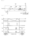
- FIG. 2 illustrates a detailed configuration diagram of the input power control unit 122 according to the first exemplary embodiment of the present disclosure.
- the input power control unit 122 may include a comparator 122a, an inverter 122b, a timing signal generator 122c, and a switching unit 122d.
- the comparator 122a may compare the voltage level V aux of the driving power detected by the driving power detection unit 121 with a preset reference voltage level V ref .
- the comparator 122a may include a first input terminal, a second input terminal, and an operational amplifier (OP).
- OP operational amplifier
- the first input terminal may be a non-inversion input terminal and the second input terminal may be an inversion input terminal.
- the first input terminal of the comparator 122a may receive the voltage level V aux of the driving power detected by the driving power detection unit 121 and the second input terminal of the comparator 122a may receive the preset reference voltage level V ref .
- the operational amplifier (OP) of the comparator 122a may compare the voltage level V aux of the driving power detected by the driving power detection unit 121 with the preset reference voltage level Vref and output a voltage signal Vout having a signal level depending on the comparison result to the inverter 122b.
- the inverter 122b may invert the level of the voltage signal output from the comparator 122a (for example, the level of V out illustrated in FIG. 3 ) and may output the inverted signal to the timing signal generator 122c.
- the timing signal generator 122c may be connected to the inverter 122b, generate a timing signal Vsw based on the detected voltage level V aux of the driving power, and output the generated timing signal Vsw to the switching unit 122d to control on/off operations of the switching unit 122d.
- the switching unit 122d may be turned on/off depending on the timing signal Vsw output from the timing signal generator 122C to supply or cut off the input power V AC to or from the main control unit 130.
- the main control unit 130 may control other controllers (for example, a PFC controller 123, a switching controller 116, and the like in the first exemplary embodiment of the present disclosure) which control each component of the primary side stage.
- the power supply 100 may control on/off operations of the switching unit 122d to control to supply or cut off the input power V AC to or from the main control unit 130, and thus may control the operation or the stopping of each component of the power supply 100.
- the switching unit 122d may be any switching element which may perform on/off switching operations, for example, but not limited to, a switching element such as MOSFET, a general-purpose transistor, and the like.
- FIG. 3 illustrates signal waveform diagrams of some parts of the power supply 100 according to the first exemplary embodiment of the present disclosure. As illustrated in FIG. 3 , the power supply 100 according to the first exemplary embodiment of the present disclosure may repeatedly perform operations of a normal operation mode and the standby mode.
- the timing signal generator 122c may generate the timing signal V sw of the level (high level in FIG. 3 ) which turns on the switching unit 122d and may output the generated timing signal V sw to the switching unit 122d.
- the switching unit 122d of the input power control unit 122 may be in a turn on state and thus may supply the rectified input power V AC to the main control unit 130.
- the power supply 100 may normally perform operations of each component of the power supply 100 depending on the entire control of the main control unit 130 in the case of the normal operation mode.
- the voltage level V 0 of the driving power may be increased due to control of the constant current.
- the voltage level V aux in the power detection unit 121 (auxiliary coil in the first embodiment) may be increased in proportion thereto, and when the voltage level V aux detected by the driving power detection unit 121 is equal to or more than the preset reference voltage level V ref according to the comparison result of the comparator 122a, the timing signal generator 122c may output the timing signal Vsw of the level (low level in FIG. 3 ), which turns off the switching unit 122d, to the switching unit 122d.
- the switching unit 122d may be turned off depending on the timing signal Vsw as described above to cut off the supply of the input power V AC to the main control unit 130, such that the power supply 100 according to the first exemplary embodiment of the present disclosure may stop all the operations of each component of the power supply 100 including the switching operation of the power switching unit 113.
- the timing signal generator 122c may output the timing signal Vsw of the level (high level in FIG. 3 ), which turns on the switching unit 122d, to the switching unit 122d.
- the switching unit 122d may be turned on depending on the timing signal Vsw as described above to supply the input power V AC to the main control unit 130, such that the power supply 100 according to the first exemplary embodiment of the present disclosure may perform operations of each component of the power supply 100 depending on the entire control of the main control unit 130.
- the power supply 100 may cut off the input power V AC itself depending on the voltage level V aux of the driving power by the above-mentioned configuration and operation process.
- the power supply 100 may stop the switching operation at the time of the standby mode and all the operations of each component of the power supply 100, and therefore may more reduce the standby power than the power supply (including the power supply of the burst mode type) which stops only the switching operation.
- the power supply 100 may, by the above-mentioned configuration and operation process, cut off the input power V AC itself when the voltage level Vaux of the driving power is equal to or more than the preset voltage level V ref .
- the power supply 100 may implement an over voltage protection (OVP) function without an additional OVP circuit, thereby, for example, but not limited to, reducing the number of parts, the size of the circuit, cost, and the like.
- OVP over voltage protection
- FIG. 4 illustrates a schematic circuit diagram of a power supply 200 according to a second exemplary embodiment of the present disclosure.
- the power supply 200 may include a primary side stage which is connected to input power and a secondary side stage which is connected to driving power V 0 .
- the power supply 200 may include a driving power supply unit 210 and a power supply control unit 220 which may be similar to the first exemplary embodiment of the present disclosure.
- the driving power supply unit 210 according to the second exemplary embodiment of the present disclosure is the same as, or similar to, the configuration of the first exemplary embodiment and therefore the detailed description thereof will be omitted. Therefore, components (for example, power supply control unit 220, and the like) different from the power supply 100 according to the first exemplary embodiment of the present disclosure and the operation processes thereof will be mainly described.
- the power supply control unit 220 may be connected to a rectifying unit 212.
- the power supply control unit 220 may include a driving power detection unit 221 and an input power control unit 222.
- the driving power detection unit 221 may be formed in the secondary side stage and the input power control unit 222 may be formed in the primary side stage.
- the driving power detection unit 221 may be formed in the secondary side stage.
- the driving power detection unit 221 may directly detect change in the voltage level V 0 of the secondary side driving power through a division resistor (not illustrated) formed in the secondary side stage.
- the driving power detection unit 121 according to the first exemplary embodiment of the present disclosure may indirectly detect the voltage level V 0 of the secondary side driving power using an auxiliary coil, and the like formed in the primary side.
- one or more parts for example, a photo coupler, and the like
- the voltage waveform signal may be directly detected in the secondary side, thereby more accurately detecting the voltage level V 0 of the driving voltage.
- the input power control unit 222 may control an operation of cutting off or supplying the input power V AC , and the like rectified by the rectifying unit 212 based on the voltage level V 0 of the driving power which is detected by the driving power detection unit 221.
- the power supply control unit 220 may control to detect change in the voltage level V 0 of the driving power, and to cut off the input power V AC when the detected voltage level V 0 of the driving power is equal to or more than a preset voltage level in the preset standby mode (for example, the no-load state or the light load state). Further, when the voltage level V 0 of the driving power detected in the standby mode is equal to or less than the preset voltage level, the power supply control unit 220 may control to supply the input power V AC .
- a preset voltage level in the preset standby mode for example, the no-load state or the light load state
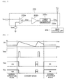
- FIG. 5 illustrates a detailed configuration diagram of the input power control unit 222 according to the first exemplary embodiment of the present disclosure.
- the input power control unit 222 may include a comparator 222a, an inverter 222b, a timing signal generator 222c, and a switching unit 222d.
- the comparator 222a may compare the voltage level V 0 of the driving power detected by the driving power detection unit 221 with a preset reference voltage level V ref .
- the comparator 222a may include a first input terminal, a second input terminal, and an operational amplifier (OP).
- the first input terminal may be a non-inversion input terminal and the second input terminal may be an inversion input terminal.
- the first input terminal of the comparator 222a may receive the voltage level V 0 of the driving power detected by the driving power detection unit 221 and the second input terminal of the comparator 222a may receive the preset reference voltage level V ref .
- the operational amplifier (OP) of the comparator 222a may compare the voltage level V 0 of the driving power detected by the driving power detection unit 221 with the preset reference voltage level V ref and output a voltage signal V out having a signal level depending on the comparison result to the inverter 222b.
- the inverter 222b may invert the level of the voltage signal output from the comparator 222a (for example, the level of the Vout illustrated in FIG. 6 ) and may output the inverted signal to the timing signal generator 222c.
- the timing signal generator 222c may be connected to the inverter 222, generate a timing signal Vsw based on the detected voltage level V 0 of the driving power detected by the driving power detection unit 221, and output the generated timing signal Vsw to the switching unit 222d to control the on/off operation of the switching unit 222d.
- the switching unit 222d may be turned on/off depending on the timing signal Vsw output from the timing signal generator 222C to supply or cut off the input power V AC to or from the main control unit 230.
- the main control unit 230 may be the same as, or similar to, the configuration and/or function of the main control unit 130 according to the first exemplary embodiment of the present disclosure and the description thereof will be omitted.
- the power supply 200 may control on/off operations of the switching unit 222d to control to supply or cut off the input power V AC to or from the main control unit 230, and thus may control the operation or the stopping of each component of the power supply 200.
- the switching unit 222d according to the second exemplary embodiment of the present disclosure may be any switching element which may perform on/off switching operations.
- FIG. 6 illustrates signal waveform diagrams of some parts of the power supply 200 according to the second exemplary embodiment of the present disclosure. Similar to the first exemplary embodiment of the present disclosure, the power supply 200 according to the second exemplary embodiment of the present disclosure may repeatedly perform operations of a normal operation mode and the standby mode.
- the timing signal generator 222c may generate the timing signal V sw of the level (high level in FIG. 6 ) which turns on the switching unit 222d and may output the generated timing signal V sw to the switching unit 222d.
- the switching unit 222d of the input power control unit 222 may be in a turn on state and thus may supply the rectified input power V AC to the main control unit 230.
- the power supply 200 according to the second exemplary embodiment of the present disclosure may normally perform operations of each component of the power supply 200 depending on the entire control of the main control unit 230 in the case of the normal operation mode.
- the voltage level V 0 of the driving power detected by the driving voltage detection unit 221 may be increased due to control of the constant current as illustrated in FIG. 6 .
- the timing signal generator 222c may output the timing signal Vsw of the level (low level in FIG. 6 ), which turns off the switching unit 222d, to the switching unit 222d.
- the switching unit 222d may be turned off depending on the timing signal Vsw as described above to cut off the supply of the input power V AC to the main control unit 230, such that the power supply 200 according to the second exemplary embodiment of the present disclosure may stop all the operations of each component of the power supply 200 including the switching operation of the power switching unit 213, similar to the first exemplary embodiment of the present disclosure.
- the timing signal generator 222c may output the timing signal V sw of the level (high level in FIG. 6 ), which turns on the switching unit 222d, to the switching unit 222d.
- the switching unit 222d may be turned on depending on the timing signal V sw as described above to supply the input power V AC to the main control unit 230, such that the power supply 200 according to the second exemplary embodiment of the present disclosure may perform the operations of each component of the power supply 200 similar to the first exemplary embodiment of the present disclosure.
- the power supply 200 may cut off the input power V AC itself depending on the voltage level V 0 of the driving power by the above-mentioned configuration and operation process.
- the power supply 200 may stop the switching operation at the time of the standby mode and all the operations of each component of the power supply 200, and therefore may more reduce the standby power than the power supply (including the power supply of the burst mode type) which stops only the switching operation.
- the power supply 200 may, by the above-mentioned configuration and operation process, cut off the input power V AC itself when the voltage level V 0 of the driving power is equal to or more than the preset voltage level V ref .
- the power supply 200 according to the second exemplary embodiment of the present disclosure may implement the OVP function without an additional OVP circuit, thereby , for example, but not limited to, reducing the number of parts, the size of the circuit, cost, and the like.
- the power supply 100 or 200 may cut off the input power depending on the voltage level of the driving power, thereby stopping the switching operation and the operations of each component of the power supply at the time of the standby mode. For example, it is possible to more reduce the standby power than the power supply (including the power supply of the burst mode type) which stops only the switching operation.
- the power supply 100 or 200 may cut off the input power itself when the voltage level V 0 of the driving power is equal to or more than the preset voltage level, such that the additional OVP function may be implemented without the OVP circuit. Therefore, it is possible to, for example, but not limited to, the number of parts, the size of the circuit, cost, and the like.
- the power supply 100 or 200 may reduce the number of parts, the size of the circuit, cost, and the like.
- control unit is not to be construed as exclusively designating hardware which may execute software and a microcontroller unit (MCU), digital signal processor (DSP) hardware, a read only memory (ROM) for storing software, a random access memory (RAM), a non-volatile storage device may be implicitly included without being limited.
- MCU microcontroller unit
- DSP digital signal processor
- ROM read only memory
- RAM random access memory
- elements expressed as a unit for performing specific functions includes any method of performing a specific function and these elements may include a combination of circuit elements performing the specific function or any type of software including a firmware, a microcode, and the like which are coupled with circuits suitable to perform software for performing the specific functions.
Landscapes
- Engineering & Computer Science (AREA)
- Power Engineering (AREA)
- Dc-Dc Converters (AREA)
Applications Claiming Priority (1)
| Application Number | Priority Date | Filing Date | Title |
|---|---|---|---|
| KR1020140007758A KR20150087598A (ko) | 2014-01-22 | 2014-01-22 | 전원 장치 |
Publications (1)
| Publication Number | Publication Date |
|---|---|
| EP2899863A1 true EP2899863A1 (fr) | 2015-07-29 |
Family
ID=52016536
Family Applications (1)
| Application Number | Title | Priority Date | Filing Date |
|---|---|---|---|
| EP14275255.9A Withdrawn EP2899863A1 (fr) | 2014-01-22 | 2014-12-11 | Alimentation électrique |
Country Status (3)
| Country | Link |
|---|---|
| US (1) | US9231485B2 (fr) |
| EP (1) | EP2899863A1 (fr) |
| KR (1) | KR20150087598A (fr) |
Cited By (2)
| Publication number | Priority date | Publication date | Assignee | Title |
|---|---|---|---|---|
| EP3591797A1 (fr) * | 2018-07-04 | 2020-01-08 | Self Electronics Co., Ltd. | Dispositif de commande de la consommation d'alimentation en veille pour système d'éclairage |
| EP3723252A1 (fr) * | 2019-04-10 | 2020-10-14 | Infineon Technologies Austria AG | Commande de convertisseur de puissance, convertisseur de puissance et procédé correspondant |
Families Citing this family (7)
| Publication number | Priority date | Publication date | Assignee | Title |
|---|---|---|---|---|
| US9380664B2 (en) * | 2014-10-21 | 2016-06-28 | General Electric Company | Microcontroller burst mode to maintain voltage supply during standby mode of a lighting system |
| WO2016205761A1 (fr) | 2015-06-19 | 2016-12-22 | Lutron Electronics Co., Inc. | Dispositif de commande de charge pour source lumineuse à diodes électroluminescentes |
| EP4072247B1 (fr) * | 2016-09-16 | 2024-03-27 | Lutron Technology Company LLC | Procede de commande de charge pour une source de lumière à diode électroluminescente doté de plusieurs modes de fonctionnement |
| KR102638182B1 (ko) * | 2018-12-26 | 2024-02-16 | 엘지전자 주식회사 | 영상표시장치 |
| JP7261909B2 (ja) * | 2019-05-31 | 2023-04-20 | 広東美的制冷設備有限公司 | 運転制御方法、回路、家電機器及びコンピュータ読み取り可能な記憶媒体 |
| CN113394862A (zh) * | 2020-03-12 | 2021-09-14 | Oppo广东移动通信有限公司 | 电源电路及充电设备 |
| US11553572B2 (en) * | 2020-03-31 | 2023-01-10 | Lutron Technology Company Llc | Power converter circuit for a lighting device |
Citations (6)
| Publication number | Priority date | Publication date | Assignee | Title |
|---|---|---|---|---|
| EP1742337A2 (fr) * | 2005-07-07 | 2007-01-10 | Power Integrations, Inc. | Procédé et appareil pour une réponse conditionnée dans le conditions de défauts dans une alimentation de puissance de commutation |
| EP1814213A1 (fr) * | 2006-01-30 | 2007-08-01 | Infineon Technologies AG | Circuit de commande d'alimentation à découpage, prodédé de commande d'alimentation à découpage et programme d'ordinateur |
| US20110169426A1 (en) * | 2009-07-16 | 2011-07-14 | Sadwick Laurence P | Fluorescent Lamp Power Supply |
| US20110194311A1 (en) * | 2010-02-09 | 2011-08-11 | Power Integrations, Inc. | Phase angle measurement of a dimming circuit for a switching power supply |
| KR20120014511A (ko) | 2010-08-09 | 2012-02-17 | 삼성전자주식회사 | 스위칭 모드 전원공급장치 및 이를 제어하는 방법 |
| US20120268039A1 (en) * | 2011-04-20 | 2012-10-25 | Liang Chen | Switching power supply with power feedback to keep lamp's brightness constant |
Family Cites Families (3)
| Publication number | Priority date | Publication date | Assignee | Title |
|---|---|---|---|---|
| JP2012216766A (ja) * | 2011-03-30 | 2012-11-08 | Sanken Electric Co Ltd | Led駆動装置及びled照明装置 |
| KR101357727B1 (ko) * | 2011-09-08 | 2014-02-06 | 주식회사 동부하이텍 | Led 구동장치를 위한 절연형 플라이백 변환회로 |
| KR101337349B1 (ko) * | 2012-03-21 | 2013-12-06 | 주식회사 동운아나텍 | 조명 구동 장치 및 그 방법 |
-
2014
- 2014-01-22 KR KR1020140007758A patent/KR20150087598A/ko not_active Withdrawn
- 2014-12-11 EP EP14275255.9A patent/EP2899863A1/fr not_active Withdrawn
- 2014-12-24 US US14/582,200 patent/US9231485B2/en not_active Expired - Fee Related
Patent Citations (6)
| Publication number | Priority date | Publication date | Assignee | Title |
|---|---|---|---|---|
| EP1742337A2 (fr) * | 2005-07-07 | 2007-01-10 | Power Integrations, Inc. | Procédé et appareil pour une réponse conditionnée dans le conditions de défauts dans une alimentation de puissance de commutation |
| EP1814213A1 (fr) * | 2006-01-30 | 2007-08-01 | Infineon Technologies AG | Circuit de commande d'alimentation à découpage, prodédé de commande d'alimentation à découpage et programme d'ordinateur |
| US20110169426A1 (en) * | 2009-07-16 | 2011-07-14 | Sadwick Laurence P | Fluorescent Lamp Power Supply |
| US20110194311A1 (en) * | 2010-02-09 | 2011-08-11 | Power Integrations, Inc. | Phase angle measurement of a dimming circuit for a switching power supply |
| KR20120014511A (ko) | 2010-08-09 | 2012-02-17 | 삼성전자주식회사 | 스위칭 모드 전원공급장치 및 이를 제어하는 방법 |
| US20120268039A1 (en) * | 2011-04-20 | 2012-10-25 | Liang Chen | Switching power supply with power feedback to keep lamp's brightness constant |
Cited By (2)
| Publication number | Priority date | Publication date | Assignee | Title |
|---|---|---|---|---|
| EP3591797A1 (fr) * | 2018-07-04 | 2020-01-08 | Self Electronics Co., Ltd. | Dispositif de commande de la consommation d'alimentation en veille pour système d'éclairage |
| EP3723252A1 (fr) * | 2019-04-10 | 2020-10-14 | Infineon Technologies Austria AG | Commande de convertisseur de puissance, convertisseur de puissance et procédé correspondant |
Also Published As
| Publication number | Publication date |
|---|---|
| US9231485B2 (en) | 2016-01-05 |
| KR20150087598A (ko) | 2015-07-30 |
| US20150207421A1 (en) | 2015-07-23 |
Similar Documents
| Publication | Publication Date | Title |
|---|---|---|
| US9231485B2 (en) | Power supply | |
| US9866108B2 (en) | PFC shutdown circuit for light load | |
| JP6255577B2 (ja) | 直流電源回路 | |
| JP5799537B2 (ja) | スイッチング電源装置の制御回路及びスイッチング電源装置 | |
| US9564813B2 (en) | Switching power-supply device | |
| US20120001599A1 (en) | Power Supply Circuit Capable of Handling Direct Current and Alternating Current and Power Supply Control Method | |
| US9991798B2 (en) | Constant on-time control for power converter | |
| JP2006094696A (ja) | 力率補正回路及びその出力電圧制御方法 | |
| US9093918B2 (en) | Control circuit for offline power converter without input capacitor | |
| US10938315B2 (en) | Control circuit for AC/DC converter | |
| JP5254876B2 (ja) | 力率改善型スイッチング電源装置 | |
| JP2009189158A (ja) | 電源装置の制御方法と電源装置 | |
| JP2011109871A (ja) | 直流電源装置 | |
| JP2012039736A (ja) | 電源装置 | |
| JP5277706B2 (ja) | スイッチング電源装置 | |
| KR101493520B1 (ko) | 이중출력 에스엠피에스 장치 | |
| JP2007236034A (ja) | 電源システム | |
| JP6499118B2 (ja) | 遊技機 | |
| JP2016093011A (ja) | スイッチング電源 | |
| JP6747766B2 (ja) | 電源装置およびその制御装置 | |
| JP2014079130A (ja) | 制御装置の電源回路 | |
| JP5971227B2 (ja) | スイッチング電源 | |
| JP6447593B2 (ja) | スイッチング電源装置及び半導体装置 | |
| WO2018043227A1 (fr) | Dispositif d'alimentation électrique de commutation et dispositif semi-conducteur | |
| JP6234242B2 (ja) | 電源装置 |
Legal Events
| Date | Code | Title | Description |
|---|---|---|---|
| PUAI | Public reference made under article 153(3) epc to a published international application that has entered the european phase |
Free format text: ORIGINAL CODE: 0009012 |
|
| 17P | Request for examination filed |
Effective date: 20141211 |
|
| AK | Designated contracting states |
Kind code of ref document: A1 Designated state(s): AL AT BE BG CH CY CZ DE DK EE ES FI FR GB GR HR HU IE IS IT LI LT LU LV MC MK MT NL NO PL PT RO RS SE SI SK SM TR |
|
| AX | Request for extension of the european patent |
Extension state: BA ME |
|
| 17P | Request for examination filed |
Effective date: 20160129 |
|
| RBV | Designated contracting states (corrected) |
Designated state(s): AL AT BE BG CH CY CZ DE DK EE ES FI FR GB GR HR HU IE IS IT LI LT LU LV MC MK MT NL NO PL PT RO RS SE SI SK SM TR |
|
| STAA | Information on the status of an ep patent application or granted ep patent |
Free format text: STATUS: THE APPLICATION HAS BEEN WITHDRAWN |
|
| 18W | Application withdrawn |
Effective date: 20161214 |