EP2901475B1 - Procédé de fabrication d'une interconnexion verticale traversante par dépôt autocatalytique de métal, et dispositif semiconducteur correspondant - Google Patents
Procédé de fabrication d'une interconnexion verticale traversante par dépôt autocatalytique de métal, et dispositif semiconducteur correspondant Download PDFInfo
- Publication number
- EP2901475B1 EP2901475B1 EP13841291.1A EP13841291A EP2901475B1 EP 2901475 B1 EP2901475 B1 EP 2901475B1 EP 13841291 A EP13841291 A EP 13841291A EP 2901475 B1 EP2901475 B1 EP 2901475B1
- Authority
- EP
- European Patent Office
- Prior art keywords
- silicon
- poly
- layer
- substrate
- via hole
- Prior art date
- Legal status (The legal status is an assumption and is not a legal conclusion. Google has not performed a legal analysis and makes no representation as to the accuracy of the status listed.)
- Active
Links
Images





Classifications
-
- H—ELECTRICITY
- H10—SEMICONDUCTOR DEVICES; ELECTRIC SOLID-STATE DEVICES NOT OTHERWISE PROVIDED FOR
- H10W—GENERIC PACKAGES, INTERCONNECTIONS, CONNECTORS OR OTHER CONSTRUCTIONAL DETAILS OF DEVICES COVERED BY CLASS H10
- H10W20/00—Interconnections in chips, wafers or substrates
- H10W20/01—Manufacture or treatment
- H10W20/021—Manufacture or treatment of interconnections within wafers or substrates
- H10W20/023—Manufacture or treatment of interconnections within wafers or substrates the interconnections being through-semiconductor vias
-
- H—ELECTRICITY
- H10—SEMICONDUCTOR DEVICES; ELECTRIC SOLID-STATE DEVICES NOT OTHERWISE PROVIDED FOR
- H10W—GENERIC PACKAGES, INTERCONNECTIONS, CONNECTORS OR OTHER CONSTRUCTIONAL DETAILS OF DEVICES COVERED BY CLASS H10
- H10W20/00—Interconnections in chips, wafers or substrates
- H10W20/01—Manufacture or treatment
- H10W20/031—Manufacture or treatment of conductive parts of the interconnections
- H10W20/069—Manufacture or treatment of conductive parts of the interconnections by forming self-aligned vias or self-aligned contact plugs
-
- H—ELECTRICITY
- H10—SEMICONDUCTOR DEVICES; ELECTRIC SOLID-STATE DEVICES NOT OTHERWISE PROVIDED FOR
- H10P—GENERIC PROCESSES OR APPARATUS FOR THE MANUFACTURE OR TREATMENT OF DEVICES COVERED BY CLASS H10
- H10P14/00—Formation of materials, e.g. in the shape of layers or pillars
- H10P14/20—Formation of materials, e.g. in the shape of layers or pillars of semiconductor materials
- H10P14/29—Formation of materials, e.g. in the shape of layers or pillars of semiconductor materials characterised by the substrates
- H10P14/2901—Materials
- H10P14/2902—Materials being Group IVA materials
- H10P14/2905—Silicon, silicon germanium or germanium
-
- H—ELECTRICITY
- H10—SEMICONDUCTOR DEVICES; ELECTRIC SOLID-STATE DEVICES NOT OTHERWISE PROVIDED FOR
- H10P—GENERIC PROCESSES OR APPARATUS FOR THE MANUFACTURE OR TREATMENT OF DEVICES COVERED BY CLASS H10
- H10P14/00—Formation of materials, e.g. in the shape of layers or pillars
- H10P14/20—Formation of materials, e.g. in the shape of layers or pillars of semiconductor materials
- H10P14/34—Deposited materials, e.g. layers
- H10P14/3402—Deposited materials, e.g. layers characterised by the chemical composition
- H10P14/3404—Deposited materials, e.g. layers characterised by the chemical composition being Group IVA materials
- H10P14/3411—Silicon, silicon germanium or germanium
-
- H—ELECTRICITY
- H10—SEMICONDUCTOR DEVICES; ELECTRIC SOLID-STATE DEVICES NOT OTHERWISE PROVIDED FOR
- H10P—GENERIC PROCESSES OR APPARATUS FOR THE MANUFACTURE OR TREATMENT OF DEVICES COVERED BY CLASS H10
- H10P14/00—Formation of materials, e.g. in the shape of layers or pillars
- H10P14/20—Formation of materials, e.g. in the shape of layers or pillars of semiconductor materials
- H10P14/34—Deposited materials, e.g. layers
- H10P14/3451—Structure
- H10P14/3452—Microstructure
- H10P14/3456—Polycrystalline
-
- H—ELECTRICITY
- H10—SEMICONDUCTOR DEVICES; ELECTRIC SOLID-STATE DEVICES NOT OTHERWISE PROVIDED FOR
- H10P—GENERIC PROCESSES OR APPARATUS FOR THE MANUFACTURE OR TREATMENT OF DEVICES COVERED BY CLASS H10
- H10P14/00—Formation of materials, e.g. in the shape of layers or pillars
- H10P14/40—Formation of materials, e.g. in the shape of layers or pillars of conductive or resistive materials
- H10P14/46—Formation of materials, e.g. in the shape of layers or pillars of conductive or resistive materials using a liquid
-
- H—ELECTRICITY
- H10—SEMICONDUCTOR DEVICES; ELECTRIC SOLID-STATE DEVICES NOT OTHERWISE PROVIDED FOR
- H10P—GENERIC PROCESSES OR APPARATUS FOR THE MANUFACTURE OR TREATMENT OF DEVICES COVERED BY CLASS H10
- H10P14/00—Formation of materials, e.g. in the shape of layers or pillars
- H10P14/60—Formation of materials, e.g. in the shape of layers or pillars of insulating materials
- H10P14/69—Inorganic materials
- H10P14/694—Inorganic materials composed of nitrides
- H10P14/6943—Inorganic materials composed of nitrides containing silicon
- H10P14/69433—Inorganic materials composed of nitrides containing silicon the material being a silicon nitride not containing oxygen, e.g. SixNy or SixByNz
-
- H—ELECTRICITY
- H10—SEMICONDUCTOR DEVICES; ELECTRIC SOLID-STATE DEVICES NOT OTHERWISE PROVIDED FOR
- H10W—GENERIC PACKAGES, INTERCONNECTIONS, CONNECTORS OR OTHER CONSTRUCTIONAL DETAILS OF DEVICES COVERED BY CLASS H10
- H10W20/00—Interconnections in chips, wafers or substrates
- H10W20/01—Manufacture or treatment
- H10W20/021—Manufacture or treatment of interconnections within wafers or substrates
- H10W20/023—Manufacture or treatment of interconnections within wafers or substrates the interconnections being through-semiconductor vias
- H10W20/0261—Manufacture or treatment of interconnections within wafers or substrates the interconnections being through-semiconductor vias characterised by the filling method or the material of the conductive fill
-
- H—ELECTRICITY
- H10—SEMICONDUCTOR DEVICES; ELECTRIC SOLID-STATE DEVICES NOT OTHERWISE PROVIDED FOR
- H10W—GENERIC PACKAGES, INTERCONNECTIONS, CONNECTORS OR OTHER CONSTRUCTIONAL DETAILS OF DEVICES COVERED BY CLASS H10
- H10W20/00—Interconnections in chips, wafers or substrates
- H10W20/01—Manufacture or treatment
- H10W20/031—Manufacture or treatment of conductive parts of the interconnections
- H10W20/032—Manufacture or treatment of conductive parts of the interconnections of conductive barrier, adhesion or liner layers
- H10W20/033—Manufacture or treatment of conductive parts of the interconnections of conductive barrier, adhesion or liner layers in openings in dielectrics
- H10W20/036—Manufacture or treatment of conductive parts of the interconnections of conductive barrier, adhesion or liner layers in openings in dielectrics the barrier, adhesion or liner layers being within a main fill metal
-
- H—ELECTRICITY
- H10—SEMICONDUCTOR DEVICES; ELECTRIC SOLID-STATE DEVICES NOT OTHERWISE PROVIDED FOR
- H10W—GENERIC PACKAGES, INTERCONNECTIONS, CONNECTORS OR OTHER CONSTRUCTIONAL DETAILS OF DEVICES COVERED BY CLASS H10
- H10W20/00—Interconnections in chips, wafers or substrates
- H10W20/01—Manufacture or treatment
- H10W20/031—Manufacture or treatment of conductive parts of the interconnections
- H10W20/032—Manufacture or treatment of conductive parts of the interconnections of conductive barrier, adhesion or liner layers
- H10W20/042—Manufacture or treatment of conductive parts of the interconnections of conductive barrier, adhesion or liner layers the barrier, adhesion or liner layers being seed or nucleation layers
- H10W20/044—Manufacture or treatment of conductive parts of the interconnections of conductive barrier, adhesion or liner layers the barrier, adhesion or liner layers being seed or nucleation layers for electroless plating
-
- H—ELECTRICITY
- H10—SEMICONDUCTOR DEVICES; ELECTRIC SOLID-STATE DEVICES NOT OTHERWISE PROVIDED FOR
- H10W—GENERIC PACKAGES, INTERCONNECTIONS, CONNECTORS OR OTHER CONSTRUCTIONAL DETAILS OF DEVICES COVERED BY CLASS H10
- H10W20/00—Interconnections in chips, wafers or substrates
- H10W20/01—Manufacture or treatment
- H10W20/031—Manufacture or treatment of conductive parts of the interconnections
- H10W20/056—Manufacture or treatment of conductive parts of the interconnections by filling conductive material into holes, grooves or trenches
- H10W20/057—Manufacture or treatment of conductive parts of the interconnections by filling conductive material into holes, grooves or trenches by selectively depositing, e.g. by using selective CVD or plating
-
- H—ELECTRICITY
- H10—SEMICONDUCTOR DEVICES; ELECTRIC SOLID-STATE DEVICES NOT OTHERWISE PROVIDED FOR
- H10W—GENERIC PACKAGES, INTERCONNECTIONS, CONNECTORS OR OTHER CONSTRUCTIONAL DETAILS OF DEVICES COVERED BY CLASS H10
- H10W20/00—Interconnections in chips, wafers or substrates
- H10W20/01—Manufacture or treatment
- H10W20/031—Manufacture or treatment of conductive parts of the interconnections
- H10W20/064—Manufacture or treatment of conductive parts of the interconnections by modifying the conductivity of conductive parts, e.g. by alloying
- H10W20/065—Manufacture or treatment of conductive parts of the interconnections by modifying the conductivity of conductive parts, e.g. by alloying by making at least a portion of the conductive part non-conductive, e.g. by oxidation
-
- H—ELECTRICITY
- H10—SEMICONDUCTOR DEVICES; ELECTRIC SOLID-STATE DEVICES NOT OTHERWISE PROVIDED FOR
- H10W—GENERIC PACKAGES, INTERCONNECTIONS, CONNECTORS OR OTHER CONSTRUCTIONAL DETAILS OF DEVICES COVERED BY CLASS H10
- H10W20/00—Interconnections in chips, wafers or substrates
- H10W20/01—Manufacture or treatment
- H10W20/031—Manufacture or treatment of conductive parts of the interconnections
- H10W20/067—Manufacture or treatment of conductive parts of the interconnections by modifying the pattern of conductive parts
-
- H—ELECTRICITY
- H10—SEMICONDUCTOR DEVICES; ELECTRIC SOLID-STATE DEVICES NOT OTHERWISE PROVIDED FOR
- H10W—GENERIC PACKAGES, INTERCONNECTIONS, CONNECTORS OR OTHER CONSTRUCTIONAL DETAILS OF DEVICES COVERED BY CLASS H10
- H10W20/00—Interconnections in chips, wafers or substrates
- H10W20/20—Interconnections within wafers or substrates, e.g. through-silicon vias [TSV]
-
- H—ELECTRICITY
- H10—SEMICONDUCTOR DEVICES; ELECTRIC SOLID-STATE DEVICES NOT OTHERWISE PROVIDED FOR
- H10W—GENERIC PACKAGES, INTERCONNECTIONS, CONNECTORS OR OTHER CONSTRUCTIONAL DETAILS OF DEVICES COVERED BY CLASS H10
- H10W70/00—Package substrates; Interposers; Redistribution layers [RDL]
- H10W70/01—Manufacture or treatment
- H10W70/05—Manufacture or treatment of insulating or insulated package substrates, or of interposers, or of redistribution layers
- H10W70/095—Manufacture or treatment of insulating or insulated package substrates, or of interposers, or of redistribution layers of vias therein
-
- H—ELECTRICITY
- H10—SEMICONDUCTOR DEVICES; ELECTRIC SOLID-STATE DEVICES NOT OTHERWISE PROVIDED FOR
- H10W—GENERIC PACKAGES, INTERCONNECTIONS, CONNECTORS OR OTHER CONSTRUCTIONAL DETAILS OF DEVICES COVERED BY CLASS H10
- H10W70/00—Package substrates; Interposers; Redistribution layers [RDL]
- H10W70/60—Insulating or insulated package substrates; Interposers; Redistribution layers
- H10W70/611—Insulating or insulated package substrates; Interposers; Redistribution layers for connecting multiple chips together
-
- H—ELECTRICITY
- H10—SEMICONDUCTOR DEVICES; ELECTRIC SOLID-STATE DEVICES NOT OTHERWISE PROVIDED FOR
- H10W—GENERIC PACKAGES, INTERCONNECTIONS, CONNECTORS OR OTHER CONSTRUCTIONAL DETAILS OF DEVICES COVERED BY CLASS H10
- H10W70/00—Package substrates; Interposers; Redistribution layers [RDL]
- H10W70/60—Insulating or insulated package substrates; Interposers; Redistribution layers
- H10W70/62—Insulating or insulated package substrates; Interposers; Redistribution layers characterised by their interconnections
- H10W70/63—Vias, e.g. via plugs
- H10W70/635—Through-vias
-
- H—ELECTRICITY
- H10—SEMICONDUCTOR DEVICES; ELECTRIC SOLID-STATE DEVICES NOT OTHERWISE PROVIDED FOR
- H10W—GENERIC PACKAGES, INTERCONNECTIONS, CONNECTORS OR OTHER CONSTRUCTIONAL DETAILS OF DEVICES COVERED BY CLASS H10
- H10W72/00—Interconnections or connectors in packages
- H10W72/01—Manufacture or treatment
- H10W72/013—Manufacture or treatment of die-attach connectors
- H10W72/01315—Forming coatings
-
- H—ELECTRICITY
- H10—SEMICONDUCTOR DEVICES; ELECTRIC SOLID-STATE DEVICES NOT OTHERWISE PROVIDED FOR
- H10W—GENERIC PACKAGES, INTERCONNECTIONS, CONNECTORS OR OTHER CONSTRUCTIONAL DETAILS OF DEVICES COVERED BY CLASS H10
- H10W72/00—Interconnections or connectors in packages
- H10W72/01—Manufacture or treatment
- H10W72/013—Manufacture or treatment of die-attach connectors
- H10W72/01331—Manufacture or treatment of die-attach connectors using blanket deposition
- H10W72/01333—Manufacture or treatment of die-attach connectors using blanket deposition in liquid form, e.g. spin coating, spray coating or immersion coating
- H10W72/01335—Manufacture or treatment of die-attach connectors using blanket deposition in liquid form, e.g. spin coating, spray coating or immersion coating by plating, e.g. electroless plating or electroplating
-
- H—ELECTRICITY
- H10—SEMICONDUCTOR DEVICES; ELECTRIC SOLID-STATE DEVICES NOT OTHERWISE PROVIDED FOR
- H10W—GENERIC PACKAGES, INTERCONNECTIONS, CONNECTORS OR OTHER CONSTRUCTIONAL DETAILS OF DEVICES COVERED BY CLASS H10
- H10W70/00—Package substrates; Interposers; Redistribution layers [RDL]
- H10W70/60—Insulating or insulated package substrates; Interposers; Redistribution layers
- H10W70/62—Insulating or insulated package substrates; Interposers; Redistribution layers characterised by their interconnections
- H10W70/65—Shapes or dispositions of interconnections
-
- H—ELECTRICITY
- H10—SEMICONDUCTOR DEVICES; ELECTRIC SOLID-STATE DEVICES NOT OTHERWISE PROVIDED FOR
- H10W—GENERIC PACKAGES, INTERCONNECTIONS, CONNECTORS OR OTHER CONSTRUCTIONAL DETAILS OF DEVICES COVERED BY CLASS H10
- H10W70/00—Package substrates; Interposers; Redistribution layers [RDL]
- H10W70/60—Insulating or insulated package substrates; Interposers; Redistribution layers
- H10W70/62—Insulating or insulated package substrates; Interposers; Redistribution layers characterised by their interconnections
- H10W70/65—Shapes or dispositions of interconnections
- H10W70/654—Top-view layouts
-
- H—ELECTRICITY
- H10—SEMICONDUCTOR DEVICES; ELECTRIC SOLID-STATE DEVICES NOT OTHERWISE PROVIDED FOR
- H10W—GENERIC PACKAGES, INTERCONNECTIONS, CONNECTORS OR OTHER CONSTRUCTIONAL DETAILS OF DEVICES COVERED BY CLASS H10
- H10W72/00—Interconnections or connectors in packages
- H10W72/01—Manufacture or treatment
- H10W72/019—Manufacture or treatment of bond pads
- H10W72/01931—Manufacture or treatment of bond pads using blanket deposition
- H10W72/01933—Manufacture or treatment of bond pads using blanket deposition in liquid form, e.g. spin coating, spray coating or immersion coating
- H10W72/01935—Manufacture or treatment of bond pads using blanket deposition in liquid form, e.g. spin coating, spray coating or immersion coating by plating, e.g. electroless plating or electroplating
-
- H—ELECTRICITY
- H10—SEMICONDUCTOR DEVICES; ELECTRIC SOLID-STATE DEVICES NOT OTHERWISE PROVIDED FOR
- H10W—GENERIC PACKAGES, INTERCONNECTIONS, CONNECTORS OR OTHER CONSTRUCTIONAL DETAILS OF DEVICES COVERED BY CLASS H10
- H10W72/00—Interconnections or connectors in packages
- H10W72/90—Bond pads, in general
- H10W72/921—Structures or relative sizes of bond pads
- H10W72/922—Bond pads being integral with underlying chip-level interconnections
-
- H—ELECTRICITY
- H10—SEMICONDUCTOR DEVICES; ELECTRIC SOLID-STATE DEVICES NOT OTHERWISE PROVIDED FOR
- H10W—GENERIC PACKAGES, INTERCONNECTIONS, CONNECTORS OR OTHER CONSTRUCTIONAL DETAILS OF DEVICES COVERED BY CLASS H10
- H10W72/00—Interconnections or connectors in packages
- H10W72/90—Bond pads, in general
- H10W72/921—Structures or relative sizes of bond pads
- H10W72/922—Bond pads being integral with underlying chip-level interconnections
- H10W72/9223—Bond pads being integral with underlying chip-level interconnections with redistribution layers [RDL]
-
- H—ELECTRICITY
- H10—SEMICONDUCTOR DEVICES; ELECTRIC SOLID-STATE DEVICES NOT OTHERWISE PROVIDED FOR
- H10W—GENERIC PACKAGES, INTERCONNECTIONS, CONNECTORS OR OTHER CONSTRUCTIONAL DETAILS OF DEVICES COVERED BY CLASS H10
- H10W72/00—Interconnections or connectors in packages
- H10W72/90—Bond pads, in general
- H10W72/921—Structures or relative sizes of bond pads
- H10W72/922—Bond pads being integral with underlying chip-level interconnections
- H10W72/9226—Bond pads being integral with underlying chip-level interconnections with via interconnections
-
- H—ELECTRICITY
- H10—SEMICONDUCTOR DEVICES; ELECTRIC SOLID-STATE DEVICES NOT OTHERWISE PROVIDED FOR
- H10W—GENERIC PACKAGES, INTERCONNECTIONS, CONNECTORS OR OTHER CONSTRUCTIONAL DETAILS OF DEVICES COVERED BY CLASS H10
- H10W72/00—Interconnections or connectors in packages
- H10W72/90—Bond pads, in general
- H10W72/921—Structures or relative sizes of bond pads
- H10W72/923—Bond pads having multiple stacked layers
-
- H—ELECTRICITY
- H10—SEMICONDUCTOR DEVICES; ELECTRIC SOLID-STATE DEVICES NOT OTHERWISE PROVIDED FOR
- H10W—GENERIC PACKAGES, INTERCONNECTIONS, CONNECTORS OR OTHER CONSTRUCTIONAL DETAILS OF DEVICES COVERED BY CLASS H10
- H10W72/00—Interconnections or connectors in packages
- H10W72/90—Bond pads, in general
- H10W72/941—Dispositions of bond pads
- H10W72/944—Dispositions of multiple bond pads
-
- H—ELECTRICITY
- H10—SEMICONDUCTOR DEVICES; ELECTRIC SOLID-STATE DEVICES NOT OTHERWISE PROVIDED FOR
- H10W—GENERIC PACKAGES, INTERCONNECTIONS, CONNECTORS OR OTHER CONSTRUCTIONAL DETAILS OF DEVICES COVERED BY CLASS H10
- H10W72/00—Interconnections or connectors in packages
- H10W72/90—Bond pads, in general
- H10W72/951—Materials of bond pads
- H10W72/952—Materials of bond pads comprising metals or metalloids, e.g. PbSn, Ag or Cu
Definitions
- This invention is related to through silicon via (TSV) technology, and in particular to providing metal vias with high aspect ratio in substrates together with self-aligned routing structures on the surface of the substrate, in order to make so called interposers.
- TSV through silicon via
- electrical lead patterns or routings
- Such routing patterns can be fairly complicated to process and often require several lithographic steps, and/or CMP (Chemical Mechanical Polishing) which is an expensive procedure.
- CMP Chemical Mechanical Polishing
- Wet etching of seed layer and barrier layer is quite often complex, if it has to be performed after the Cu electroplating. See e.g. an article by Richard et al, "Barrier and Copper Seed Layer Wet Etching" in Solid State Phenomena, Vol. 103-104, 2005, pp 361-364 .
- EP 1 987 535 (Silex ) there is disclosed a method of making metal vias using gold. In view of gold being a very expensive material this method is not particularly economically feasible.
- Alchimer in WO 2010/133550 discloses a method of making a coated substrate, wherein a cavity is made in a substrate surface by etching. An insulating dielectric layer is deposited on the substrate surface, and then polysilicon, which is in situ doped with phosphorous, is deposited on the dielectric layer. Finally, copper is electrodeposited on the doped polysilicon. No Cu diffusion barrier is provided in this process.
- US 2005/150683 A1 discloses a Si interposer with through-substrate vias and a redistribution layer, comprising a sidewall insulation, e.g. oxide, a seed layer, e.g. poly, a conductor layer, e.g. Ni, and a barrier layer formed of electroless Ni.
- a sidewall insulation e.g. oxide
- a seed layer e.g. poly
- a conductor layer e.g. Ni
- barrier layer formed of electroless Ni.
- US 2009/160058 A1 discloses a Cu TSV integral with a redistribution layer.
- the object of the invention is to provide a method that overcomes the drawbacks indicated in the background, and enables the provision of conformal metal coatings with good adhesion in combination with Cu diffusion barrier layer, in high aspect ratio via holes, and in the same process provides self-aligned routing patterns with fewer steps than according to the prior art methods. This is achieved by a method based on electroless plating using open via holes, and is defined in claim 1.
- the method provides "self alignment" of metal routing patterns and good adhesion of the materials, since these patterns are defined in polysilicon on which barrier and seed layers are deposited selectively, and no etch of seed layer or barrier is required before or after the final metallization is provided.
- the electroless plating is performed in open via holes i.e. holes extending through the entire substrate, which makes it easy to provide the necessary agitation of plating solutions.
- the invention provides for electroplating of the metallization, using the poly-silicon as conduction layer, suitably protected by oxide to leave only desired areas exposed to plating.
- the invention provides a method of making a substrate-through metal via having a high aspect ratio, in a semiconductor substrate, and a metal pattern on the substrate surface, comprising:
- the invention also provides a semiconductor device comprising:
- a major advantage with the present invention is that it enables batch processing of wafers as opposed to prior art methods where individual wafers are processed one by one, which renders the process very cost effective through simultaneous double sided processing.
- Open vias improves the wetting capability during plating, overcoming drawbacks with prior art methods. It also enables manufacture of rigid TSV wafers having hermetically sealed via structures.
- the present invention provides a method of providing a conformal metal coating in high aspect ratio vias. This is achieved by using an electroless deposition of copper on a base of n-type doped (e.g. Phophorous) poly-silicon, optionally with a Ni barrier layer also provided by electroless deposition. Additionally, in the same deposition step, self-aligned routing is provided.
- n-type doped (e.g. Phophorous) poly-silicon optionally with a Ni barrier layer also provided by electroless deposition.
- electroless plating as used herein is equivalent to "chemical plating”.
- a substrate 10 preferably a wafer of a semiconductor material, suitably single crystalline silicon, is provided, although other materials common in MEMS/IC processing is usable.
- a through-hole 12 is made in the substrate by commonly known processes, e.g. by lithography involving providing a resist on the surface, exposing a pattern corresponding to the hole(s) to be made, and developing the resist (not shown). Then an etch is applied whereby a hole 12 is made.
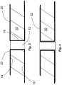
- the entire substrate is passivated, preferably by oxidation, as shown in Fig. 3 , such that the surfaces 14, 16 of the substrate and also the walls 18 in the hole 12 are covered with a thin oxide layer 20.
- the thickness of the oxide is > 0,5 ⁇ m, typically about 1 ⁇ m.
- poly-silicon is deposited over the substrate to form a poly-silicon layer 22 covering the entire substrate including the walls in the hole 12, as can be seen in Fig. 4 .
- a conformal deposition technique such as LPCVD (Low Pressure Chemical Vapour Deposition) is preferred due to its good uniform coverage on the high aspect ration via holes.
- the poly-silicon is doped, preferably with phophorous, either in the deposition process or subsequently by a dopant diffusion or ion implanting process with subsequent anneal/activation.
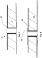
- the poly-silicon is patterned using similar or the same techniques as previously, i.e. lithography for providing an etch mask so as to enable etching away undesired portions of the poly-silicon to leave only areas 24 of the poly-silicon 22 suitable for plating, Fig. 5 . These areas can be routing patterns or other structure on the surface.
- a seed layer for later plating is to be provided on the poly-silicon areas that remain, suitably by an electroless deposition of Cu.
- a barrier layer 26 against Cu diffusion is required and such a barrier is therefore first applied by electroless deposition of Ni or Ni alloy, that selectively will coat the poly-silicon, see Fig. 6 .
- Cu is subsequently deposited by electroless plating on the Ni.
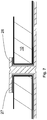
- a high temperature silicidation is performed, e.g. by an RTA process (Rapid Thermal Annealing), suitably at 300-700 °C.
- RTA process Rapid Thermal Annealing
- This silicide layer is shown as 27 in Fig. 7 as a thicker interface layer.
- TSV processes include starting substrates with metal which makes them more limited in terms of what processes and temperatures can be used.
- a thicker copper layer 28 is plated on the barrier/seed layer 27 by an electroless process whereby the hole is optionally eventually closed and a solid metal via formed in the same process step as the desired routings or other structures defined on the surface of the substrate, see Fig. 7 .
- this embodiment entails processing on wafers exhibiting topography (i.e. holes) which renders it slightly more complicated, although it still results in advantageous features compared to the prior art.
- Figs. 8-14 In another embodiment, which is still more advantageous in that it eliminates the need for lithography on non-flat surfaces, the process sequence is slightly altered, reference is made to Figs. 8-14 .
- This embodiment allows smaller feature sizes in the routing structures.
- line widths i.e. Cu RDLs
- the wafers are patterned after the holes are made, which renders the process more difficult.
- the spacing between lines can be made very small, in the same range as the above mentioned line widths.
- a substrate wafer 30 is provided as previously, but now the entire wafer is oxidized 32, the thickness of the oxide being > 0,5 ⁇ m, typically about 1-3 ⁇ m.
- the oxide is covered with a protective SiN layer 34 which is comparatively thick (i.e. >0,1 ⁇ m thick). The SiN will protect the oxide in later process steps.
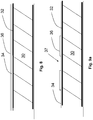
- a fairly thick (> 2 ⁇ m thick) poly-silicon layer 36 is deposited over the entire wafer, as shown in Fig. 8 .
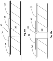
- the poly-silicon 36 on the flat substrate i.e. without topography (no holes) is patterned by lithography to provide a structure that corresponds to routings on the surface, if required, and also an opening 37 is provided for etching the through-hole, see Figs. 9a-b (the hole to be made is shown in broken lines in Fig. 9b ).
- a further SiN layer 38 is applied, this layer being thinner than the protective SiN layer 34 applied previously, for reasons that will be apparent below.
- an etch is applied to the wafer through the mask whereby a hole 39 is etched through the wafer, Fig. 10a .
- a localized thermal oxidation is performed whereby only the exposed silicon surfaces are oxidized, i.e. the walls of the through-hole are coated with oxide 40, Fig. 10b , the thickness of the oxide being > 0,5 ⁇ m, typically about 1-3 ⁇ m, while the surface areas protected with SiN will not become oxidized.
- etch is applied which will remove the SiN 38 on the horizontal surfaces leaving the first SiN layer 34 and the poly-silicon 36 exposed, as shown in Fig. 11 .
- poly-silicon in order to be able to provide a good seed-layer that ascertains the final coating with metal both to fill the hole and to provide the copper on the routing structures, and most importantly provides electrical connection between via and routings, poly-silicon must be provided on the walls of the hole, and therefore poly-silicon 41 is deposited again over the entire wafer, as shown in Fig. 12 .
- the poly-silicon layer 41 is typically thinner than the poly-silicon 36 provided earlier in the process.
- This deposition process will cover the wafer surface, either only one side or optionally both sides, with poly-silicon, and thus it must selectively be removed so as to expose only the poly-silicon 36 which defines the routing structures, otherwise the entire surface would subsequently be plated with metal.
- a high biased RIE is applied to the surface, which removes the second deposition of thinner poly-silicon down to the nitride/oxide layer except for the areas covered by the first thicker deposited poly-silicon 36, whereby the structure shown in Fig. 13a is arrived at.
- the etching process is set up to only etch the second poly-silicon layer on the field surfaces, but does not attack the second, vertically provided poly-silicon on the via walls.
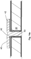
- a very important feature is what is shown in the encircled portion, magnified in Fig. 13b , namely, that despite the presence of a "break" in the continuity of the poly-silicon layers 34, 41, it will be possible to provide a continuous Ni layer 42 by electroless plating which is made selectively on the poly-silicon surfaces. In contrast to electro-plating the electroless plating will cause the Ni to grow such that the Ni deposited on the two different poly-silicon surfaces eventually will "bridge" the gap and form a continuous layer of the deposited Ni.
- the Ni layer is shown in Fig. 13c .
- the Ni layer is provided as a Cu diffusion barrier on which subsequently a copper can be plated so as to fill the hole and provide copper routings on the wafer surface.
- the Ni is shown as layer 42 in Fig. 14a
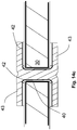
- the plated Cu is shown as 43. It is an important feature of the invention that the plated Cu 43 is continuous, i.e. there is no distinct interface between the horizontally applied Cu and the Cu inside the via, see also Fig. 14c , where the Cu layer is continuous and extends on both sides. Again, silicidation to form Si x Ni y , as disclosed previously, is performed for improved adhesion.
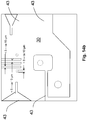
- Fig. 14b shows the structure of Fig. 14a from above, i.e. a substrate 30 wherein the routing structure 43 is shown, and obtainable dimensions are indicated.
- the preferred electroless Ni plating is commercially available and is phosphorous based, and therefore, in order to obtain the best results, the poly-Si is preferably doped with phosphorous.
- the poly-Si can either be in situ doped or it can be doped in a separate doping process involving annealing.
- the methods disclosed herein in a further embodiment, can be supplemented with an additional electroplating step, that does not generate bubbles and is used for conventional TSV from Cu, and which will be described in detail below with reference to Fig. 15 .
- the poly-silicon 36 deposited in a previous step is not patterned and etched to define routings, as described in connection with e.g. Fig. 9a , instead the poly-silicon 36 is covered selectively with an insulating material 46, e.g. oxide, according to a desired pattern to define the routing pattern, and will thus cover only the portions not defining the routing.
- an insulating material 46 e.g. oxide
- the oxide 46 protects the poly-silicon from being plated (electroless Ni and Cu seed layers), and only the desired routing pattern and via structures will be coated with metal.
- the poly-silicon layer will act as the means to transport current to each location where electroplating is desired.
- the entire wafer is immersed in a plating bath 47 and a negative potential (DC) is applied to the polysilicon, most often along the wafer edge, so as to provide for reduction of metal onto the locations where the plating is to occur.
- DC negative potential
- the via structure is of the type disclosed in EP 2 165 362 ( ⁇ STC Aerospace AB), referred to as XiViaTM.
- This via structure comprises a wide part and a narrow part with sloping surfaces. The narrow part is about 25 ⁇ m of the wafer thickness.
- the difference between an ordinary via and the XiViaTM type of via is schematically illustrated in Fig. 16 (dimensions not to scale). Thus, in Fig.
- the via (XiViaTM) shown in Fig. 16b will close only at the stricture S and thus no void is formed and the hermeticity is guaranteed.
- the via comprises a narrow and a wide path it is very easy to obtain a continuous plated Cu layer, that will close (at least) the narrow part of the via and in the process provide a hermetically sealed structure with no joints.
Landscapes
- Internal Circuitry In Semiconductor Integrated Circuit Devices (AREA)
- Electrodes Of Semiconductors (AREA)
- Chemically Coating (AREA)
Claims (15)
- Procédé de fabrication d'une interconnexion métallique traversant le substrat ayant un facteur de forme élevé, dans un substrat semi-conducteur, et d'un motif métallique sur la surface de substrat, comprenant :a) la fourniture d'un substrat semi-conducteur (10, 30) ;b) le dépôt d'un premier polysilicium (22, 36) sur le substrat (10, 30) ;c) le traçage d'un motif dans le premier polysilicium (22, 36) sur la surface de substrat ;d) le dépôt sélectif de Ni sur le premier polysilicium (22, 36) dans lequel est tracé un motif par un processus autocatalytique, ete) la fourniture d'une couche barrière intermédiaire de siliciure SixNiy par siliciuration du Ni déposé ;la fabrication d'un trou d'interconnexion à travers le substrat, dans lequel les parois dans le trou (12, 39) sont soumises au même traitement que dans les étapes b), d) et e) ; et
le dépôt de Cu sur le Ni par un processus de dépôt. - Procédé selon la revendication 1, dans lequel la couche barrière de siliciure SixNiy est fournie par chauffage du Ni déposé à environ 300 à 700 °C.
- Procédé selon la revendication 1 ou 2, dans lequel le traçage de motif du premier polysilicium (36) est obtenu par élimination par gravure des portions non souhaitées ou par recouvrement avec un matériau isolant.
- Procédé selon la revendication 1, 2 ou 3, dans lequel le dépôt de Cu comprend un dépôt autocatalytique, et éventuellement un électroplacage ultérieur.
- Procédé selon l'une quelconque des revendications précédentes, dans lequel le dépôt de Cu est poursuivi jusqu'à la fermeture du trou d'interconnexion (12, 39).
- Procédé selon l'une quelconque des revendications précédentes, comprenant en outre l'oxydation du substrat avant le dépôt du premier polysilicium (36).
- Procédé selon la revendication 6, comprenant en outre l'oxydation des parois dans le trou d'interconnexion (12, 39).
- Procédé selon la revendication 6 ou 7, dans lequel le trou (12) est réalisé avant l'étape d'oxydation du substrat (10).
- Procédé selon la revendication 1, dans lequel le trou (39) est réalisé après l'étape de traçage de motif dans le premier polysilicium.
- Procédé selon la revendication 9, comprenant en outre l'oxydation du substrat (30) et le recouvrement de l'oxyde avec une première couche protectrice (34) de SiN avant le dépôt du premier polysilicium (36).
- Procédé selon la revendication 10, comprenant en outre, après la fabrication du trou d'interconnexion (39), l'oxydation des parois dans le trou d'interconnexion (39), dans lequel la soumission des parois dans le trou (39) au même traitement que dans l'étape b) comprend la fourniture d'une seconde couche de polysilicium (41) sur la couche d'oxyde dans le trou (39), en fournissant ainsi un espace entre le polysilicium (41) sur les parois du trou d'interconnexion (39) et le premier polysilicium (36) déposé.
- Procédé selon la revendication 11, comprenant en outre le dépôt d'une couche de SiN supplémentaire (38) sur le polysilicium avant la fabrication du trou d'interconnexion (39), la couche de SiN supplémentaire (38) étant plus mince que la première couche de SiN (34).
- Procédé selon la revendication 12, comprenant en outre :l'élimination de la couche de SiN supplémentaire (38) du substrat (30) après la fabrication du trou d'interconnexion (39), pour exposer le premier polysilicium (36), dans lequel le second polysilicium (41) est plus mince que le premier polysilicium (36) ; etl'application ultérieure d'une gravure pour éliminer le second polysilicium (41) plus mince sur les surfaces de champs, mais pas le second polysilicium (41) prévu verticalement sur les parois d'interconnexion, en fournissant ainsi un espace entre le polysilicium sur les parois du trou d'interconnexion et le premier polysilicium (36) déposé plus épais,dans lequel le Ni déposé par dépôt autocatalytique sur les deux surfaces de polysilicium (36, 41) différentes enjambe l'espace et forme une couche continue.
- Procédé selon la revendication 13, comprenant en outre l'application d'une couche de germe sur le Ni, dans lequel le dépôt de Cu sur le Ni par le processus de dépôt comprend le dépôt sélectif de Cu sur ladite couche de germe.
- Dispositif à semi-conducteur, comprenant :une tranche de substrat (10, 30) de silicium ;un trou d'interconnexion (12, 39) à travers le substrat (10, 30) ;une couche d'oxyde (20, 32, 40) sur la surface de substrat et sur les parois du trou d'interconnexion (12, 39) ;une couche de polysilicium (22, 36, 41) sur la couche d'oxyde (20, 32, 40) sur la surface de tranche et sur les parois du trou d'interconnexion (12, 39), le polysilicium (22, 36) formant des structures de redistribution/routage latérales sur la surface de tranche ;une couche barrière intermédiaire de siliciure SixNiy sur le polysilicium (22, 36, 41) ;une barrière de diffusion de Ni (26, 42) sur le siliciure, la barrière de diffusion de Ni (26, 42) recouvrant en continu les structures de redistribution/routage latérales et les surfaces du trou d'interconnexion (12, 39) ; etune couche de Cu continue (28, 43) recouvrant la barrière de diffusion de Ni (26, 42) sur les structures de redistribution/routage latérales et sur les surfaces dans le trou d'interconnexion (12, 39).
Applications Claiming Priority (2)
| Application Number | Priority Date | Filing Date | Title |
|---|---|---|---|
| SE1251089A SE538062C2 (sv) | 2012-09-27 | 2012-09-27 | Kemiskt pläterad metallvia genom kisel |
| PCT/SE2013/051124 WO2014051511A2 (fr) | 2012-09-27 | 2013-09-27 | Trou d'interconnexion de silicium traversant un métal autocatalytique |
Publications (3)
| Publication Number | Publication Date |
|---|---|
| EP2901475A2 EP2901475A2 (fr) | 2015-08-05 |
| EP2901475A4 EP2901475A4 (fr) | 2016-05-04 |
| EP2901475B1 true EP2901475B1 (fr) | 2020-02-26 |
Family
ID=50389103
Family Applications (1)
| Application Number | Title | Priority Date | Filing Date |
|---|---|---|---|
| EP13841291.1A Active EP2901475B1 (fr) | 2012-09-27 | 2013-09-27 | Procédé de fabrication d'une interconnexion verticale traversante par dépôt autocatalytique de métal, et dispositif semiconducteur correspondant |
Country Status (5)
| Country | Link |
|---|---|
| US (2) | US9514985B2 (fr) |
| EP (1) | EP2901475B1 (fr) |
| HK (1) | HK1213089A1 (fr) |
| SE (1) | SE538062C2 (fr) |
| WO (1) | WO2014051511A2 (fr) |
Families Citing this family (14)
| Publication number | Priority date | Publication date | Assignee | Title |
|---|---|---|---|---|
| US9716192B2 (en) | 2014-03-28 | 2017-07-25 | International Business Machines Corporation | Method for fabricating a photovoltaic device by uniform plating on emitter-lined through-wafer vias and interconnects |
| JP6362254B2 (ja) * | 2014-05-12 | 2018-07-25 | 国立大学法人東北大学 | 半導体装置およびその製造方法 |
| JP6363868B2 (ja) * | 2014-05-12 | 2018-07-25 | 国立大学法人東北大学 | 半導体装置およびその製造方法 |
| WO2017029822A1 (fr) * | 2015-08-18 | 2017-02-23 | 三菱電機株式会社 | Dispositif à semi-conducteur |
| KR102501675B1 (ko) | 2018-07-13 | 2023-02-17 | 삼성전자주식회사 | 반도체 장치 및 그 제조 방법 |
| IT201900006736A1 (it) | 2019-05-10 | 2020-11-10 | Applied Materials Inc | Procedimenti di fabbricazione di package |
| CN112289688B (zh) * | 2019-07-22 | 2024-05-07 | 盛合晶微半导体(江阴)有限公司 | 一种重新布线层的制备方法 |
| US11862546B2 (en) | 2019-11-27 | 2024-01-02 | Applied Materials, Inc. | Package core assembly and fabrication methods |
| US11257790B2 (en) | 2020-03-10 | 2022-02-22 | Applied Materials, Inc. | High connectivity device stacking |
| US11454884B2 (en) | 2020-04-15 | 2022-09-27 | Applied Materials, Inc. | Fluoropolymer stamp fabrication method |
| US11676832B2 (en) | 2020-07-24 | 2023-06-13 | Applied Materials, Inc. | Laser ablation system for package fabrication |
| US11404318B2 (en) | 2020-11-20 | 2022-08-02 | Applied Materials, Inc. | Methods of forming through-silicon vias in substrates for advanced packaging |
| CN113161290A (zh) * | 2021-04-22 | 2021-07-23 | 浙江集迈科微电子有限公司 | 一种带有tsv金属柱的硅片结构的电镀工艺 |
| CN115588652A (zh) * | 2021-07-05 | 2023-01-10 | 长鑫存储技术有限公司 | 半导体结构及其制备方法 |
Family Cites Families (28)
| Publication number | Priority date | Publication date | Assignee | Title |
|---|---|---|---|---|
| US5608264A (en) | 1995-06-05 | 1997-03-04 | Harris Corporation | Surface mountable integrated circuit with conductive vias |
| JP3305929B2 (ja) * | 1995-09-14 | 2002-07-24 | 株式会社東芝 | 半導体装置及びその製造方法 |
| US6180523B1 (en) | 1998-10-13 | 2001-01-30 | Industrial Technology Research Institute | Copper metallization of USLI by electroless process |
| US6853067B1 (en) | 1999-10-12 | 2005-02-08 | Microassembly Technologies, Inc. | Microelectromechanical systems using thermocompression bonding |
| US20020179921A1 (en) | 2001-06-02 | 2002-12-05 | Cohn Michael B. | Compliant hermetic package |
| US6703069B1 (en) * | 2002-09-30 | 2004-03-09 | Intel Corporation | Under bump metallurgy for lead-tin bump over copper pad |
| US6897148B2 (en) * | 2003-04-09 | 2005-05-24 | Tru-Si Technologies, Inc. | Electroplating and electroless plating of conductive materials into openings, and structures obtained thereby |
| US7316063B2 (en) | 2004-01-12 | 2008-01-08 | Micron Technology, Inc. | Methods of fabricating substrates including at least one conductive via |
| US7129567B2 (en) | 2004-08-31 | 2006-10-31 | Micron Technology, Inc. | Substrate, semiconductor die, multichip module, and system including a via structure comprising a plurality of conductive elements |
| US7300857B2 (en) * | 2004-09-02 | 2007-11-27 | Micron Technology, Inc. | Through-wafer interconnects for photoimager and memory wafers |
| KR100633456B1 (ko) * | 2004-11-24 | 2006-10-16 | 주식회사 유니테스트 | 깊게 파진 트렌치를 구비하는 프로브 카드 및 그 제조방법 |
| KR100632552B1 (ko) * | 2004-12-30 | 2006-10-11 | 삼성전기주식회사 | 내부 비아홀의 필 도금 구조 및 그 제조 방법 |
| US7517798B2 (en) * | 2005-09-01 | 2009-04-14 | Micron Technology, Inc. | Methods for forming through-wafer interconnects and structures resulting therefrom |
| US9312217B2 (en) | 2006-02-01 | 2016-04-12 | Silex Microsystems Ab | Methods for making a starting substrate wafer for semiconductor engineering having wafer through connections |
| US7645701B2 (en) * | 2007-05-21 | 2010-01-12 | International Business Machines Corporation | Silicon-on-insulator structures for through via in silicon carriers |
| US7843064B2 (en) * | 2007-12-21 | 2010-11-30 | Taiwan Semiconductor Manufacturing Company, Ltd. | Structure and process for the formation of TSVs |
| SE534510C2 (sv) | 2008-11-19 | 2011-09-13 | Silex Microsystems Ab | Funktionell inkapsling |
| US8611677B2 (en) | 2008-11-19 | 2013-12-17 | Intellectual Ventures Fund 83 Llc | Method for event-based semantic classification |
| FR2945665A1 (fr) | 2009-05-18 | 2010-11-19 | Alchimer | Procede de revetement d'un substrat semi-conducteur par electrodeposition. |
| US8531033B2 (en) * | 2009-09-07 | 2013-09-10 | Advanced Interconnect Materials, Llc | Contact plug structure, semiconductor device, and method for forming contact plug |
| WO2011055825A1 (fr) | 2009-11-09 | 2011-05-12 | 三菱瓦斯化学株式会社 | Liquide de gravure pour la gravure de la surface arrière d'un substrat de silicium dans un procédé de formation de trous d'interconnexion traversant le silicium et procédé de fabrication d'une puce à semi-conducteur ayant des trous d'interconnexion traversant le silicium à l'aide du liquide de gravure |
| US8558262B2 (en) * | 2010-02-12 | 2013-10-15 | Xintec Inc. | High-reflection submount for light-emitting diode package and fabrication method thereof |
| JP2012064882A (ja) * | 2010-09-17 | 2012-03-29 | Toshiba Corp | 半導体装置およびその製造方法 |
| KR101732975B1 (ko) * | 2010-12-03 | 2017-05-08 | 삼성전자주식회사 | 반도체 장치의 제조 방법 |
| US20120153477A1 (en) | 2010-12-17 | 2012-06-21 | Skyworks Solutions, Inc. | Methods for metal plating and related devices |
| US8329575B2 (en) * | 2010-12-22 | 2012-12-11 | Applied Materials, Inc. | Fabrication of through-silicon vias on silicon wafers |
| WO2013062590A1 (fr) * | 2011-10-28 | 2013-05-02 | Intel Corporation | Structure d'interconnexion en 3d qui comprend des trous d'interconnexion traversant le silicium et combinés à des lignes de redistribution métalliques arrière à pas fin fabriquées à l'aide d'une approche de type damascène double |
| JP2014013810A (ja) * | 2012-07-04 | 2014-01-23 | Seiko Epson Corp | 基板、基板の製造方法、半導体装置、及び電子機器 |
-
2012
- 2012-09-27 SE SE1251089A patent/SE538062C2/sv unknown
-
2013
- 2013-09-27 EP EP13841291.1A patent/EP2901475B1/fr active Active
- 2013-09-27 US US14/431,002 patent/US9514985B2/en active Active
- 2013-09-27 WO PCT/SE2013/051124 patent/WO2014051511A2/fr not_active Ceased
- 2013-09-27 HK HK16100996.6A patent/HK1213089A1/zh unknown
-
2016
- 2016-02-10 US US15/040,148 patent/US9613863B2/en active Active
Non-Patent Citations (1)
| Title |
|---|
| None * |
Also Published As
| Publication number | Publication date |
|---|---|
| WO2014051511A2 (fr) | 2014-04-03 |
| WO2014051511A3 (fr) | 2014-05-22 |
| US20150255344A1 (en) | 2015-09-10 |
| SE538062C2 (sv) | 2016-02-23 |
| US9613863B2 (en) | 2017-04-04 |
| SE1251089A1 (sv) | 2014-03-28 |
| EP2901475A4 (fr) | 2016-05-04 |
| HK1213089A1 (zh) | 2016-06-24 |
| US9514985B2 (en) | 2016-12-06 |
| US20160172241A1 (en) | 2016-06-16 |
| EP2901475A2 (fr) | 2015-08-05 |
Similar Documents
| Publication | Publication Date | Title |
|---|---|---|
| EP2901475B1 (fr) | Procédé de fabrication d'une interconnexion verticale traversante par dépôt autocatalytique de métal, et dispositif semiconducteur correspondant | |
| US8455357B2 (en) | Method of plating through wafer vias in a wafer for 3D packaging | |
| US20100013060A1 (en) | Method of forming a conductive trench in a silicon wafer and silicon wafer comprising such trench | |
| US20040020782A1 (en) | Electrochemically fabricated hermetically sealed microstructures and methods of and apparatus for producing such structures | |
| JPH04290232A (ja) | 溝埋込み配線形成方法 | |
| TW201230221A (en) | Integration of shallow trench isolation and through-substrate vias into integrated circuit designs | |
| US20030080431A1 (en) | Method and structure for thru-mask contact electrodeposition | |
| EP2100319B1 (fr) | Fabrication de dispositifs verticaux par depot electrolytique | |
| US20150179567A1 (en) | Using materials with different etch rates to fill trenches in semiconductor devices | |
| JPH021981A (ja) | 珪素半導体デバイスに電気相互接続部を形成する方法 | |
| JP2007005403A (ja) | 半導体基板への貫通配線の形成方法 | |
| JP4552770B2 (ja) | 半導体基板への貫通配線の形成方法 | |
| KR0137579B1 (ko) | 반도체 소자의 플러그 형성방법 | |
| US20080261392A1 (en) | Conductive via formation | |
| US7867886B2 (en) | Method of enclosing a micro-electromechanical element | |
| JPH043455A (ja) | Soiトランジスタ積層半導体装置とその製造方法 | |
| US6812056B2 (en) | Technique for fabricating MEMS devices having diaphragms of “floating” regions of single crystal material | |
| JPH10177969A (ja) | 半導体装置及びその製造方法 | |
| US7094621B2 (en) | Fabrication of diaphragms and “floating” regions of single crystal semiconductor for MEMS devices | |
| CN120072743A (zh) | 预埋牺牲层的半导体器件及其制造方法 | |
| KR100222125B1 (ko) | 텅스텐 플러그 형성방법 | |
| KR930005485B1 (ko) | 금속 배선층 형성 방법 | |
| JPH02151034A (ja) | 半導体装置の製造方法 | |
| JPH0290518A (ja) | 半導体装置及びその製造方法 | |
| JPH01217910A (ja) | 半導体装置の製造方法 |
Legal Events
| Date | Code | Title | Description |
|---|---|---|---|
| PUAI | Public reference made under article 153(3) epc to a published international application that has entered the european phase |
Free format text: ORIGINAL CODE: 0009012 |
|
| 17P | Request for examination filed |
Effective date: 20150415 |
|
| AK | Designated contracting states |
Kind code of ref document: A2 Designated state(s): AL AT BE BG CH CY CZ DE DK EE ES FI FR GB GR HR HU IE IS IT LI LT LU LV MC MK MT NL NO PL PT RO RS SE SI SK SM TR |
|
| AX | Request for extension of the european patent |
Extension state: BA ME |
|
| RIN1 | Information on inventor provided before grant (corrected) |
Inventor name: KNUTSSON, HENRIK Inventor name: EBEFORS, THORBJOERN |
|
| DAX | Request for extension of the european patent (deleted) | ||
| A4 | Supplementary search report drawn up and despatched |
Effective date: 20160405 |
|
| RIC1 | Information provided on ipc code assigned before grant |
Ipc: H01L 23/48 20060101ALI20160330BHEP Ipc: H01L 21/768 20060101AFI20160330BHEP |
|
| REG | Reference to a national code |
Ref country code: HK Ref legal event code: DE Ref document number: 1213089 Country of ref document: HK |
|
| STAA | Information on the status of an ep patent application or granted ep patent |
Free format text: STATUS: EXAMINATION IS IN PROGRESS |
|
| 17Q | First examination report despatched |
Effective date: 20190226 |
|
| REG | Reference to a national code |
Ref country code: DE Ref legal event code: R079 Ref document number: 602013066310 Country of ref document: DE Free format text: PREVIOUS MAIN CLASS: H01L0021768000 Ipc: H01L0021480000 |
|
| RIC1 | Information provided on ipc code assigned before grant |
Ipc: H01L 21/48 20060101AFI20190712BHEP Ipc: H01L 23/48 20060101ALI20190712BHEP Ipc: H01L 21/768 20060101ALI20190712BHEP Ipc: H01L 23/498 20060101ALI20190712BHEP Ipc: H01L 21/288 20060101ALN20190712BHEP |
|
| GRAP | Despatch of communication of intention to grant a patent |
Free format text: ORIGINAL CODE: EPIDOSNIGR1 |
|
| STAA | Information on the status of an ep patent application or granted ep patent |
Free format text: STATUS: GRANT OF PATENT IS INTENDED |
|
| INTG | Intention to grant announced |
Effective date: 20190919 |
|
| GRAS | Grant fee paid |
Free format text: ORIGINAL CODE: EPIDOSNIGR3 |
|
| GRAA | (expected) grant |
Free format text: ORIGINAL CODE: 0009210 |
|
| STAA | Information on the status of an ep patent application or granted ep patent |
Free format text: STATUS: THE PATENT HAS BEEN GRANTED |
|
| AK | Designated contracting states |
Kind code of ref document: B1 Designated state(s): AL AT BE BG CH CY CZ DE DK EE ES FI FR GB GR HR HU IE IS IT LI LT LU LV MC MK MT NL NO PL PT RO RS SE SI SK SM TR |
|
| REG | Reference to a national code |
Ref country code: GB Ref legal event code: FG4D |
|
| REG | Reference to a national code |
Ref country code: CH Ref legal event code: EP |
|
| REG | Reference to a national code |
Ref country code: AT Ref legal event code: REF Ref document number: 1238667 Country of ref document: AT Kind code of ref document: T Effective date: 20200315 |
|
| REG | Reference to a national code |
Ref country code: IE Ref legal event code: FG4D |
|
| REG | Reference to a national code |
Ref country code: DE Ref legal event code: R096 Ref document number: 602013066310 Country of ref document: DE |
|
| PG25 | Lapsed in a contracting state [announced via postgrant information from national office to epo] |
Ref country code: FI Free format text: LAPSE BECAUSE OF FAILURE TO SUBMIT A TRANSLATION OF THE DESCRIPTION OR TO PAY THE FEE WITHIN THE PRESCRIBED TIME-LIMIT Effective date: 20200226 Ref country code: RS Free format text: LAPSE BECAUSE OF FAILURE TO SUBMIT A TRANSLATION OF THE DESCRIPTION OR TO PAY THE FEE WITHIN THE PRESCRIBED TIME-LIMIT Effective date: 20200226 Ref country code: NO Free format text: LAPSE BECAUSE OF FAILURE TO SUBMIT A TRANSLATION OF THE DESCRIPTION OR TO PAY THE FEE WITHIN THE PRESCRIBED TIME-LIMIT Effective date: 20200526 |
|
| REG | Reference to a national code |
Ref country code: NL Ref legal event code: MP Effective date: 20200226 |
|
| REG | Reference to a national code |
Ref country code: LT Ref legal event code: MG4D |
|
| PG25 | Lapsed in a contracting state [announced via postgrant information from national office to epo] |
Ref country code: IS Free format text: LAPSE BECAUSE OF FAILURE TO SUBMIT A TRANSLATION OF THE DESCRIPTION OR TO PAY THE FEE WITHIN THE PRESCRIBED TIME-LIMIT Effective date: 20200626 Ref country code: BG Free format text: LAPSE BECAUSE OF FAILURE TO SUBMIT A TRANSLATION OF THE DESCRIPTION OR TO PAY THE FEE WITHIN THE PRESCRIBED TIME-LIMIT Effective date: 20200526 Ref country code: LV Free format text: LAPSE BECAUSE OF FAILURE TO SUBMIT A TRANSLATION OF THE DESCRIPTION OR TO PAY THE FEE WITHIN THE PRESCRIBED TIME-LIMIT Effective date: 20200226 Ref country code: SE Free format text: LAPSE BECAUSE OF FAILURE TO SUBMIT A TRANSLATION OF THE DESCRIPTION OR TO PAY THE FEE WITHIN THE PRESCRIBED TIME-LIMIT Effective date: 20200226 Ref country code: GR Free format text: LAPSE BECAUSE OF FAILURE TO SUBMIT A TRANSLATION OF THE DESCRIPTION OR TO PAY THE FEE WITHIN THE PRESCRIBED TIME-LIMIT Effective date: 20200527 Ref country code: HR Free format text: LAPSE BECAUSE OF FAILURE TO SUBMIT A TRANSLATION OF THE DESCRIPTION OR TO PAY THE FEE WITHIN THE PRESCRIBED TIME-LIMIT Effective date: 20200226 |
|
| PG25 | Lapsed in a contracting state [announced via postgrant information from national office to epo] |
Ref country code: NL Free format text: LAPSE BECAUSE OF FAILURE TO SUBMIT A TRANSLATION OF THE DESCRIPTION OR TO PAY THE FEE WITHIN THE PRESCRIBED TIME-LIMIT Effective date: 20200226 |
|
| PG25 | Lapsed in a contracting state [announced via postgrant information from national office to epo] |
Ref country code: ES Free format text: LAPSE BECAUSE OF FAILURE TO SUBMIT A TRANSLATION OF THE DESCRIPTION OR TO PAY THE FEE WITHIN THE PRESCRIBED TIME-LIMIT Effective date: 20200226 Ref country code: PT Free format text: LAPSE BECAUSE OF FAILURE TO SUBMIT A TRANSLATION OF THE DESCRIPTION OR TO PAY THE FEE WITHIN THE PRESCRIBED TIME-LIMIT Effective date: 20200719 Ref country code: DK Free format text: LAPSE BECAUSE OF FAILURE TO SUBMIT A TRANSLATION OF THE DESCRIPTION OR TO PAY THE FEE WITHIN THE PRESCRIBED TIME-LIMIT Effective date: 20200226 Ref country code: SK Free format text: LAPSE BECAUSE OF FAILURE TO SUBMIT A TRANSLATION OF THE DESCRIPTION OR TO PAY THE FEE WITHIN THE PRESCRIBED TIME-LIMIT Effective date: 20200226 Ref country code: SM Free format text: LAPSE BECAUSE OF FAILURE TO SUBMIT A TRANSLATION OF THE DESCRIPTION OR TO PAY THE FEE WITHIN THE PRESCRIBED TIME-LIMIT Effective date: 20200226 Ref country code: LT Free format text: LAPSE BECAUSE OF FAILURE TO SUBMIT A TRANSLATION OF THE DESCRIPTION OR TO PAY THE FEE WITHIN THE PRESCRIBED TIME-LIMIT Effective date: 20200226 Ref country code: EE Free format text: LAPSE BECAUSE OF FAILURE TO SUBMIT A TRANSLATION OF THE DESCRIPTION OR TO PAY THE FEE WITHIN THE PRESCRIBED TIME-LIMIT Effective date: 20200226 Ref country code: CZ Free format text: LAPSE BECAUSE OF FAILURE TO SUBMIT A TRANSLATION OF THE DESCRIPTION OR TO PAY THE FEE WITHIN THE PRESCRIBED TIME-LIMIT Effective date: 20200226 Ref country code: RO Free format text: LAPSE BECAUSE OF FAILURE TO SUBMIT A TRANSLATION OF THE DESCRIPTION OR TO PAY THE FEE WITHIN THE PRESCRIBED TIME-LIMIT Effective date: 20200226 |
|
| REG | Reference to a national code |
Ref country code: AT Ref legal event code: MK05 Ref document number: 1238667 Country of ref document: AT Kind code of ref document: T Effective date: 20200226 |
|
| REG | Reference to a national code |
Ref country code: DE Ref legal event code: R097 Ref document number: 602013066310 Country of ref document: DE |
|
| PLBE | No opposition filed within time limit |
Free format text: ORIGINAL CODE: 0009261 |
|
| STAA | Information on the status of an ep patent application or granted ep patent |
Free format text: STATUS: NO OPPOSITION FILED WITHIN TIME LIMIT |
|
| PG25 | Lapsed in a contracting state [announced via postgrant information from national office to epo] |
Ref country code: IT Free format text: LAPSE BECAUSE OF FAILURE TO SUBMIT A TRANSLATION OF THE DESCRIPTION OR TO PAY THE FEE WITHIN THE PRESCRIBED TIME-LIMIT Effective date: 20200226 Ref country code: AT Free format text: LAPSE BECAUSE OF FAILURE TO SUBMIT A TRANSLATION OF THE DESCRIPTION OR TO PAY THE FEE WITHIN THE PRESCRIBED TIME-LIMIT Effective date: 20200226 |
|
| 26N | No opposition filed |
Effective date: 20201127 |
|
| PG25 | Lapsed in a contracting state [announced via postgrant information from national office to epo] |
Ref country code: SI Free format text: LAPSE BECAUSE OF FAILURE TO SUBMIT A TRANSLATION OF THE DESCRIPTION OR TO PAY THE FEE WITHIN THE PRESCRIBED TIME-LIMIT Effective date: 20200226 Ref country code: PL Free format text: LAPSE BECAUSE OF FAILURE TO SUBMIT A TRANSLATION OF THE DESCRIPTION OR TO PAY THE FEE WITHIN THE PRESCRIBED TIME-LIMIT Effective date: 20200226 |
|
| PG25 | Lapsed in a contracting state [announced via postgrant information from national office to epo] |
Ref country code: MC Free format text: LAPSE BECAUSE OF FAILURE TO SUBMIT A TRANSLATION OF THE DESCRIPTION OR TO PAY THE FEE WITHIN THE PRESCRIBED TIME-LIMIT Effective date: 20200226 |
|
| REG | Reference to a national code |
Ref country code: CH Ref legal event code: PL |
|
| REG | Reference to a national code |
Ref country code: BE Ref legal event code: MM Effective date: 20200930 |
|
| PG25 | Lapsed in a contracting state [announced via postgrant information from national office to epo] |
Ref country code: LU Free format text: LAPSE BECAUSE OF NON-PAYMENT OF DUE FEES Effective date: 20200927 |
|
| PG25 | Lapsed in a contracting state [announced via postgrant information from national office to epo] |
Ref country code: IE Free format text: LAPSE BECAUSE OF NON-PAYMENT OF DUE FEES Effective date: 20200927 Ref country code: LI Free format text: LAPSE BECAUSE OF NON-PAYMENT OF DUE FEES Effective date: 20200930 Ref country code: CH Free format text: LAPSE BECAUSE OF NON-PAYMENT OF DUE FEES Effective date: 20200930 Ref country code: BE Free format text: LAPSE BECAUSE OF NON-PAYMENT OF DUE FEES Effective date: 20200930 |
|
| REG | Reference to a national code |
Ref country code: HK Ref legal event code: WD Ref document number: 1213089 Country of ref document: HK |
|
| PG25 | Lapsed in a contracting state [announced via postgrant information from national office to epo] |
Ref country code: TR Free format text: LAPSE BECAUSE OF FAILURE TO SUBMIT A TRANSLATION OF THE DESCRIPTION OR TO PAY THE FEE WITHIN THE PRESCRIBED TIME-LIMIT Effective date: 20200226 Ref country code: MT Free format text: LAPSE BECAUSE OF FAILURE TO SUBMIT A TRANSLATION OF THE DESCRIPTION OR TO PAY THE FEE WITHIN THE PRESCRIBED TIME-LIMIT Effective date: 20200226 Ref country code: CY Free format text: LAPSE BECAUSE OF FAILURE TO SUBMIT A TRANSLATION OF THE DESCRIPTION OR TO PAY THE FEE WITHIN THE PRESCRIBED TIME-LIMIT Effective date: 20200226 |
|
| PG25 | Lapsed in a contracting state [announced via postgrant information from national office to epo] |
Ref country code: MK Free format text: LAPSE BECAUSE OF FAILURE TO SUBMIT A TRANSLATION OF THE DESCRIPTION OR TO PAY THE FEE WITHIN THE PRESCRIBED TIME-LIMIT Effective date: 20200226 Ref country code: AL Free format text: LAPSE BECAUSE OF FAILURE TO SUBMIT A TRANSLATION OF THE DESCRIPTION OR TO PAY THE FEE WITHIN THE PRESCRIBED TIME-LIMIT Effective date: 20200226 |
|
| PGFP | Annual fee paid to national office [announced via postgrant information from national office to epo] |
Ref country code: DE Payment date: 20250917 Year of fee payment: 13 |
|
| PGFP | Annual fee paid to national office [announced via postgrant information from national office to epo] |
Ref country code: GB Payment date: 20250916 Year of fee payment: 13 |
|
| PGFP | Annual fee paid to national office [announced via postgrant information from national office to epo] |
Ref country code: FR Payment date: 20250917 Year of fee payment: 13 |
|
| REG | Reference to a national code |
Ref country code: DE Ref legal event code: R079 Ref document number: 602013066310 Country of ref document: DE Free format text: PREVIOUS MAIN CLASS: H01L0021480000 Ipc: H10W0076010000 |