EP2903007B1 - Verfahren zur herstellung eines musters - Google Patents
Verfahren zur herstellung eines musters Download PDFInfo
- Publication number
- EP2903007B1 EP2903007B1 EP13840499.1A EP13840499A EP2903007B1 EP 2903007 B1 EP2903007 B1 EP 2903007B1 EP 13840499 A EP13840499 A EP 13840499A EP 2903007 B1 EP2903007 B1 EP 2903007B1
- Authority
- EP
- European Patent Office
- Prior art keywords
- pattern
- blanket
- printing
- paste
- printed
- Prior art date
- Legal status (The legal status is an assumption and is not a legal conclusion. Google has not performed a legal analysis and makes no representation as to the accuracy of the status listed.)
- Not-in-force
Links
- 238000000034 method Methods 0.000 title claims description 94
- 238000007639 printing Methods 0.000 claims description 101
- 238000007650 screen-printing Methods 0.000 claims description 50
- 239000004205 dimethyl polysiloxane Substances 0.000 claims description 26
- 229920000435 poly(dimethylsiloxane) Polymers 0.000 claims description 26
- 230000015572 biosynthetic process Effects 0.000 claims description 22
- 238000009413 insulation Methods 0.000 claims description 15
- -1 polydimethylsiloxane Polymers 0.000 claims description 15
- 239000004065 semiconductor Substances 0.000 claims description 14
- 239000003985 ceramic capacitor Substances 0.000 claims description 7
- 239000000919 ceramic Substances 0.000 description 12
- 238000007665 sagging Methods 0.000 description 10
- 239000012790 adhesive layer Substances 0.000 description 8
- 238000010586 diagram Methods 0.000 description 8
- 230000003287 optical effect Effects 0.000 description 8
- 238000001035 drying Methods 0.000 description 6
- 239000010410 layer Substances 0.000 description 5
- 229910052751 metal Inorganic materials 0.000 description 5
- 239000002184 metal Substances 0.000 description 5
- 239000000839 emulsion Substances 0.000 description 4
- 238000004519 manufacturing process Methods 0.000 description 4
- 230000000052 comparative effect Effects 0.000 description 3
- 239000000843 powder Substances 0.000 description 3
- 239000000758 substrate Substances 0.000 description 3
- 239000004642 Polyimide Substances 0.000 description 2
- 239000000463 material Substances 0.000 description 2
- 229920000139 polyethylene terephthalate Polymers 0.000 description 2
- 239000005020 polyethylene terephthalate Substances 0.000 description 2
- 229920001721 polyimide Polymers 0.000 description 2
- 239000011347 resin Substances 0.000 description 2
- 229920005989 resin Polymers 0.000 description 2
- 229910052709 silver Inorganic materials 0.000 description 2
- 239000007787 solid Substances 0.000 description 2
- 239000002904 solvent Substances 0.000 description 2
- BQCADISMDOOEFD-UHFFFAOYSA-N Silver Chemical compound [Ag] BQCADISMDOOEFD-UHFFFAOYSA-N 0.000 description 1
- 229910052782 aluminium Inorganic materials 0.000 description 1
- 239000011230 binding agent Substances 0.000 description 1
- 239000003990 capacitor Substances 0.000 description 1
- 238000004891 communication Methods 0.000 description 1
- 229910052802 copper Inorganic materials 0.000 description 1
- 230000006866 deterioration Effects 0.000 description 1
- 230000000694 effects Effects 0.000 description 1
- 239000010419 fine particle Substances 0.000 description 1
- 238000007647 flexography Methods 0.000 description 1
- 239000011521 glass Substances 0.000 description 1
- 229910052737 gold Inorganic materials 0.000 description 1
- 238000007646 gravure printing Methods 0.000 description 1
- 238000009499 grossing Methods 0.000 description 1
- 238000010438 heat treatment Methods 0.000 description 1
- 238000007731 hot pressing Methods 0.000 description 1
- 238000007641 inkjet printing Methods 0.000 description 1
- 238000009830 intercalation Methods 0.000 description 1
- 229910044991 metal oxide Inorganic materials 0.000 description 1
- 238000012986 modification Methods 0.000 description 1
- 230000004048 modification Effects 0.000 description 1
- 238000010422 painting Methods 0.000 description 1
- 239000011148 porous material Substances 0.000 description 1
- 230000007261 regionalization Effects 0.000 description 1
- 238000004904 shortening Methods 0.000 description 1
- 239000004332 silver Substances 0.000 description 1
- 238000005507 spraying Methods 0.000 description 1
- 229910001220 stainless steel Inorganic materials 0.000 description 1
- 239000010935 stainless steel Substances 0.000 description 1
- 239000000126 substance Substances 0.000 description 1
- 230000003746 surface roughness Effects 0.000 description 1
Images



Classifications
-
- H—ELECTRICITY
- H01—ELECTRIC ELEMENTS
- H01G—CAPACITORS; CAPACITORS, RECTIFIERS, DETECTORS, SWITCHING DEVICES, LIGHT-SENSITIVE OR TEMPERATURE-SENSITIVE DEVICES OF THE ELECTROLYTIC TYPE
- H01G4/00—Fixed capacitors; Processes of their manufacture
- H01G4/30—Stacked capacitors
- H01G4/308—Stacked capacitors made by transfer techniques
-
- C—CHEMISTRY; METALLURGY
- C09—DYES; PAINTS; POLISHES; NATURAL RESINS; ADHESIVES; COMPOSITIONS NOT OTHERWISE PROVIDED FOR; APPLICATIONS OF MATERIALS NOT OTHERWISE PROVIDED FOR
- C09D—COATING COMPOSITIONS, e.g. PAINTS, VARNISHES OR LACQUERS; FILLING PASTES; CHEMICAL PAINT OR INK REMOVERS; INKS; CORRECTING FLUIDS; WOODSTAINS; PASTES OR SOLIDS FOR COLOURING OR PRINTING; USE OF MATERIALS THEREFOR
- C09D11/00—Inks
- C09D11/02—Printing inks
- C09D11/03—Printing inks characterised by features other than the chemical nature of the binder
- C09D11/037—Printing inks characterised by features other than the chemical nature of the binder characterised by the pigment
-
- C—CHEMISTRY; METALLURGY
- C09—DYES; PAINTS; POLISHES; NATURAL RESINS; ADHESIVES; COMPOSITIONS NOT OTHERWISE PROVIDED FOR; APPLICATIONS OF MATERIALS NOT OTHERWISE PROVIDED FOR
- C09D—COATING COMPOSITIONS, e.g. PAINTS, VARNISHES OR LACQUERS; FILLING PASTES; CHEMICAL PAINT OR INK REMOVERS; INKS; CORRECTING FLUIDS; WOODSTAINS; PASTES OR SOLIDS FOR COLOURING OR PRINTING; USE OF MATERIALS THEREFOR
- C09D11/00—Inks
- C09D11/52—Electrically conductive inks
-
- H—ELECTRICITY
- H01—ELECTRIC ELEMENTS
- H01G—CAPACITORS; CAPACITORS, RECTIFIERS, DETECTORS, SWITCHING DEVICES, LIGHT-SENSITIVE OR TEMPERATURE-SENSITIVE DEVICES OF THE ELECTROLYTIC TYPE
- H01G13/00—Apparatus specially adapted for manufacturing capacitors; Processes specially adapted for manufacturing capacitors not provided for in groups H01G4/00 - H01G11/00
-
- H—ELECTRICITY
- H01—ELECTRIC ELEMENTS
- H01G—CAPACITORS; CAPACITORS, RECTIFIERS, DETECTORS, SWITCHING DEVICES, LIGHT-SENSITIVE OR TEMPERATURE-SENSITIVE DEVICES OF THE ELECTROLYTIC TYPE
- H01G4/00—Fixed capacitors; Processes of their manufacture
- H01G4/002—Details
- H01G4/005—Electrodes
- H01G4/008—Selection of materials
- H01G4/0085—Fried electrodes
-
- H—ELECTRICITY
- H01—ELECTRIC ELEMENTS
- H01G—CAPACITORS; CAPACITORS, RECTIFIERS, DETECTORS, SWITCHING DEVICES, LIGHT-SENSITIVE OR TEMPERATURE-SENSITIVE DEVICES OF THE ELECTROLYTIC TYPE
- H01G4/00—Fixed capacitors; Processes of their manufacture
- H01G4/002—Details
- H01G4/005—Electrodes
- H01G4/012—Form of non-self-supporting electrodes
-
- H—ELECTRICITY
- H01—ELECTRIC ELEMENTS
- H01G—CAPACITORS; CAPACITORS, RECTIFIERS, DETECTORS, SWITCHING DEVICES, LIGHT-SENSITIVE OR TEMPERATURE-SENSITIVE DEVICES OF THE ELECTROLYTIC TYPE
- H01G4/00—Fixed capacitors; Processes of their manufacture
- H01G4/002—Details
- H01G4/018—Dielectrics
- H01G4/06—Solid dielectrics
- H01G4/08—Inorganic dielectrics
- H01G4/12—Ceramic dielectrics
-
- H—ELECTRICITY
- H01—ELECTRIC ELEMENTS
- H01G—CAPACITORS; CAPACITORS, RECTIFIERS, DETECTORS, SWITCHING DEVICES, LIGHT-SENSITIVE OR TEMPERATURE-SENSITIVE DEVICES OF THE ELECTROLYTIC TYPE
- H01G4/00—Fixed capacitors; Processes of their manufacture
- H01G4/30—Stacked capacitors
-
- H—ELECTRICITY
- H05—ELECTRIC TECHNIQUES NOT OTHERWISE PROVIDED FOR
- H05K—PRINTED CIRCUITS; CASINGS OR CONSTRUCTIONAL DETAILS OF ELECTRIC APPARATUS; MANUFACTURE OF ASSEMBLAGES OF ELECTRICAL COMPONENTS
- H05K3/00—Apparatus or processes for manufacturing printed circuits
- H05K3/10—Apparatus or processes for manufacturing printed circuits in which conductive material is applied to the insulating support in such a manner as to form the desired conductive pattern
- H05K3/20—Apparatus or processes for manufacturing printed circuits in which conductive material is applied to the insulating support in such a manner as to form the desired conductive pattern by affixing prefabricated conductor pattern
- H05K3/207—Apparatus or processes for manufacturing printed circuits in which conductive material is applied to the insulating support in such a manner as to form the desired conductive pattern by affixing prefabricated conductor pattern using a prefabricated paste pattern, ink pattern or powder pattern
-
- H—ELECTRICITY
- H10—SEMICONDUCTOR DEVICES; ELECTRIC SOLID-STATE DEVICES NOT OTHERWISE PROVIDED FOR
- H10F—INORGANIC SEMICONDUCTOR DEVICES SENSITIVE TO INFRARED RADIATION, LIGHT, ELECTROMAGNETIC RADIATION OF SHORTER WAVELENGTH OR CORPUSCULAR RADIATION
- H10F77/00—Constructional details of devices covered by this subclass
- H10F77/20—Electrodes
- H10F77/206—Electrodes for devices having potential barriers
- H10F77/211—Electrodes for devices having potential barriers for photovoltaic cells
-
- H—ELECTRICITY
- H01—ELECTRIC ELEMENTS
- H01G—CAPACITORS; CAPACITORS, RECTIFIERS, DETECTORS, SWITCHING DEVICES, LIGHT-SENSITIVE OR TEMPERATURE-SENSITIVE DEVICES OF THE ELECTROLYTIC TYPE
- H01G13/00—Apparatus specially adapted for manufacturing capacitors; Processes specially adapted for manufacturing capacitors not provided for in groups H01G4/00 - H01G11/00
- H01G13/006—Apparatus or processes for applying terminals
-
- H—ELECTRICITY
- H01—ELECTRIC ELEMENTS
- H01G—CAPACITORS; CAPACITORS, RECTIFIERS, DETECTORS, SWITCHING DEVICES, LIGHT-SENSITIVE OR TEMPERATURE-SENSITIVE DEVICES OF THE ELECTROLYTIC TYPE
- H01G4/00—Fixed capacitors; Processes of their manufacture
- H01G4/002—Details
- H01G4/228—Terminals
-
- H—ELECTRICITY
- H05—ELECTRIC TECHNIQUES NOT OTHERWISE PROVIDED FOR
- H05K—PRINTED CIRCUITS; CASINGS OR CONSTRUCTIONAL DETAILS OF ELECTRIC APPARATUS; MANUFACTURE OF ASSEMBLAGES OF ELECTRICAL COMPONENTS
- H05K2203/00—Indexing scheme relating to apparatus or processes for manufacturing printed circuits covered by H05K3/00
- H05K2203/01—Tools for processing; Objects used during processing
- H05K2203/0104—Tools for processing; Objects used during processing for patterning or coating
- H05K2203/0143—Using a roller; Specific shape thereof; Providing locally adhesive portions thereon
-
- H—ELECTRICITY
- H05—ELECTRIC TECHNIQUES NOT OTHERWISE PROVIDED FOR
- H05K—PRINTED CIRCUITS; CASINGS OR CONSTRUCTIONAL DETAILS OF ELECTRIC APPARATUS; MANUFACTURE OF ASSEMBLAGES OF ELECTRICAL COMPONENTS
- H05K2203/00—Indexing scheme relating to apparatus or processes for manufacturing printed circuits covered by H05K3/00
- H05K2203/05—Patterning and lithography; Masks; Details of resist
- H05K2203/0502—Patterning and lithography
- H05K2203/0537—Transfer of pre-fabricated insulating pattern
-
- H—ELECTRICITY
- H05—ELECTRIC TECHNIQUES NOT OTHERWISE PROVIDED FOR
- H05K—PRINTED CIRCUITS; CASINGS OR CONSTRUCTIONAL DETAILS OF ELECTRIC APPARATUS; MANUFACTURE OF ASSEMBLAGES OF ELECTRICAL COMPONENTS
- H05K3/00—Apparatus or processes for manufacturing printed circuits
- H05K3/10—Apparatus or processes for manufacturing printed circuits in which conductive material is applied to the insulating support in such a manner as to form the desired conductive pattern
- H05K3/12—Apparatus or processes for manufacturing printed circuits in which conductive material is applied to the insulating support in such a manner as to form the desired conductive pattern using thick film techniques, e.g. printing techniques to apply the conductive material or similar techniques for applying conductive paste or ink patterns
- H05K3/1216—Apparatus or processes for manufacturing printed circuits in which conductive material is applied to the insulating support in such a manner as to form the desired conductive pattern using thick film techniques, e.g. printing techniques to apply the conductive material or similar techniques for applying conductive paste or ink patterns by screen printing or stencil printing
-
- H—ELECTRICITY
- H05—ELECTRIC TECHNIQUES NOT OTHERWISE PROVIDED FOR
- H05K—PRINTED CIRCUITS; CASINGS OR CONSTRUCTIONAL DETAILS OF ELECTRIC APPARATUS; MANUFACTURE OF ASSEMBLAGES OF ELECTRICAL COMPONENTS
- H05K3/00—Apparatus or processes for manufacturing printed circuits
- H05K3/10—Apparatus or processes for manufacturing printed circuits in which conductive material is applied to the insulating support in such a manner as to form the desired conductive pattern
- H05K3/12—Apparatus or processes for manufacturing printed circuits in which conductive material is applied to the insulating support in such a manner as to form the desired conductive pattern using thick film techniques, e.g. printing techniques to apply the conductive material or similar techniques for applying conductive paste or ink patterns
- H05K3/1275—Apparatus or processes for manufacturing printed circuits in which conductive material is applied to the insulating support in such a manner as to form the desired conductive pattern using thick film techniques, e.g. printing techniques to apply the conductive material or similar techniques for applying conductive paste or ink patterns by other printing techniques, e.g. letterpress printing, intaglio printing, lithographic printing, offset printing
-
- Y—GENERAL TAGGING OF NEW TECHNOLOGICAL DEVELOPMENTS; GENERAL TAGGING OF CROSS-SECTIONAL TECHNOLOGIES SPANNING OVER SEVERAL SECTIONS OF THE IPC; TECHNICAL SUBJECTS COVERED BY FORMER USPC CROSS-REFERENCE ART COLLECTIONS [XRACs] AND DIGESTS
- Y02—TECHNOLOGIES OR APPLICATIONS FOR MITIGATION OR ADAPTATION AGAINST CLIMATE CHANGE
- Y02E—REDUCTION OF GREENHOUSE GAS [GHG] EMISSIONS, RELATED TO ENERGY GENERATION, TRANSMISSION OR DISTRIBUTION
- Y02E10/00—Energy generation through renewable energy sources
- Y02E10/50—Photovoltaic [PV] energy
Definitions
- the present invention relates to a formation process of a pattern, such as a wiring or electrode pattern.
- a technique for forming a wiring or an electrode there is a technique, by which an electroconductive paste or an insulation paste is printed by a screen printing process.
- a screen printing process For example, for producing a wiring or an electrode of a solar cell, a frame electrode of a touch panel, an electrode of a laminated ceramic capacitor, a multilayer printed wiring board, or the like, printing is performed by printing an electroconductive paste or an insulation paste on to an object by a screen printing process. Further, for a semiconductor electrode, a semiconductor gas sensor, etc ., an oxide semiconductor layer is formed on a substrate surface by screen printing using an oxide semiconductor paste.
- an emulsion is painted on a zone, where no printing is necessary, and an electroconductive paste or an insulation paste does not pass through the zone painted with an emulsion.
- a pattern corresponding to a part, where mesh pores are open can be depicted on an object.
- Patent Documents 1 and 2 Alternative to the process of printing by a screen printing process, another process has been known (Patent Documents 1 and 2), by which a transfer sheet provided with an electrode for transfer is prepared in advance by painting an electroconductive metal paste on a flexible sheet to a predetermined coat thickness, followed by drying, and then an electrode is formed by transferring the electrode pattern of the electroconductive metal paste from the transfer sheet to a ceramic electronic component.
- it is required to recover viscosity of the electrode surface by some method, such as heating, or spraying of a solvent for the electroconductive paste over the electrode to a semidry condition, when the electrode made of the electroconductive metal paste on the transfer sheet is pressed for transfer.
- Patent Document 3 describes with respect to a process for producing a toner carrier to be used in a copying machine, a printer, etc ., that an electrode pattern with joint accuracy better than that by a conventional screen printing process can be formed by transferring a printing paste to an offset drum through the intermediary of a screen printing mask, and transferring and forming a wiring pattern composed of the transferred printing paste on to a circumference surface of an insulation layer provided on a cylindrical substrate surface.
- Patent Document 4 discloses a printing unit, which can print both the front side and the back side at once, for example, by conveying a printing object with rolls.
- Patent Document 5 discloses an apparatus and method for manufacturing at least two patterned substrates.
- ruggedness (a mesh mark) attributable to mesh unavoidably remains on a surface of a printed pattern of a wiring, an electrode, etc.
- a stacked capacitor is produced with the electrode, it develops a drawback that the electrode may be broken to cause disconnection, or the electrodes intercalating a dielectric substance may short-circuit due to the ruggedness during hot pressing.
- the roughness of the pattern surface leads to shortening of communication range, which may constitute a cause for deterioration of transmitting and receiving characteristics.
- the present invention was made in view of the above circumstances with a purpose to provide a process and an apparatus for producing a high quality electronic component by reducing sagging at pattern side walls, which may occur when patterns of a wiring, an electrode, etc. are printed by a screen printing process using an electroconductive paste, an insulation paste, or a semiconductor paste, and reducing a mesh mark on the patterns of a wiring, an electrode, etc ., or a full solid surface film, and to provide a pattern formation process, in which screen printing can be applied and double face printing can be conducted with the number of process steps less than a conventional process.
- pattern sagging which occurs during printing by a screen printing process, can be reduced, and a pattern side wall can be formed to have a sharp contour.
- thinning of a pattern can be achieved, and the surface roughness of a pattern can be also reduced.
- the present invention can be applied not only to a thin line pattern, but also to any pattern having a dimension beyond several ⁇ m.
- patterns can be formed on both sides of a printing object with a smaller number of process steps than in a conventional process, and printing on both sides of a printing object can be performed without using a roll mask or a conveyance mechanism.
- a formation process of a pattern is characterized in that a pattern is printed on a blanket having a smooth surface comprising polydimethylsiloxane (PDMS) using an electroconductive paste, an insulation paste, or a semiconductor paste by a screen printing process, and the pattern is transferred to a printing object (object).
- PDMS polydimethylsiloxane
- an electrode pattern of a ceramic capacitor is formed by a process according to the present invention
- an electrode pattern is formed on a blanket having a smooth and tacky surface using an electroconductive paste by a screen printing process, and then the blanket is pressed to a ceramic green sheet by means of a squeegee, a roll or the like to transfer the electroconductive paste to the ceramic green sheet.
- Examples of a blanket having a smooth surface include a blanket made of polydimethylsiloxane (PDMS), and a blanket having a layer made of polydimethylsiloxane (PDMS) on the top surface.
- PDMS polydimethylsiloxane
- Examples of an object on which an electrode is formed according to the present invention include various heretofore known materials such as various glasses, a metal like stainless steel, paper, and a film of a resin material like polyimide (PI) in addition to the ceramic green sheet.
- various glasses such as various glasses, a metal like stainless steel, paper, and a film of a resin material like polyimide (PI) in addition to the ceramic green sheet.
- PI polyimide
- the blanket and an object on which an electrode is to be formed may be wound up to a roll form or in a sheet form.
- an electroconductive paste and an insulation paste include a binder resin containing therein respectively a metal powder, such as Au, Ag, Cu, and Al, or an inorganic insulation powder.
- examples of a semiconductor paste include a solvent with a fine powder of a metallic oxide dispersed therein.
- the thickness of a pattern to be formed on an object by a process according to the present invention varies depending on an intended pattern, such as an electrode, an insulation layer, and a semiconductor layer, and although there is no particular restriction thereon, it is ordinarily approx. between 100 nm and 100 ⁇ m.
- a process according to the present invention can be applied to production of any and all electrical or electronic components using a wiring or an electrode, such as a wiring and an electrode of a solar cell, a frame electrode of a touch panel, an electrode of a laminated ceramic capacitor, an antenna, and a multilayer printed wiring board.
- a wiring or an electrode such as a wiring and an electrode of a solar cell, a frame electrode of a touch panel, an electrode of a laminated ceramic capacitor, an antenna, and a multilayer printed wiring board.
- a formation process of a pattern for double side printing is characterized in that a first pattern is printed on the blanket by a screen printing process using an electroconductive paste, an insulation paste, or a semiconductor paste, then the printing object is placed on the blanket, on which the first pattern has been printed, a second pattern is additionally printed on an surface of the printing object opposite to a surface facing to the blanket, and then the printing object is released from the blanket so as to transfer the first pattern to the printing object.
- Fig. 7 shows an explanatory diagram of an example of a formation process of a pattern according to the present invention.
- the first pattern (back side pattern) P-1 is firstly printed on a blanket 1A having a flat surface made of PDMS (Fig. (a)).
- a printing object 10A is placed on the blanket 1A, on which the first pattern P-1 has been printed (Fig. (b)). Since the thickness of the pattern is very small, the printing object 10A is placed to substantially contact the blanket 1A made of PDMS.
- the second pattern (front side pattern) P-2 is directly printed on a surface of the printing object 10A opposite to the surface facing to the blanket 1A (Fig. (c)).
- the printing object 10A is released from the blanket 1A allowing an ink of the first pattern P-1 printed on the blanket 1A to transfer to the printing object 10A (Fig. (d)).
- a printing object 10A on both the surfaces of which the intended first and second patterns P-1 and P-2 are printed respectively, can be obtained.
- a screen printing process is applied as a printing process for the first pattern P-1 .
- a technique such as screen printing, flexography, gravure print, and inkjet printing, can be used, and favorably screen printing and gravure printing processes, especially a screen printing process is used.
- a paste, a blanket and a printing object to be used for printing a pattern may be similar to those described above. Further, with respect to the thickness of a pattern to be formed may be at the same level as described above. Further, according to the present invention, in order to improve the transferability of the first pattern P-1 printed on a blanket 1A to a printing object 10A, the surface of a printing object 10A contacting a blanket 1A may be provided with an adhesive layer.
- the double side printing process according to the present invention can be applied to production of any and all electrical or electronic components using a wiring or an electrode as described above, and also favorably to production of a capacitance type device, for example, a capacitance type piezoelectric device.
- An apparatus for forming a pattern according to the present invention includes a screen printing mechanism and a blanket, on which a pattern is to be printed by the screen printing mechanism, transfers the pattern printed on the blanket to a printing object, and is characterized in that the blanket has a surface made of PDMS.
- the apparatus according to the present invention can be applied favorably to the process according to the present invention.
- a screen printing mechanism in an apparatus according to the present invention includes, for example, a screen mask, a squeegee and the like as described below, and is constituted similarly as an ordinary screen printing machine.
- the mechanism may be selected according to an intended pattern to be formed, and there is no particular restriction thereon.
- FIG. 8 to 11 An explanatory diagram of an example of an apparatus for forming a pattern according to the present invention is shown in each of Figs. 8 to 11 , provided that the apparatus for forming a pattern according to the present invention is not limited to the examples, and include various embodiments to which various modification have been added appropriately.
- an emulsion pattern was omitted in each Figure.
- the apparatus shown in Fig. 8 is for printing a sheet-formed printing object 10A using a sheet-formed blanket 1A. Specifically, firstly at a screen printing unit (a), a pattern P is printed on a sheet-formed blanket 1A using a paste 20 by a screen mask 3 fixed on a frame 2. The symbol 4 in the figure stands for a squeegee. Next, the blanket 1A printed with the pattern P is conveyed to a transferring unit (b), where the pattern P on the blanket 1A is transferred to a sheet-formed printing object 10A to obtain a printing object 10A on which an intended pattern P is printed.
- a transferring unit b
- the apparatus shown in Fig. 9 is for printing a roll-formed printing object 10B using a sheet-formed blanket 1A. Specifically, firstly at a screen printing unit (a), a pattern P is printed on a sheet-formed blanket 1A using a paste 20 by a screen mask 3 fixed on a frame 2. Next, the blanket 1A printed with the pattern P is conveyed to a transferring unit (b), where the pattern P on the blanket 1A is transferred to a roll-formed printing object 10B carried on the outer circumference of an impression cylinder 5 to obtain a printing object 10B on which an intended pattern P is printed.
- a screen printing unit a pattern P is printed on a sheet-formed blanket 1A using a paste 20 by a screen mask 3 fixed on a frame 2.
- the blanket 1A printed with the pattern P is conveyed to a transferring unit (b), where the pattern P on the blanket 1A is transferred to a roll-formed printing object 10B carried on the outer circumference of an impression cylinder 5 to obtain a printing object 10B
- the apparatus shown in Fig. 10 is for printing a sheet-formed printing object 10A using a roll-formed blanket 1B. Specifically, firstly at a screen printing unit (a), a pattern P is printed on a roll-formed blanket 1B carried on the outer circumference of a blanket cylinder 6 using a paste 20 by a screen mask 3 fixed on a frame 2. In this case, a blanket cylinder 6 is rotated, while a squeegee 4 and the blanket cylinder 6 are moved respectively in the directions of the arrows indicated in the Figure.
- the blanket 1B printed with the pattern P, or a sheet-formed printing object 10A is conveyed to a transferring unit (b), where the pattern P on the blanket 1B is transferred to a sheet-formed printing object 10A to obtain a printing object 10A on which an intended pattern P is printed.
- the apparatus shown in Fig. 11 is for printing a roll-formed printing object 10B using a roll-formed blanket 1B. Specifically, firstly at a screen printing unit (a), a pattern P is printed on a roll-formed blanket 1B carried on the outer circumference of a blanket cylinder 6 using a paste 20 by a screen mask 3 fixed on a frame 2. Also in this case, a blanket cylinder 6 is rotated, while a squeegee 4 and the blanket cylinder 6 are moved respectively in the directions of the arrows indicated in the Figure.
- the blanket 1B printed with the pattern P, or a roll-formed printing object 10B is conveyed to a transferring unit (b), where the pattern P on the blanket 1B is transferred to a roll-formed printing object 10B to obtain a printing object 10B on which an intended pattern P is printed.
- an electroconductive paste a commercially-supplied paste for screen printing containing silver fine particles (HIMEC Type x7109, made by Namics Corporation) was used. Further, a screen mask having a 300 ⁇ m-wide linear mesh openings (emulsion thickness: 13.8 ⁇ m, mesh count per inch: 325, wire diameter: 28 ⁇ m, mesh thickness: 48 ⁇ m) was used.
- Comparative Example 1 a pattern was printed by a screen printing process on a approx. 15 ⁇ 15 cm 2 ceramic green sheet with an electroconductive paste. The thickness of a paste film was approx. 15 ⁇ m.
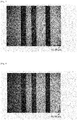
- Fig. 1 is an image from an optical stereoscopic microscope of the pattern immediately after printing.
- a mesh mark is recognizable on a surface of the pattern, and also undulations caused by sagging are recognizable at side walls.
- Fig. 2 is an image from an optical stereoscopic microscope of an electroconductive paste pattern shown in Figure 1 after drying thoroughly in the air. It can be recognized that the mesh mark has almost disappeared because the surface is smoothed in the course of drying of the paste, however the undulations at side walls become worse due to the smoothing.
- a pattern of the paste was printed on the blanket by a screen printing process, and then the pattern was transferred from the PDMS film on to a ceramic green sheet to obtain a pattern of Example 1.
- PDMS polydimethylsiloxane
- Fig. 3 is an image from an optical stereoscopic microscope of the paste pattern immediately after transfer from the PDMS film on to a ceramic green sheet. There is no recognizable mesh mark as seen in Fig. 1 , and the surface is smooth reflecting the flatness of the PDMS film. Further, the undulations at side walls due to sagging are mitigated.
- Fig. 4 is an image from an optical stereoscopic microscope of the paste shown in Fig. 3 after drying thoroughly in the air. Also, there is no recognizable sagging as seen in Fig. 1 and Fig. 2 , and it can be known that the pattern shape immediately after printing shown in Fig. 3 is maintained.
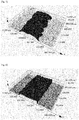
- Fig. 5 is a 3-dimensional image of a pattern obtained by observation with a confocal laser microscope of the pattern on which Fig. 2 was photographed.
- the side wall shoulder of the pattern is rounded under the influence of sagging.
- Fig. 6 is a 3-dimensional image of a pattern obtained by observation with a confocal laser microscope of the pattern on which Fig. 4 was photographed.
- a confocal laser microscope of the pattern on which Fig. 4 was photographed.
- Example 10 As a printing paste an Ag paste for a solar cell (HIMEC Type x7109, made by Namics Corporation) was used. Further, as a printing object 10A, a polyethylene terephthalate film 12 having an adhesive layer 11 on one side (SuRemLiner SRL-0753B(AS), made by Lintec Corporation). As a screen mask, a mask with a pattern containing a 9 mm-square quadrate pattern and a lead line originated from the quadrate pattern was used.
- a double side printing pattern of Example 2 was formed according to the procedures shown in Fig. 12 .
- the first paste pattern P-1 was printed thereon by a screen printing process.
- a printing object 10A was placed on the blanket 1A printed with the first pattern P-1, such that the adhesive layer 11 is positioned on the side contacting the blanket 1A.
- the second paste pattern P-2 was printed on a surface of the printing object 10A opposite to the surface facing to the blanket 1A. In this case, the pattern P-1 and the pattern P-2 were identical.
- the printing object 10A was released from the blanket 1A to transfer the first pattern P-1 to the printing object 10A, to obtain a printing object 10A of Example 2, on both sides of which paste patterns were formed.
- Fig. 13 is photographs of an obtained printing object, wherein (a) is a photograph taken from the side with an adhesive layer (marked as "Front side” in the photo (in Japanese)), and (b) is a photograph taken from the side without an adhesive layer (marked as "Back side” in the photo (in Japanese)).
- a sheet printed on both sides was obtained without requiring a step for turning a layered sheet over, so that the takt time can be reduced.
- the first and the second patterns both with accuracy sufficient for practical use, could be formed at a mutually superimposing position on the obtained sheet printed on both sides.
Landscapes
- Engineering & Computer Science (AREA)
- Power Engineering (AREA)
- Chemical & Material Sciences (AREA)
- Manufacturing & Machinery (AREA)
- Microelectronics & Electronic Packaging (AREA)
- Materials Engineering (AREA)
- Life Sciences & Earth Sciences (AREA)
- Organic Chemistry (AREA)
- Wood Science & Technology (AREA)
- Chemical Kinetics & Catalysis (AREA)
- General Chemical & Material Sciences (AREA)
- Inorganic Chemistry (AREA)
- Ceramic Engineering (AREA)
- Manufacturing Of Printed Wiring (AREA)
- Printing Methods (AREA)
- Ceramic Capacitors (AREA)
- Fixed Capacitors And Capacitor Manufacturing Machines (AREA)
- Manufacturing Of Electric Cables (AREA)
- Sustainable Development (AREA)
- Sustainable Energy (AREA)
Claims (8)
- Ausbildungsvorgang eines Musters, das dadurch gekennzeichnet ist, dass ein erstes Muster (P) auf ein Drucktuch (1A, 1B), das eine Oberfläche aufweist, die Polydimethylsiloxan umfasst, unter Verwendung einer der Folgenden gedruckt wird:
einer elektrisch leitenden Paste, einer Isolierpaste oder einer Halbleiterpaste (20) durch einen Siebdruckvorgang, und dann ein Druckobjekt (10A, 10B) auf das Drucktuch (1A, 1B) platziert wird, auf das das erste Muster (P1) gedruckt wurde, wobei ein zweites Muster (P2) zusätzlich auf eine Oberfläche des Druckobjekts (10A, 10B) gegenüber einer Oberfläche, die dem Drucktuch (1A, 1B) zugewandt ist, durch einen Siebdruckvorgang gedruckt wird, und dann das Druckobjekt (10A, 10B) von dem Drucktuch (1A, 1B) gelöst wird, um so das erste Muster (P1) auf das Druckobjekt (10A, 10B) zu übertragen. - Ausbildungsvorgang eines Musters nach Anspruch 1, wobei das Drucktuch (1A, 1B) bahnenförmig ausgebildet ist.
- Ausbildungsvorgang eines Musters nach Anspruch 1, wobei das Drucktuch (1A, 1B) rollenförmig ausgebildet ist.
- Ausbildungsvorgang eines Musters nach Anspruch 1, wobei ein Elektrodenmuster (P) unter Verwendung einer elektrisch leitenden Paste (20) ausgebildet wird.
- Ausbildungsvorgang eines Musters nach Anspruch 4, wobei das Elektrodenmuster (P) eine Verdrahtungselektrode ist, die in einem Sensorbildschirm, einer Solarzelle, einem laminierten Keramikkondensator, einer Antenne und einer Mehrlagenleiterplatte verwendet werden soll.
- Ausbildungsvorgang eines Musters nach einem der vorhergehenden Ansprüche, wobei das erste Muster (P1) und das zweite Muster (P2) Verdrahtungselektroden sind, die in einem Sensorbildschirm, einer Solarzelle, einem laminierten Keramikkondensator, einer Antenne und einer Mehrlagenleiterplatte verwendet werden sollen.
- Ausbildungsvorgang eines Musters nach Anspruch 1 bis 5, wobei der Vorgang für das Erzeugen einer kapazitätsartigen Vorrichtung verwendet wird.
- Einrichtung zum Ausbilden eines Musters, Folgendes umfassend:einen Siebdruckmechanismus,ein Drucktuch (1A, 1B) mit einer Oberfläche, die Polydimethylsiloxan umfasst; undein Druckobjekt (10A, 10B);wobei der Siebdruckmechanismus angeordnet ist, um ein erstes Muster (P) auf das Drucktuch (1A, 1B), das eine Oberfläche aufweist, die Polydimethylsiloxan umfasst, unter Verwendung einer der Folgenden zu drucken:
einer elektrisch leitenden Paste, einer Isolierpaste oder einer Halbleiterpaste (20) durch einen Siebdruckvorgang und dann durch einen Siebdruckvorgang ein zweites Muster (P2) auf eine Oberfläche des Druckobjekts (10A, 10B) gedruckt wird, wenn es auf das Drucktuch (1A, 1B) platziert wird, wobei die Oberfläche des Druckobjekts (10A, 10B), auf das das zweite Muster gedruckt wird, gegenüber einer Oberfläche ist, die dem Drucktuch (1A, 1B) zugewandt ist, und wobei das Druckobjekt (10A, 10B) von dem Drucktuch (1A, 1B) gelöst wird, um das erste Muster (P1) auf das Druckobjekt (10A, 10B) zu übertragen.
Applications Claiming Priority (2)
| Application Number | Priority Date | Filing Date | Title |
|---|---|---|---|
| JP2012210892 | 2012-09-25 | ||
| PCT/JP2013/074551 WO2014050560A1 (ja) | 2012-09-25 | 2013-09-11 | パターンの形成方法 |
Publications (3)
| Publication Number | Publication Date |
|---|---|
| EP2903007A1 EP2903007A1 (de) | 2015-08-05 |
| EP2903007A4 EP2903007A4 (de) | 2016-07-20 |
| EP2903007B1 true EP2903007B1 (de) | 2019-05-08 |
Family
ID=50387967
Family Applications (1)
| Application Number | Title | Priority Date | Filing Date |
|---|---|---|---|
| EP13840499.1A Not-in-force EP2903007B1 (de) | 2012-09-25 | 2013-09-11 | Verfahren zur herstellung eines musters |
Country Status (7)
| Country | Link |
|---|---|
| US (1) | US9697954B2 (de) |
| EP (1) | EP2903007B1 (de) |
| JP (1) | JP6080054B2 (de) |
| KR (1) | KR101759592B1 (de) |
| CN (1) | CN104685592B (de) |
| TW (1) | TWI620668B (de) |
| WO (1) | WO2014050560A1 (de) |
Families Citing this family (9)
| Publication number | Priority date | Publication date | Assignee | Title |
|---|---|---|---|---|
| JP2016219507A (ja) * | 2015-05-15 | 2016-12-22 | パナソニック株式会社 | 電子デバイスの製造方法および電子デバイス |
| JP2016219508A (ja) * | 2015-05-15 | 2016-12-22 | パナソニック株式会社 | 電子デバイスの製造方法および電子デバイス |
| JP6633488B2 (ja) * | 2015-09-29 | 2020-01-22 | 三ツ星ベルト株式会社 | 導電性ペースト及び導電膜付基板の製造方法 |
| JP6738169B2 (ja) * | 2016-03-11 | 2020-08-12 | Dowaエレクトロニクス株式会社 | 半導体光デバイスおよびその製造方法 |
| KR102007864B1 (ko) * | 2016-10-31 | 2019-08-07 | 엘에스니꼬동제련 주식회사 | 태양전지 전극용 도전성 페이스트 및 이를 사용하여 제조된 태양전지 |
| JP7100888B2 (ja) * | 2018-10-04 | 2022-07-14 | 国立研究開発法人産業技術総合研究所 | 電子部品の実装方法 |
| CN109475047B (zh) * | 2018-11-23 | 2020-12-29 | 华中科技大学 | 一种复杂曲面表面电路的制备方法及产品 |
| JP7220404B2 (ja) * | 2019-03-27 | 2023-02-10 | 島根県 | 画像中継装置および画像形成装置ならびに画像形成方法 |
| JP2021064717A (ja) * | 2019-10-15 | 2021-04-22 | 株式会社Say | 紙媒体電気回路 |
Family Cites Families (23)
| Publication number | Priority date | Publication date | Assignee | Title |
|---|---|---|---|---|
| US3535157A (en) * | 1967-12-18 | 1970-10-20 | Shipley Co | Method of coating printed circuit board having through-holes |
| JPH01220888A (ja) | 1988-02-29 | 1989-09-04 | Toshiba Corp | スクリーン印刷方法 |
| JPH085244B2 (ja) * | 1991-10-02 | 1996-01-24 | 松下電器産業株式会社 | 印刷転写法とそれに用いるオフセット印刷機 |
| US5343802A (en) * | 1991-10-02 | 1994-09-06 | Matsushita Electric Industrial Co., Ltd. | Offset printing method and offset printing machine for the same |
| US5313802A (en) * | 1993-02-16 | 1994-05-24 | Air Products And Chemicals, Inc. | Process to produce a krypton/xenon enriched stream directly from the main air distillation column |
| JP3920944B2 (ja) * | 1996-04-22 | 2007-05-30 | 大日本印刷株式会社 | パターン形成用ペーストおよびパターン形成方法 |
| GB2329866A (en) | 1997-10-01 | 1999-04-07 | Goss Graphic Systems Limited | Printing unit |
| JPH11219845A (ja) | 1998-01-30 | 1999-08-10 | Fuji Electric Co Ltd | 電極シートとその製造方法およびセラミクス電子部品の製造方法 |
| JP3603655B2 (ja) | 1999-03-25 | 2004-12-22 | 松下電器産業株式会社 | 導電性ペースト及びそれを用いたセラミック電子部品の製造方法 |
| US7943491B2 (en) * | 2004-06-04 | 2011-05-17 | The Board Of Trustees Of The University Of Illinois | Pattern transfer printing by kinetic control of adhesion to an elastomeric stamp |
| JP4665586B2 (ja) | 2005-03-31 | 2011-04-06 | 凸版印刷株式会社 | ブランケット装着機構並びにこれを利用したオフセット印刷装置及び有機el素子の製造方法 |
| KR100881182B1 (ko) * | 2006-11-21 | 2009-02-05 | 삼성전자주식회사 | 웨이퍼 사이에 형성된 디커플링 커패시터, 그 디커플링커패시터를 포함하는 웨이퍼 스택 패키지, 및 그 패키지제조 방법 |
| JP2009140790A (ja) | 2007-12-07 | 2009-06-25 | Seiko Epson Corp | 導電体およびその製造方法 |
| JP2010058330A (ja) * | 2008-09-02 | 2010-03-18 | Sharp Corp | 画像パターン形成方法および画像パターン並びに半導体デバイス、電気回路、表示体モジュール、カラーフィルタおよび発光素子 |
| JP2010250196A (ja) | 2009-04-20 | 2010-11-04 | Ricoh Co Ltd | トナー担持体の製造方法及びトナー担持体 |
| US8961835B2 (en) * | 2009-08-26 | 2015-02-24 | Lg Chem, Ltd. | Conductive metal ink composition and method for forming a conductive pattern |
| WO2011025228A2 (ko) | 2009-08-26 | 2011-03-03 | 주식회사 엘지화학 | 전도성 금속 잉크 조성물 및 전도성 패턴의 형성 방법 |
| JP5388150B2 (ja) * | 2009-08-26 | 2014-01-15 | エルジー・ケム・リミテッド | 導電性金属インク組成物および導電性パターンの形成方法 |
| KR101736462B1 (ko) | 2009-09-21 | 2017-05-16 | 한화테크윈 주식회사 | 그래핀의 제조 방법 |
| KR101077433B1 (ko) * | 2010-07-20 | 2011-10-26 | 삼성전기주식회사 | 터치스크린의 제조방법 |
| JP2012071506A (ja) | 2010-09-29 | 2012-04-12 | Toppan Printing Co Ltd | パターン形成装置及びパターン形成方法 |
| WO2012121534A2 (ko) | 2011-03-09 | 2012-09-13 | 주식회사 엘지화학 | 2 이상의 패턴화된 기판의 제조방법 및 제조장치 |
| CN102506693A (zh) | 2011-11-04 | 2012-06-20 | 南京航空航天大学 | 一种石墨烯应变测量和运动传感装置及其制法 |
-
2013
- 2013-09-11 WO PCT/JP2013/074551 patent/WO2014050560A1/ja not_active Ceased
- 2013-09-11 EP EP13840499.1A patent/EP2903007B1/de not_active Not-in-force
- 2013-09-11 US US14/430,700 patent/US9697954B2/en not_active Expired - Fee Related
- 2013-09-11 CN CN201380049763.9A patent/CN104685592B/zh not_active Expired - Fee Related
- 2013-09-11 JP JP2014538365A patent/JP6080054B2/ja active Active
- 2013-09-11 KR KR1020157009798A patent/KR101759592B1/ko not_active Expired - Fee Related
- 2013-09-25 TW TW102134537A patent/TWI620668B/zh not_active IP Right Cessation
Non-Patent Citations (1)
| Title |
|---|
| None * |
Also Published As
| Publication number | Publication date |
|---|---|
| US9697954B2 (en) | 2017-07-04 |
| KR101759592B1 (ko) | 2017-07-19 |
| WO2014050560A1 (ja) | 2014-04-03 |
| EP2903007A4 (de) | 2016-07-20 |
| JPWO2014050560A1 (ja) | 2016-08-22 |
| WO2014050560A8 (ja) | 2015-03-26 |
| EP2903007A1 (de) | 2015-08-05 |
| JP6080054B2 (ja) | 2017-02-15 |
| CN104685592A (zh) | 2015-06-03 |
| US20150243441A1 (en) | 2015-08-27 |
| TW201422447A (zh) | 2014-06-16 |
| TWI620668B (zh) | 2018-04-11 |
| CN104685592B (zh) | 2018-01-16 |
| KR20150055059A (ko) | 2015-05-20 |
Similar Documents
| Publication | Publication Date | Title |
|---|---|---|
| US9697954B2 (en) | Method for forming pattern | |
| JP4580830B2 (ja) | 画像形成方法及びそれを用いた画像形成装置 | |
| US7063014B2 (en) | Photogravure press and method for manufacturing multilayer-ceramic electronic component | |
| JP3757630B2 (ja) | 積層セラミック電子部品の製造方法 | |
| US20040209197A1 (en) | Photogravure press and method for manufacturing multilayer-ceramic electronic component | |
| JP2012114434A (ja) | 積層セラミックス電子部品の製造方法 | |
| KR20180016266A (ko) | Mlcc의 효율을 높이는 제조 방법 및 그에 따른 mlcc | |
| CN112918077B (zh) | 凹版印刷版和使用该凹版印刷版的凹版印刷装置 | |
| JP2014128924A (ja) | グラビアオフセット印刷方法 | |
| JP2002141245A (ja) | セラミック電子部品の製造方法および装置 | |
| JPH03108307A (ja) | セラミック電子部品の製造方法 | |
| CN114885508A (zh) | 柔性集成电路生产系统和方法 | |
| JP6079232B2 (ja) | グラビアオフセット印刷方法 | |
| JP7491055B2 (ja) | グラビア印刷方法、グラビア印刷機、および積層セラミック電子部品の製造方法 | |
| JPH09237737A (ja) | 積層セラミックコンデンサの製造方法 | |
| CN217258988U (zh) | 凹版及凹版印刷机 | |
| JP6047895B2 (ja) | グラビアオフセット印刷用ブランケット、及び、それを用いた印刷配線基材の製造方法 | |
| JPH09162066A (ja) | 積層セラミック電子部品の製造方法及びその製造装置 | |
| JP3114563B2 (ja) | 積層電子部品の製造方法 | |
| JP4126903B2 (ja) | 積層セラミック電子部品の製造装置および製造方法 | |
| JP2007220879A (ja) | セラミックデバイスの製造方法 | |
| TW201446536A (zh) | 多工位柔版印刷方法及系統 | |
| JPH0136996B2 (de) | ||
| JP2005183433A (ja) | 積層体の製造方法 | |
| JPH03206A (ja) | セラミック生シートの製造方法 |
Legal Events
| Date | Code | Title | Description |
|---|---|---|---|
| PUAI | Public reference made under article 153(3) epc to a published international application that has entered the european phase |
Free format text: ORIGINAL CODE: 0009012 |
|
| 17P | Request for examination filed |
Effective date: 20150320 |
|
| AK | Designated contracting states |
Kind code of ref document: A1 Designated state(s): AL AT BE BG CH CY CZ DE DK EE ES FI FR GB GR HR HU IE IS IT LI LT LU LV MC MK MT NL NO PL PT RO RS SE SI SK SM TR |
|
| AX | Request for extension of the european patent |
Extension state: BA ME |
|
| RIN1 | Information on inventor provided before grant (corrected) |
Inventor name: NOMURA, KENICHI Inventor name: YOSHIDA, MANABU Inventor name: USHIJIMA, HIROBUMI Inventor name: IWASE, NORIKO |
|
| DAX | Request for extension of the european patent (deleted) | ||
| RIN1 | Information on inventor provided before grant (corrected) |
Inventor name: USHIJIMA, HIROBUMI Inventor name: NOMURA, KENICHI Inventor name: IWASE, NORIKO Inventor name: YOSHIDA, MANABU |
|
| RA4 | Supplementary search report drawn up and despatched (corrected) |
Effective date: 20160621 |
|
| RIC1 | Information provided on ipc code assigned before grant |
Ipc: C09D 11/00 20140101ALI20160615BHEP Ipc: H01G 4/30 20060101ALI20160615BHEP Ipc: H01G 4/12 20060101ALI20160615BHEP Ipc: H05K 3/20 20060101ALI20160615BHEP Ipc: H01G 13/00 20130101ALI20160615BHEP Ipc: H01B 13/00 20060101AFI20160615BHEP |
|
| STAA | Information on the status of an ep patent application or granted ep patent |
Free format text: STATUS: EXAMINATION IS IN PROGRESS |
|
| 17Q | First examination report despatched |
Effective date: 20180625 |
|
| GRAP | Despatch of communication of intention to grant a patent |
Free format text: ORIGINAL CODE: EPIDOSNIGR1 |
|
| STAA | Information on the status of an ep patent application or granted ep patent |
Free format text: STATUS: GRANT OF PATENT IS INTENDED |
|
| INTG | Intention to grant announced |
Effective date: 20181206 |
|
| GRAS | Grant fee paid |
Free format text: ORIGINAL CODE: EPIDOSNIGR3 |
|
| GRAA | (expected) grant |
Free format text: ORIGINAL CODE: 0009210 |
|
| STAA | Information on the status of an ep patent application or granted ep patent |
Free format text: STATUS: THE PATENT HAS BEEN GRANTED |
|
| AK | Designated contracting states |
Kind code of ref document: B1 Designated state(s): AL AT BE BG CH CY CZ DE DK EE ES FI FR GB GR HR HU IE IS IT LI LT LU LV MC MK MT NL NO PL PT RO RS SE SI SK SM TR |
|
| REG | Reference to a national code |
Ref country code: GB Ref legal event code: FG4D |
|
| REG | Reference to a national code |
Ref country code: CH Ref legal event code: EP Ref country code: AT Ref legal event code: REF Ref document number: 1131492 Country of ref document: AT Kind code of ref document: T Effective date: 20190515 |
|
| REG | Reference to a national code |
Ref country code: DE Ref legal event code: R096 Ref document number: 602013055212 Country of ref document: DE Ref country code: IE Ref legal event code: FG4D |
|
| REG | Reference to a national code |
Ref country code: NL Ref legal event code: MP Effective date: 20190508 |
|
| REG | Reference to a national code |
Ref country code: LT Ref legal event code: MG4D |
|
| PG25 | Lapsed in a contracting state [announced via postgrant information from national office to epo] |
Ref country code: NL Free format text: LAPSE BECAUSE OF FAILURE TO SUBMIT A TRANSLATION OF THE DESCRIPTION OR TO PAY THE FEE WITHIN THE PRESCRIBED TIME-LIMIT Effective date: 20190508 Ref country code: SE Free format text: LAPSE BECAUSE OF FAILURE TO SUBMIT A TRANSLATION OF THE DESCRIPTION OR TO PAY THE FEE WITHIN THE PRESCRIBED TIME-LIMIT Effective date: 20190508 Ref country code: HR Free format text: LAPSE BECAUSE OF FAILURE TO SUBMIT A TRANSLATION OF THE DESCRIPTION OR TO PAY THE FEE WITHIN THE PRESCRIBED TIME-LIMIT Effective date: 20190508 Ref country code: ES Free format text: LAPSE BECAUSE OF FAILURE TO SUBMIT A TRANSLATION OF THE DESCRIPTION OR TO PAY THE FEE WITHIN THE PRESCRIBED TIME-LIMIT Effective date: 20190508 Ref country code: LT Free format text: LAPSE BECAUSE OF FAILURE TO SUBMIT A TRANSLATION OF THE DESCRIPTION OR TO PAY THE FEE WITHIN THE PRESCRIBED TIME-LIMIT Effective date: 20190508 Ref country code: AL Free format text: LAPSE BECAUSE OF FAILURE TO SUBMIT A TRANSLATION OF THE DESCRIPTION OR TO PAY THE FEE WITHIN THE PRESCRIBED TIME-LIMIT Effective date: 20190508 Ref country code: NO Free format text: LAPSE BECAUSE OF FAILURE TO SUBMIT A TRANSLATION OF THE DESCRIPTION OR TO PAY THE FEE WITHIN THE PRESCRIBED TIME-LIMIT Effective date: 20190808 Ref country code: PT Free format text: LAPSE BECAUSE OF FAILURE TO SUBMIT A TRANSLATION OF THE DESCRIPTION OR TO PAY THE FEE WITHIN THE PRESCRIBED TIME-LIMIT Effective date: 20190908 Ref country code: FI Free format text: LAPSE BECAUSE OF FAILURE TO SUBMIT A TRANSLATION OF THE DESCRIPTION OR TO PAY THE FEE WITHIN THE PRESCRIBED TIME-LIMIT Effective date: 20190508 |
|
| PG25 | Lapsed in a contracting state [announced via postgrant information from national office to epo] |
Ref country code: BG Free format text: LAPSE BECAUSE OF FAILURE TO SUBMIT A TRANSLATION OF THE DESCRIPTION OR TO PAY THE FEE WITHIN THE PRESCRIBED TIME-LIMIT Effective date: 20190808 Ref country code: LV Free format text: LAPSE BECAUSE OF FAILURE TO SUBMIT A TRANSLATION OF THE DESCRIPTION OR TO PAY THE FEE WITHIN THE PRESCRIBED TIME-LIMIT Effective date: 20190508 Ref country code: GR Free format text: LAPSE BECAUSE OF FAILURE TO SUBMIT A TRANSLATION OF THE DESCRIPTION OR TO PAY THE FEE WITHIN THE PRESCRIBED TIME-LIMIT Effective date: 20190809 Ref country code: RS Free format text: LAPSE BECAUSE OF FAILURE TO SUBMIT A TRANSLATION OF THE DESCRIPTION OR TO PAY THE FEE WITHIN THE PRESCRIBED TIME-LIMIT Effective date: 20190508 |
|
| REG | Reference to a national code |
Ref country code: AT Ref legal event code: MK05 Ref document number: 1131492 Country of ref document: AT Kind code of ref document: T Effective date: 20190508 |
|
| PG25 | Lapsed in a contracting state [announced via postgrant information from national office to epo] |
Ref country code: EE Free format text: LAPSE BECAUSE OF FAILURE TO SUBMIT A TRANSLATION OF THE DESCRIPTION OR TO PAY THE FEE WITHIN THE PRESCRIBED TIME-LIMIT Effective date: 20190508 Ref country code: SK Free format text: LAPSE BECAUSE OF FAILURE TO SUBMIT A TRANSLATION OF THE DESCRIPTION OR TO PAY THE FEE WITHIN THE PRESCRIBED TIME-LIMIT Effective date: 20190508 Ref country code: CZ Free format text: LAPSE BECAUSE OF FAILURE TO SUBMIT A TRANSLATION OF THE DESCRIPTION OR TO PAY THE FEE WITHIN THE PRESCRIBED TIME-LIMIT Effective date: 20190508 Ref country code: RO Free format text: LAPSE BECAUSE OF FAILURE TO SUBMIT A TRANSLATION OF THE DESCRIPTION OR TO PAY THE FEE WITHIN THE PRESCRIBED TIME-LIMIT Effective date: 20190508 Ref country code: AT Free format text: LAPSE BECAUSE OF FAILURE TO SUBMIT A TRANSLATION OF THE DESCRIPTION OR TO PAY THE FEE WITHIN THE PRESCRIBED TIME-LIMIT Effective date: 20190508 Ref country code: DK Free format text: LAPSE BECAUSE OF FAILURE TO SUBMIT A TRANSLATION OF THE DESCRIPTION OR TO PAY THE FEE WITHIN THE PRESCRIBED TIME-LIMIT Effective date: 20190508 |
|
| REG | Reference to a national code |
Ref country code: DE Ref legal event code: R097 Ref document number: 602013055212 Country of ref document: DE |
|
| PG25 | Lapsed in a contracting state [announced via postgrant information from national office to epo] |
Ref country code: SM Free format text: LAPSE BECAUSE OF FAILURE TO SUBMIT A TRANSLATION OF THE DESCRIPTION OR TO PAY THE FEE WITHIN THE PRESCRIBED TIME-LIMIT Effective date: 20190508 Ref country code: IT Free format text: LAPSE BECAUSE OF FAILURE TO SUBMIT A TRANSLATION OF THE DESCRIPTION OR TO PAY THE FEE WITHIN THE PRESCRIBED TIME-LIMIT Effective date: 20190508 |
|
| PLBE | No opposition filed within time limit |
Free format text: ORIGINAL CODE: 0009261 |
|
| STAA | Information on the status of an ep patent application or granted ep patent |
Free format text: STATUS: NO OPPOSITION FILED WITHIN TIME LIMIT |
|
| PG25 | Lapsed in a contracting state [announced via postgrant information from national office to epo] |
Ref country code: TR Free format text: LAPSE BECAUSE OF FAILURE TO SUBMIT A TRANSLATION OF THE DESCRIPTION OR TO PAY THE FEE WITHIN THE PRESCRIBED TIME-LIMIT Effective date: 20190508 |
|
| 26N | No opposition filed |
Effective date: 20200211 |
|
| PG25 | Lapsed in a contracting state [announced via postgrant information from national office to epo] |
Ref country code: PL Free format text: LAPSE BECAUSE OF FAILURE TO SUBMIT A TRANSLATION OF THE DESCRIPTION OR TO PAY THE FEE WITHIN THE PRESCRIBED TIME-LIMIT Effective date: 20190508 |
|
| PG25 | Lapsed in a contracting state [announced via postgrant information from national office to epo] |
Ref country code: MC Free format text: LAPSE BECAUSE OF FAILURE TO SUBMIT A TRANSLATION OF THE DESCRIPTION OR TO PAY THE FEE WITHIN THE PRESCRIBED TIME-LIMIT Effective date: 20190508 Ref country code: SI Free format text: LAPSE BECAUSE OF FAILURE TO SUBMIT A TRANSLATION OF THE DESCRIPTION OR TO PAY THE FEE WITHIN THE PRESCRIBED TIME-LIMIT Effective date: 20190508 |
|
| REG | Reference to a national code |
Ref country code: CH Ref legal event code: PL |
|
| PG25 | Lapsed in a contracting state [announced via postgrant information from national office to epo] |
Ref country code: LU Free format text: LAPSE BECAUSE OF NON-PAYMENT OF DUE FEES Effective date: 20190911 Ref country code: IE Free format text: LAPSE BECAUSE OF NON-PAYMENT OF DUE FEES Effective date: 20190911 Ref country code: LI Free format text: LAPSE BECAUSE OF NON-PAYMENT OF DUE FEES Effective date: 20190930 Ref country code: CH Free format text: LAPSE BECAUSE OF NON-PAYMENT OF DUE FEES Effective date: 20190930 |
|
| REG | Reference to a national code |
Ref country code: BE Ref legal event code: MM Effective date: 20190930 |
|
| PG25 | Lapsed in a contracting state [announced via postgrant information from national office to epo] |
Ref country code: BE Free format text: LAPSE BECAUSE OF NON-PAYMENT OF DUE FEES Effective date: 20190930 |
|
| GBPC | Gb: european patent ceased through non-payment of renewal fee |
Effective date: 20190911 |
|
| PG25 | Lapsed in a contracting state [announced via postgrant information from national office to epo] |
Ref country code: GB Free format text: LAPSE BECAUSE OF NON-PAYMENT OF DUE FEES Effective date: 20190911 Ref country code: FR Free format text: LAPSE BECAUSE OF NON-PAYMENT OF DUE FEES Effective date: 20190930 |
|
| PG25 | Lapsed in a contracting state [announced via postgrant information from national office to epo] |
Ref country code: CY Free format text: LAPSE BECAUSE OF FAILURE TO SUBMIT A TRANSLATION OF THE DESCRIPTION OR TO PAY THE FEE WITHIN THE PRESCRIBED TIME-LIMIT Effective date: 20190508 |
|
| PG25 | Lapsed in a contracting state [announced via postgrant information from national office to epo] |
Ref country code: IS Free format text: LAPSE BECAUSE OF FAILURE TO SUBMIT A TRANSLATION OF THE DESCRIPTION OR TO PAY THE FEE WITHIN THE PRESCRIBED TIME-LIMIT Effective date: 20190908 |
|
| PG25 | Lapsed in a contracting state [announced via postgrant information from national office to epo] |
Ref country code: HU Free format text: LAPSE BECAUSE OF FAILURE TO SUBMIT A TRANSLATION OF THE DESCRIPTION OR TO PAY THE FEE WITHIN THE PRESCRIBED TIME-LIMIT; INVALID AB INITIO Effective date: 20130911 Ref country code: MT Free format text: LAPSE BECAUSE OF FAILURE TO SUBMIT A TRANSLATION OF THE DESCRIPTION OR TO PAY THE FEE WITHIN THE PRESCRIBED TIME-LIMIT Effective date: 20190508 |
|
| PGFP | Annual fee paid to national office [announced via postgrant information from national office to epo] |
Ref country code: DE Payment date: 20210720 Year of fee payment: 9 |
|
| PG25 | Lapsed in a contracting state [announced via postgrant information from national office to epo] |
Ref country code: MK Free format text: LAPSE BECAUSE OF FAILURE TO SUBMIT A TRANSLATION OF THE DESCRIPTION OR TO PAY THE FEE WITHIN THE PRESCRIBED TIME-LIMIT Effective date: 20190508 |
|
| REG | Reference to a national code |
Ref country code: DE Ref legal event code: R119 Ref document number: 602013055212 Country of ref document: DE |
|
| PG25 | Lapsed in a contracting state [announced via postgrant information from national office to epo] |
Ref country code: DE Free format text: LAPSE BECAUSE OF NON-PAYMENT OF DUE FEES Effective date: 20230401 |