EP2903157A1 - Dispositif amplificateur hyperfréquence - Google Patents
Dispositif amplificateur hyperfréquence Download PDFInfo
- Publication number
- EP2903157A1 EP2903157A1 EP13840282.1A EP13840282A EP2903157A1 EP 2903157 A1 EP2903157 A1 EP 2903157A1 EP 13840282 A EP13840282 A EP 13840282A EP 2903157 A1 EP2903157 A1 EP 2903157A1
- Authority
- EP
- European Patent Office
- Prior art keywords
- frequency
- microwave amplifier
- amplifier
- line
- microwave
- Prior art date
- Legal status (The legal status is an assumption and is not a legal conclusion. Google has not performed a legal analysis and makes no representation as to the accuracy of the status listed.)
- Granted
Links
Images

Classifications
-
- H—ELECTRICITY
- H03—ELECTRONIC CIRCUITRY
- H03F—AMPLIFIERS
- H03F1/00—Details of amplifiers with only discharge tubes, only semiconductor devices or only unspecified devices as amplifying elements
- H03F1/02—Modifications of amplifiers to raise the efficiency, e.g. gliding Class A stages, use of an auxiliary oscillation
- H03F1/0205—Modifications of amplifiers to raise the efficiency, e.g. gliding Class A stages, use of an auxiliary oscillation in transistor amplifiers
-
- H—ELECTRICITY
- H03—ELECTRONIC CIRCUITRY
- H03F—AMPLIFIERS
- H03F1/00—Details of amplifiers with only discharge tubes, only semiconductor devices or only unspecified devices as amplifying elements
- H03F1/32—Modifications of amplifiers to reduce non-linear distortion
- H03F1/3205—Modifications of amplifiers to reduce non-linear distortion in field-effect transistor amplifiers
-
- H—ELECTRICITY
- H03—ELECTRONIC CIRCUITRY
- H03F—AMPLIFIERS
- H03F3/00—Amplifiers with only discharge tubes or only semiconductor devices as amplifying elements
- H03F3/189—High-frequency amplifiers, e.g. radio frequency amplifiers
- H03F3/19—High-frequency amplifiers, e.g. radio frequency amplifiers with semiconductor devices only
-
- H—ELECTRICITY
- H03—ELECTRONIC CIRCUITRY
- H03F—AMPLIFIERS
- H03F3/00—Amplifiers with only discharge tubes or only semiconductor devices as amplifying elements
- H03F3/20—Power amplifiers, e.g. Class B amplifiers, Class C amplifiers
- H03F3/24—Power amplifiers, e.g. Class B amplifiers, Class C amplifiers of transmitter output stages
- H03F3/245—Power amplifiers, e.g. Class B amplifiers, Class C amplifiers of transmitter output stages with semiconductor devices only
-
- H—ELECTRICITY
- H03—ELECTRONIC CIRCUITRY
- H03F—AMPLIFIERS
- H03F3/00—Amplifiers with only discharge tubes or only semiconductor devices as amplifying elements
- H03F3/60—Amplifiers in which coupling networks have distributed constants, e.g. with waveguide resonators
- H03F3/601—Amplifiers in which coupling networks have distributed constants, e.g. with waveguide resonators using FET's, e.g. GaAs FET's
-
- H—ELECTRICITY
- H03—ELECTRONIC CIRCUITRY
- H03F—AMPLIFIERS
- H03F2200/00—Indexing scheme relating to amplifiers
- H03F2200/108—A coil being added in the drain circuit of a FET amplifier stage, e.g. for noise reducing purposes
-
- H—ELECTRICITY
- H03—ELECTRONIC CIRCUITRY
- H03F—AMPLIFIERS
- H03F2200/00—Indexing scheme relating to amplifiers
- H03F2200/12—A bias circuit for some stages being shown using transmission lines
-
- H—ELECTRICITY
- H03—ELECTRONIC CIRCUITRY
- H03F—AMPLIFIERS
- H03F2200/00—Indexing scheme relating to amplifiers
- H03F2200/267—A capacitor based passive circuit, e.g. filter, being used in an amplifying circuit
-
- H—ELECTRICITY
- H03—ELECTRONIC CIRCUITRY
- H03F—AMPLIFIERS
- H03F2200/00—Indexing scheme relating to amplifiers
- H03F2200/391—Indexing scheme relating to amplifiers the output circuit of an amplifying stage comprising an LC-network
-
- H—ELECTRICITY
- H03—ELECTRONIC CIRCUITRY
- H03F—AMPLIFIERS
- H03F2200/00—Indexing scheme relating to amplifiers
- H03F2200/555—A voltage generating circuit being realised for biasing different circuit elements
Definitions
- the present invention relates to a microwave amplifier used in high-frequency bands such as microwave and millimetric wave bands using an active element.
- the present invention further relates to a microwave amplifier in which a plurality of communication carriers having different frequencies is simultaneously input.
- microwave amplifiers used in communication-related applications, there are instances in which a plurality of communication carriers having different frequencies in a fixed operating band is input simultaneously. However, for microwave amplifiers, mutual interaction may occur between a plurality of communication carriers due to the generation of a beat signal between the plurality of communication carriers with different frequencies.
- Patent Literature 1 proposes a microwave amplifier which has a good distortion characteristic even when many communication carrier frequencies are included in a microwave signal configured to be amplified.
- a filter circuit which becomes a high impedance with the communication carrier frequency of a microwave signal and becomes a low impedance with the frequency of a beat signal that is generated from a plurality of communication carrier frequencies is connected to a drain of a field effect transistor (FET).
- FET field effect transistor
- a capacitor which short-circuits a beat signal is connected between the other end and a ground (GND).
- Patent Literature 2 discloses about reducing significantly the gain in low frequency bands which causes a problem when amplifying a plurality of communication carriers of a microwave amplifier, and reducing low frequency components on the input and output side of an amplifier.
- ends of bias supply lines having predetermined lengths are connected to a connecting point of a microwave amplifier circuit having a semiconductor element and an input side transmission line, and to a connecting point of the microwave amplifier circuit and an output side transmission line respectively.
- Capacitors are connected to other ends of the bias supply lines, respectively.
- a parallel circuit consisting of a resistor and a capacitor is loaded between the connecting point of the input side bias circuit to the input side transmission line and the input terminal of the microwave amplifier circuit.
- the ultra-high frequency semiconductor circuit is configured to be provided with a capacitor in parallel with a resistor in a bias circuit, the capacitor having a sufficiently small reactance at an ultra-high frequency in the vicinity of the necessary frequency and having a large reactance at a low frequency.
- the microwave amplifier in Patent Literature 1 uses an LC resonant circuit and suppresses mutual interaction between a plurality of communication carriers by lowering the impedance observed from the amplifier in a frequency of a beat signal that is generated between a plurality of frequencies.
- Patent Literature 2 is to suppress gain in response to an input signal of a low frequency region which is not a remedy for addressing performance degradation including gain drops and increases in the amount of distortion due to mutual influence between communication carriers.
- Patent Literature 2 moreover, has a drawback of increasing consumption of direct current power because a resistor is added in series in the power source supply circuit.
- the ultra-high frequency semiconductor circuit in Patent Literature 3 can prevent unstable operations such as oscillation of the amplifier due to external disturbances (noise and the like), feedback, and the like because gain of the ultra-high frequency semiconductor circuit can be reduced in a low frequency at which gain of a field effect transistor (FET) itself is high.
- FET field effect transistor
- the invention has been made in order to solve the aforementioned type of problems, and thus the object of the invention is to suppress extreme performance degradation caused by frequency relationship of a specific beat signal even when a plurality of communication carriers is input in a wideband.
- the microwave amplifier set forth in view of the present invention is a microwave amplifier for amplifying a microwave signal using an active element, that includes a bias circuit that includes a line having an electrical length of one quarter the wavelength at the frequency configured to be amplified by the microwave amplifier and being connected between the output terminal of the active element and a bias voltage source, and a first capacitor element connected between a terminal where the line is connected to the bias voltage source and a ground that defines a reference potential of the microwave amplifier; and a resonant circuit that includes a resistor and a second capacitor element, the resistor and the second capacitor element connected in series between the ground and the terminal where the line is connected to the bias voltage source.
- FIG. 1 is a circuit diagram of a microwave amplifier according to Embodiment 1 of the present invention.
- a line 20 having an electrical length ⁇ g/4 that is one quarter of the wavelength at a frequency ⁇ g configured to be amplified by the microwave amplifier is connected between an output terminal of an amplifier 11, which is an active element, and a bias voltage source 13.
- FET field effect transistor
- a capacitor 14 (first capacitor element) is connected between the terminal where the line 20 is connected to the bias voltage source 13 and a ground 10 that defines the reference potential of the microwave amplifier. Moreover, a resistor 15 and a capacitor 16 (second capacitor element) are connected in series between the ground 10 and the terminal where the line 20 is connected to the bias voltage source 13.
- FIG. 2 is a circuit diagram of a microwave amplifier that includes a conventional bias circuit.
- the microwave amplifier is configured with an amplifier output port 12 that extracts frequencies of communication carriers and a port that connects the bias voltage source 13 in order to supply DC power on the output part of the amplifier 11 configured with an active element.
- the line 20 having a line length ⁇ g/4 that depends on a wavelength ⁇ g of communication carriers taking into consideration a wavelength shortening rate on a printed circuit board, is connected between the amplifier 11 and the bias voltage source 13. And at an end of the line 20, it is disposed a bias circuit that includes the capacitor 14, used to short-circuit communication band signals, for forming a short-circuit point at communication carrier frequencies.
- FIG. 3 is a diagram showing mutual interaction that is caused by two waves in a communication band.
- the magnitude of power of an input wave and an output wave of the amplifier 11 each are expressed as ratios to a signal power of frequency ⁇ 1.
- the power of a communication carrier 1 of frequency ⁇ 1 and the power of a communication carrier 2 of frequency ⁇ 2 are power P1 [W] and P2 [W] respectively.
- Power P1 [W] of the communication carrier 1 is amplified by the gain G of the amplifier 11 to power G x P1 [W].
- the amplifier 11 Assuming that the amplifier 11 is provided with linear gain in a frequency range including frequency ⁇ 1 and frequency ⁇ 2 and also assuming that the amplifier 11 has the same gain G at the frequency ⁇ 2 of the communication carrier 2, then the power of the output wave of the communication carrier 2 would normally become G x P2 [W] which corresponds to the total length of the solid arrow and a dotted arrow 4 directly above the solid arrow shown on the right portion of FIG. 3 .
- a beat signal 3 having a frequency of ( ⁇ 2- ⁇ 1) is generated due to the communication carrier 1 ( ⁇ 1) and the communication carrier 2 ( ⁇ 2).
- the impedance (R + jX) (j: imaginary unit) of the output side observed from the amplifier 11 at a frequency of a beat signal 3 ( ⁇ 2 - ⁇ 1) is a finite value. Therefore a voltage fluctuation ⁇ Vb in proportion to power Pb of beat signal 3 is generated on the output side of the amplifier 11.
- ⁇ VB Pb ⁇ R + jX 1 / 2
- the mixing of communication carrier 1 and the beat signal 3 causes the drop of applied voltage to the communication carrier 2 and the drop of the gain for the communication carrier 2 as well.
- the amount of the gain drop is dependent on followings.
- the microwave amplifier according to Embodiment 1 includes a series circuit of the resistor 15 and the capacitor 16 connected where capacitor 14 is connected.
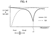
- FIG. 4 is a diagram showing a characteristic example of a second capacitor element utilized by the microwave amplifier according to Embodiment 1.
- the capacitance of the capacitor 14 is set to short-circuit signals in communication band, therefore the capacitor 14 can be considered to be zero ⁇ (short-circuited) at the frequency configured to be amplified. Accordingly, the circuit on the bias voltage source 13 side cannot be observed from the connection point of the line 20 having a one quarter wavelength and the capacitor 14.
- the impedance on the bias voltage source 13 side as observed from the connection point of the line 20 and a main line (output side of the amplifier 11) can be considered to be infinite, output loss in the necessary frequency is not generated.
- the capacitance of the capacitor 14 is "C1"
- the impedance in response to frequency f 1 in a communication band corresponds to the absolute value of 1/(j2 ⁇ f 1 x C 1 ) with "j" being the imaginary unit, and generally, the capacitance value of the capacitor is set so that the impedance value is lower than or equal to 1 ⁇ .
- the capacitor 14 is for short-circuiting signals in communication band, at the frequency of the beat signal, the impedance becomes a finite value and the circuit on the bias voltage source 13 side become being observed from the connection point of the line 20 that has a one quarter wavelength and the capacitor 14.
- the impedance equal to 1/(j2 ⁇ f x C) capacitance "C" at a frequency "f", as for the impedance by the capacitor 14, when the frequency "f 2 " of a beat signal becomes smaller compared with a communication band then the impedance also becomes larger proportion to the value of (f 1 /f 2 ).
- the impedance on the side of the bias voltage source 13 as observed from the connection point of the line 20 that has a one quarter wavelength and the main line (output side of the amplifier 11) becomes the combined impedance of the inductance of the line 20, the resistance of the resistor 15, and the capacitance of the capacitors 14 and 16.
- the inductance of the line 20, the resistor 15, and the capacitor 16 constitute the resonant circuit.
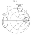
- FIG. 5 is a diagram showing impedance observed from an active element in frequency regions of a beat signal.
- Regions 18 indicate the range of impedance of the resonant circuit without the resistor 15.
- Region 19 indicates the range of impedance of the resonant circuit with the resistor 15.
- the impedance observed from the amplifier 11 can be recognized as the impedance grouped in the region 19 of the vicinity of the real axis while avoiding the regions 18 (totally reflected or in the vicinity) shown in FIG. 5 with respect to a frequency of any beat signal generated by the frequencies of a plurality of communication carriers.
- the region 19 is the vicinity of the real axis located inside the circumference of the Smith chart.
- the effect of the gain drop of communication carrier 2 caused by the beat signal 3, as shown in FIG. 3 is influenced by impedance (R + jX) [ ⁇ ] on the load side as observed from the amplifier 11 at a frequency of the beat signal 3 ( ⁇ 2 - ⁇ 1).
- the Smith chart in FIG. 5 shows that the impedance observed from a field effect transistor (FET) in the region of the frequency of the beat signal 3 is positioned inside the circumference of the Smith chart due to the resistor 15.
- FET field effect transistor
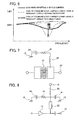
- FIG. 6 is a diagram showing the variation in gain of a communication carrier due to the presence/absence of resistance in a resonant circuit when a plurality of communication carriers is input.
- the adding of resistance components to the resonant circuit which brings an effect of lowering the "Q" value of the resonant circuit, suppresses mutual interaction between communication carriers even when a plurality of communication carriers, each of which has an arbitrary frequency in a wideband, is input. This makes stable operation possible without being influenced by the number of input communication carriers or the frequency relationship between communication carriers.
- Patent Literature 2 an effect that contributes towards stable operation can be expected when various components and the choice for placing the elements are properly selected.
- Embodiment 1 because no resistance components are inserted on a path through which direct current flows, there is an additional advantage of being capable of performing stable operation while maintaining high efficiency performance of the amplifier itself.
- FIG. 7 is a circuit diagram of a microwave amplifier according to Embodiment 2 of the present invention.
- the microwave amplifier in Embodiment 2 includes an inductor 23, a capacitor 24, and a resistor 25 connected in series between the output side of an amplifier 21 and the ground 10.
- the amplifier 21 includes an active element.
- the amplifier 21 transmits power at communication carrier frequencies and direct-current power is supplied to an amplifier output port 22.
- the inductor 23, the resistor 25 and the capacitor 24 in Embodiment 2 are in a configuration in which, in place of the line 20 of Embodiment 1, the inductor 23 corresponding to the inductance of the line 20 is disposed for the frequency of the beat signal 3.
- the impedance at a frequency of the beat signal 3 as observed from the amplifier 21 can be disposed within the region 19 in the vicinity of the real axis on the Smith chart, in the same manner as Embodiment 1, while minimizing loss of power in communication carrier frequencies and loss of DC power at the output part of the amplifier 21. Hence a condition can be avoided in which a mutual interaction between a plurality of communication carriers becomes extremely large.
- FIG. 8 is a circuit diagram of a microwave amplifier according to Embodiment 3 of the present invention.
- an inductor 36 is added in between the bias circuit and the bias voltage source 13.
- the inductor 36 passes direct current and low-frequency range signals while blocking signals with higher frequencies.
- the inductor 36 suppresses the influence of impedance of the power source circuit on impedance observed on the side of the bias voltage source 13 from the amplifier 11.
- the impedance value at the frequency of the beat signal 3 is determined by the resistor 15 and the capacitor 16.
- the microwave amplifier in Embodiment 3, in addition to the effects described in Embodiment 1, the microwave amplifier can also suppress the influences of impedance of the power source circuit.
Landscapes
- Engineering & Computer Science (AREA)
- Power Engineering (AREA)
- Physics & Mathematics (AREA)
- Nonlinear Science (AREA)
- Amplifiers (AREA)
- Microwave Amplifiers (AREA)
Applications Claiming Priority (2)
| Application Number | Priority Date | Filing Date | Title |
|---|---|---|---|
| JP2012210863A JP6112500B2 (ja) | 2012-09-25 | 2012-09-25 | マイクロ波増幅器 |
| PCT/JP2013/074857 WO2014050611A1 (fr) | 2012-09-25 | 2013-09-13 | Dispositif amplificateur hyperfréquence |
Publications (3)
| Publication Number | Publication Date |
|---|---|
| EP2903157A1 true EP2903157A1 (fr) | 2015-08-05 |
| EP2903157A4 EP2903157A4 (fr) | 2016-05-18 |
| EP2903157B1 EP2903157B1 (fr) | 2019-01-09 |
Family
ID=50388018
Family Applications (1)
| Application Number | Title | Priority Date | Filing Date |
|---|---|---|---|
| EP13840282.1A Active EP2903157B1 (fr) | 2012-09-25 | 2013-09-13 | Dispositif amplificateur hyperfréquence |
Country Status (11)
| Country | Link |
|---|---|
| US (1) | US9543898B2 (fr) |
| EP (1) | EP2903157B1 (fr) |
| JP (1) | JP6112500B2 (fr) |
| CN (1) | CN104662795B (fr) |
| BR (1) | BR112015006526A2 (fr) |
| CA (1) | CA2885911A1 (fr) |
| DK (1) | DK2903157T3 (fr) |
| ES (1) | ES2710751T3 (fr) |
| PH (1) | PH12015500606A1 (fr) |
| SG (1) | SG11201502097WA (fr) |
| WO (1) | WO2014050611A1 (fr) |
Cited By (1)
| Publication number | Priority date | Publication date | Assignee | Title |
|---|---|---|---|---|
| RU167770U1 (ru) * | 2016-05-24 | 2017-01-10 | Акционерное общество "Научно-производственное предприятие "Исток" имени А.И. Шокина" (АО "НПП "Исток" им. Шокина") | Балансный усилитель СВЧ |
Families Citing this family (4)
| Publication number | Priority date | Publication date | Assignee | Title |
|---|---|---|---|---|
| CN111510074B (zh) * | 2019-01-31 | 2023-06-23 | 苏州远创达科技有限公司 | 一种高视频带宽的射频功率放大器 |
| JP7258612B2 (ja) * | 2019-03-15 | 2023-04-17 | 株式会社東芝 | 高周波回路 |
| CN110113015B (zh) * | 2019-04-29 | 2023-03-24 | 中国电子科技集团公司第十三研究所 | 栅极偏置电路及功率放大器 |
| KR102756602B1 (ko) | 2019-09-17 | 2025-01-21 | 한국전자통신연구원 | 초고주파 증폭 회로 |
Family Cites Families (17)
| Publication number | Priority date | Publication date | Assignee | Title |
|---|---|---|---|---|
| JPS62209909A (ja) | 1986-03-11 | 1987-09-16 | Mitsubishi Electric Corp | 超高周波半導体回路 |
| JPH01233812A (ja) * | 1988-03-14 | 1989-09-19 | Fujitsu Ltd | マイクロ波用多段増幅回路 |
| JPH0983269A (ja) * | 1995-09-20 | 1997-03-28 | Fujitsu Ltd | バイアス回路 |
| JPH1141042A (ja) | 1997-07-17 | 1999-02-12 | Mitsubishi Electric Corp | マイクロ波増幅器 |
| JP3123484B2 (ja) | 1997-10-29 | 2001-01-09 | 日本電気株式会社 | マイクロ波増幅器 |
| JPH11234063A (ja) * | 1998-02-10 | 1999-08-27 | Fujitsu Ltd | 高周波用増幅器 |
| US6124767A (en) * | 1998-05-21 | 2000-09-26 | Delphi Components, Inc. | RF/Microwave oscillator |
| US6166599A (en) * | 1998-12-04 | 2000-12-26 | Qualcomm, Inc. | Impedance matching networks for non-linear circuits |
| CN1315074A (zh) | 1999-06-30 | 2001-09-26 | 三菱电机株式会社 | 微波放大器 |
| US6509799B1 (en) | 2000-11-09 | 2003-01-21 | Intel Corporation | Electrically tuned integrated amplifier for wireless communications |
| JP2003017948A (ja) | 2001-07-05 | 2003-01-17 | Matsushita Electric Ind Co Ltd | 電力増幅器 |
| JP2003023325A (ja) | 2001-07-06 | 2003-01-24 | Matsushita Electric Ind Co Ltd | 電力増幅器、低歪み電力増幅器、多段増幅器、電力増幅器の制御方法、送信回路、及び無線通信機器 |
| JP2003298364A (ja) * | 2002-04-03 | 2003-10-17 | Hitachi Ltd | 高周波電力増幅器 |
| JP2005341447A (ja) | 2004-05-31 | 2005-12-08 | Matsushita Electric Ind Co Ltd | 高周波電力増幅器 |
| JP2009253785A (ja) * | 2008-04-09 | 2009-10-29 | Panasonic Corp | マルチバンド高周波電力増幅器 |
| WO2011007529A1 (fr) | 2009-07-14 | 2011-01-20 | パナソニック株式会社 | Amplificateur de puissance haute fréquence |
| JP5375521B2 (ja) | 2009-10-27 | 2013-12-25 | ソニー株式会社 | 高周波増幅器および無線通信装置 |
-
2012
- 2012-09-25 JP JP2012210863A patent/JP6112500B2/ja active Active
-
2013
- 2013-09-13 WO PCT/JP2013/074857 patent/WO2014050611A1/fr not_active Ceased
- 2013-09-13 BR BR112015006526A patent/BR112015006526A2/pt not_active IP Right Cessation
- 2013-09-13 CA CA2885911A patent/CA2885911A1/fr not_active Abandoned
- 2013-09-13 EP EP13840282.1A patent/EP2903157B1/fr active Active
- 2013-09-13 SG SG11201502097WA patent/SG11201502097WA/en unknown
- 2013-09-13 US US14/429,040 patent/US9543898B2/en active Active
- 2013-09-13 CN CN201380050039.8A patent/CN104662795B/zh active Active
- 2013-09-13 DK DK13840282.1T patent/DK2903157T3/en active
- 2013-09-13 ES ES13840282T patent/ES2710751T3/es active Active
-
2015
- 2015-03-18 PH PH12015500606A patent/PH12015500606A1/en unknown
Cited By (1)
| Publication number | Priority date | Publication date | Assignee | Title |
|---|---|---|---|---|
| RU167770U1 (ru) * | 2016-05-24 | 2017-01-10 | Акционерное общество "Научно-производственное предприятие "Исток" имени А.И. Шокина" (АО "НПП "Исток" им. Шокина") | Балансный усилитель СВЧ |
Also Published As
| Publication number | Publication date |
|---|---|
| PH12015500606A1 (en) | 2015-05-11 |
| CA2885911A1 (fr) | 2014-04-03 |
| CN104662795A (zh) | 2015-05-27 |
| ES2710751T3 (es) | 2019-04-26 |
| BR112015006526A2 (pt) | 2017-07-04 |
| US9543898B2 (en) | 2017-01-10 |
| US20150222231A1 (en) | 2015-08-06 |
| JP2014068120A (ja) | 2014-04-17 |
| EP2903157A4 (fr) | 2016-05-18 |
| CN104662795B (zh) | 2018-01-12 |
| JP6112500B2 (ja) | 2017-04-12 |
| EP2903157B1 (fr) | 2019-01-09 |
| DK2903157T3 (en) | 2019-03-11 |
| SG11201502097WA (en) | 2015-05-28 |
| WO2014050611A1 (fr) | 2014-04-03 |
Similar Documents
| Publication | Publication Date | Title |
|---|---|---|
| US8704601B2 (en) | Class E power amplifier | |
| EP2403135B1 (fr) | Amplificateur de puissance pour télécommunication mobile | |
| EP2421151A2 (fr) | Circuit d'adaptation d'impédance multi-bande | |
| US9209760B2 (en) | High-frequency, broadband amplifier circuit | |
| EP2903157B1 (fr) | Dispositif amplificateur hyperfréquence | |
| US10720894B2 (en) | Inverse Class-F power amplifier | |
| US20050233764A1 (en) | Apparatus, methods and articles of manufacture for output impedance matching using multi-band signal processing | |
| KR102415532B1 (ko) | 전력 증폭 회로 | |
| EP2309642B1 (fr) | Circuit de polarisation | |
| TWI483542B (zh) | 放大器電路 | |
| JP5287286B2 (ja) | バイアス回路 | |
| US9543902B2 (en) | Power amplifier | |
| KR101589587B1 (ko) | T형 이중 대역 정합 회로 및 그 설계 방법 | |
| US7636017B2 (en) | High-frequency power amplifier | |
| CN118316401B (zh) | 一种用于功率放大器的偏置电路和功率放大器 | |
| Hwang et al. | Study of the inter-stage capacitor effects of a RF CMOS power amplifier to enhance its efficiency | |
| US8207791B2 (en) | Amplifier circuit with a first and a second output line | |
| KR20250104546A (ko) | 혼변조 왜곡을 개선하기 위한 필터를 갖는 증폭기 | |
| KR101563212B1 (ko) | 고출력 반도체 소자 패키지 |
Legal Events
| Date | Code | Title | Description |
|---|---|---|---|
| PUAI | Public reference made under article 153(3) epc to a published international application that has entered the european phase |
Free format text: ORIGINAL CODE: 0009012 |
|
| 17P | Request for examination filed |
Effective date: 20150319 |
|
| AK | Designated contracting states |
Kind code of ref document: A1 Designated state(s): AL AT BE BG CH CY CZ DE DK EE ES FI FR GB GR HR HU IE IS IT LI LT LU LV MC MK MT NL NO PL PT RO RS SE SI SK SM TR |
|
| AX | Request for extension of the european patent |
Extension state: BA ME |
|
| DAX | Request for extension of the european patent (deleted) | ||
| REG | Reference to a national code |
Ref country code: DE Ref legal event code: R079 Ref document number: 602013049692 Country of ref document: DE Free format text: PREVIOUS MAIN CLASS: H03F0003600000 Ipc: H03F0001320000 |
|
| RA4 | Supplementary search report drawn up and despatched (corrected) |
Effective date: 20160420 |
|
| RIC1 | Information provided on ipc code assigned before grant |
Ipc: H03F 3/24 20060101ALI20160413BHEP Ipc: H03F 1/02 20060101ALI20160413BHEP Ipc: H03F 3/60 20060101ALI20160413BHEP Ipc: H03F 1/32 20060101AFI20160413BHEP |
|
| STAA | Information on the status of an ep patent application or granted ep patent |
Free format text: STATUS: EXAMINATION IS IN PROGRESS |
|
| 17Q | First examination report despatched |
Effective date: 20180212 |
|
| GRAP | Despatch of communication of intention to grant a patent |
Free format text: ORIGINAL CODE: EPIDOSNIGR1 |
|
| STAA | Information on the status of an ep patent application or granted ep patent |
Free format text: STATUS: GRANT OF PATENT IS INTENDED |
|
| INTG | Intention to grant announced |
Effective date: 20180718 |
|
| GRAS | Grant fee paid |
Free format text: ORIGINAL CODE: EPIDOSNIGR3 |
|
| GRAA | (expected) grant |
Free format text: ORIGINAL CODE: 0009210 |
|
| STAA | Information on the status of an ep patent application or granted ep patent |
Free format text: STATUS: THE PATENT HAS BEEN GRANTED |
|
| AK | Designated contracting states |
Kind code of ref document: B1 Designated state(s): AL AT BE BG CH CY CZ DE DK EE ES FI FR GB GR HR HU IE IS IT LI LT LU LV MC MK MT NL NO PL PT RO RS SE SI SK SM TR |
|
| REG | Reference to a national code |
Ref country code: GB Ref legal event code: FG4D |
|
| REG | Reference to a national code |
Ref country code: CH Ref legal event code: EP Ref country code: AT Ref legal event code: REF Ref document number: 1088589 Country of ref document: AT Kind code of ref document: T Effective date: 20190115 |
|
| REG | Reference to a national code |
Ref country code: DE Ref legal event code: R096 Ref document number: 602013049692 Country of ref document: DE |
|
| REG | Reference to a national code |
Ref country code: IE Ref legal event code: FG4D |
|
| REG | Reference to a national code |
Ref country code: DK Ref legal event code: T3 Effective date: 20190304 |
|
| REG | Reference to a national code |
Ref country code: ES Ref legal event code: FG2A Ref document number: 2710751 Country of ref document: ES Kind code of ref document: T3 Effective date: 20190426 |
|
| REG | Reference to a national code |
Ref country code: NL Ref legal event code: MP Effective date: 20190109 |
|
| REG | Reference to a national code |
Ref country code: LT Ref legal event code: MG4D |
|
| PG25 | Lapsed in a contracting state [announced via postgrant information from national office to epo] |
Ref country code: NL Free format text: LAPSE BECAUSE OF FAILURE TO SUBMIT A TRANSLATION OF THE DESCRIPTION OR TO PAY THE FEE WITHIN THE PRESCRIBED TIME-LIMIT Effective date: 20190109 |
|
| REG | Reference to a national code |
Ref country code: AT Ref legal event code: MK05 Ref document number: 1088589 Country of ref document: AT Kind code of ref document: T Effective date: 20190109 |
|
| PG25 | Lapsed in a contracting state [announced via postgrant information from national office to epo] |
Ref country code: PT Free format text: LAPSE BECAUSE OF FAILURE TO SUBMIT A TRANSLATION OF THE DESCRIPTION OR TO PAY THE FEE WITHIN THE PRESCRIBED TIME-LIMIT Effective date: 20190509 Ref country code: SE Free format text: LAPSE BECAUSE OF FAILURE TO SUBMIT A TRANSLATION OF THE DESCRIPTION OR TO PAY THE FEE WITHIN THE PRESCRIBED TIME-LIMIT Effective date: 20190109 Ref country code: NO Free format text: LAPSE BECAUSE OF FAILURE TO SUBMIT A TRANSLATION OF THE DESCRIPTION OR TO PAY THE FEE WITHIN THE PRESCRIBED TIME-LIMIT Effective date: 20190409 Ref country code: FI Free format text: LAPSE BECAUSE OF FAILURE TO SUBMIT A TRANSLATION OF THE DESCRIPTION OR TO PAY THE FEE WITHIN THE PRESCRIBED TIME-LIMIT Effective date: 20190109 Ref country code: PL Free format text: LAPSE BECAUSE OF FAILURE TO SUBMIT A TRANSLATION OF THE DESCRIPTION OR TO PAY THE FEE WITHIN THE PRESCRIBED TIME-LIMIT Effective date: 20190109 Ref country code: LT Free format text: LAPSE BECAUSE OF FAILURE TO SUBMIT A TRANSLATION OF THE DESCRIPTION OR TO PAY THE FEE WITHIN THE PRESCRIBED TIME-LIMIT Effective date: 20190109 |
|
| PG25 | Lapsed in a contracting state [announced via postgrant information from national office to epo] |
Ref country code: BG Free format text: LAPSE BECAUSE OF FAILURE TO SUBMIT A TRANSLATION OF THE DESCRIPTION OR TO PAY THE FEE WITHIN THE PRESCRIBED TIME-LIMIT Effective date: 20190409 Ref country code: LV Free format text: LAPSE BECAUSE OF FAILURE TO SUBMIT A TRANSLATION OF THE DESCRIPTION OR TO PAY THE FEE WITHIN THE PRESCRIBED TIME-LIMIT Effective date: 20190109 Ref country code: GR Free format text: LAPSE BECAUSE OF FAILURE TO SUBMIT A TRANSLATION OF THE DESCRIPTION OR TO PAY THE FEE WITHIN THE PRESCRIBED TIME-LIMIT Effective date: 20190410 Ref country code: HR Free format text: LAPSE BECAUSE OF FAILURE TO SUBMIT A TRANSLATION OF THE DESCRIPTION OR TO PAY THE FEE WITHIN THE PRESCRIBED TIME-LIMIT Effective date: 20190109 Ref country code: RS Free format text: LAPSE BECAUSE OF FAILURE TO SUBMIT A TRANSLATION OF THE DESCRIPTION OR TO PAY THE FEE WITHIN THE PRESCRIBED TIME-LIMIT Effective date: 20190109 Ref country code: IS Free format text: LAPSE BECAUSE OF FAILURE TO SUBMIT A TRANSLATION OF THE DESCRIPTION OR TO PAY THE FEE WITHIN THE PRESCRIBED TIME-LIMIT Effective date: 20190509 |
|
| REG | Reference to a national code |
Ref country code: DE Ref legal event code: R097 Ref document number: 602013049692 Country of ref document: DE |
|
| PG25 | Lapsed in a contracting state [announced via postgrant information from national office to epo] |
Ref country code: SK Free format text: LAPSE BECAUSE OF FAILURE TO SUBMIT A TRANSLATION OF THE DESCRIPTION OR TO PAY THE FEE WITHIN THE PRESCRIBED TIME-LIMIT Effective date: 20190109 Ref country code: CZ Free format text: LAPSE BECAUSE OF FAILURE TO SUBMIT A TRANSLATION OF THE DESCRIPTION OR TO PAY THE FEE WITHIN THE PRESCRIBED TIME-LIMIT Effective date: 20190109 Ref country code: RO Free format text: LAPSE BECAUSE OF FAILURE TO SUBMIT A TRANSLATION OF THE DESCRIPTION OR TO PAY THE FEE WITHIN THE PRESCRIBED TIME-LIMIT Effective date: 20190109 Ref country code: EE Free format text: LAPSE BECAUSE OF FAILURE TO SUBMIT A TRANSLATION OF THE DESCRIPTION OR TO PAY THE FEE WITHIN THE PRESCRIBED TIME-LIMIT Effective date: 20190109 Ref country code: AT Free format text: LAPSE BECAUSE OF FAILURE TO SUBMIT A TRANSLATION OF THE DESCRIPTION OR TO PAY THE FEE WITHIN THE PRESCRIBED TIME-LIMIT Effective date: 20190109 Ref country code: AL Free format text: LAPSE BECAUSE OF FAILURE TO SUBMIT A TRANSLATION OF THE DESCRIPTION OR TO PAY THE FEE WITHIN THE PRESCRIBED TIME-LIMIT Effective date: 20190109 |
|
| PLBE | No opposition filed within time limit |
Free format text: ORIGINAL CODE: 0009261 |
|
| STAA | Information on the status of an ep patent application or granted ep patent |
Free format text: STATUS: NO OPPOSITION FILED WITHIN TIME LIMIT |
|
| PG25 | Lapsed in a contracting state [announced via postgrant information from national office to epo] |
Ref country code: SM Free format text: LAPSE BECAUSE OF FAILURE TO SUBMIT A TRANSLATION OF THE DESCRIPTION OR TO PAY THE FEE WITHIN THE PRESCRIBED TIME-LIMIT Effective date: 20190109 |
|
| 26N | No opposition filed |
Effective date: 20191010 |
|
| PG25 | Lapsed in a contracting state [announced via postgrant information from national office to epo] |
Ref country code: SI Free format text: LAPSE BECAUSE OF FAILURE TO SUBMIT A TRANSLATION OF THE DESCRIPTION OR TO PAY THE FEE WITHIN THE PRESCRIBED TIME-LIMIT Effective date: 20190109 |
|
| PG25 | Lapsed in a contracting state [announced via postgrant information from national office to epo] |
Ref country code: TR Free format text: LAPSE BECAUSE OF FAILURE TO SUBMIT A TRANSLATION OF THE DESCRIPTION OR TO PAY THE FEE WITHIN THE PRESCRIBED TIME-LIMIT Effective date: 20190109 |
|
| PG25 | Lapsed in a contracting state [announced via postgrant information from national office to epo] |
Ref country code: MC Free format text: LAPSE BECAUSE OF FAILURE TO SUBMIT A TRANSLATION OF THE DESCRIPTION OR TO PAY THE FEE WITHIN THE PRESCRIBED TIME-LIMIT Effective date: 20190109 |
|
| REG | Reference to a national code |
Ref country code: CH Ref legal event code: PL |
|
| PG25 | Lapsed in a contracting state [announced via postgrant information from national office to epo] |
Ref country code: CH Free format text: LAPSE BECAUSE OF NON-PAYMENT OF DUE FEES Effective date: 20190930 Ref country code: IE Free format text: LAPSE BECAUSE OF NON-PAYMENT OF DUE FEES Effective date: 20190913 Ref country code: LI Free format text: LAPSE BECAUSE OF NON-PAYMENT OF DUE FEES Effective date: 20190930 Ref country code: LU Free format text: LAPSE BECAUSE OF NON-PAYMENT OF DUE FEES Effective date: 20190913 |
|
| REG | Reference to a national code |
Ref country code: BE Ref legal event code: MM Effective date: 20190930 |
|
| PG25 | Lapsed in a contracting state [announced via postgrant information from national office to epo] |
Ref country code: BE Free format text: LAPSE BECAUSE OF NON-PAYMENT OF DUE FEES Effective date: 20190930 |
|
| PG25 | Lapsed in a contracting state [announced via postgrant information from national office to epo] |
Ref country code: CY Free format text: LAPSE BECAUSE OF FAILURE TO SUBMIT A TRANSLATION OF THE DESCRIPTION OR TO PAY THE FEE WITHIN THE PRESCRIBED TIME-LIMIT Effective date: 20190109 |
|
| PG25 | Lapsed in a contracting state [announced via postgrant information from national office to epo] |
Ref country code: HU Free format text: LAPSE BECAUSE OF FAILURE TO SUBMIT A TRANSLATION OF THE DESCRIPTION OR TO PAY THE FEE WITHIN THE PRESCRIBED TIME-LIMIT; INVALID AB INITIO Effective date: 20130913 Ref country code: MT Free format text: LAPSE BECAUSE OF FAILURE TO SUBMIT A TRANSLATION OF THE DESCRIPTION OR TO PAY THE FEE WITHIN THE PRESCRIBED TIME-LIMIT Effective date: 20190109 |
|
| PG25 | Lapsed in a contracting state [announced via postgrant information from national office to epo] |
Ref country code: MK Free format text: LAPSE BECAUSE OF FAILURE TO SUBMIT A TRANSLATION OF THE DESCRIPTION OR TO PAY THE FEE WITHIN THE PRESCRIBED TIME-LIMIT Effective date: 20190109 |
|
| P01 | Opt-out of the competence of the unified patent court (upc) registered |
Effective date: 20230512 |
|
| PGFP | Annual fee paid to national office [announced via postgrant information from national office to epo] |
Ref country code: DK Payment date: 20250911 Year of fee payment: 13 Ref country code: DE Payment date: 20250730 Year of fee payment: 13 |
|
| PGFP | Annual fee paid to national office [announced via postgrant information from national office to epo] |
Ref country code: IT Payment date: 20250825 Year of fee payment: 13 |
|
| PGFP | Annual fee paid to national office [announced via postgrant information from national office to epo] |
Ref country code: GB Payment date: 20250731 Year of fee payment: 13 |
|
| PGFP | Annual fee paid to national office [announced via postgrant information from national office to epo] |
Ref country code: FR Payment date: 20250808 Year of fee payment: 13 |
|
| PGFP | Annual fee paid to national office [announced via postgrant information from national office to epo] |
Ref country code: ES Payment date: 20251013 Year of fee payment: 13 |