EP2911295B1 - Filteranordnung gegen elektromagnetische Interferenz - Google Patents
Filteranordnung gegen elektromagnetische Interferenz Download PDFInfo
- Publication number
- EP2911295B1 EP2911295B1 EP15155525.7A EP15155525A EP2911295B1 EP 2911295 B1 EP2911295 B1 EP 2911295B1 EP 15155525 A EP15155525 A EP 15155525A EP 2911295 B1 EP2911295 B1 EP 2911295B1
- Authority
- EP
- European Patent Office
- Prior art keywords
- assembly
- cores
- circuit board
- extend
- inductive
- Prior art date
- Legal status (The legal status is an assumption and is not a legal conclusion. Google has not performed a legal analysis and makes no representation as to the accuracy of the status listed.)
- Active
Links
Images


Classifications
-
- H—ELECTRICITY
- H03—ELECTRONIC CIRCUITRY
- H03H—IMPEDANCE NETWORKS, e.g. RESONANT CIRCUITS; RESONATORS
- H03H1/00—Constructional details of impedance networks whose electrical mode of operation is not specified or applicable to more than one type of network
- H03H1/0007—Constructional details of impedance networks whose electrical mode of operation is not specified or applicable to more than one type of network of radio frequency interference filters
-
- H—ELECTRICITY
- H01—ELECTRIC ELEMENTS
- H01F—MAGNETS; INDUCTANCES; TRANSFORMERS; SELECTION OF MATERIALS FOR THEIR MAGNETIC PROPERTIES
- H01F17/00—Fixed inductances of the signal type
- H01F17/04—Fixed inductances of the signal type with magnetic core
- H01F17/06—Fixed inductances of the signal type with magnetic core with core substantially closed in itself, e.g. toroid
-
- H—ELECTRICITY
- H01—ELECTRIC ELEMENTS
- H01F—MAGNETS; INDUCTANCES; TRANSFORMERS; SELECTION OF MATERIALS FOR THEIR MAGNETIC PROPERTIES
- H01F27/00—Details of transformers or inductances, in general
- H01F27/24—Magnetic cores
- H01F27/26—Fastening parts of the core together; Fastening or mounting the core on casing or support
-
- H—ELECTRICITY
- H03—ELECTRONIC CIRCUITRY
- H03H—IMPEDANCE NETWORKS, e.g. RESONANT CIRCUITS; RESONATORS
- H03H7/00—Multiple-port networks comprising only passive electrical elements as network components
- H03H7/01—Frequency selective two-port networks
- H03H7/0115—Frequency selective two-port networks comprising only inductors and capacitors
-
- H—ELECTRICITY
- H03—ELECTRONIC CIRCUITRY
- H03H—IMPEDANCE NETWORKS, e.g. RESONANT CIRCUITS; RESONATORS
- H03H7/00—Multiple-port networks comprising only passive electrical elements as network components
- H03H7/42—Networks for transforming balanced signals into unbalanced signals and vice versa, e.g. baluns
- H03H7/425—Balance-balance networks
- H03H7/427—Common-mode filters
-
- H—ELECTRICITY
- H01—ELECTRIC ELEMENTS
- H01F—MAGNETS; INDUCTANCES; TRANSFORMERS; SELECTION OF MATERIALS FOR THEIR MAGNETIC PROPERTIES
- H01F17/00—Fixed inductances of the signal type
- H01F17/04—Fixed inductances of the signal type with magnetic core
- H01F17/06—Fixed inductances of the signal type with magnetic core with core substantially closed in itself, e.g. toroid
- H01F2017/065—Core mounted around conductor to absorb noise, e.g. EMI filter
-
- H—ELECTRICITY
- H01—ELECTRIC ELEMENTS
- H01F—MAGNETS; INDUCTANCES; TRANSFORMERS; SELECTION OF MATERIALS FOR THEIR MAGNETIC PROPERTIES
- H01F17/00—Fixed inductances of the signal type
- H01F17/04—Fixed inductances of the signal type with magnetic core
- H01F17/06—Fixed inductances of the signal type with magnetic core with core substantially closed in itself, e.g. toroid
- H01F2017/067—Core with two or more holes to lead through conductor
-
- H—ELECTRICITY
- H03—ELECTRONIC CIRCUITRY
- H03H—IMPEDANCE NETWORKS, e.g. RESONANT CIRCUITS; RESONATORS
- H03H1/00—Constructional details of impedance networks whose electrical mode of operation is not specified or applicable to more than one type of network
- H03H2001/0021—Constructional details
- H03H2001/0028—RFI filters with housing divided in two bodies
-
- H—ELECTRICITY
- H03—ELECTRONIC CIRCUITRY
- H03H—IMPEDANCE NETWORKS, e.g. RESONANT CIRCUITS; RESONATORS
- H03H1/00—Constructional details of impedance networks whose electrical mode of operation is not specified or applicable to more than one type of network
- H03H2001/0021—Constructional details
- H03H2001/005—Wound, ring or feed-through type inductor
-
- H—ELECTRICITY
- H03—ELECTRONIC CIRCUITRY
- H03H—IMPEDANCE NETWORKS, e.g. RESONANT CIRCUITS; RESONATORS
- H03H1/00—Constructional details of impedance networks whose electrical mode of operation is not specified or applicable to more than one type of network
- H03H2001/0021—Constructional details
- H03H2001/0057—Constructional details comprising magnetic material
Definitions
- the present invention relates to electric components and assemblies and more particularly, to components, assemblies and methods for providing power line filters.
- EMI electromagnetic interference
- computing devices and other electronic or electrical equipment, such as switching power supplies
- EMI electromagnetic interference
- Designers and users of such equipment must be concerned with suppression of conducted EMI or noise because the noise can interfere with proper operation of other equipment which could be necessary to health and safety.
- FCC Federal Communications Commission
- One such filter which has been used on power systems includes a plurality of generally cylindrical capacitors arranged in a generally rectangular array. Several ferrite inductive cores are mounted on one side of the array and feed through bus bars are passed through these inductors. Capacitor bus bars are connected to terminals at one end of each capacitor and are typically brazed to the feed through conductors. Terminals extending from the other ends of the capacitors are shorted by a shorting plate.
- U.S. Patent Number 4,737,745 which describes an electromagnetic interference filter assembly having a pair of magnetic cores each having a central opening.
- the cores are mounted with their openings aligned along a common axis and feed through conductors pass through the openings.
- Two arrays of capacitors are mounted on opposite sides of the cores and capacitor bus bars serve to electrically connect corresponding ones of these capacitors in each array.
- each capacitor bus bar includes an aperture which is aligned along the common axis and through bolts which lie along the common axis which are used to hold the feed through conductors and capacitor bus bars in electrical contact with each other.
- the magnetic cores and other electronic components are maintained in position by a potting material. This makes the precise positioning of the components difficult as the potting material is first introduced to the assembly as a liquid and must harden. Consequently, additional mechanical devices must be employed during manufacture to maintain the positioning of the components as the potting material solidifies. In addition, as the potting material solidifies, stresses may be introduced to the magnetic cores, causing magnetostriction, thereby reducing the effectiveness of the filter.
- US 6,218,913 discloses an electromagnetic interference filter, having four conductors which remain unbroken as they pass through toroid cores, capacitor rings, and a metal housing. Conventional encapsulation material provides component mounting within the housing, and prevents components from shifting.
- an assembly for providing electromagnetic interference attenuation according to any one of the appended claims.
- An embodiment is directed to an assembly for providing electromagnetic interference isolation.
- the assembly includes an enclosure which has a first panel and a second panel. Bus bars extend through the first panel and the second panel.
- a mounting plate is positioned between the first panel and the second panel.
- the mounting plate has locating members thereon.
- a plurality of inductive cores are positioned proximate the locating members, the inductive cores having openings through which the bus bars extend.
- the inductive cores are precisely positioned in the enclosure to facilitate electrical isolation.
- An embodiment is directed to an assembly for providing electromagnetic interference isolation.
- the assembly includes an enclosure which has a first panel and a second panel. Bus bars extend through the first panel and the second panel.
- a mounting plate is positioned between the first panel and the second panel.
- the mounting plate has locating members thereon.
- a plurality of inductive cores are positioned proximate the locating members, the inductive cores having openings through which the bus bars extend.
- Capacitors are mounted on a circuit board. The inductive cores and the capacitors are precisely positioned in the enclosure to facilitate electrical isolation.
- An embodiment is directed to a method of providing electrical isolation in an electromagnetic interference filter.
- the method includes: providing an enclosure assembly; providing locating members on a mounting plate housed in the enclosure assembly; precisely locating inductive cores on the mounting plate; and securing the inductive cores on the mounting plate.
- the inductive cores are precisely positioned in the enclosure to facilitate the electrical isolation.
- An embodiment is directed to a method of providing electrical isolation in an electromagnetic interference filter.
- the method includes: providing an enclosure assembly; providing locating members on a mounting plate housed in the enclosure assembly; precisely locating inductive cores on the mounting plate; securing the inductive cores on the mounting plate; providing a circuit board; mounting capacitors on the circuit board; and electrically connecting conductive members between the circuit board and bus bars which extend through an opening of the inductive cores.
- the inductive cores are precisely positioned in the enclosure to facilitate the electrical isolation.
- spatially relative terms such as “top”, “upper”, “lower” and the like, may be used herein for ease of description to describe one element's or feature's relationship to another element(s) or feature(s) as illustrated in the figures. It will be understood that the spatially relative terms are intended to encompass different orientations of the device in use or operation in addition to the orientation depicted in the figures. For example, if the device in the figures is turned over, elements described as “over” other elements or features would then be oriented “under” the other elements or features. Thus, the exemplary term “over” can encompass both an orientation of over and under. The device may be otherwise oriented (rotated 90 degrees or at other orientations) and the spatially relative descriptors used herein interpreted accordingly.
- Embodiments are directed to a filter assembly in which the electrical components are precisely located and stresses on the electrical components are reduced or eliminated, thereby allowing the filters to be effective in filtering unwanted noise.
- the assembly can be smaller in size and easier to assemble than the filters known in the art.
- the inductive/magnetic cores of the assembly are precisely located and are maintained in position without magnetostriction.
- the capacitors are precisely located on a circuit board and the circuit board is directly connected to a conductive enclosure to enhance the EMI attenuation.
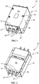
- the assembly 10 has a conductive enclosure 12 which surrounds and encloses electrical components therein.
- the enclosure 12 has a top wall 14, a bottom wall 16 and side walls 18 which extend between the top wall 14 and the bottom wall 16.
- a front wall or first mounting panel 20 and a back wall or second mounting panel (not shown) extend between the top wall 14 and the bottom wall 16.
- the front and back mounting panels also extend between the side walls 18.
- the conductive enclosure 12 is made from electrically conductive material to provide shielding to the electrical components used in the assembly 10.
- Bus bar-receiving openings 22 extend through the front wall 20. In the illustrative embodiment shown, three openings 22 are shown, but any number can be provided without departing from the scope of the invention.
- the openings 22 are dimensioned to receive insulators 24 and bus bars 26 therethrough.
- fastener receiving openings 28 are offset from the geometrical centerline of the bus bar 26, however other configurations can be used without departing from the scope of the invention.
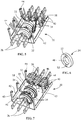
- a mounting plate 30 is provided in the conductive enclosure 12 between the two side walls 18.
- the mounting plate 30 has locating members or tabs 32 which are formed from a top surface 33 of the mounting plate 30.
- the tabs 32 extend from the top surface 33 at an acute angle which is less than 90 degrees, such as, but not limited to less than 60 degrees, less than 50 degrees, less than 40 degrees, greater than 10 degrees, greater than 20 degrees, approximately 20 degrees, approximately 30 degrees, approximately 40 degrees or any other angle in which two respective tabs 32 form a cradle to cooperate with inductive cores 34, as will be more fully described.
- Tabs 36 also extend from the top surface 33 of the mounting plate 30 at an angle which is approximately equal to 90 degrees or any other angle in which two respective tabs 36 form mounting guides to cooperate with cores 38, as will be more fully described.
- Mounting legs 40 extend from a sidewall 42 of the mounting plate 30.
- the sidewalls 42 extend from the top surface 33 in an essentially perpendicular direction.
- the sidewalls 42 are integral with and are formed from the top surface 33.
- three mounting legs 40 extend from each sidewall 42, although other numbers of mounting legs 40 can be used without departing from the scope of the invention.
- Circuit board mounting tabs 44 are provided at the ends of mounting legs 40.
- securing bands 46 are inserted proximate tabs 32, 36.
- the securing bands 46 are inserted through openings created when the tabs 32, 36 are formed from the top surface 33.
- the bands 46 are made from any material which has a sufficient melt/relaxation temperature to maintain the stiffness characteristics required. Such melt/relaxation temperature being greater than the maximum capacitor temperature, which in the embodiment shown is 110 degrees Celsius or the ferrite curie temperature, which in the embodiment shown is 140 degrees Celsius.
- Such material includes, but is not limited to pallet packing steel tape, bailing wire, other metal tape, and other metal wire.
- the inductive cores 34 are positioned proximate the respective tabs 32 (as best shown in FIG. 8 ).
- Padding 35 may be provided on the tabs 32.
- the padding 35 is made from any material which has a sufficient cushioning and which can withstand temperatures being greater than the maximum capacitor temperature, which in the embodiment shown is 110 degrees Celsius or the ferrite curie temperature, which in the embodiment shown is 140 degrees Celsius.
- the inductive cores 34 are magnetic cores, which may be of a high frequency ferrite composition. Each of these cores 34 includes a central opening 48. The openings 48 are aligned along a common axis. The bus bars 26 extend through the openings 48 as shown. Insulation 51 serves to electrically insulate the bus bars 26 from the cores 34. In the illustrative embodiment, four cores 34 are shown, with two respective cores 34 being positioned adjacent each other. The adjacent cores 34 being spaced apart by foam tape 52 ( FIG. 6 ). In the illustrative embodiment, the openings 48 are circular and receive three bus bars 26. However, other configurations of the openings 48 and other numbers of bus bars 26 can be used without departing from the scope of the invention.
- At least one wire 54 is secured to each of the bus bars 26.
- Each wire 54 has a terminal which is secured to a respective bus bar 26 by means of a screw. The screw compresses the terminal against the bus bar 26 thereby providing good electrical contact there between.
- Other known means of securing the wires 54 to the bus bars 26 can be used without departing from the scope of the invention.
- Inductive cores 38 are also positioned to cooperate with each of the bus bars 26.
- the cores 38 may be made from materials such as, but not limited to, silicon or powdered iron.
- the tabs 36 cooperate with the cores 38 to properly position the cores 38 and facilitate electrical isolation between the cores 38 and the bus bars 26.
- the bands 46 are deformed and tightened around the cores 34 and the cores 38 to form retention hoops.
- the bands 46 bend as they are tightened.
- a tightening tool (not shown) cooperates with a fastener 58 to constrict the bands 46 around the cores 34. The bands 46 are tightened until the hoops provide sufficient force to hold the cores 34 in position relative to the tabs 32 and the top surface 33, i.e. in the cradles.
- the tightening of the bands 46 is stopped prior to the bands 46 causing the deflection of the tabs 32 or just after the tabs 32 are deflected toward the cores 34.
- the controlled tightening prevents or limits the deformation of the bands 46 by the tabs 32 and causes the tabs 32 of the cradle to be deflected toward the cores 34, which in turn prevents the deformation of the cores 34 while properly maintain the inductive cores 34 in position in the cradles, thereby minimizing or eliminating magnetostriction of the cores 34. Consequently, the configuration of the cradle, i.e.
- the tabs 32 and the top surface 33 provides a visual and mechanical indication of the maximum tension to be applied to the bands 46, thereby establishing an appropriate hoop tension limit.
- the use of padding 35 while not required, can further protect the cores 34 from damage, eliminating or minimizing hertzian contact stresses between the cores 34 and the tabs 32.
- the positioning of the cores 34 adjacent to the tabs 32 causes the cores 34 to be precisely positioned relative to the mounting plate 30 and the enclosure 12.
- pairs of tabs 32 form cradles which receive cores 34 therein.
- Each core 34 mechanically engages each tab 32 of the pair of tabs and the top surface 33 of the mounting plate 30. This mechanical engagement provides sufficient mechanical contact to properly position each core 34 in a respective cradle, such that the opening 48 of each core 34 will align with the common axis.
- the use of the bands 46 ensures that the cores 34 will be properly maintained in position. This allows the cores 34 to be precisely located, allowing the assembly 10 to properly function as an electromagnetic interference filter while allowing the overall size of the assembly 10 to be reduced when compared to known electromagnetic filter assemblies.
- the bands 46 bend as they are tightened.
- a tool (not shown) cooperates with a fastener 58 to cause the bands 46 to tighten around the cores 38.
- the bands 46 are tightened until the bands 46 provide sufficient force to hold the cores 38 in position relative to the tabs 36 and the top surface 33.
- the controlled tightening of the bands 46 prevents the deformation of the mounting plate 30.
- the bands 46, and the cores 34 and 38 do not require the use of any type of potting compound to secure the cores 34 and 38 in the assembly 10.
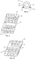
- a plurality of capacitors 60 and resistors 62 are mounted on a printed circuit board 64.
- the capacitors 60 and resistors 62 are mounted on a first surface 66 of the circuit board 64 and have leads which extend through the circuit board 64 to a second surface 68.
- the leads are bent to make contact with traces 70 and are soldered in position to maintain the electrical connection between the leads and the traces 70.
- Each of the (line-to-line) X-capacitors 60 and resistors 62 has a lead which is connected to a neutral trace, with a (line-to-ground) Y-capacitor connecting between the neutral trace and grounding trace 72 to provide the grounding required for operation.
- the circuit board 64 is mounted onto the circuit board mounting tabs 44 of the mounting legs 40 of the mounting plate 30.
- the circuit board 64 is maintained on the circuit board mounting tabs 44 by screws or other known mounting methods.
- Conductive members, such as, but not limited to wires 54 are provided in electrical engagement with the traces 70 of the circuit board 64.
- the wires 54 are soldered in position to maintain the electrical connection between the wires 54 and the traces 70. With the wires 54 and the leads of the capacitors 60 and resistors 62 properly secured to the traces 70, the capacitors 60 and resistors 62 are placed in electrical communication with the bus bars 26.
- the capacitors 60 and resistors 62 are precisely located on the circuit board 64, allowing the assembly 10 to properly function as an electromagnetic interference filter while allowing the overall size of the assembly 10 to be reduced when compared to known electromagnetic filter assemblies.
- the capacitors 60 and resistors 62 do not require the use of any type of potting compound to secure the capacitors 60 and resistors 62 in the assembly 10.
- the assembled mounting plate 30 and circuit board 64 are positioned and secured in the enclosure 12, as shown in FIGS 1 and 2 .
- Screw receiving openings 74 of the top wall 14 align with the grounding pads 72 of the circuit board 64. Screws are inserted into the openings 74 and the grounding pads 72, thereby placing the enclosure 12 in electrical engagement with the grounding pads 72 of the circuit board 64 to enhance the electromagnetic interference attenuation of the assembly 10.
- the grounding pads 72 are provided in electrical engagement with the electrical components of the filter assembly 10, proper and effective grounding for the components is easily accomplished by attaching the grounding pads 72 to a ground which is external of the filter assembly, thereby enhancing the electromagnetic interference attenuation of the assembly 10.
- the mounting plate 30 cooperates with the cores 34 and 38 to dissipate heat generated by the cores 34 and the cores 38.
- the mounting plate 30 conducts heat to the bottom wall 16 and side walls 18 so that the heat can be efficiently and effectively conducted to the outside of the enclosure 12 of the assembly 10.
- FIG. 12 is a schematic diagram 80 of the circuit formed by the components of the EMI filter assembly of FIGS. 1 through 11 .
- the assembly 10 is a multistage assembly for providing electromagnetic interference attenuation in which the electrical components are precisely located and stresses on the electrical components are reduced or eliminated.
- the assembly 10 is smaller in size and easier to assemble than the filters known in the art.
Landscapes
- Engineering & Computer Science (AREA)
- Power Engineering (AREA)
- Microelectronics & Electronic Packaging (AREA)
- Shielding Devices Or Components To Electric Or Magnetic Fields (AREA)
- Filters And Equalizers (AREA)
Claims (14)
- Baugruppe (10) zum Erzielen von elektromagnetischer Interferenzdämpfung, wobei die Baugruppe Folgendes umfasst:ein Gehäuse (12) mit einem ersten Paneel (20) und einem zweiten Paneel;Sammelschienen (26), die durch das erste Paneel und das zweite Paneel verlaufen;eine Montageplatte (30), die zwischen dem ersten Paneel und dem zweiten Paneel positioniert ist; undmehrere induktive Kerne (34, 38), wobei die induktiven Kerne Öffnungen (48) haben, durch die die Sammelschienen verlaufen,dadurch gekennzeichnet, dass sich auf der Montageplatte (30) Positionsgabeelemente (32, 36) befinden, wobei die Positionsgabeelemente Zungen (32, 36) sind, die sich von einer Oberfläche der Montageplatte (30) erstrecken, wobei Paare der Zungen jeweilige Aufnahmen bilden, in denen die induktiven Kerne (34, 38) positioniert werden, um dadurch die induktiven Kerne präzise in dem Gehäuse zu positionieren, um die elektromagnetische Interferenzdämpfung zu erleichtern.
- Baugruppe nach Anspruch 1, die ferner Folgendes umfasst:eine Leiterplatte (64);auf der Leiterplatte montierte Kondensatoren (60);leitende Elemente (54), die zwischen der Leiterplatte und den Sammelschienen verlaufen und diese elektrisch miteinander verbinden.
- Baugruppe nach Anspruch 1 oder 2, wobei ein oder mehrere Sicherungsstreifen (46) um die induktiven Kerne (34, 38) und die Zungen (32, 36) verlaufen und die Sicherungsbänder genügend Kraft bereitstellen, um die induktiven Kerne in den Aufnahmen festzuhalten, ohne die induktiven Kerne zu verformen, um dadurch Magnetostriktion der induktiven Kerne zu minimieren.
- Baugruppe nach Anspruch 3, wobei die Streifen (46) eine Entspannungstemperatur von mehr als 110 °C haben.
- Baugruppe nach Anspruch 3 oder 4, wobei die Streifen (46) ein Metallband oder Metalldraht sind.
- Baugruppe nach einem vorherigen Anspruch, wobei Polsterung (35) zwischen den Zungen (32, 36) und den induktiven Kernen (34, 38) bereitgestellt wird und wobei die Polsterung die Kerne vor Schäden aufgrund von Hertzschen Pressungen schützt.
- Baugruppe nach Anspruch 2 oder einem der Ansprüche 3 bis 6 in Abhängigkeit von Anspruch 2, wobei die Kondensatoren (60) Leitungen haben, die durch die Leiterplatte verlaufen und in elektrischem Eingriff mit Leiterbahnen (70) der Leiterplatte vorgesehen sind.
- Baugruppe nach Anspruch 2 oder einem der Ansprüche 3 bis 7 in Abhängigkeit von Anspruch 2, wobei Erdungsbahnen (72) in der Nähe von gegenüberliegenden Rändern der Leiterplatte vorgesehen sind.
- Baugruppe nach Anspruch 8, wobei die Erdungsbahnen (72) der Leiterplatte in elektrischem Eingriff mit dem Gehäuse (12) vorgesehen sind, um die elektromagnetische Interferenzdämpfung der Baugruppe zu verbessern.
- Baugruppe nach Anspruch 2 oder einem der Ansprüche 3 bis 9 in Abhängigkeit von Anspruch 2, wobei sich Montageschenkel (40) von der Montageplatte (30) erstrecken und wobei die Leiterplatte (64) auf den Montageschenkeln montiert ist.
- Baugruppe nach einem vorherigen Anspruch, wobei die Montageplatte (30) mit den induktiven Kernen (34, 38) zusammenwirkt, um durch die induktiven Kerne erzeugte Wärme zum Gehäuse zu leiten.
- Baugruppe nach einem vorherigen Anspruch, wobei das Gehäuse (12) aus elektrisch leitendem Material gefertigt ist und die induktiven Kerne (34, 38) umschließt, um elektromagnetische Abschirmung bereitzustellen.
- Baugruppe nach einem vorherigen Anspruch, wobei das Gehäuse ferner eine Deckwand (14), eine Bodenwand (16) und zwischen der Deck- und Bodenwand verlaufende Seitenwände (18) hat.
- Baugruppe nach Anspruch 13, wobei das erste und zweite Paneel jeweils zwischen der Deck- und der Bodenwand (14, 16) und auch zwischen den Seitenwänden (18) verlaufen.
Applications Claiming Priority (1)
| Application Number | Priority Date | Filing Date | Title |
|---|---|---|---|
| US14/186,144 US9276546B2 (en) | 2014-02-21 | 2014-02-21 | Electromagnetic interference filter assembly |
Publications (2)
| Publication Number | Publication Date |
|---|---|
| EP2911295A1 EP2911295A1 (de) | 2015-08-26 |
| EP2911295B1 true EP2911295B1 (de) | 2017-09-06 |
Family
ID=52473798
Family Applications (1)
| Application Number | Title | Priority Date | Filing Date |
|---|---|---|---|
| EP15155525.7A Active EP2911295B1 (de) | 2014-02-21 | 2015-02-18 | Filteranordnung gegen elektromagnetische Interferenz |
Country Status (3)
| Country | Link |
|---|---|
| US (1) | US9276546B2 (de) |
| EP (1) | EP2911295B1 (de) |
| CN (1) | CN104918471B (de) |
Cited By (1)
| Publication number | Priority date | Publication date | Assignee | Title |
|---|---|---|---|---|
| WO2024052222A1 (de) * | 2022-09-05 | 2024-03-14 | Magnetec Gmbh | Magnetfeldempfindliche baugruppe, induktives bauelement, platine mit induktivem bauelement, verwendung einer magnetfeldempfindlichen baugruppe |
Families Citing this family (14)
| Publication number | Priority date | Publication date | Assignee | Title |
|---|---|---|---|---|
| DE102014214021B4 (de) * | 2014-07-18 | 2017-01-05 | Conti Temic Microelectronic Gmbh | Filteranordnung zum Filtern von parasitären Induktionsströmen, Spannungswandler mit einer Filteranordnung |
| JP6379401B2 (ja) * | 2014-09-11 | 2018-08-29 | 北川工業株式会社 | 出力ノイズ低減装置 |
| JP2016072504A (ja) * | 2014-09-30 | 2016-05-09 | 北川工業株式会社 | 出力ノイズ低減装置 |
| JP2017069317A (ja) * | 2015-09-29 | 2017-04-06 | 北川工業株式会社 | ノイズ低減装置 |
| JP2017069675A (ja) * | 2015-09-29 | 2017-04-06 | 北川工業株式会社 | ノイズ低減装置 |
| JP6137280B2 (ja) * | 2015-11-20 | 2017-05-31 | 株式会社安川電機 | 電力変換装置 |
| DE102015224872A1 (de) * | 2015-12-10 | 2017-06-14 | Te Connectivity Germany Gmbh | Filterbaugruppe für Hochvoltverbinderanordnung und Hochvoltverbinderanordnung |
| DE202016104468U1 (de) * | 2016-08-12 | 2016-08-24 | Schaffner Emv Ag | Filter mit Leiterplatte und Stromschienen |
| DE102017204949B4 (de) * | 2017-03-23 | 2024-11-28 | SUMIDA Components & Modules GmbH | Induktives Bauelement und Verfahren zum Herstellen eines induktiven Bauelements |
| JP7200521B2 (ja) * | 2018-07-11 | 2023-01-10 | 京セラドキュメントソリューションズ株式会社 | 電装装置及び表示装置 |
| US11129286B2 (en) | 2018-07-12 | 2021-09-21 | Ppc Broadband, Inc. | Power supply noise suppressor |
| DE102020125923A1 (de) | 2020-10-04 | 2022-04-07 | EPA GmbH | Absorptionsfilter sowie Verfahren zur Herstellung eines solchen |
| CN115483570A (zh) | 2021-06-16 | 2022-12-16 | 福特全球技术公司 | 一种连接器总成 |
| US20240355539A1 (en) * | 2023-04-18 | 2024-10-24 | Steering Solutions Ip Holding Corporation | Header assembly with integrated choke for power pack |
Family Cites Families (15)
| Publication number | Priority date | Publication date | Assignee | Title |
|---|---|---|---|---|
| US4737745A (en) | 1986-11-03 | 1988-04-12 | Westinghouse Electric Corp. | Electromagnetic interference filter assembly |
| US5119266A (en) | 1989-12-29 | 1992-06-02 | Ail Systems, Inc. (Subsidiary Of Eaton Corp.) | Electromagnetic interference filter protection circuit |
| US5083101A (en) | 1990-01-03 | 1992-01-21 | Integrated Power Components | Integrated electromagnetic interference filter |
| US5195232A (en) | 1990-01-03 | 1993-03-23 | Integrated Power Components Inc. | Method of making electromagnetic interference filters |
| US5838216A (en) * | 1996-09-06 | 1998-11-17 | Sunstrand Corporation | Common-mode EMI filter |
| US6055164A (en) | 1997-11-13 | 2000-04-25 | Lucent Technologies Inc. | System and method for attenuating induced EMI and power converter employing the same |
| US6218913B1 (en) | 1998-02-18 | 2001-04-17 | Curtis Industries, A Division Of Powers Holatings, Inc. | Coaxial toroid EMI filter with discrete capacitors surrounding conductors |
| FR2819678B1 (fr) | 2001-01-12 | 2003-04-11 | Sagem | Circuit de filtrage, et dispositif d'alimentation de puissance equipe d'un tel circuit de filtrage |
| DE102005013509C5 (de) | 2004-03-30 | 2024-08-29 | Schaffner Emv Ag | EMV Filter |
| US7310242B2 (en) * | 2004-05-21 | 2007-12-18 | General Motors Corporation | Self-shielding high voltage distribution box |
| KR100798339B1 (ko) * | 2006-10-17 | 2008-01-28 | 엘에스산전 주식회사 | 기중차단기용 개폐기구의 투입 스프링 어셈블리 |
| CN201054848Y (zh) | 2006-12-31 | 2008-04-30 | 飞利浦(中国)投资有限公司 | 电磁干扰抑制装置、电子镇流器系统以及紧凑型节能灯 |
| JP2009127523A (ja) | 2007-11-22 | 2009-06-11 | Mitsubishi Heavy Ind Ltd | インバータ一体型電動圧縮機 |
| JP5687531B2 (ja) * | 2011-03-09 | 2015-03-18 | トヨタ自動車株式会社 | ノイズ低減装置およびバスバーモジュール |
| JP6286765B2 (ja) * | 2012-09-28 | 2018-03-07 | 北川工業株式会社 | ノイズフィルタ付バスバー装置 |
-
2014
- 2014-02-21 US US14/186,144 patent/US9276546B2/en active Active
-
2015
- 2015-02-17 CN CN201510156252.8A patent/CN104918471B/zh active Active
- 2015-02-18 EP EP15155525.7A patent/EP2911295B1/de active Active
Non-Patent Citations (1)
| Title |
|---|
| None * |
Cited By (1)
| Publication number | Priority date | Publication date | Assignee | Title |
|---|---|---|---|---|
| WO2024052222A1 (de) * | 2022-09-05 | 2024-03-14 | Magnetec Gmbh | Magnetfeldempfindliche baugruppe, induktives bauelement, platine mit induktivem bauelement, verwendung einer magnetfeldempfindlichen baugruppe |
Also Published As
| Publication number | Publication date |
|---|---|
| US9276546B2 (en) | 2016-03-01 |
| US20150244339A1 (en) | 2015-08-27 |
| CN104918471B (zh) | 2019-02-05 |
| CN104918471A (zh) | 2015-09-16 |
| EP2911295A1 (de) | 2015-08-26 |
Similar Documents
| Publication | Publication Date | Title |
|---|---|---|
| US9276546B2 (en) | Electromagnetic interference filter assembly | |
| CN107742976B (zh) | 滤波器和车辆 | |
| US4401355A (en) | Filtered connector | |
| US3594613A (en) | Transformer connection | |
| CN113363753B (zh) | 电缆连接器 | |
| US6036505A (en) | Mechanism for connecting printed circuit boards of separate devices | |
| CN109256265B (zh) | 电抗器 | |
| US8063727B2 (en) | Conductive shielding device | |
| US9906200B2 (en) | Power filter | |
| KR20220133192A (ko) | Emc 필터 플러그인 장치 | |
| EP3704766B1 (de) | Modul für hochstromstecker und/oder hochstromkabel, hochstromstecker und verfahren zur beeinflussung des emv-verhaltens | |
| US7361030B2 (en) | Mounting structure of high frequency apparatus | |
| CN105763038A (zh) | 功率转换装置 | |
| EP3218969B1 (de) | Leitungsfilter und verfahren zur installation eines leitungsfilters auf einem systemkabel | |
| CN113711705A (zh) | 电子控制装置 | |
| KR20130057142A (ko) | 접지 스프링 | |
| US10950985B2 (en) | Shield connection element for a printed circuit board | |
| CN222888050U (zh) | 储能变流器 | |
| US8477513B2 (en) | Electrical connector shield | |
| KR102316690B1 (ko) | 동축 커넥터 | |
| JP2011129747A (ja) | 高周波機器用のコイル及び該コイルを備える高周波機器 | |
| CN119602029A (zh) | 连接器及电子设备的配件 | |
| CN104380851B (zh) | 制造过程优化的滤波装置 | |
| JPH0983176A (ja) | 電子機器 | |
| Kimmel et al. | Connectors are a major EMI weakness. |
Legal Events
| Date | Code | Title | Description |
|---|---|---|---|
| PUAI | Public reference made under article 153(3) epc to a published international application that has entered the european phase |
Free format text: ORIGINAL CODE: 0009012 |
|
| AK | Designated contracting states |
Kind code of ref document: A1 Designated state(s): AL AT BE BG CH CY CZ DE DK EE ES FI FR GB GR HR HU IE IS IT LI LT LU LV MC MK MT NL NO PL PT RO RS SE SI SK SM TR |
|
| AX | Request for extension of the european patent |
Extension state: BA ME |
|
| 17P | Request for examination filed |
Effective date: 20160226 |
|
| RBV | Designated contracting states (corrected) |
Designated state(s): AL AT BE BG CH CY CZ DE DK EE ES FI FR GB GR HR HU IE IS IT LI LT LU LV MC MK MT NL NO PL PT RO RS SE SI SK SM TR |
|
| RAP1 | Party data changed (applicant data changed or rights of an application transferred) |
Owner name: TE CONNECTIVITY CORPORATION |
|
| GRAP | Despatch of communication of intention to grant a patent |
Free format text: ORIGINAL CODE: EPIDOSNIGR1 |
|
| STAA | Information on the status of an ep patent application or granted ep patent |
Free format text: STATUS: GRANT OF PATENT IS INTENDED |
|
| RIC1 | Information provided on ipc code assigned before grant |
Ipc: H01F 27/26 20060101ALN20170203BHEP Ipc: H03H 1/00 20060101AFI20170203BHEP Ipc: H03H 7/01 20060101ALI20170203BHEP Ipc: H01F 17/06 20060101ALN20170203BHEP Ipc: H03H 7/42 20060101ALI20170203BHEP |
|
| INTG | Intention to grant announced |
Effective date: 20170303 |
|
| GRAS | Grant fee paid |
Free format text: ORIGINAL CODE: EPIDOSNIGR3 |
|
| GRAJ | Information related to disapproval of communication of intention to grant by the applicant or resumption of examination proceedings by the epo deleted |
Free format text: ORIGINAL CODE: EPIDOSDIGR1 |
|
| GRAL | Information related to payment of fee for publishing/printing deleted |
Free format text: ORIGINAL CODE: EPIDOSDIGR3 |
|
| STAA | Information on the status of an ep patent application or granted ep patent |
Free format text: STATUS: REQUEST FOR EXAMINATION WAS MADE |
|
| GRAR | Information related to intention to grant a patent recorded |
Free format text: ORIGINAL CODE: EPIDOSNIGR71 |
|
| STAA | Information on the status of an ep patent application or granted ep patent |
Free format text: STATUS: GRANT OF PATENT IS INTENDED |
|
| GRAA | (expected) grant |
Free format text: ORIGINAL CODE: 0009210 |
|
| STAA | Information on the status of an ep patent application or granted ep patent |
Free format text: STATUS: THE PATENT HAS BEEN GRANTED |
|
| INTC | Intention to grant announced (deleted) | ||
| RIC1 | Information provided on ipc code assigned before grant |
Ipc: H03H 7/42 20060101ALI20170707BHEP Ipc: H01F 27/26 20060101ALN20170707BHEP Ipc: H03H 1/00 20060101AFI20170707BHEP Ipc: H01F 17/06 20060101ALN20170707BHEP Ipc: H03H 7/01 20060101ALI20170707BHEP |
|
| INTG | Intention to grant announced |
Effective date: 20170727 |
|
| AK | Designated contracting states |
Kind code of ref document: B1 Designated state(s): AL AT BE BG CH CY CZ DE DK EE ES FI FR GB GR HR HU IE IS IT LI LT LU LV MC MK MT NL NO PL PT RO RS SE SI SK SM TR |
|
| REG | Reference to a national code |
Ref country code: GB Ref legal event code: FG4D |
|
| REG | Reference to a national code |
Ref country code: CH Ref legal event code: EP Ref country code: AT Ref legal event code: REF Ref document number: 926915 Country of ref document: AT Kind code of ref document: T Effective date: 20170915 |
|
| REG | Reference to a national code |
Ref country code: IE Ref legal event code: FG4D |
|
| REG | Reference to a national code |
Ref country code: DE Ref legal event code: R096 Ref document number: 602015004507 Country of ref document: DE |
|
| REG | Reference to a national code |
Ref country code: NL Ref legal event code: MP Effective date: 20170906 |
|
| REG | Reference to a national code |
Ref country code: FR Ref legal event code: PLFP Year of fee payment: 4 |
|
| REG | Reference to a national code |
Ref country code: LT Ref legal event code: MG4D |
|
| PG25 | Lapsed in a contracting state [announced via postgrant information from national office to epo] |
Ref country code: NO Free format text: LAPSE BECAUSE OF FAILURE TO SUBMIT A TRANSLATION OF THE DESCRIPTION OR TO PAY THE FEE WITHIN THE PRESCRIBED TIME-LIMIT Effective date: 20171206 Ref country code: LT Free format text: LAPSE BECAUSE OF FAILURE TO SUBMIT A TRANSLATION OF THE DESCRIPTION OR TO PAY THE FEE WITHIN THE PRESCRIBED TIME-LIMIT Effective date: 20170906 Ref country code: HR Free format text: LAPSE BECAUSE OF FAILURE TO SUBMIT A TRANSLATION OF THE DESCRIPTION OR TO PAY THE FEE WITHIN THE PRESCRIBED TIME-LIMIT Effective date: 20170906 Ref country code: FI Free format text: LAPSE BECAUSE OF FAILURE TO SUBMIT A TRANSLATION OF THE DESCRIPTION OR TO PAY THE FEE WITHIN THE PRESCRIBED TIME-LIMIT Effective date: 20170906 Ref country code: SE Free format text: LAPSE BECAUSE OF FAILURE TO SUBMIT A TRANSLATION OF THE DESCRIPTION OR TO PAY THE FEE WITHIN THE PRESCRIBED TIME-LIMIT Effective date: 20170906 |
|
| REG | Reference to a national code |
Ref country code: AT Ref legal event code: MK05 Ref document number: 926915 Country of ref document: AT Kind code of ref document: T Effective date: 20170906 |
|
| PG25 | Lapsed in a contracting state [announced via postgrant information from national office to epo] |
Ref country code: BG Free format text: LAPSE BECAUSE OF FAILURE TO SUBMIT A TRANSLATION OF THE DESCRIPTION OR TO PAY THE FEE WITHIN THE PRESCRIBED TIME-LIMIT Effective date: 20171206 Ref country code: ES Free format text: LAPSE BECAUSE OF FAILURE TO SUBMIT A TRANSLATION OF THE DESCRIPTION OR TO PAY THE FEE WITHIN THE PRESCRIBED TIME-LIMIT Effective date: 20170906 Ref country code: RS Free format text: LAPSE BECAUSE OF FAILURE TO SUBMIT A TRANSLATION OF THE DESCRIPTION OR TO PAY THE FEE WITHIN THE PRESCRIBED TIME-LIMIT Effective date: 20170906 Ref country code: LV Free format text: LAPSE BECAUSE OF FAILURE TO SUBMIT A TRANSLATION OF THE DESCRIPTION OR TO PAY THE FEE WITHIN THE PRESCRIBED TIME-LIMIT Effective date: 20170906 Ref country code: GR Free format text: LAPSE BECAUSE OF FAILURE TO SUBMIT A TRANSLATION OF THE DESCRIPTION OR TO PAY THE FEE WITHIN THE PRESCRIBED TIME-LIMIT Effective date: 20171207 |
|
| PG25 | Lapsed in a contracting state [announced via postgrant information from national office to epo] |
Ref country code: NL Free format text: LAPSE BECAUSE OF FAILURE TO SUBMIT A TRANSLATION OF THE DESCRIPTION OR TO PAY THE FEE WITHIN THE PRESCRIBED TIME-LIMIT Effective date: 20170906 |
|
| PG25 | Lapsed in a contracting state [announced via postgrant information from national office to epo] |
Ref country code: PL Free format text: LAPSE BECAUSE OF FAILURE TO SUBMIT A TRANSLATION OF THE DESCRIPTION OR TO PAY THE FEE WITHIN THE PRESCRIBED TIME-LIMIT Effective date: 20170906 Ref country code: RO Free format text: LAPSE BECAUSE OF FAILURE TO SUBMIT A TRANSLATION OF THE DESCRIPTION OR TO PAY THE FEE WITHIN THE PRESCRIBED TIME-LIMIT Effective date: 20170906 Ref country code: CZ Free format text: LAPSE BECAUSE OF FAILURE TO SUBMIT A TRANSLATION OF THE DESCRIPTION OR TO PAY THE FEE WITHIN THE PRESCRIBED TIME-LIMIT Effective date: 20170906 |
|
| PG25 | Lapsed in a contracting state [announced via postgrant information from national office to epo] |
Ref country code: EE Free format text: LAPSE BECAUSE OF FAILURE TO SUBMIT A TRANSLATION OF THE DESCRIPTION OR TO PAY THE FEE WITHIN THE PRESCRIBED TIME-LIMIT Effective date: 20170906 Ref country code: AT Free format text: LAPSE BECAUSE OF FAILURE TO SUBMIT A TRANSLATION OF THE DESCRIPTION OR TO PAY THE FEE WITHIN THE PRESCRIBED TIME-LIMIT Effective date: 20170906 Ref country code: SK Free format text: LAPSE BECAUSE OF FAILURE TO SUBMIT A TRANSLATION OF THE DESCRIPTION OR TO PAY THE FEE WITHIN THE PRESCRIBED TIME-LIMIT Effective date: 20170906 Ref country code: IS Free format text: LAPSE BECAUSE OF FAILURE TO SUBMIT A TRANSLATION OF THE DESCRIPTION OR TO PAY THE FEE WITHIN THE PRESCRIBED TIME-LIMIT Effective date: 20180106 Ref country code: IT Free format text: LAPSE BECAUSE OF FAILURE TO SUBMIT A TRANSLATION OF THE DESCRIPTION OR TO PAY THE FEE WITHIN THE PRESCRIBED TIME-LIMIT Effective date: 20170906 Ref country code: SM Free format text: LAPSE BECAUSE OF FAILURE TO SUBMIT A TRANSLATION OF THE DESCRIPTION OR TO PAY THE FEE WITHIN THE PRESCRIBED TIME-LIMIT Effective date: 20170906 |
|
| REG | Reference to a national code |
Ref country code: DE Ref legal event code: R097 Ref document number: 602015004507 Country of ref document: DE |
|
| PLBE | No opposition filed within time limit |
Free format text: ORIGINAL CODE: 0009261 |
|
| STAA | Information on the status of an ep patent application or granted ep patent |
Free format text: STATUS: NO OPPOSITION FILED WITHIN TIME LIMIT |
|
| PG25 | Lapsed in a contracting state [announced via postgrant information from national office to epo] |
Ref country code: DK Free format text: LAPSE BECAUSE OF FAILURE TO SUBMIT A TRANSLATION OF THE DESCRIPTION OR TO PAY THE FEE WITHIN THE PRESCRIBED TIME-LIMIT Effective date: 20170906 |
|
| 26N | No opposition filed |
Effective date: 20180607 |
|
| PG25 | Lapsed in a contracting state [announced via postgrant information from national office to epo] |
Ref country code: SI Free format text: LAPSE BECAUSE OF FAILURE TO SUBMIT A TRANSLATION OF THE DESCRIPTION OR TO PAY THE FEE WITHIN THE PRESCRIBED TIME-LIMIT Effective date: 20170906 |
|
| REG | Reference to a national code |
Ref country code: CH Ref legal event code: PL |
|
| PG25 | Lapsed in a contracting state [announced via postgrant information from national office to epo] |
Ref country code: MC Free format text: LAPSE BECAUSE OF FAILURE TO SUBMIT A TRANSLATION OF THE DESCRIPTION OR TO PAY THE FEE WITHIN THE PRESCRIBED TIME-LIMIT Effective date: 20170906 |
|
| REG | Reference to a national code |
Ref country code: IE Ref legal event code: MM4A |
|
| REG | Reference to a national code |
Ref country code: BE Ref legal event code: MM Effective date: 20180228 |
|
| PG25 | Lapsed in a contracting state [announced via postgrant information from national office to epo] |
Ref country code: LU Free format text: LAPSE BECAUSE OF NON-PAYMENT OF DUE FEES Effective date: 20180218 Ref country code: LI Free format text: LAPSE BECAUSE OF NON-PAYMENT OF DUE FEES Effective date: 20180228 Ref country code: CH Free format text: LAPSE BECAUSE OF NON-PAYMENT OF DUE FEES Effective date: 20180228 |
|
| PG25 | Lapsed in a contracting state [announced via postgrant information from national office to epo] |
Ref country code: IE Free format text: LAPSE BECAUSE OF NON-PAYMENT OF DUE FEES Effective date: 20180218 |
|
| PG25 | Lapsed in a contracting state [announced via postgrant information from national office to epo] |
Ref country code: BE Free format text: LAPSE BECAUSE OF NON-PAYMENT OF DUE FEES Effective date: 20180228 |
|
| PG25 | Lapsed in a contracting state [announced via postgrant information from national office to epo] |
Ref country code: MT Free format text: LAPSE BECAUSE OF NON-PAYMENT OF DUE FEES Effective date: 20180218 |
|
| PG25 | Lapsed in a contracting state [announced via postgrant information from national office to epo] |
Ref country code: TR Free format text: LAPSE BECAUSE OF FAILURE TO SUBMIT A TRANSLATION OF THE DESCRIPTION OR TO PAY THE FEE WITHIN THE PRESCRIBED TIME-LIMIT Effective date: 20170906 |
|
| PG25 | Lapsed in a contracting state [announced via postgrant information from national office to epo] |
Ref country code: PT Free format text: LAPSE BECAUSE OF FAILURE TO SUBMIT A TRANSLATION OF THE DESCRIPTION OR TO PAY THE FEE WITHIN THE PRESCRIBED TIME-LIMIT Effective date: 20170906 |
|
| PG25 | Lapsed in a contracting state [announced via postgrant information from national office to epo] |
Ref country code: MK Free format text: LAPSE BECAUSE OF NON-PAYMENT OF DUE FEES Effective date: 20170906 Ref country code: HU Free format text: LAPSE BECAUSE OF FAILURE TO SUBMIT A TRANSLATION OF THE DESCRIPTION OR TO PAY THE FEE WITHIN THE PRESCRIBED TIME-LIMIT; INVALID AB INITIO Effective date: 20150218 Ref country code: CY Free format text: LAPSE BECAUSE OF FAILURE TO SUBMIT A TRANSLATION OF THE DESCRIPTION OR TO PAY THE FEE WITHIN THE PRESCRIBED TIME-LIMIT Effective date: 20170906 |
|
| PG25 | Lapsed in a contracting state [announced via postgrant information from national office to epo] |
Ref country code: AL Free format text: LAPSE BECAUSE OF FAILURE TO SUBMIT A TRANSLATION OF THE DESCRIPTION OR TO PAY THE FEE WITHIN THE PRESCRIBED TIME-LIMIT Effective date: 20170906 |
|
| REG | Reference to a national code |
Ref country code: GB Ref legal event code: 732E Free format text: REGISTERED BETWEEN 20250731 AND 20250806 |
|
| PGFP | Annual fee paid to national office [announced via postgrant information from national office to epo] |
Ref country code: FR Payment date: 20251208 Year of fee payment: 12 |
|
| PGFP | Annual fee paid to national office [announced via postgrant information from national office to epo] |
Ref country code: GB Payment date: 20260106 Year of fee payment: 12 |
|
| PGFP | Annual fee paid to national office [announced via postgrant information from national office to epo] |
Ref country code: DE Payment date: 20251224 Year of fee payment: 12 |