EP2919362B1 - Verbessertes system und verfahren zur speisung eines drahtlosen fühlers. - Google Patents
Verbessertes system und verfahren zur speisung eines drahtlosen fühlers. Download PDFInfo
- Publication number
- EP2919362B1 EP2919362B1 EP15157699.8A EP15157699A EP2919362B1 EP 2919362 B1 EP2919362 B1 EP 2919362B1 EP 15157699 A EP15157699 A EP 15157699A EP 2919362 B1 EP2919362 B1 EP 2919362B1
- Authority
- EP
- European Patent Office
- Prior art keywords
- generating
- transistor
- electrical energy
- current
- sensor
- Prior art date
- Legal status (The legal status is an assumption and is not a legal conclusion. Google has not performed a legal analysis and makes no representation as to the accuracy of the status listed.)
- Active
Links
Images

Classifications
-
- G—PHYSICS
- G05—CONTROLLING; REGULATING
- G05F—SYSTEMS FOR REGULATING ELECTRIC OR MAGNETIC VARIABLES
- G05F1/00—Automatic systems in which deviations of an electric quantity from one or more predetermined values are detected at the output of the system and fed back to a device within the system to restore the detected quantity to its predetermined value or values, i.e. retroactive systems
- G05F1/10—Regulating voltage or current
- G05F1/46—Regulating voltage or current wherein the variable actually regulated by the final control device is DC
- G05F1/56—Regulating voltage or current wherein the variable actually regulated by the final control device is DC using semiconductor devices in series with the load as final control devices
-
- H—ELECTRICITY
- H02—GENERATION; CONVERSION OR DISTRIBUTION OF ELECTRIC POWER
- H02J—ELECTRIC POWER NETWORKS; CIRCUIT ARRANGEMENTS OR SYSTEMS FOR SUPPLYING OR DISTRIBUTING ELECTRIC POWER; SYSTEMS FOR STORING ELECTRIC ENERGY
- H02J50/00—Circuit arrangements or systems for wireless supply or distribution of electric power
- H02J50/30—Circuit arrangements or systems for wireless supply or distribution of electric power using light, e.g. lasers
-
- H—ELECTRICITY
- H02—GENERATION; CONVERSION OR DISTRIBUTION OF ELECTRIC POWER
- H02J—ELECTRIC POWER NETWORKS; CIRCUIT ARRANGEMENTS OR SYSTEMS FOR SUPPLYING OR DISTRIBUTING ELECTRIC POWER; SYSTEMS FOR STORING ELECTRIC ENERGY
- H02J7/00—Circuit arrangements for charging or discharging batteries or for supplying loads from batteries
- H02J7/02—Circuit arrangements for charging or discharging batteries or for supplying loads from batteries for charging batteries from AC mains by converters
-
- H—ELECTRICITY
- H02—GENERATION; CONVERSION OR DISTRIBUTION OF ELECTRIC POWER
- H02J—ELECTRIC POWER NETWORKS; CIRCUIT ARRANGEMENTS OR SYSTEMS FOR SUPPLYING OR DISTRIBUTING ELECTRIC POWER; SYSTEMS FOR STORING ELECTRIC ENERGY
- H02J7/00—Circuit arrangements for charging or discharging batteries or for supplying loads from batteries
- H02J7/34—Parallel operation in networks using both storage and other DC sources, e.g. providing buffering
-
- H—ELECTRICITY
- H02—GENERATION; CONVERSION OR DISTRIBUTION OF ELECTRIC POWER
- H02J—ELECTRIC POWER NETWORKS; CIRCUIT ARRANGEMENTS OR SYSTEMS FOR SUPPLYING OR DISTRIBUTING ELECTRIC POWER; SYSTEMS FOR STORING ELECTRIC ENERGY
- H02J7/00—Circuit arrangements for charging or discharging batteries or for supplying loads from batteries
- H02J7/34—Parallel operation in networks using both storage and other DC sources, e.g. providing buffering
- H02J7/345—Parallel operation in networks using both storage and other DC sources, e.g. providing buffering using capacitors as storage or buffering devices
Definitions
- the present application relates to the field of power supply devices for sensor assemblies equipped with a wireless communication system and whose electrical energy supply is partially due to a generator making it possible to recover a surrounding energy from the sensor assembly and to produce accordingly electrical energy.
- the document EP 2 395 594 A1 has a power supply device for supplying a sensor assembly by means of electrical energy charged to a buffer capacitor.
- the power device is provided with a first photovoltaic type generator which can be supplemented, in case of low illumination or zero illumination, by a second electrochemical generator in the form of a rechargeable battery.
- a system for managing and controlling the charge of the rechargeable battery is provided to make the sensor assembly functional even after a long period of time without illumination.
- Rechargeable batteries have the disadvantage of having a limited life and a reduced electrical load capacity.
- the document US 7 132 757 B2 presents meanwhile a device for supplying a sensor comprising a first generator for recovering a mechanical energy that it transforms into electrical energy and an electrochemical generator for supplying the first generator.
- the electrochemical generator is of the non-rechargeable type and in the form of a battery.
- a circuit makes it possible to connect the battery directly to the sensor when the electrical energy produced by the first generator is insufficient.
- This circuit has the disadvantage of being a consumer of electrical energy and can be expensive when it includes a microcontroller.
- a zener diode is provided.
- Such a diode has the main disadvantage of having a reverse current, of the order of several microamperes, which significantly increases the current consumption of the device.
- the document US 2009/0026842 has a power device with a solar panel configured so that when the power level delivered by the solar panel is below a given threshold, a battery serves as backup power.
- the electrical energy management circuit thus has a very low consumption, which is particularly advantageous for powering a wireless device whose supply of electrical energy depends on a recovery of surrounding energy.
- the arrangement of the unipolar transistor may also be provided so that its drain-source voltage depends on a difference between the electrical energy produced by the first generating means and the given supply level.
- the voltage V DD is maintained at a level below a predetermined threshold V MAXC1 while limiting the consumption of the supply device.
- the arrangement of the transistor is such that the threshold V MAXC1 depends on the voltage delivered by the battery which is predetermined and depends on the selected cell, and the clamping voltage of the transistor which is predetermined and also depends on the selected transistor.
- the unipolar transistor defined above is a JFET (for Junction Field Effect Transistor) transistor.
- a JFET for Junction Field Effect Transistor
- Such a transistor has the advantage of having an intrinsic gate-source junction that can be used to pass electrical current in a single direction from the battery to the storage capacitor while limiting its return to the stack.
- the unipolar transistor defined above is a depletion MOSFET transistor (also called depletion transistor).
- the depletion JFET and MOSFET transistors have, contrary to more commonly used enhancement MOS transistors, a conductive channel when their gate-source voltage is zero.
- the electrical energy management circuit may also include means for blocking a current return to the second generator means, in order to protect the latter while allowing a current flow in the opposite direction.
- the unipolar transistor defined above is a JFET transistor
- the intrinsic junction between its gate and its channel forms a means for blocking a current return to the stack.
- the intrinsic junction can also be used to recharge the storage capacitor from the stack when the V DD power level is low.
- a diode disposed between the gate and the source of the unipolar transistor may also form a means for blocking a current return to the second generator means. This diode can also be used to recharge the storage capacitor from the battery when the power level V DD is low.
- the second generating means may comprise or be associated with means for limiting a discharge current of the battery, for example in the form of at least one series resistance with the battery.
- means for limiting a current through the intrinsic junction between the gate and the channel of the JFET transistor may be provided, for example in the form of at least one resistor connected to the gate of the transistor.
- the supply device may further comprise means for blocking a current return to the first generator means, for example in the form of at least one diode.
- the first generating means may comprise a photovoltaic module.
- the present invention further provides a wireless sensor assembly comprising a power supply device as defined above.
- the sensor assembly can thus be provided with at least one sensor of at least one physical quantity to be measured and a radio frequency module designed to carry out wireless communications, in particular for transmitting to an external device data relating to measurements made by the sensor.
- the sensor assembly may also include a circuit for processing measurement data of the physical magnitude (s) measured from the sensor and transmitting this data to the RF module.
- the sensor assembly may advantageously comprise one or more of the sensors of the following physical quantities: humidity sensor, temperature sensor, brightness sensor, gas sensor, in particular CO 2 .
- the invention also relates to a method of supplying a wireless sensor assembly using a feeding device as defined above.
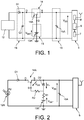
- the figure 1 represents a diagram of a supply device according to one embodiment of the invention.
- This power device serves to supply a sensor assembly 5 comprising one or more sensors 7, and which may be provided with a processing circuit 6 and an RF module 8.
- the sensor assembly 5 is configured to establish wireless communications with an external device (not shown) and relating to measurements by the sensor (s) 7.
- the supply device can be provided to deliver a supply of electrical energy to the sensor assembly 5, in the form of current peaks, corresponding in particular to times when the sensor assembly 5 makes measurements or communicates with the outside. .
- the supply device comprises a first generator means 12 adapted to recover a so-called "ambient" energy that is in the environment of the sensor assembly 5 and to convert this ambient energy into electrical energy used to power the sensor assembly 5
- the recovered ambient energy may be, for example, thermal, and / or mechanical, and / or electromechanical energy, and / or light energy.
- the first generator means 12 for energy recovery is advantageously a photovoltaic module.
- a rectifier block 19 may be provided at the output of the first generator means 12. Such a block 19 also makes it possible to prevent current discharge to the first generator means 12, in particular in a case where the electrical energy produced by the latter is small.
- This block 19 may thus comprise a diode D1 with a low threshold voltage V F , for example of the order of 0.3V such as a Schottky diode or a diode bridge (not shown).
- the rectifier block 19 may also be provided with one or more filter capacitors C 2 .
- the first generating means 12 is associated with electrical energy storage means 15 formed here of at least one capacitor 15A, the stored energy of which serves to supply the sensor assembly 5.
- a capacitor 15A advantageously makes it possible to perform a significant number of charge and discharge cycles.
- the capacitor 15A used is preferably a low-current self-discharge capacitor, for example a ceramic capacitor.
- the charges and discharges of the storage capacitor 15A are controlled so as to ensure a good supply level V DD to the sensor unit 5, that is to say to a supply level V DD which is greater than one. terminal or at a threshold predetermined, in particular a minimum voltage V minc1 necessary for the operation of the sensor assembly 5.
- the supply level V DD is furthermore controlled so as to remain below a terminal or a threshold, in particular a maximum voltage V MAXc1 predetermined according to the maximum voltage supported by the components of the sensor assembly 5.
- the voltage V MAXc1 maximum is also provided sufficiently low to limit the consumption of the power device.
- the power supply device can adopt a configuration in which the generator means 12 recharges the capacitor 15A, while in the absence of ambient energy, the power supply device is likely to adopt another configuration in which the capacitor 15A is recharged using an electrochemical generator 13 booster.
- a backup generator comprising a battery 13A, ie a non-rechargeable electrochemical generator, whose lifetime and current capacity are greater than those of a battery of the same technology.
- the battery 13A can be for example lithium ie with a lithium or lithium compound anode, for example a battery referenced CR2016 having a voltage delivered of the order of 3V and an electric charge capacity of the order of 80 mAh , or for example a battery referenced CR1220.
- the control of the charge and the discharge of the capacitor 15A and the supply level V DD of the sensor assembly 5 is ensured by means of an electrical energy management circuit.
- the management circuit comprises a unipolar transistor 14 of the conductive channel type delivering a non-zero current I DS when its gate-source voltage V GS is zero.
- a unipolar transistor may be of JFET or depletion MOSFET type (also called depletion MOSFET).
- the arrangement of the electrical energy management circuit, and in particular that of the unipolar transistor 14, is such that the gate-source voltage between the gate G and the source S of this transistor 14A depends on the difference between a voltage V BAT delivered. by the auxiliary electrochemical generator 13 and the voltage V DD across the terminals of the capacitor 15A and which is applied to the sensor assembly 5.
- the gate of the unipolar transistor 14 is connected to the battery 13A while its source is connected to a terminal of the storage capacitor 15A.
- the drain-source current level Ids that the transistor 14 delivers is controlled by the difference between the charge level of the capacitor 15A and the voltage delivered by the non-rechargeable electrochemical generator.
- the unipolar transistor 14 is also arranged to have a drain on which the electrical energy produced by the first generator means 12 is applied.
- the drain-source voltage between the drain D and the source S of the transistor 14A depends on the difference between the voltage generated by the first generator means 12 and the energy stored across the capacitor 15A.
- the unipolar transistor 14 whose channel is conductive and delivers a non-zero current I DS when its gate-source voltage V GS is zero, is thus provided to control the variations of the voltage V DD across the capacitor, particularly limiting the level maximum of this voltage V DD applied to the sensor assembly.
- the control of the voltage V DD is achieved by a management of the respective supply of electrical energy from the first generator means 12 and the electrochemical generator 13 booster.
- the unipolar transistor is a JFET transistor type JFET (JFET for Junction Field Effect Transistor) with an N-doped channel.
- JFET transistor type JFET JFET for Junction Field Effect Transistor
- Such a type of transistor has the advantage of having a junction in its gate and its channel, also called an intrinsic junction. Or “intrinsic diode” that can be used for charging the storage capacitor 15A to the stack 13A.
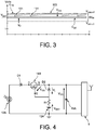
- a particular embodiment of the feed device is illustrated on the figure 2 , with a first generator means 12 comprising a photovoltaic module 12A, and at the output of this module means, for example in the form of a diode D 1 , for blocking a current return to the photovoltaic module 12A.
- a first generator means 12 comprising a photovoltaic module 12A, and at the output of this module means, for example in the form of a diode D 1 , for blocking a current return to the photovoltaic module 12A.
- This example differs from that described above in that means for blocking a current return to the battery 13A, are here formed using a diode D2 between the gate and the source of transistor 14A.
- the diode D2 may be a Schottky diode, which has the advantage of having a low threshold voltage V F , for example of the order of 0.3V. This diode makes it possible to pass electric current in a single direction from the battery to the storage capacitor with low voltage drop.
- the supply device further comprises means for limiting the current delivered by the battery 13A in the form, for example, of at least one resistor R 1 in series with the battery 13A, as well as means for limiting the current in the intrinsic diode or junction of the transistor 14A JFET in the form of, for example, at least one resistor R 2 connected to the gate of the latter.
- the gate-source voltage V GS of the transistor 14A is such that the latter is conducting in order to allow the capacitor to be recharged by the battery.
- the gate-source voltage V GS of the transistor 14A is such that the latter is conducting in order to allow the capacitor 12 to recharge the capacitor.
- the transistor 14A blocks the current reloading the capacitor 15A.
- the electrical energy management circuit thus prevents the creation of an overvoltage in the supply V DD applied to the sensor assembly 5A.
- the capacitor 15A is recharged from the battery 13A through the diode D2 and the resistor R1 when V DD ⁇ V BAT - V F with V F the threshold voltage of the diode D2.
- the transistor 14A remains on and the diode D1 protects the photovoltaic module 12A against a current return.
- the resistor R2 makes it possible to limit the current flow through the intrinsic diode of the transistor 14A for a case where the voltage across the capacitor 15A is such that V DD ⁇ V BAT - V F , with V F is the smallest voltage of the capacitor.
- threshold of the diode D2 and / or the intrinsic diode of the JFET transistor 14A is the smallest voltage of the capacitor.
- the intrinsic diode existing between its gate and its channel can be used in place of the diode D2 as in the example shown on the figure 1 the resistance R2 is then also optional.
- the inverse current I GSS of the diode D2 and / or the intrinsic diode of the JFET transistor 14A is generally very low, for example of the order 1 nA.
- the current I GSS represents the only static consumption of the energy management circuit which is much lower than the static consumption of solutions based on a zener diode or a linear regulator of the LDO voltage (for "low-dropout").
- a reverse leakage current of a zener diode limiting a voltage to 3.3V can be of the order of 5 ⁇ A, ie much higher than a current I GSS 1nA and even higher than the average current consumed some wireless sensors.
- V MiNC 1 V BAT - V F - R 1 + ESR BAT * I DD MAX , with I DD_MAX a maximum current consumed by the sensor assembly 5, ESR BAT the internal resistance of the battery, V F the threshold voltage of the diode D2, which can be equal to about 0.3 V for a Schottky diode.
- the figure 3 illustrates variations in the voltage V DD supplied at the output of the power supply device previously described in the presence of illumination.
- Current peaks (sudden variations 101 on the curve C 10 ) are consumed by the sensor assembly 5 at the times when it makes measurements and / or radio communication. Between these instants (stable portion 103 on the curve C 10 ) the sensor assembly is in standby.
- the photovoltaic module 12A thus directly recharges the capacitor 15A at a voltage which remains below a predetermined terminal or threshold V MAXC1 which depends on the voltage V BAT delivered by the battery and V GSthreshold the threshold of grid voltage -Source beyond which the current I DS which flows from the drain to the source of the transistor becomes zero and the transistor becomes blocked.
- An alternative embodiment ( figure 4 ) of the previously described example provides for the replacement of the N-channel JFET transistor by another type of unipolar transistor, in particular a depletion MOSFET transistor 14B (also called a depletion transistor) and which is also conductive when the gate-source voltage V GS is zero.
- a depletion MOSFET transistor 14B also called a depletion transistor
- the embodiments of the electrical energy management circuit of the supply device have been given with unipolar transistors of type N.
- An embodiment variant illustrated on the figure 6 provides for the replacement in the power management circuit of the N-channel JFET transistor by a P-channel JFET transistor.
- FIG. 7 Another alternative embodiment illustrated in FIG. 7, provides for the replacement of the depletion and N-channel type MOSFET transistor with an N-doped channel depletion JFET transistor MOSFET.
- the sensor assembly 5 powered by one or the other of the examples of supply devices described above comprises a module provided with one or more sensors 7 configured to detect one or more physical quantity (s) to be measured, for example, temperature, pressure, humidity, illumination.
- This module may also comprise a gas sensor which can be for example adapted to the detection and measurement of CO 2 , and / or a motion sensor.
- the processing circuit 6 connected to the (x) sensor (s) 7 makes it possible to process measurement data of the physical quantity (s) to be measured, which can then be translated into a radio frequency signal by the module of communication 8 and communicated to an external device via a wireless link.
Landscapes
- Engineering & Computer Science (AREA)
- Power Engineering (AREA)
- Physics & Mathematics (AREA)
- Electromagnetism (AREA)
- General Physics & Mathematics (AREA)
- Radar, Positioning & Navigation (AREA)
- Automation & Control Theory (AREA)
- Optics & Photonics (AREA)
- Computer Networks & Wireless Communication (AREA)
- Charge And Discharge Circuits For Batteries Or The Like (AREA)
Claims (13)
- Elektrische Versorgungsvorrichtung zum Bereitstellen einer elektrischen Versorgung für eine drahtlose Sensoranordnung (5), wobei die Versorgungsvorrichtung Folgendes aufweist:- eine erste Einrichtung zum Erzeugen (12) elektrischer Energie, die ausgestaltet ist, um eine Umgebungsenergie aus der Umgebung der Sensoranordnung (5) zurückzugewinnen und um elektrische Energie in Abhängigkeit von der zurückgewonnenen Umgebungsenergie zu erzeugen,- eine zweite Einrichtung zum Erzeugen (13) elektrischer Energie, die eine Batterie (13a) zum Bereitstellen einer zusätzlichen elektrischen Energie umfasst,- eine Einrichtung zum Speichern (15) elektrischer Energie, die einen Kondensator (15A) umfasst, der so eingerichtet ist, dass er eine elektrische Energie von der ersten Erzeugereinrichtung (12) und/oder von der zweiten Erzeugereinrichtung (13) empfängt und eine bestimmte elektrische Versorgungsstärke (Voo) für die Sensoranordnung (5) nutzbar macht,- eine Schaltung zur Verwaltung elektrischer Energie, die ausgestaltet ist, um die bestimmte elektrische Versorgungsstärke (Voo) über einem unteren Grenzwert (VminC1) zu halten,wobei die Schaltung zur Verwaltung elektrischer Energie ferner ausgestaltet ist, um die bestimmte elektrische Versorgungsstärke (VDD) auf einen oberen Grenzwert (VmaxC1) zu begrenzen, wobei die Schaltung einen unipolaren Transistor (14A, 14B, 14C, 14D) mit leitendem Kanal umfasst, wenn seine Gate-Source-Spannung (Vss) gleich null ist, wobei der unipolare Transistor relativ zu der ersten Erzeugereinrichtung (12), zu der zweiten Erzeugereinrichtung (13) und zu der Speichereinrichtung (15) so eingerichtet ist, dass die Gate-Source-Spannung von einer Differenz zwischen der elektrischen Energie, die von der zweiten Erzeugereinrichtung bereitgestellt wird, und der bestimmten Versorgungsstärke (VDD) abhängt.
- Vorrichtung nach Anspruch 1, wobei der unipolare Transistor ein JFET-Transistor (14A, 14C) ist.
- Vorrichtung nach Anspruch 1, wobei der unipolare Transistor ein MOSFET-Transistor mit Ladungsverarmung (14B, 14D) ist.
- Vorrichtung nach einem der Ansprüche 1 bis 3, ferner umfassend Einrichtungen (D'int, D2), um die Speichereinrichtung (15) von der zweiten Erzeugereinrichtung (13) unter Verhinderung einer Stromrückleitung zu der zweiten Erzeugereinrichtung (13) hin aufladen zu lassen.
- Vorrichtung nach Anspruch 4, wobei der unipolare Transistor ein JFET-Transistor ist, der einen eigenleitenden Übergang zwischen seinem Gate und seinem Kanal umfasst, wobei die Einrichtungen (D'int, D2), um die Speichereinrichtung (15) von der zweiten Erzeugereinrichtung (13) unter Verhinderung einer Stromrückleitung zu der zweiten Erzeugereinrichtung (13) hin aufladen zu lassen, den eigenleitenden Übergang (D'int) umfassen.
- Vorrichtung nach Anspruch 4, wobei die Einrichtungen (D'int, D2), um die Speichereinrichtung (15) von der zweiten Erzeugereinrichtung (13) unter Verhinderung einer Stromrückleitung zu der zweiten Erzeugereinrichtung (13) hin aufladen zu lassen, eine Diode (D2) zwischen dem Gate und der Source des unipolaren Transistors umfassen.
- Vorrichtung nach einem der Ansprüche 1 bis 6, wobei die zweite Erzeugereinrichtung (13) Einrichtungen (R1) zur Begrenzung eines Entladestroms der Batterie (13A) umfasst.
- Vorrichtung nach einem der Ansprüche 1 bis 7, wobei der unipolare Transistor ein JFET-Transistor (14A, 14C) ist, der ferner Einrichtungen (R2) zur Begrenzung eines Stroms über einen eigenleitenden Übergang (D'int) zwischen dem Gate und dem Kanal des JFET-Transistors umfasst.
- Vorrichtung nach einem der Ansprüche 1 bis 8, ferner umfassend Einrichtungen (D1) zum Sperren einer Stromrückleitung zu der ersten Erzeugereinrichtung (12) hin.
- Vorrichtung nach einem der Ansprüche 1 bis 9, wobei die erste Erzeugereinrichtung (12) ein Fotovoltaikmodul (12A) umfasst.
- Sensoranordnung (5) mit:- mindestens einem Sensor (7) für eine zu messende physikalische Größe,- eine Verarbeitungsschaltung (6), die mit dem Sensor verbunden ist, um Messdaten der zu messenden physikalischen Größe zu verarbeiten, und- ein Hochfrequenzmodul (8) für drahtlose Kommunikation,- eine Versorgungsvorrichtung nach einem der Ansprüche 1 bis 10.
- Sensoranordnung nach Anspruch 1, umfassend mindestens einen Sensor aus den Sensoren (7) für die folgenden physikalischen Größen: Feuchtigkeitssensor, Temperatursensor, Helligkeitssensor, Gassensor, insbesondere von CO2.
- Verfahren zur elektrischen Versorgung einer drahtlosen Sensoranordnung (5), wobei das Verfahren die Verwendung einer Versorgungsvorrichtung nach einem der Ansprüche 1 bis 10 umfasst.
Applications Claiming Priority (1)
| Application Number | Priority Date | Filing Date | Title |
|---|---|---|---|
| FR1451950A FR3018402B1 (fr) | 2014-03-10 | 2014-03-10 | Dispositif et procede ameliores d'alimentation pour ensemble capteur sans fil |
Publications (2)
| Publication Number | Publication Date |
|---|---|
| EP2919362A1 EP2919362A1 (de) | 2015-09-16 |
| EP2919362B1 true EP2919362B1 (de) | 2018-10-31 |
Family
ID=50976841
Family Applications (1)
| Application Number | Title | Priority Date | Filing Date |
|---|---|---|---|
| EP15157699.8A Active EP2919362B1 (de) | 2014-03-10 | 2015-03-05 | Verbessertes system und verfahren zur speisung eines drahtlosen fühlers. |
Country Status (5)
| Country | Link |
|---|---|
| US (1) | US9817413B2 (de) |
| EP (1) | EP2919362B1 (de) |
| CN (1) | CN104917274B (de) |
| ES (1) | ES2708026T3 (de) |
| FR (1) | FR3018402B1 (de) |
Families Citing this family (1)
| Publication number | Priority date | Publication date | Assignee | Title |
|---|---|---|---|---|
| FR3151705A1 (fr) * | 2023-07-28 | 2025-01-31 | Orioma | Dispositif photovoltaïque |
Family Cites Families (18)
| Publication number | Priority date | Publication date | Assignee | Title |
|---|---|---|---|---|
| JPH0759271A (ja) * | 1991-09-13 | 1995-03-03 | S Ii Project Kk | 太陽発電ー蓄電システム |
| JPH09261861A (ja) * | 1996-03-22 | 1997-10-03 | Omron Corp | 逆流防止装置、整流装置および太陽光発電システム |
| DE10017902C2 (de) * | 2000-04-11 | 2002-11-28 | Rohde & Schwarz | Anordnung zum unterbrechungsfreien Umschalten zwischen zwei Spannungsquellen |
| KR100816805B1 (ko) * | 2000-11-14 | 2008-03-26 | 토토 가부시키가이샤 | 급수전 장치 |
| US7193828B2 (en) * | 2003-09-11 | 2007-03-20 | Visteon Global Technologies, Inc. | Video protection circuit providing short to battery protection while maintaining termination impedance |
| US7501789B2 (en) * | 2004-12-10 | 2009-03-10 | Icp Global Technologies, Inc. | Solar powered battery charger with voltage regulation circuit apparatus and method |
| US7132757B2 (en) | 2005-02-17 | 2006-11-07 | General Electric Company | Power control system and method |
| US8513832B2 (en) * | 2007-03-30 | 2013-08-20 | Ips Group Inc. | Power supply unit |
| US7772798B2 (en) * | 2007-04-03 | 2010-08-10 | Somfy Sas | Self-powered home automation installation and its method of operation |
| CN102263420A (zh) * | 2010-05-26 | 2011-11-30 | 中国科学院研究生院 | 无线传感器网络节点电源管理中的电池电压均衡输出优化系统 |
| FR2961323B1 (fr) | 2010-06-14 | 2012-07-13 | Schneider Electric Ind Sas | Dispositif et procede d'alimentation pour systeme de communication sans fil et ensemble capteur comportant un tel dispositif. |
| US8289799B2 (en) * | 2010-06-16 | 2012-10-16 | Micron Technology, Inc. | Power source and power source control circuit |
| JP5516286B2 (ja) * | 2010-09-30 | 2014-06-11 | ミツミ電機株式会社 | 電流電圧検出回路および電流制御回路 |
| JP5646943B2 (ja) * | 2010-10-12 | 2014-12-24 | ラピスセミコンダクタ株式会社 | 充電制御システム及び充電制御装置 |
| CN103311961A (zh) * | 2012-03-07 | 2013-09-18 | 鸿富锦精密工业(深圳)有限公司 | 充电器指示灯电路 |
| WO2014013854A1 (ja) * | 2012-07-17 | 2014-01-23 | 株式会社村田製作所 | センサタグおよび環境発電用電源モジュール |
| US9054587B2 (en) * | 2012-08-08 | 2015-06-09 | Ixys Corporation | Non-isolated AC-to-DC converter having a low charging current initial power up mode |
| CN103017913A (zh) * | 2012-09-19 | 2013-04-03 | 珠海一多监测科技有限公司 | 以自采能供电为主的双电源传感器装置 |
-
2014
- 2014-03-10 FR FR1451950A patent/FR3018402B1/fr not_active Expired - Fee Related
-
2015
- 2015-02-24 US US14/629,951 patent/US9817413B2/en active Active
- 2015-03-05 ES ES15157699T patent/ES2708026T3/es active Active
- 2015-03-05 EP EP15157699.8A patent/EP2919362B1/de active Active
- 2015-03-10 CN CN201510104762.0A patent/CN104917274B/zh active Active
Non-Patent Citations (1)
| Title |
|---|
| None * |
Also Published As
| Publication number | Publication date |
|---|---|
| US20150253791A1 (en) | 2015-09-10 |
| FR3018402B1 (fr) | 2016-05-06 |
| US9817413B2 (en) | 2017-11-14 |
| CN104917274A (zh) | 2015-09-16 |
| ES2708026T3 (es) | 2019-04-08 |
| FR3018402A1 (fr) | 2015-09-11 |
| EP2919362A1 (de) | 2015-09-16 |
| CN104917274B (zh) | 2019-04-30 |
Similar Documents
| Publication | Publication Date | Title |
|---|---|---|
| EP3729553B1 (de) | Verfahren zur verwaltung des ladungszustandes einer batterie, die ruht | |
| EP1990891B1 (de) | Aufladeverfahren eines Speicherelements eines autonomen Systems | |
| EP2393193A1 (de) | Umwandlungschaltkreis und elektronisches System, das einen solchen Schaltkreis umfasst | |
| EP2302341A2 (de) | Detektionsschaltung mit verbessertem Blendschutz | |
| EP0847124B1 (de) | Notstromversorgungseinrichtung zur provisorischen Stromversorgung im Falle eines Versagens der Hauptstromversorgung | |
| EP1774353A1 (de) | Verfahren zur akkuspeicherverwaltung | |
| FR3061814A1 (fr) | Dispositif de stockage d'energie electrique apte a se recharger sous une premiere tension et a restituer son energie sous une deuxieme tension | |
| EP2476158A1 (de) | Verfahren zur verwendung eines an eine batterie angeschlossenen autonomen systems | |
| FR2970123A1 (fr) | Circuit de protection d'une batterie en couches minces | |
| EP2395594B1 (de) | Vorrichtung und Verfahren zur Stromversorgung eines mobilen Kommunikationssystems und eine Sensoranordnung, die eine derartige Vorrichtung aufweist. | |
| EP3401647B1 (de) | Messsystem für den leistungspegel einer umweltenergiequelle | |
| EP2430738B1 (de) | Konverterschaltung und elektronisches system einschliesslich dieser schaltung | |
| FR2731111A1 (fr) | Dispositif de protection d'elements rechargeables et transistor mosfet equipant ce dispositif | |
| CA2585894C (fr) | Procede de charge de batterie avec compensation de resistance interne, chargeur et batterie pour la mise en oeuvre de ce procede | |
| EP2919362A1 (de) | Verbessertes System und Verfahren zur Speisung eines drahtlosen Fühlers | |
| FR2879852A1 (fr) | Procede et systeme d'alimentation electrique autonome par energie renouvelable | |
| FR3006512A1 (fr) | Circuit de gestion d'energie d'un capteur autonome | |
| EP3189577B1 (de) | Verbesserte verwaltung einer stromerzeugungsanlage | |
| EP2950435A1 (de) | Elektronische Vorrichtung, die einen Energiegenerator mit sehr niedriger Spannung umfasst, der eine Batterie speist | |
| WO2016189035A1 (fr) | Optimisation de la récupération énergétique solaire photovoltaïqueoptimisation de la récupération énergétique solaire photovoltaïque | |
| EP2393192B1 (de) | Stromrichter und elektronisches System mit einem solchen Schaltkreis | |
| FR2943473A1 (fr) | Systeme de recharge de batteries | |
| FR2952484A1 (fr) | Circuit de conversion d'une energie disponible sous une tres faible tension | |
| EP3185389B1 (de) | Vorrichtung und elektrisches gerät zur erzeugung einer elektrischen spannung für eine informationsbearbeitungseinheit, und entsprechendes elektronisches system zur informationsbearbeitung | |
| EP2916426A1 (de) | Beleuchtungsvorrichtung, wie z. B. ein autonomer Sicherheitsbeleuchtungsblock, und Stromversorgungsverfahren eines Mikroprozessors in einer solchen Beleuchtungsvorrichtung |
Legal Events
| Date | Code | Title | Description |
|---|---|---|---|
| PUAI | Public reference made under article 153(3) epc to a published international application that has entered the european phase |
Free format text: ORIGINAL CODE: 0009012 |
|
| AK | Designated contracting states |
Kind code of ref document: A1 Designated state(s): AL AT BE BG CH CY CZ DE DK EE ES FI FR GB GR HR HU IE IS IT LI LT LU LV MC MK MT NL NO PL PT RO RS SE SI SK SM TR |
|
| AX | Request for extension of the european patent |
Extension state: BA ME |
|
| 17P | Request for examination filed |
Effective date: 20151021 |
|
| RBV | Designated contracting states (corrected) |
Designated state(s): AL AT BE BG CH CY CZ DE DK EE ES FI FR GB GR HR HU IE IS IT LI LT LU LV MC MK MT NL NO PL PT RO RS SE SI SK SM TR |
|
| STAA | Information on the status of an ep patent application or granted ep patent |
Free format text: STATUS: EXAMINATION IS IN PROGRESS |
|
| 17Q | First examination report despatched |
Effective date: 20170119 |
|
| REG | Reference to a national code |
Ref country code: DE Ref legal event code: R079 Ref document number: 602015018946 Country of ref document: DE Free format text: PREVIOUS MAIN CLASS: H02J0009000000 Ipc: H02J0007020000 |
|
| GRAP | Despatch of communication of intention to grant a patent |
Free format text: ORIGINAL CODE: EPIDOSNIGR1 |
|
| STAA | Information on the status of an ep patent application or granted ep patent |
Free format text: STATUS: GRANT OF PATENT IS INTENDED |
|
| RIC1 | Information provided on ipc code assigned before grant |
Ipc: H02J 9/00 20060101ALI20180426BHEP Ipc: H02J 7/02 20060101AFI20180426BHEP Ipc: H02J 7/34 20060101ALI20180426BHEP |
|
| INTG | Intention to grant announced |
Effective date: 20180522 |
|
| GRAS | Grant fee paid |
Free format text: ORIGINAL CODE: EPIDOSNIGR3 |
|
| GRAA | (expected) grant |
Free format text: ORIGINAL CODE: 0009210 |
|
| STAA | Information on the status of an ep patent application or granted ep patent |
Free format text: STATUS: THE PATENT HAS BEEN GRANTED |
|
| AK | Designated contracting states |
Kind code of ref document: B1 Designated state(s): AL AT BE BG CH CY CZ DE DK EE ES FI FR GB GR HR HU IE IS IT LI LT LU LV MC MK MT NL NO PL PT RO RS SE SI SK SM TR |
|
| REG | Reference to a national code |
Ref country code: CH Ref legal event code: EP Ref country code: GB Ref legal event code: FG4D Free format text: NOT ENGLISH |
|
| REG | Reference to a national code |
Ref country code: AT Ref legal event code: REF Ref document number: 1060568 Country of ref document: AT Kind code of ref document: T Effective date: 20181115 |
|
| REG | Reference to a national code |
Ref country code: IE Ref legal event code: FG4D Free format text: LANGUAGE OF EP DOCUMENT: FRENCH |
|
| REG | Reference to a national code |
Ref country code: DE Ref legal event code: R096 Ref document number: 602015018946 Country of ref document: DE |
|
| REG | Reference to a national code |
Ref country code: NL Ref legal event code: MP Effective date: 20181031 |
|
| REG | Reference to a national code |
Ref country code: LT Ref legal event code: MG4D |
|
| REG | Reference to a national code |
Ref country code: ES Ref legal event code: FG2A Ref document number: 2708026 Country of ref document: ES Kind code of ref document: T3 Effective date: 20190408 |
|
| REG | Reference to a national code |
Ref country code: AT Ref legal event code: MK05 Ref document number: 1060568 Country of ref document: AT Kind code of ref document: T Effective date: 20181031 |
|
| PG25 | Lapsed in a contracting state [announced via postgrant information from national office to epo] |
Ref country code: FI Free format text: LAPSE BECAUSE OF FAILURE TO SUBMIT A TRANSLATION OF THE DESCRIPTION OR TO PAY THE FEE WITHIN THE PRESCRIBED TIME-LIMIT Effective date: 20181031 Ref country code: LV Free format text: LAPSE BECAUSE OF FAILURE TO SUBMIT A TRANSLATION OF THE DESCRIPTION OR TO PAY THE FEE WITHIN THE PRESCRIBED TIME-LIMIT Effective date: 20181031 Ref country code: HR Free format text: LAPSE BECAUSE OF FAILURE TO SUBMIT A TRANSLATION OF THE DESCRIPTION OR TO PAY THE FEE WITHIN THE PRESCRIBED TIME-LIMIT Effective date: 20181031 Ref country code: LT Free format text: LAPSE BECAUSE OF FAILURE TO SUBMIT A TRANSLATION OF THE DESCRIPTION OR TO PAY THE FEE WITHIN THE PRESCRIBED TIME-LIMIT Effective date: 20181031 Ref country code: NO Free format text: LAPSE BECAUSE OF FAILURE TO SUBMIT A TRANSLATION OF THE DESCRIPTION OR TO PAY THE FEE WITHIN THE PRESCRIBED TIME-LIMIT Effective date: 20190131 Ref country code: BG Free format text: LAPSE BECAUSE OF FAILURE TO SUBMIT A TRANSLATION OF THE DESCRIPTION OR TO PAY THE FEE WITHIN THE PRESCRIBED TIME-LIMIT Effective date: 20190131 Ref country code: IS Free format text: LAPSE BECAUSE OF FAILURE TO SUBMIT A TRANSLATION OF THE DESCRIPTION OR TO PAY THE FEE WITHIN THE PRESCRIBED TIME-LIMIT Effective date: 20190228 Ref country code: AT Free format text: LAPSE BECAUSE OF FAILURE TO SUBMIT A TRANSLATION OF THE DESCRIPTION OR TO PAY THE FEE WITHIN THE PRESCRIBED TIME-LIMIT Effective date: 20181031 Ref country code: PL Free format text: LAPSE BECAUSE OF FAILURE TO SUBMIT A TRANSLATION OF THE DESCRIPTION OR TO PAY THE FEE WITHIN THE PRESCRIBED TIME-LIMIT Effective date: 20181031 |
|
| PG25 | Lapsed in a contracting state [announced via postgrant information from national office to epo] |
Ref country code: NL Free format text: LAPSE BECAUSE OF FAILURE TO SUBMIT A TRANSLATION OF THE DESCRIPTION OR TO PAY THE FEE WITHIN THE PRESCRIBED TIME-LIMIT Effective date: 20181031 Ref country code: PT Free format text: LAPSE BECAUSE OF FAILURE TO SUBMIT A TRANSLATION OF THE DESCRIPTION OR TO PAY THE FEE WITHIN THE PRESCRIBED TIME-LIMIT Effective date: 20190301 Ref country code: RS Free format text: LAPSE BECAUSE OF FAILURE TO SUBMIT A TRANSLATION OF THE DESCRIPTION OR TO PAY THE FEE WITHIN THE PRESCRIBED TIME-LIMIT Effective date: 20181031 Ref country code: SE Free format text: LAPSE BECAUSE OF FAILURE TO SUBMIT A TRANSLATION OF THE DESCRIPTION OR TO PAY THE FEE WITHIN THE PRESCRIBED TIME-LIMIT Effective date: 20181031 Ref country code: AL Free format text: LAPSE BECAUSE OF FAILURE TO SUBMIT A TRANSLATION OF THE DESCRIPTION OR TO PAY THE FEE WITHIN THE PRESCRIBED TIME-LIMIT Effective date: 20181031 Ref country code: GR Free format text: LAPSE BECAUSE OF FAILURE TO SUBMIT A TRANSLATION OF THE DESCRIPTION OR TO PAY THE FEE WITHIN THE PRESCRIBED TIME-LIMIT Effective date: 20190201 |
|
| PG25 | Lapsed in a contracting state [announced via postgrant information from national office to epo] |
Ref country code: CZ Free format text: LAPSE BECAUSE OF FAILURE TO SUBMIT A TRANSLATION OF THE DESCRIPTION OR TO PAY THE FEE WITHIN THE PRESCRIBED TIME-LIMIT Effective date: 20181031 Ref country code: DK Free format text: LAPSE BECAUSE OF FAILURE TO SUBMIT A TRANSLATION OF THE DESCRIPTION OR TO PAY THE FEE WITHIN THE PRESCRIBED TIME-LIMIT Effective date: 20181031 |
|
| REG | Reference to a national code |
Ref country code: DE Ref legal event code: R097 Ref document number: 602015018946 Country of ref document: DE |
|
| PG25 | Lapsed in a contracting state [announced via postgrant information from national office to epo] |
Ref country code: SM Free format text: LAPSE BECAUSE OF FAILURE TO SUBMIT A TRANSLATION OF THE DESCRIPTION OR TO PAY THE FEE WITHIN THE PRESCRIBED TIME-LIMIT Effective date: 20181031 Ref country code: EE Free format text: LAPSE BECAUSE OF FAILURE TO SUBMIT A TRANSLATION OF THE DESCRIPTION OR TO PAY THE FEE WITHIN THE PRESCRIBED TIME-LIMIT Effective date: 20181031 Ref country code: SK Free format text: LAPSE BECAUSE OF FAILURE TO SUBMIT A TRANSLATION OF THE DESCRIPTION OR TO PAY THE FEE WITHIN THE PRESCRIBED TIME-LIMIT Effective date: 20181031 Ref country code: RO Free format text: LAPSE BECAUSE OF FAILURE TO SUBMIT A TRANSLATION OF THE DESCRIPTION OR TO PAY THE FEE WITHIN THE PRESCRIBED TIME-LIMIT Effective date: 20181031 |
|
| PLBE | No opposition filed within time limit |
Free format text: ORIGINAL CODE: 0009261 |
|
| STAA | Information on the status of an ep patent application or granted ep patent |
Free format text: STATUS: NO OPPOSITION FILED WITHIN TIME LIMIT |
|
| 26N | No opposition filed |
Effective date: 20190801 |
|
| PG25 | Lapsed in a contracting state [announced via postgrant information from national office to epo] |
Ref country code: SI Free format text: LAPSE BECAUSE OF FAILURE TO SUBMIT A TRANSLATION OF THE DESCRIPTION OR TO PAY THE FEE WITHIN THE PRESCRIBED TIME-LIMIT Effective date: 20181031 Ref country code: MC Free format text: LAPSE BECAUSE OF FAILURE TO SUBMIT A TRANSLATION OF THE DESCRIPTION OR TO PAY THE FEE WITHIN THE PRESCRIBED TIME-LIMIT Effective date: 20181031 |
|
| REG | Reference to a national code |
Ref country code: CH Ref legal event code: PL |
|
| PG25 | Lapsed in a contracting state [announced via postgrant information from national office to epo] |
Ref country code: LU Free format text: LAPSE BECAUSE OF NON-PAYMENT OF DUE FEES Effective date: 20190305 |
|
| REG | Reference to a national code |
Ref country code: BE Ref legal event code: MM Effective date: 20190331 |
|
| PG25 | Lapsed in a contracting state [announced via postgrant information from national office to epo] |
Ref country code: IE Free format text: LAPSE BECAUSE OF NON-PAYMENT OF DUE FEES Effective date: 20190305 Ref country code: LI Free format text: LAPSE BECAUSE OF NON-PAYMENT OF DUE FEES Effective date: 20190331 Ref country code: CH Free format text: LAPSE BECAUSE OF NON-PAYMENT OF DUE FEES Effective date: 20190331 |
|
| PG25 | Lapsed in a contracting state [announced via postgrant information from national office to epo] |
Ref country code: BE Free format text: LAPSE BECAUSE OF NON-PAYMENT OF DUE FEES Effective date: 20190331 |
|
| PG25 | Lapsed in a contracting state [announced via postgrant information from national office to epo] |
Ref country code: TR Free format text: LAPSE BECAUSE OF FAILURE TO SUBMIT A TRANSLATION OF THE DESCRIPTION OR TO PAY THE FEE WITHIN THE PRESCRIBED TIME-LIMIT Effective date: 20181031 |
|
| PG25 | Lapsed in a contracting state [announced via postgrant information from national office to epo] |
Ref country code: MT Free format text: LAPSE BECAUSE OF FAILURE TO SUBMIT A TRANSLATION OF THE DESCRIPTION OR TO PAY THE FEE WITHIN THE PRESCRIBED TIME-LIMIT Effective date: 20181031 |
|
| PG25 | Lapsed in a contracting state [announced via postgrant information from national office to epo] |
Ref country code: CY Free format text: LAPSE BECAUSE OF FAILURE TO SUBMIT A TRANSLATION OF THE DESCRIPTION OR TO PAY THE FEE WITHIN THE PRESCRIBED TIME-LIMIT Effective date: 20181031 |
|
| PG25 | Lapsed in a contracting state [announced via postgrant information from national office to epo] |
Ref country code: HU Free format text: LAPSE BECAUSE OF FAILURE TO SUBMIT A TRANSLATION OF THE DESCRIPTION OR TO PAY THE FEE WITHIN THE PRESCRIBED TIME-LIMIT; INVALID AB INITIO Effective date: 20150305 |
|
| PG25 | Lapsed in a contracting state [announced via postgrant information from national office to epo] |
Ref country code: MK Free format text: LAPSE BECAUSE OF FAILURE TO SUBMIT A TRANSLATION OF THE DESCRIPTION OR TO PAY THE FEE WITHIN THE PRESCRIBED TIME-LIMIT Effective date: 20181031 |
|
| PGFP | Annual fee paid to national office [announced via postgrant information from national office to epo] |
Ref country code: IT Payment date: 20250321 Year of fee payment: 11 |
|
| PGFP | Annual fee paid to national office [announced via postgrant information from national office to epo] |
Ref country code: ES Payment date: 20250417 Year of fee payment: 11 |
|
| PGFP | Annual fee paid to national office [announced via postgrant information from national office to epo] |
Ref country code: GB Payment date: 20260324 Year of fee payment: 12 |
|
| PGFP | Annual fee paid to national office [announced via postgrant information from national office to epo] |
Ref country code: DE Payment date: 20260326 Year of fee payment: 12 |
|
| PGFP | Annual fee paid to national office [announced via postgrant information from national office to epo] |
Ref country code: FR Payment date: 20260323 Year of fee payment: 12 |