EP2920847B1 - Élément carte pourvu d'un alésage embouti pour contacts à encastrer - Google Patents
Élément carte pourvu d'un alésage embouti pour contacts à encastrer Download PDFInfo
- Publication number
- EP2920847B1 EP2920847B1 EP13791798.5A EP13791798A EP2920847B1 EP 2920847 B1 EP2920847 B1 EP 2920847B1 EP 13791798 A EP13791798 A EP 13791798A EP 2920847 B1 EP2920847 B1 EP 2920847B1
- Authority
- EP
- European Patent Office
- Prior art keywords
- contact
- plate element
- recess
- component arrangement
- collar
- Prior art date
- Legal status (The legal status is an assumption and is not a legal conclusion. Google has not performed a legal analysis and makes no representation as to the accuracy of the status listed.)
- Active
Links
Images


Classifications
-
- H—ELECTRICITY
- H01—ELECTRIC ELEMENTS
- H01R—ELECTRICALLY-CONDUCTIVE CONNECTIONS; STRUCTURAL ASSOCIATIONS OF A PLURALITY OF MUTUALLY-INSULATED ELECTRICAL CONNECTING ELEMENTS; COUPLING DEVICES; CURRENT COLLECTORS
- H01R13/00—Details of coupling devices of the kinds covered by groups H01R12/70 or H01R24/00 - H01R33/00
- H01R13/02—Contact members
- H01R13/10—Sockets for co-operation with pins or blades
-
- H—ELECTRICITY
- H01—ELECTRIC ELEMENTS
- H01R—ELECTRICALLY-CONDUCTIVE CONNECTIONS; STRUCTURAL ASSOCIATIONS OF A PLURALITY OF MUTUALLY-INSULATED ELECTRICAL CONNECTING ELEMENTS; COUPLING DEVICES; CURRENT COLLECTORS
- H01R43/00—Apparatus or processes specially adapted for manufacturing, assembling, maintaining, or repairing of line connectors or current collectors or for joining electric conductors
- H01R43/16—Apparatus or processes specially adapted for manufacturing, assembling, maintaining, or repairing of line connectors or current collectors or for joining electric conductors for manufacturing contact members, e.g. by punching and by bending
Definitions
- the publication DE 10 2010 033 808 A1 discloses a connection terminal and in particular a busbar with two through-openings into which a bridging device and a test plug are inserted, wherein each of the through-openings is designed in the form of a material passage having a hole collar, wherein the hole collar is essentially square.
- the publication EP 1 944 834 A2 discloses a flexible pin for force-fitting insertion into a hole, the pin having two leg portions that come into contact with an inner surface of the hole.
- An object of the present invention is therefore to provide a component arrangement for conducting current, which enables material and cost savings.
- the plate element itself can be formed with a thickness that is less than the entire depth of the recess or hole or bore.
- the recess that extends through the plate element and the collar section can have a depth of 2 mm.
- 1.2 mm depth can be formed by the collar section, for example.
- the thickness of the plate element only a thickness of 0.8 mm is then required. Therefore, a material saving of over 50% can be achieved.
- the plate element can be formed from copper, which is a relatively expensive raw material, whereby this material saving is significant and achieves a substantial cost saving.
- a “recess” can be a through hole.
- a “recess” can also be a blind hole that is deep enough to press in the contact element.
- the collar section can be formed by cold forming, particularly by deep drawing. Instead of drilling, milling or punching, a deep drawing process is carried out; for high volumes, the significant material savings justify such a deep drawing process.
- tensile pressure forming creates open recesses with collar sections in the plate element without intentionally changing the thickness of the plate element, which, when the press-in technology is used, accommodate the press-in contacts on all sides.
- Deep drawing is well known in itself. It can be carried out, for example, with forming tools such as a stamp, drawing rings or a sheet metal holder, but also with active media such as gases or liquids. The use of active energies, such as in high-speed forming, can also be carried out. Other material forming processes can of course also be used. During the press-in process, the basic materials of the contact hollow body and the press-in contact can be welded together without the influence of temperature.
- the press-in contact can compensate for its own and the positional tolerance. There is no torque and no axial displacement when the press-in contact is pressed into the contact hollow body. The considerable increase in the contact area in the contact hollow body results in low line resistances and low contact resistances, so that high currents can be transmitted.
- a method for producing a plate element comprises the steps of providing a plate element and deep-drawing at least one collar section surrounding a respective recess in the plate element.
- a method for producing a component arrangement which initially comprises carrying out the above-mentioned method and ultimately comprises a step of pressing in a component having at least two leg sections having contact element in one of the at least one recess.
- Pressing in the contact element also opens up more design options. Investment and process costs can also be reduced.
- the collar section extends from a surface of the plate element with a collar section height and wherein the collar section height is at least half the thickness of the plate element, in particular wherein the collar section height is twice the thickness.
- a depth of the at least one recess extending through the plate element and the collar portion is at least 1.5 times the thickness of the plate element, in particular wherein the depth is twice the thickness.
- the thickness of the plate element is often sufficient to carry current.
- the thickness is 0.8 mm, wherein the collar section height is 1.2 mm.
- the thickness can be 0.8 mm and the depth 2 mm. In this way, a contact area between the plate element and a contact element can be virtually doubled. This enables higher electrical currents to be discharged and material to be saved due to the reduced thickness of the plate element.
- the collar section with a radius merges onto a surface of the plate element.
- the radius can be 0.2 mm.
- a radius can also be formed for the transition from the inner surface of the recess to the surface of the plate element. This can also be 0.2 mm, for example.
- the surface quality of the plate element can be Ra 0.8.
- the surface quality of the recess and/or the collar section can be Ra 0.05 to 3.0.
- Ra stands for the mean roughness in ⁇ m. Such a smooth surface enables a contact element to be inserted easily and cold welded reliably.
- the plate element is made of copper. This is a highly conductive and high-temperature resistant material.
- the plate element can alternatively be made of brass or silver.
- At least one of the at least one recess is designed as a through hole penetrating the plate element and the collar portion.
- a cross-section of at least one recess can be circular Alternatively, other cross-sectional shapes are also conceivable, e.g. a rectangular or oval cross-section.
- an inner surface of the at least one recess is coated with tin.
- the contact element is also made of copper and neither the contact element nor the component element has a coating.
- Each leg portion has outwardly curved side surfaces, with a respective apex of a curvature being in contact with the inner surface.
- contact with the inner surface of the recess can be provided on several sides of a leg portion.
- the contact element can have two opposite ends, with the contact element having at least two leg sections at each end. In this way, for example, two different plate elements can be easily connected.
- the component arrangement has a single contact element with only one end, on which the at least two leg sections are formed. In this way, a targeted individual connection can be formed.
- the at least two leg sections of the contact element are made of copper.
- leg sections which is also relatively elastic.
- a copper alloy can also be used to manufacture at least the leg sections of both the contact element and the plate element.
- a surface of the at least two leg sections is coated with tin.
- the plate element and/or the at least one contact element is designed as a punched grid.
- a stamped grid is a flat structure created by stamping. In the case of the plate element, at least one collar section can then be introduced into this flat structure, for example by deep drawing.
- a common application for stamped grids is the creation of a system of electrical conductors in just one production step, made from a metal strip. The product then resembles a circuit board, as found in mass-produced electronic goods. In further finishing steps, the stamped grid can be electroplated.
- stamped grid packages can be found in areas where high electrical currents have to be distributed in a small space. Such power distributors are used in automobiles, for example. Stamped grids are often designed in such a way that a direct connection to a cable set is possible via multi-pin connectors. Discrete components such as relays or fuses can be mounted on a stamped grid package by inserting suitable connectors.
- the component arrangement has a contact element group comprising a plurality of contact elements connected to one another by means of a rail section, and wherein the plate element is assigned a group of recesses, each of which has a collar section.
- the plate element is made of copper. Furthermore, it can be provided that in a further step an inner surface of the recess is tinned.
- the press-in connection can provide greater design options with lower investment costs and process costs.
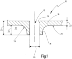
- Fig. 1 shows a plate element 10.
- a section of the plate element is shown around a recess 12.
- the plate element 10 has at least one recess, but in particular a plurality of recesses.
- the recess has an inner surface 14.
- the recess has a circular cross-section, but in principle any cross-sectional shape can be provided.
- the recess is surrounded by a collar portion 16 on one side 21 of the plate element 10.
- the recess 12 extends through a plate body 18 of the plate element 10 and the collar portion 16.
- the collar section extends on the side 21 from a surface 20 of the plate body 18. It thus protrudes from the plate surface 20 by a collar section height 25.
- a thickness of the plate body 18 of the plate element 10 is identified by the reference numeral 22.
- a depth of the recess 12 is identified by the reference numeral 24.
- a diameter of the recess is identified by the reference numeral 26.
- a collar section height 25 designates the amount by which the collar section 16 protrudes from the surface 20.
- a thickness 22 of the plate body 18 can be approximately 0.8 mm.
- the collar section height 25 can be 1.2 mm.
- the depth 24 of the recess 12 therefore results in a total depth of 2 mm, which is sufficient for a press-fitting process.
- a diameter 26 of the recess 12 can also be 2 mm.
- a surface quality of the plate arrangement can be Ra 0.8.
- a radius 28 with which the collar section 16 merges onto the surface 20 can be 0.2 mm.
- the diameter 26 is 1.45 mm and the total depth 24 is 1.5 mm.
- the depth 24 can be at least 1.5 times the thickness 22.
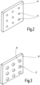
- the Fig. 2 shows an isometric view of an embodiment of a plate element 10. As shown, in principle several recesses 12 can be provided in the plate element 10.
- each recess 12 has a collar portion 16.
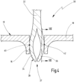
- the Fig. 4 shows an embodiment of a component arrangement 30.
- a contact element 32 is pressed into the recess 12 so that it contacts the Fig. 4
- the contact element 32 has two leg sections 34, 36, which come into contact with the inner surface 14 at least at contact points 40, 42 when pressed in.
- the leg sections 34, 36 are arranged at one end 37 of the contact element 32.
- the leg sections 34, 36 have a surface 38.
- the surface can be tinned.
- the inner surface 14 and the leg sections 34, 36 can also be uncoated.
- For a material both for the leg sections 34, 36 or for the entire contact element 32 can be made of copper.
- the plate element 10 can also be made of copper.
- Fig. 5 shows a top view of the recess 12. One looks at one end 44 of the leg sections 34, 36. A side surface 39 of the leg sections 34, 36 can be formed straight, so that approximately the Fig. 5 visible contact of the leg sections 34, 36 with the inner surface 14. As can be seen, a cross section of the leg sections 34, 36 can be designed such that two contact points 40, 40' or 42, 42' are obtained for each leg section. In this way, a stable 4-point contact can be provided.
- FIG. 6 A further embodiment is shown. It can also be provided in principle that the side surfaces 39 are each designed with a curvature 46. In this way, the leg sections 34, 36 can also come into contact with the inner surface 14 laterally and thus provide further contact points.
- leg sections 48, 50 can be provided, namely further leg sections 48, 50.
- the contact element can thus also have, for example, three or four leg sections in order to provide more contact points to the inner surface 14 than is possible with two leg sections 34, 36.
- Fig. 8 is a schematic view along a line XIII-XIII, as for example in the embodiment in Fig. 6 would be designed. From the Fig. 8 The design of the side surface 39 of the leg sections is thus visible. As already described above, the side surfaces 39 have curvatures 46. This results in additional contact points 52, 54 to the inner surface 14 of the recesses.
- FIG. 9 A further embodiment of a contact element 32 is shown.
- the contact element has two opposite ends 74 and 76 each has at least two leg sections 34, 36 or 34', 36'. This makes it possible to arrange two plate elements 10 opposite one another on a connecting body 32.
- a group 80 of several contact elements 32, 32', 32", 32" is shown. These are connected to one another by means of a rail section. If, for example, high electrical currents, such as 200 A, are to be absorbed, a rail section 78 with four contact elements 32, 32', 32", 32" can be used. Each contact element 32, 32', 32", 32 can be provided with two branch sections 34, 36.
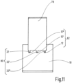
- a further embodiment of a component arrangement 30 is shown.
- the group 80 of several contact elements 32, 32', 32" is pressed into a group 82 of a corresponding number of recesses 12, 12', 12"
- a multiple press-in connection is formed.
- Each contact element 32, 32', 32" adapts to each recess 12 and each collar section 16 by deforming.
- a high-current connection is created between the plate element 10 and the rail section 78.
- the increased contact lengths of the collar sections make it possible to conduct very high currents.
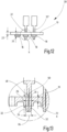
- Fig. 12 and 13 shows a further embodiment of a component arrangement 30 is shown.
- Fig. 13 shows a detailed view X in the Fig. 12 .
- a plurality of contact elements 32, 32' which are formed separately from one another, are connected to the plate element 10.
- the collar sections 16 are formed in such a way that open collar sections 16 with an inner diameter 26 and the thickness 22 of the plate element 10 are formed from the plate element 10 by tensile pressure forming.
- the depth 24 is approximately twice as long as the thickness 22, i.e. 24 can be 1.8 times to 2.5 times as long as the thickness 22.
- a contact element 32 has two opposing bent leg sections 34, 36, which leave a leg gap 35 between them.
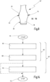
- FIG. 14 schematic flow diagrams of a non-claimed method 60 for producing a plate element and of a non-claimed method 62 for producing a component arrangement are shown.
- the method 60 for producing a plate element begins in a start step 64, wherein a plate element is first provided in a step 66.
- the collar sections 16 and the recesses 12 are then provided in the plate element 10 by deep drawing.
- the recesses 12, in particular with a smaller diameter can also be provided before deep drawing, for example when casting the plate element or by being introduced in advance in another way.
- the collar sections 16 are formed by deep drawing. This method then ends in a stop step 72. In principle, after deep drawing, it can be provided to tin the inner surface 14 of the recesses 12.
- the steps 64, 66, 68 and, if necessary, tinning are also carried out first.
- a contact element with at least two leg sections described above is provided. This contact element is pressed into one of the at least one recesses 12 with the leg sections 34, 36 or additionally 48, 50.
- the pressing-in process 70 can be repeated and thus a plurality of contact elements can be pressed into one recess each. In this way, it can be provided, for example, that as in the Fig. 2 and 3 shown, nine recesses are provided and nine contact elements are pressed in, one contact element in each recess.
- the contact element 32 is connected to the respective recess 12 and the associated collar section 16, for example with a stroke of approximately 0.1 seconds. Due to the fact that an inner diameter 26 is smaller than an outer diameter 84 of the branch sections 34, 36 of the contact element 32, a very high pressing pressure is created, which leads to a welding of the materials of the contact element 32 and the plate element 10 without the influence of temperature. A direct, elastic connection with a very high specific electrical conductivity is created. Because a contact surface has been enlarged due to a collar section 16, currents of, for example, 20 A and more can be passed on in a 12 V vehicle electrical system.
- the method for producing a component arrangement then also ends in a stop step 72.
Landscapes
- Engineering & Computer Science (AREA)
- Manufacturing & Machinery (AREA)
- Manufacturing Of Electrical Connectors (AREA)
Claims (6)
- Ensemble de composants (30) pour le guidage de courant, comportantplusieurs éléments formant contacts enfichables (32) qui présentent respectivement au moins deux sections formant branches (34, 36, 48, 50) au niveau d'au moins une extrémité (37) et chaque section formant branche (34, 36, 48, 50) présente des surfaces latérales (39) bombées vers l'extérieur, dans lequel les éléments formant contacts enfichables (32) sont reliés entre eux par l'intermédiaire d'une section formant rail (78) ; etun élément formant plaque (10) pour le guidage de courant, lequel élément formant plaque présente une épaisseur (22) et plusieurs évidements (12) circulaires pour la fourniture d'un logement pour contact pour un élément formant contact enfichable (32), dans lequel chaque évidement (12) est entouré par une section formant collerette (16) sur au moins un côté (21) de l'élément formant plaque ;dans lequelles au moins deux sections formant branches (34, 36, 48, 50) sont enfichées dans respectivement un évidement (12) et sont respectivement en contact avec une surface intérieure (14) de l'évidement (12) respectif, dans lequel un sommet (52, 54) respectif d'une courbure (46) est en contact avec la surface intérieure (14) ;les évidements et les sections formant collerettes sont fournis par emboutissage ;l'épaisseur de l'élément formant plaque est d'environ 0,8 mm, etles sections formant collerettes (16) s'étendent à partir d'une surface (20) de l'élément formant plaque (10) et comportent une hauteur de section formant collerette (25) qui se situe dans la plage allant de 0,4 mm à 1,6 mm.
- Ensemble de composants selon la revendication 1, caractérisé en ce que la section formant collerette (16) se prolonge avec un rayon (28) sur une surface (20) de l'élément formant plaque (10).
- Ensemble de composants selon l'une des revendications 1 à 2, caractérisé en ce que les évidements (12) sont réalisés respectivement sous forme d'un trou de passage traversant l'élément formant plaque (10) et la section formant collerette (16).
- Ensemble de composants selon l'une des revendications 1 à 3, caractérisé en ce que la surface intérieure (14) des évidements (12) est revêtue d'étain.
- Ensemble de composants selon la revendication 1, caractérisé en ce qu'au moins les au moins deux sections formant branches (34, 36, 48, 50) de l'élément formant contact (32) sont réalisées en cuivre.
- Ensemble de composants selon la revendication 1 ou 5,
caractérisé en ce qu'une surface (38) des au moins deux sections formant branches (34, 36, 48, 50) est revêtue d'étain.
Applications Claiming Priority (3)
| Application Number | Priority Date | Filing Date | Title |
|---|---|---|---|
| DE102012022531 | 2012-11-14 | ||
| DE102013111963.8A DE102013111963A1 (de) | 2012-11-14 | 2013-10-30 | Plattenelement mit Tiefziehbohrung für Einpresskontakte |
| PCT/EP2013/073704 WO2014076122A1 (fr) | 2012-11-14 | 2013-11-13 | Élément carte pourvu d'un alésage embouti pour contacts à encastrer |
Publications (2)
| Publication Number | Publication Date |
|---|---|
| EP2920847A1 EP2920847A1 (fr) | 2015-09-23 |
| EP2920847B1 true EP2920847B1 (fr) | 2024-10-16 |
Family
ID=50555961
Family Applications (1)
| Application Number | Title | Priority Date | Filing Date |
|---|---|---|---|
| EP13791798.5A Active EP2920847B1 (fr) | 2012-11-14 | 2013-11-13 | Élément carte pourvu d'un alésage embouti pour contacts à encastrer |
Country Status (3)
| Country | Link |
|---|---|
| EP (1) | EP2920847B1 (fr) |
| DE (1) | DE102013111963A1 (fr) |
| WO (1) | WO2014076122A1 (fr) |
Families Citing this family (6)
| Publication number | Priority date | Publication date | Assignee | Title |
|---|---|---|---|---|
| DE102014117410B4 (de) * | 2014-11-27 | 2019-01-03 | Heraeus Deutschland GmbH & Co. KG | Elektrisches Kontaktelement, Einpressstift, Buchse und Leadframe |
| DE102015100149A1 (de) | 2015-01-08 | 2016-07-14 | Raimund Huber | Elektrisches Funktionsbauteil mit Kontaktstift und Verfahren zur Herstellung eines elektrischen Funktionsbauteils |
| EP3016208B1 (fr) * | 2015-08-24 | 2019-11-20 | Continental Teves AG & Co. OHG | Dispositif électrique comprenant un agencement de contact et procédé de fabrication d'un encadrement d'un agencement de contact. |
| DE102015119785B4 (de) | 2015-11-04 | 2020-03-26 | ept Holding GmbH & Co. KG | Lochkontur für Einpresstechnik in ein Stanzgitter |
| DE102016115173A1 (de) * | 2016-08-16 | 2018-02-22 | Abb Schweiz Ag | Dünner Leiter mit Durchgängen |
| DE102022134501A1 (de) * | 2022-12-22 | 2024-06-27 | Te Connectivity Solutions Gmbh | Gehäuseelement für eine elektronische Schaltung |
Citations (4)
| Publication number | Priority date | Publication date | Assignee | Title |
|---|---|---|---|---|
| EP1391965A1 (fr) * | 2002-08-22 | 2004-02-25 | Wago Verwaltungsgesellschaft mbH | Borne à ressort pour conducteur électrique |
| US20050204538A1 (en) * | 2004-03-19 | 2005-09-22 | Epic Technology Inc. | Contact and method for making same |
| US20080166928A1 (en) * | 2007-01-10 | 2008-07-10 | Liang Tang | Compliant pin |
| US20130143433A1 (en) * | 2010-08-09 | 2013-06-06 | Phoenix Contact Gmbh & Co. Kg | Connection terminal |
Family Cites Families (3)
| Publication number | Priority date | Publication date | Assignee | Title |
|---|---|---|---|---|
| DE102004006533A1 (de) | 2004-02-11 | 2005-09-01 | Conti Temic Microelectronic Gmbh | Elektrisch leitfähiger Kontaktstift zum Einpressen in eine Öffnung einer Leiterplatte sowie elektrische Baugruppe mit einem solchen Kontaktstift |
| DE102004006575A1 (de) | 2004-02-11 | 2005-09-01 | Leopold Kostal Gmbh & Co Kg | Leistungsverteiler für ein Kraftfahrzeug |
| DE102008024366B4 (de) * | 2008-05-20 | 2010-11-25 | Phoenix Contact Gmbh & Co. Kg | Durchführungsklemme |
-
2013
- 2013-10-30 DE DE102013111963.8A patent/DE102013111963A1/de active Pending
- 2013-11-13 WO PCT/EP2013/073704 patent/WO2014076122A1/fr not_active Ceased
- 2013-11-13 EP EP13791798.5A patent/EP2920847B1/fr active Active
Patent Citations (4)
| Publication number | Priority date | Publication date | Assignee | Title |
|---|---|---|---|---|
| EP1391965A1 (fr) * | 2002-08-22 | 2004-02-25 | Wago Verwaltungsgesellschaft mbH | Borne à ressort pour conducteur électrique |
| US20050204538A1 (en) * | 2004-03-19 | 2005-09-22 | Epic Technology Inc. | Contact and method for making same |
| US20080166928A1 (en) * | 2007-01-10 | 2008-07-10 | Liang Tang | Compliant pin |
| US20130143433A1 (en) * | 2010-08-09 | 2013-06-06 | Phoenix Contact Gmbh & Co. Kg | Connection terminal |
Also Published As
| Publication number | Publication date |
|---|---|
| DE102013111963A1 (de) | 2014-05-15 |
| EP2920847A1 (fr) | 2015-09-23 |
| WO2014076122A1 (fr) | 2014-05-22 |
Similar Documents
| Publication | Publication Date | Title |
|---|---|---|
| EP2899812B1 (fr) | Système de connexion sur des plaques de circuit imprimé | |
| EP2441129B1 (fr) | Contact à insérer pour relier un composant électronique à une carte de circuits imprimés ainsi qu'outil d'insertion et procédé pour fabriquer un contact à insérer | |
| EP2920847B1 (fr) | Élément carte pourvu d'un alésage embouti pour contacts à encastrer | |
| DE102011122371A1 (de) | Elektrische Anschlusseinrichtung zur Herstellung einer Lötverbindung | |
| EP3477781A1 (fr) | Douille enfichable pour cartes de circuits imprimés | |
| DE102013209407A1 (de) | Verfahren zur lötfreien elektrischen Einpresskontaktierung von elektrisch leitfähigen Einpress-Stiften in Leiterplatten | |
| EP1754285B1 (fr) | Contact d'estampage | |
| EP3022805A1 (fr) | Dispositif de contact pour la réalisation d'une connexion électrique avec le site de contact d'un circuit imprimé | |
| EP3243246B1 (fr) | Composant fonctionnel électrique à broche de contact et procédé de fabrication d'un composant fonctionnel électrique | |
| EP2705578A1 (fr) | Élément de contact électrique | |
| EP3192130B1 (fr) | Procédé de mise en contact électrique par insertion sans soudure de broches électriquement conductrices à insérer dans des cartes de circuits imprimés | |
| DE102013013368B4 (de) | Verfahren zur Herstellung einer elektrischen Verbindung sowie elektrische Verbindung | |
| DE102012218433B4 (de) | Kontaktanordnung | |
| EP2700126A2 (fr) | Élément de contact à courant fort pour circuits imprimés | |
| EP2732508B1 (fr) | Elemnent connecteur directe avec verrouillage | |
| EP1912295A1 (fr) | Barre omnibus | |
| DE102006011262A1 (de) | Elektrischer Verbinder und Verfahren zu dessen Herstellung | |
| EP2109186B1 (fr) | Procédé de fabrication d'une connexion électrique entre un rail conducteur et une circuit imprimé | |
| DE102004041169B3 (de) | Anordnung und Verfahren zur Masseanbindung eines elektrischen Schaltungsträgers | |
| EP1363362A1 (fr) | Formage des fils électriques d'un câble plat | |
| DE102006000958B4 (de) | Elektrisches Gerät | |
| EP1162694B1 (fr) | Appareil pour la connexion de conducteurs électriques | |
| WO2009003907A1 (fr) | Connecteur | |
| DE102016116375B4 (de) | Kontaktierungsvorrichtung | |
| DE102013201689A1 (de) | Schirmgehäuse |
Legal Events
| Date | Code | Title | Description |
|---|---|---|---|
| PUAI | Public reference made under article 153(3) epc to a published international application that has entered the european phase |
Free format text: ORIGINAL CODE: 0009012 |
|
| 17P | Request for examination filed |
Effective date: 20150611 |
|
| AK | Designated contracting states |
Kind code of ref document: A1 Designated state(s): AL AT BE BG CH CY CZ DE DK EE ES FI FR GB GR HR HU IE IS IT LI LT LU LV MC MK MT NL NO PL PT RO RS SE SI SK SM TR |
|
| AX | Request for extension of the european patent |
Extension state: BA ME |
|
| DAX | Request for extension of the european patent (deleted) | ||
| STAA | Information on the status of an ep patent application or granted ep patent |
Free format text: STATUS: EXAMINATION IS IN PROGRESS |
|
| 17Q | First examination report despatched |
Effective date: 20170926 |
|
| RAP3 | Party data changed (applicant data changed or rights of an application transferred) |
Owner name: IWIS MECHATRONICS GMBH & CO. KG |
|
| P01 | Opt-out of the competence of the unified patent court (upc) registered |
Effective date: 20230724 |
|
| GRAP | Despatch of communication of intention to grant a patent |
Free format text: ORIGINAL CODE: EPIDOSNIGR1 |
|
| STAA | Information on the status of an ep patent application or granted ep patent |
Free format text: STATUS: GRANT OF PATENT IS INTENDED |
|
| INTG | Intention to grant announced |
Effective date: 20240513 |
|
| GRAS | Grant fee paid |
Free format text: ORIGINAL CODE: EPIDOSNIGR3 |
|
| GRAA | (expected) grant |
Free format text: ORIGINAL CODE: 0009210 |
|
| STAA | Information on the status of an ep patent application or granted ep patent |
Free format text: STATUS: THE PATENT HAS BEEN GRANTED |
|
| AK | Designated contracting states |
Kind code of ref document: B1 Designated state(s): AL AT BE BG CH CY CZ DE DK EE ES FI FR GB GR HR HU IE IS IT LI LT LU LV MC MK MT NL NO PL PT RO RS SE SI SK SM TR |
|
| REG | Reference to a national code |
Ref country code: GB Ref legal event code: FG4D Free format text: NOT ENGLISH |
|
| REG | Reference to a national code |
Ref country code: DE Ref legal event code: R096 Ref document number: 502013016548 Country of ref document: DE Ref country code: CH Ref legal event code: EP |
|
| REG | Reference to a national code |
Ref country code: IE Ref legal event code: FG4D Free format text: LANGUAGE OF EP DOCUMENT: GERMAN |
|
| REG | Reference to a national code |
Ref country code: LT Ref legal event code: MG9D |
|
| REG | Reference to a national code |
Ref country code: NL Ref legal event code: MP Effective date: 20241016 |
|
| PG25 | Lapsed in a contracting state [announced via postgrant information from national office to epo] |
Ref country code: NL Free format text: LAPSE BECAUSE OF FAILURE TO SUBMIT A TRANSLATION OF THE DESCRIPTION OR TO PAY THE FEE WITHIN THE PRESCRIBED TIME-LIMIT Effective date: 20241016 |
|
| PG25 | Lapsed in a contracting state [announced via postgrant information from national office to epo] |
Ref country code: NL Free format text: LAPSE BECAUSE OF FAILURE TO SUBMIT A TRANSLATION OF THE DESCRIPTION OR TO PAY THE FEE WITHIN THE PRESCRIBED TIME-LIMIT Effective date: 20241016 |
|
| PG25 | Lapsed in a contracting state [announced via postgrant information from national office to epo] |
Ref country code: IS Free format text: LAPSE BECAUSE OF FAILURE TO SUBMIT A TRANSLATION OF THE DESCRIPTION OR TO PAY THE FEE WITHIN THE PRESCRIBED TIME-LIMIT Effective date: 20250216 Ref country code: PT Free format text: LAPSE BECAUSE OF FAILURE TO SUBMIT A TRANSLATION OF THE DESCRIPTION OR TO PAY THE FEE WITHIN THE PRESCRIBED TIME-LIMIT Effective date: 20250217 Ref country code: HR Free format text: LAPSE BECAUSE OF FAILURE TO SUBMIT A TRANSLATION OF THE DESCRIPTION OR TO PAY THE FEE WITHIN THE PRESCRIBED TIME-LIMIT Effective date: 20241016 |
|
| PG25 | Lapsed in a contracting state [announced via postgrant information from national office to epo] |
Ref country code: FI Free format text: LAPSE BECAUSE OF FAILURE TO SUBMIT A TRANSLATION OF THE DESCRIPTION OR TO PAY THE FEE WITHIN THE PRESCRIBED TIME-LIMIT Effective date: 20241016 |
|
| PG25 | Lapsed in a contracting state [announced via postgrant information from national office to epo] |
Ref country code: BG Free format text: LAPSE BECAUSE OF FAILURE TO SUBMIT A TRANSLATION OF THE DESCRIPTION OR TO PAY THE FEE WITHIN THE PRESCRIBED TIME-LIMIT Effective date: 20241016 |
|
| PG25 | Lapsed in a contracting state [announced via postgrant information from national office to epo] |
Ref country code: ES Free format text: LAPSE BECAUSE OF FAILURE TO SUBMIT A TRANSLATION OF THE DESCRIPTION OR TO PAY THE FEE WITHIN THE PRESCRIBED TIME-LIMIT Effective date: 20241016 |
|
| PG25 | Lapsed in a contracting state [announced via postgrant information from national office to epo] |
Ref country code: NO Free format text: LAPSE BECAUSE OF FAILURE TO SUBMIT A TRANSLATION OF THE DESCRIPTION OR TO PAY THE FEE WITHIN THE PRESCRIBED TIME-LIMIT Effective date: 20250116 |
|
| PG25 | Lapsed in a contracting state [announced via postgrant information from national office to epo] |
Ref country code: GR Free format text: LAPSE BECAUSE OF FAILURE TO SUBMIT A TRANSLATION OF THE DESCRIPTION OR TO PAY THE FEE WITHIN THE PRESCRIBED TIME-LIMIT Effective date: 20250117 Ref country code: LV Free format text: LAPSE BECAUSE OF FAILURE TO SUBMIT A TRANSLATION OF THE DESCRIPTION OR TO PAY THE FEE WITHIN THE PRESCRIBED TIME-LIMIT Effective date: 20241016 |
|
| PG25 | Lapsed in a contracting state [announced via postgrant information from national office to epo] |
Ref country code: PL Free format text: LAPSE BECAUSE OF FAILURE TO SUBMIT A TRANSLATION OF THE DESCRIPTION OR TO PAY THE FEE WITHIN THE PRESCRIBED TIME-LIMIT Effective date: 20241016 |
|
| PG25 | Lapsed in a contracting state [announced via postgrant information from national office to epo] |
Ref country code: RS Free format text: LAPSE BECAUSE OF FAILURE TO SUBMIT A TRANSLATION OF THE DESCRIPTION OR TO PAY THE FEE WITHIN THE PRESCRIBED TIME-LIMIT Effective date: 20250116 |
|
| REG | Reference to a national code |
Ref country code: CH Ref legal event code: PL |
|
| PG25 | Lapsed in a contracting state [announced via postgrant information from national office to epo] |
Ref country code: SM Free format text: LAPSE BECAUSE OF FAILURE TO SUBMIT A TRANSLATION OF THE DESCRIPTION OR TO PAY THE FEE WITHIN THE PRESCRIBED TIME-LIMIT Effective date: 20241016 |
|
| PG25 | Lapsed in a contracting state [announced via postgrant information from national office to epo] |
Ref country code: MC Free format text: LAPSE BECAUSE OF FAILURE TO SUBMIT A TRANSLATION OF THE DESCRIPTION OR TO PAY THE FEE WITHIN THE PRESCRIBED TIME-LIMIT Effective date: 20241016 |
|
| PG25 | Lapsed in a contracting state [announced via postgrant information from national office to epo] |
Ref country code: DK Free format text: LAPSE BECAUSE OF FAILURE TO SUBMIT A TRANSLATION OF THE DESCRIPTION OR TO PAY THE FEE WITHIN THE PRESCRIBED TIME-LIMIT Effective date: 20241016 |
|
| PG25 | Lapsed in a contracting state [announced via postgrant information from national office to epo] |
Ref country code: LU Free format text: LAPSE BECAUSE OF NON-PAYMENT OF DUE FEES Effective date: 20241113 |
|
| REG | Reference to a national code |
Ref country code: CH Ref legal event code: PL |
|
| REG | Reference to a national code |
Ref country code: DE Ref legal event code: R097 Ref document number: 502013016548 Country of ref document: DE |
|
| PG25 | Lapsed in a contracting state [announced via postgrant information from national office to epo] |
Ref country code: EE Free format text: LAPSE BECAUSE OF FAILURE TO SUBMIT A TRANSLATION OF THE DESCRIPTION OR TO PAY THE FEE WITHIN THE PRESCRIBED TIME-LIMIT Effective date: 20241016 |
|
| PG25 | Lapsed in a contracting state [announced via postgrant information from national office to epo] |
Ref country code: CH Free format text: LAPSE BECAUSE OF NON-PAYMENT OF DUE FEES Effective date: 20241130 |
|
| PG25 | Lapsed in a contracting state [announced via postgrant information from national office to epo] |
Ref country code: RO Free format text: LAPSE BECAUSE OF FAILURE TO SUBMIT A TRANSLATION OF THE DESCRIPTION OR TO PAY THE FEE WITHIN THE PRESCRIBED TIME-LIMIT Effective date: 20241016 |
|
| PG25 | Lapsed in a contracting state [announced via postgrant information from national office to epo] |
Ref country code: SK Free format text: LAPSE BECAUSE OF FAILURE TO SUBMIT A TRANSLATION OF THE DESCRIPTION OR TO PAY THE FEE WITHIN THE PRESCRIBED TIME-LIMIT Effective date: 20241016 |
|
| PG25 | Lapsed in a contracting state [announced via postgrant information from national office to epo] |
Ref country code: CZ Free format text: LAPSE BECAUSE OF FAILURE TO SUBMIT A TRANSLATION OF THE DESCRIPTION OR TO PAY THE FEE WITHIN THE PRESCRIBED TIME-LIMIT Effective date: 20241016 |
|
| PG25 | Lapsed in a contracting state [announced via postgrant information from national office to epo] |
Ref country code: IT Free format text: LAPSE BECAUSE OF FAILURE TO SUBMIT A TRANSLATION OF THE DESCRIPTION OR TO PAY THE FEE WITHIN THE PRESCRIBED TIME-LIMIT Effective date: 20241016 |
|
| PLBE | No opposition filed within time limit |
Free format text: ORIGINAL CODE: 0009261 |
|
| STAA | Information on the status of an ep patent application or granted ep patent |
Free format text: STATUS: NO OPPOSITION FILED WITHIN TIME LIMIT |
|
| REG | Reference to a national code |
Ref country code: BE Ref legal event code: MM Effective date: 20241130 |
|
| PG25 | Lapsed in a contracting state [announced via postgrant information from national office to epo] |
Ref country code: SE Free format text: LAPSE BECAUSE OF FAILURE TO SUBMIT A TRANSLATION OF THE DESCRIPTION OR TO PAY THE FEE WITHIN THE PRESCRIBED TIME-LIMIT Effective date: 20241016 |
|
| 26N | No opposition filed |
Effective date: 20250717 |
|
| GBPC | Gb: european patent ceased through non-payment of renewal fee |
Effective date: 20250116 |
|
| PG25 | Lapsed in a contracting state [announced via postgrant information from national office to epo] |
Ref country code: BE Free format text: LAPSE BECAUSE OF NON-PAYMENT OF DUE FEES Effective date: 20241130 Ref country code: GB Free format text: LAPSE BECAUSE OF NON-PAYMENT OF DUE FEES Effective date: 20250116 |
|
| REG | Reference to a national code |
Ref country code: DE Ref legal event code: R082 Ref document number: 502013016548 Country of ref document: DE Representative=s name: PATENTANWAELTE BREGENZER UND REULE PARTNERSCHA, DE |
|
| PG25 | Lapsed in a contracting state [announced via postgrant information from national office to epo] |
Ref country code: FR Free format text: LAPSE BECAUSE OF NON-PAYMENT OF DUE FEES Effective date: 20241216 |
|
| PG25 | Lapsed in a contracting state [announced via postgrant information from national office to epo] |
Ref country code: IE Free format text: LAPSE BECAUSE OF NON-PAYMENT OF DUE FEES Effective date: 20241113 |
|
| PGFP | Annual fee paid to national office [announced via postgrant information from national office to epo] |
Ref country code: DE Payment date: 20251118 Year of fee payment: 13 |
|
| PG25 | Lapsed in a contracting state [announced via postgrant information from national office to epo] |
Ref country code: AT Free format text: LAPSE BECAUSE OF NON-PAYMENT OF DUE FEES Effective date: 20241113 |
|
| REG | Reference to a national code |
Ref country code: AT Ref legal event code: MM01 Ref document number: 1733723 Country of ref document: AT Kind code of ref document: T Effective date: 20241113 |
|
| PG25 | Lapsed in a contracting state [announced via postgrant information from national office to epo] |
Ref country code: HU Free format text: LAPSE BECAUSE OF FAILURE TO SUBMIT A TRANSLATION OF THE DESCRIPTION OR TO PAY THE FEE WITHIN THE PRESCRIBED TIME-LIMIT; INVALID AB INITIO Effective date: 20131113 |
|
| PG25 | Lapsed in a contracting state [announced via postgrant information from national office to epo] |
Ref country code: CY Free format text: LAPSE BECAUSE OF FAILURE TO SUBMIT A TRANSLATION OF THE DESCRIPTION OR TO PAY THE FEE WITHIN THE PRESCRIBED TIME-LIMIT; INVALID AB INITIO Effective date: 20131113 |