EP3243246B1 - Composant fonctionnel électrique à broche de contact et procédé de fabrication d'un composant fonctionnel électrique - Google Patents
Composant fonctionnel électrique à broche de contact et procédé de fabrication d'un composant fonctionnel électrique Download PDFInfo
- Publication number
- EP3243246B1 EP3243246B1 EP15817113.2A EP15817113A EP3243246B1 EP 3243246 B1 EP3243246 B1 EP 3243246B1 EP 15817113 A EP15817113 A EP 15817113A EP 3243246 B1 EP3243246 B1 EP 3243246B1
- Authority
- EP
- European Patent Office
- Prior art keywords
- contact pin
- contact
- recess
- functional component
- zone
- Prior art date
- Legal status (The legal status is an assumption and is not a legal conclusion. Google has not performed a legal analysis and makes no representation as to the accuracy of the status listed.)
- Active
Links
Images


Classifications
-
- H—ELECTRICITY
- H01—ELECTRIC ELEMENTS
- H01R—ELECTRICALLY-CONDUCTIVE CONNECTIONS; STRUCTURAL ASSOCIATIONS OF A PLURALITY OF MUTUALLY-INSULATED ELECTRICAL CONNECTING ELEMENTS; COUPLING DEVICES; CURRENT COLLECTORS
- H01R4/00—Electrically-conductive connections between two or more conductive members in direct contact, i.e. touching one another; Means for effecting or maintaining such contact; Electrically-conductive connections having two or more spaced connecting locations for conductors and using contact members penetrating insulation
- H01R4/10—Electrically-conductive connections between two or more conductive members in direct contact, i.e. touching one another; Means for effecting or maintaining such contact; Electrically-conductive connections having two or more spaced connecting locations for conductors and using contact members penetrating insulation effected solely by twisting, wrapping, bending, crimping, or other permanent deformation
-
- H—ELECTRICITY
- H01—ELECTRIC ELEMENTS
- H01R—ELECTRICALLY-CONDUCTIVE CONNECTIONS; STRUCTURAL ASSOCIATIONS OF A PLURALITY OF MUTUALLY-INSULATED ELECTRICAL CONNECTING ELEMENTS; COUPLING DEVICES; CURRENT COLLECTORS
- H01R43/00—Apparatus or processes specially adapted for manufacturing, assembling, maintaining, or repairing of line connectors or current collectors or for joining electric conductors
- H01R43/16—Apparatus or processes specially adapted for manufacturing, assembling, maintaining, or repairing of line connectors or current collectors or for joining electric conductors for manufacturing contact members, e.g. by punching and by bending
-
- B—PERFORMING OPERATIONS; TRANSPORTING
- B23—MACHINE TOOLS; METAL-WORKING NOT OTHERWISE PROVIDED FOR
- B23K—SOLDERING OR UNSOLDERING; WELDING; CLADDING OR PLATING BY SOLDERING OR WELDING; CUTTING BY APPLYING HEAT LOCALLY, e.g. FLAME CUTTING; WORKING BY LASER BEAM
- B23K20/00—Non-electric welding by applying impact or other pressure, with or without the application of heat, e.g. cladding or plating
- B23K20/02—Non-electric welding by applying impact or other pressure, with or without the application of heat, e.g. cladding or plating by means of a press ; Diffusion bonding
-
- B—PERFORMING OPERATIONS; TRANSPORTING
- B23—MACHINE TOOLS; METAL-WORKING NOT OTHERWISE PROVIDED FOR
- B23K—SOLDERING OR UNSOLDERING; WELDING; CLADDING OR PLATING BY SOLDERING OR WELDING; CUTTING BY APPLYING HEAT LOCALLY, e.g. FLAME CUTTING; WORKING BY LASER BEAM
- B23K20/00—Non-electric welding by applying impact or other pressure, with or without the application of heat, e.g. cladding or plating
- B23K20/22—Non-electric welding by applying impact or other pressure, with or without the application of heat, e.g. cladding or plating taking account of the properties of the materials to be welded
-
- H—ELECTRICITY
- H01—ELECTRIC ELEMENTS
- H01B—CABLES; CONDUCTORS; INSULATORS; SELECTION OF MATERIALS FOR THEIR CONDUCTIVE, INSULATING OR DIELECTRIC PROPERTIES
- H01B13/00—Apparatus or processes specially adapted for manufacturing conductors or cables
- H01B13/0036—Details
-
- H—ELECTRICITY
- H01—ELECTRIC ELEMENTS
- H01B—CABLES; CONDUCTORS; INSULATORS; SELECTION OF MATERIALS FOR THEIR CONDUCTIVE, INSULATING OR DIELECTRIC PROPERTIES
- H01B5/00—Non-insulated conductors or conductive bodies characterised by their form
- H01B5/02—Single bars, rods, wires, or strips
-
- H—ELECTRICITY
- H01—ELECTRIC ELEMENTS
- H01R—ELECTRICALLY-CONDUCTIVE CONNECTIONS; STRUCTURAL ASSOCIATIONS OF A PLURALITY OF MUTUALLY-INSULATED ELECTRICAL CONNECTING ELEMENTS; COUPLING DEVICES; CURRENT COLLECTORS
- H01R12/00—Structural associations of a plurality of mutually-insulated electrical connecting elements, specially adapted for printed circuits, e.g. printed circuit boards [PCB], flat or ribbon cables, or like generally planar structures, e.g. terminal strips, terminal blocks; Coupling devices specially adapted for printed circuits, flat or ribbon cables, or like generally planar structures; Terminals specially adapted for contact with, or insertion into, printed circuits, flat or ribbon cables, or like generally planar structures
- H01R12/50—Fixed connections
- H01R12/51—Fixed connections for rigid printed circuits or like structures
- H01R12/55—Fixed connections for rigid printed circuits or like structures characterised by the terminals
- H01R12/58—Fixed connections for rigid printed circuits or like structures characterised by the terminals terminals for insertion into holes
- H01R12/585—Terminals having a press fit or a compliant portion and a shank passing through a hole in the printed circuit board
-
- H—ELECTRICITY
- H01—ELECTRIC ELEMENTS
- H01R—ELECTRICALLY-CONDUCTIVE CONNECTIONS; STRUCTURAL ASSOCIATIONS OF A PLURALITY OF MUTUALLY-INSULATED ELECTRICAL CONNECTING ELEMENTS; COUPLING DEVICES; CURRENT COLLECTORS
- H01R12/00—Structural associations of a plurality of mutually-insulated electrical connecting elements, specially adapted for printed circuits, e.g. printed circuit boards [PCB], flat or ribbon cables, or like generally planar structures, e.g. terminal strips, terminal blocks; Coupling devices specially adapted for printed circuits, flat or ribbon cables, or like generally planar structures; Terminals specially adapted for contact with, or insertion into, printed circuits, flat or ribbon cables, or like generally planar structures
- H01R12/70—Coupling devices
- H01R12/7005—Guiding, mounting, polarizing or locking means; Extractors
- H01R12/7011—Locking or fixing a connector to a PCB
- H01R12/7064—Press fitting
-
- H—ELECTRICITY
- H01—ELECTRIC ELEMENTS
- H01R—ELECTRICALLY-CONDUCTIVE CONNECTIONS; STRUCTURAL ASSOCIATIONS OF A PLURALITY OF MUTUALLY-INSULATED ELECTRICAL CONNECTING ELEMENTS; COUPLING DEVICES; CURRENT COLLECTORS
- H01R13/00—Details of coupling devices of the kinds covered by groups H01R12/70 or H01R24/00 - H01R33/00
- H01R13/02—Contact members
- H01R13/03—Contact members characterised by the material, e.g. plating, or coating materials
-
- H—ELECTRICITY
- H01—ELECTRIC ELEMENTS
- H01R—ELECTRICALLY-CONDUCTIVE CONNECTIONS; STRUCTURAL ASSOCIATIONS OF A PLURALITY OF MUTUALLY-INSULATED ELECTRICAL CONNECTING ELEMENTS; COUPLING DEVICES; CURRENT COLLECTORS
- H01R13/00—Details of coupling devices of the kinds covered by groups H01R12/70 or H01R24/00 - H01R33/00
- H01R13/02—Contact members
- H01R13/04—Pins or blades for co-operation with sockets
-
- H—ELECTRICITY
- H01—ELECTRIC ELEMENTS
- H01R—ELECTRICALLY-CONDUCTIVE CONNECTIONS; STRUCTURAL ASSOCIATIONS OF A PLURALITY OF MUTUALLY-INSULATED ELECTRICAL CONNECTING ELEMENTS; COUPLING DEVICES; CURRENT COLLECTORS
- H01R43/00—Apparatus or processes specially adapted for manufacturing, assembling, maintaining, or repairing of line connectors or current collectors or for joining electric conductors
- H01R43/02—Apparatus or processes specially adapted for manufacturing, assembling, maintaining, or repairing of line connectors or current collectors or for joining electric conductors for soldered or welded connections
- H01R43/0207—Ultrasonic-, H.F.-, cold- or impact welding
-
- H—ELECTRICITY
- H05—ELECTRIC TECHNIQUES NOT OTHERWISE PROVIDED FOR
- H05K—PRINTED CIRCUITS; CASINGS OR CONSTRUCTIONAL DETAILS OF ELECTRIC APPARATUS; MANUFACTURE OF ASSEMBLAGES OF ELECTRICAL COMPONENTS
- H05K1/00—Printed circuits
- H05K1/02—Details
-
- B—PERFORMING OPERATIONS; TRANSPORTING
- B23—MACHINE TOOLS; METAL-WORKING NOT OTHERWISE PROVIDED FOR
- B23K—SOLDERING OR UNSOLDERING; WELDING; CLADDING OR PLATING BY SOLDERING OR WELDING; CUTTING BY APPLYING HEAT LOCALLY, e.g. FLAME CUTTING; WORKING BY LASER BEAM
- B23K2101/00—Articles made by soldering, welding or cutting
- B23K2101/34—Coated articles ; Surface treated articles
-
- B—PERFORMING OPERATIONS; TRANSPORTING
- B23—MACHINE TOOLS; METAL-WORKING NOT OTHERWISE PROVIDED FOR
- B23K—SOLDERING OR UNSOLDERING; WELDING; CLADDING OR PLATING BY SOLDERING OR WELDING; CUTTING BY APPLYING HEAT LOCALLY, e.g. FLAME CUTTING; WORKING BY LASER BEAM
- B23K2101/00—Articles made by soldering, welding or cutting
- B23K2101/36—Electric or electronic devices
- B23K2101/38—Conductors
-
- H—ELECTRICITY
- H01—ELECTRIC ELEMENTS
- H01R—ELECTRICALLY-CONDUCTIVE CONNECTIONS; STRUCTURAL ASSOCIATIONS OF A PLURALITY OF MUTUALLY-INSULATED ELECTRICAL CONNECTING ELEMENTS; COUPLING DEVICES; CURRENT COLLECTORS
- H01R4/00—Electrically-conductive connections between two or more conductive members in direct contact, i.e. touching one another; Means for effecting or maintaining such contact; Electrically-conductive connections having two or more spaced connecting locations for conductors and using contact members penetrating insulation
- H01R4/58—Electrically-conductive connections between two or more conductive members in direct contact, i.e. touching one another; Means for effecting or maintaining such contact; Electrically-conductive connections having two or more spaced connecting locations for conductors and using contact members penetrating insulation characterised by the form or material of the contacting members
- H01R4/60—Connections between or with tubular conductors
Definitions
- the invention relates to an electrical functional component with at least one conductor track, to which a contact pin is attached in an electrically conductive manner, according to the preamble of claim 1.
- the invention further relates to a method for producing an electrical functional component.
- Generic electrical functional components are characterized in that at least one electrically conductive conductor track is provided on the functional component. At least one contact pin is attached to this conductor track.
- the contact pin has the task of contacting the conductor track of the functional component preferably in a detachable manner with a functionally complementary contact element.
- the functionally complementary contact element can be, for example, plug elements in a plug or a socket.
- the electrical functional component itself is designed, for example, in the manner of a plug or illuminant.
- Generic electrical functional components are also known which are designed in the manner of printed circuit boards. Serve on these circuit boards the contact pins of the contacting of the circuit board, for example on plugs or power strips.
- a contact zone is provided between the conductor track and the contact pin, which connects the conductor track and the contact pin in an electrically conductive manner.
- the contact zone between the conductor track and the contact pin represents a potential source of error for the function of the functional component if the contact quality of the contact zone falls below a certain level.
- the true metallic contact surface is of crucial importance for the contact quality.
- contact surfaces age over time and the electrical resistance increases over time. Due to the age-related increase in resistance, the contact zones can even be completely destroyed.
- This mechanism is influenced by different aging mechanisms (chemical reactions, electromigration, interdiffusion, friction wear and force reduction) that take place simultaneously in the contact zones.
- one or more of these mechanisms can accelerate the aging of the contact zone.
- the degradation of force and the chemical reactions through oxidation and relaxation can decisively accelerate aging due to high operating temperatures.
- the pressure force between the contact surfaces can decrease sharply within a few weeks due to dynamic recovery processes, creeping or changes in the mechanical properties of the conductor material. This means that the contact resistance can increase significantly with low connection forces, based on the initial values after the connection has been installed, and thus cause malfunctions in spite of checking the components.
- connection techniques for establishing a contact zone between the conductor track and the contact pin are screwing, welding and riveting. Less frequently, a soldered connection is also used.
- the electrical connection In the case of a screw connection, the electrical connection is only secondary and to a relatively small extent via the screwable connecting element used. In contrast, the electrical connection occurs primarily via the contact surfaces generated by the screw connection, in which the material of the conductor track and the material of the contact pin are pressed against one another by pressing the screw element. The roughness of the component surfaces and the existing oxidation layers on the contact surfaces play a role in the contact quality. The contact quality of such screw connections on generic electrical functional components is therefore relatively low and has a high degree of scatter. It is also a disadvantage of such screw connections that a relatively large number of individual parts must be provided, the assembly of which is complex. In the case of cyclic mechanical loads, a subsequent service interval is also necessary to reliably maintain the necessary pressure between the contact surfaces.
- contact pins When using riveting methods for contacting the contact pin with the conductor track, contact pins can be used, for example, on the shaft of which a contact rivet is formed.
- This contact rivet has a collar for support in the edge region of a recess in the conductor track.
- the contact rivet is equipped with a rivet head which is folded over on the opposite side of the recess in the conductor track and thereby realizes a frictional connection between the contact pin and the conductor track.
- This contact closure causes an axially directed pressing force between the end face of the collar and the inner end face of the rivet head on the one hand and the opposite surface areas of the conductor track on the other hand.
- soldering methods have the disadvantage that relatively complex processing is necessary.
- the supply of the solder material often leads to chemical reactions of the contact partners, which cause the contact point to age.
- the US 3,718,750 A. describes a contact pin for through-plating two circuit boards.
- the contact pin has a corrugation on its circumference.
- the conductor tracks of the printed circuit board each having two sleeve-shaped end pieces which are arranged in the recess.
- a cold-welded contact zone is formed.
- the functional component according to the invention the electrically conductive contact zone between the conductor track and the contact pin being designed in the manner of an annular, cold-pressure-welded transition zone, is characterized in that the recess receiving the contact pin has a conical section-shaped cross section, the recess narrowing in the joining direction of the contact pin.
- the joining pressure is to be selected so high that at least one cold-welded welding zone is created on or in at least one cold-forming zone, in which the contact pin and the conductor track are connected to one another in an electrically conductive manner. Since the contact zone is annular, the formation of the cold forming zone and the welding zone can be achieved in a simple manner in that the outer circumference of the contact pin and the inner circumference of the recess or recess have a material overlap. When the contact pin is pressed into the recess or depression, this overlap ensures that the two components in their superficial material layers are pressed against one another with high pressure and moved past one another. The deformations that occur in the crystal lattice of the joining partners involved ensure a cohesive connection, at least in some areas.
- the tolerance compensation is simplified with regard to the material coverage between the contact pin and the conductor track in that the contact pin has a cross-sectional constriction, namely a conical section-shaped cross section, at at least one end. Due to the narrowing cross section of the contact pin in the press-in direction, the contact pin can also be very easily placed and centered in the recess or depression. With increasing press-in depth, the material coverage is so high that the effect according to the invention of forming a cold-press-welded transition zone is then formed by appropriate cold forming.
- both joining partners have a cold-forming zone in their superficial material layers, these cold-forming zones enclosing the welding zone arranged in between in a layered manner.
- the necessary degree of material coverage between the two joining partners can be determined by simple tests using micrographs of the contact zone.
- the material coverage may only be so large that a macroscopic deformation of the two joining partners by the joining process is excluded.
- the material coverage must be so large that a cold-welded welding zone with a cohesive connection between the two joining partners is formed, at least in regions, by pressing the contact pin into the recess or recess. This can be checked in a simple manner by checking the press-in force in the ongoing production or preparation of micrographs and testing the pull-out force in the form of random testing.
- the functional component according to the invention has the advantage over the known prior art that a mechanically highly resilient connection between the two joining partners on the one hand and an electrical contact zone with high electrical line quality can be produced in one step. A macroscopic heat input into the material does not occur, so that undesirable distortion effects are excluded. In addition, joining partners with almost any material properties can be joined together mechanically and electrically.
- the cold-welded contact zone is not subject to crevice corrosion and a drop in line quality in the contact zone over a longer period of time is almost impossible.
- the design of the conductor track is basically as long as the conductor track has sufficient mechanical stability to press the contact pin into the recess or recess.
- the conductor track can also be a solid metallic component, as is known, for example, for producing plug contacts on lamps.
- the invention has particularly great advantages if the conductor track is designed in the manner of a conductor plate, in particular in the manner of a lead frame. Highly filigree conductor tracks can be provided on such conductor plates, which can be produced inexpensively in particular by punching out.
- the cold forming to form the cold welding zone also means that the contact pins are mechanically connected to the printed circuit board with high strength and thus achieve high maximum extraction forces.
- the mechanical strength of the connection between the contact pin and the conductor track and the electrical line quality between the contact pin and the conductor track were significantly influenced by the size of the annular, cold-pressure-welded transition zone.
- the diameter of the transition zone is often predetermined due to the type of construction, since for example the width of conductor tracks in conductor plates cannot be increased arbitrarily.
- the diameter of the plug contacts is often specified. Particularly when using particularly thin conductor tracks, it is therefore advantageous if an annular protrusion is provided on the conductor track in the region of the contact zone, which protrudes to form a material thickening in the conductor track.
- the height of the annular, cold-pressure-welded transition zone can thereby be increased.
- a height of the transition zone that is greater than the thickness of the conductor track itself is also possible.
- the contact pin In order to be able to achieve a secure fit with high cable quality when the contact pins are pressed into the recess in a conductor track, without excessive tolerances with regard to the diameter coverage Having to comply with it is particularly advantageous if the contact pin completely engages through the conductor track in the recess and protrudes at least a bit with both ends over the conductor track. Due to the protrusion of the contact pin on both sides of the conductor track, it is possible when pressing in that the insertion depth of the contact pin is varied in order to compensate for tolerances, in particular to compensate for diameter tolerances. In particular, such tolerance compensation can be simplified in that the contact pin tapers in the joining direction or the recess narrows in the joining direction (for this, see the description below). By widening the contact pin with increasing insertion depth or by tapering the recess with increasing insertion depth, it is achieved that the material coverage increases with increasing insertion depth.
- the contacting according to the invention by pressing in a contact pin to form a cold-pressure-welded transition zone is also particularly advantageous when two conductor tracks are to be contacted.
- a recess can then be provided in each of the two conductor tracks. These recesses are then aligned one above the other and the contact pin is inserted in each recess to form a cold-welded transition zone.
- the change in cross-section of the contact pin which is required to form a desired cross-sectional constriction, can of course be produced by any manufacturing method, for example by machining the contact pins.
- this type of production is relatively expensive because the contact pins are mass parts.
- the contact pin has a crack surface on at least one end face and has a constriction behind the end face at least over a short section.
- Such contact pins can be applied of tear processes on continuous wires can be produced very inexpensively.
- the wire which is strongly heated, for example, can be pulled so far in the direction of its longitudinal extension in the tearing device that it constricts at a defined distance and tears off transversely to the constriction, forming the end face of the contact pin.
- Such contact pins can be produced very inexpensively and have high dimensional accuracy with regard to the outer diameter.
- the cross section of the contact pin is mirror-symmetrical with respect to its center.
- the mirror-symmetrical design of the contact pin means that one or the other end of the contact pin can optionally be pressed into the recess or depression.
- the contact zone in which the contact pin is pressed in is arranged at one end of the conductor track.
- a ring-shaped contact area can then be provided, which encompasses the annular, cold-pressure-welded transition zone on all sides.
- the contact pin has / has a calibrated outer circumference at least in some areas and / or the recess or the recess has / has an at least partially calibrated inner circumference.
- the conductor track and / or the contact pin may have a metallic coating.
- the resistance to deformation of the coating material should be chosen lower than the resistance to deformation of the underlying coated material, in order to simplify the formation of a cold-pressure-welded transition zone, because materials with lower resistance to deformation, e.g. gold or silver, enable a cold-pressure-welded transition zone with high joining quality to train.
- the cross-sectional shape of the contact pin or the cross-sectional shape of the recess or depression and, as a result, the cross-sectional shape of the annular, cold-pressure-welded transition zone is in principle arbitrary.
- circular contact pins are circular Recesses or depressions are pressed in, so that a cylindrical transition zone is formed.
- the contact pin can also have any prismatic shape, for example square or polygonal.
- the cross section of the recess or depression should have a corresponding prismatic structure. As a result, a cold press welded transition zone with a prismatic shape can then be produced.
- the type of electrical functional component in which the annular, cold-pressure-welded transition zone according to the invention is provided is fundamentally arbitrary. This type of attachment of contact pins to conductor tracks by means of a cold-forming joining process for circuit boards, plugs or lamps is particularly advantageous.
- a punching tool can be used to perforate the printed circuit board.
- a mandrel can be used to produce an annular protrusion in the area of the recess of a conductor plate, with which the material of the conductor plate is pulled. As a result, a height of the transition zone can be achieved which is greater than the thickness of the conductor plate used.
- a calibration mandrel or another calibration tool can be inserted into the recess and pushed through.
- the method according to the invention becomes particularly cost-effective if an endless wire material is torn into wire sections, in particular with constrictions at the ends, in order to produce the contact pin.
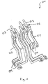
- Figure 1 shows an electrical functional component 01 with a plurality of conductor tracks 02, at the ends of which contact pins 03 are attached in an electrically conductive manner.
- the contact pins 03 are used to attach a Fig. 1 plug, not shown, on functional component 01.
- the conductor tracks 02 are produced by punching out a conductor plate, various connecting webs 04 initially remaining for reasons of assembly.
- the connecting webs 04 are removed after the functional component 01 is encapsulated with plastic, so that all conductor tracks 02 are electrically insulated from one another.
- An electrically conductive contact zone is present between the conductor tracks 02 and the contact pins 03, so that electrical current can be transmitted between the conductor tracks 02 and the contact pins 03 essentially without resistance.
- the electrical contact zone between the conductor tracks 02 and the contact pins 03 is realized by pressing the contact pins 03 into cylindrical recesses at the end of the conductor tracks 02, an annular, cold-pressure-welded transition zone being formed between the conductor tracks 02 and the contact pins 03 by the pressing of the contact pins 03 .
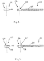
- FIG. 2 The conductor plate 05, from which the conductor tracks 02 are punched out, is first shown in cross section. At the end 06 of the conductor tracks 02, a recess 07 with a cylindrical cross section is made by means of a punching mandrel.
- Figure 3 represents the conductor track 02 after a further manufacturing step.
- the material of the conductor plate 05 is pulled through in the region of the recess 07 by means of a mandrel and the conductor plate 05 is cold-formed in the region of the recess 07 to form a protrusion 08.
- the conductor track 02 thus has a material thickening in the region of the recess 07, the thickness of which is greater than the thickness of the conductor plate 05 used.
- Figure 4 shows the conductor track 02 and the contact pin 03 immediately before being pressed into the recess 07.
- the contact pin 03 is produced by cutting wire sections to length, the cutting to length being carried out by tearing off the contact pins.
- a crack surface is therefore formed on each of the end faces 29, the crack surface in each case bordering on a material constriction 09 which is formed by tearing off the continuous wire.
- the outside diameter of the contact pin 03 is slightly larger, for example by a few tenths of a millimeter, than the inside diameter of the recess 07.
- the constriction 09 allows the contact pin 03 to be inserted and centered in the recess 07 without any problems before being pressed in.
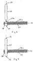
- Figure 5 shows the conductor track 02 and the contact pin 03 after pressing the contact pin 03 into the recess 07; it can be seen that the contact pin 03 projects with both ends beyond the end cross sections of the recess 07. In other words, this means that the contact pin 03 is pushed through the conductor track 02 in order to compensate for dimensional tolerances in the area of the material overlap between the inside diameter of the recess 07 and the outside diameter of the contact pin 03. Since the contact pin 03 is mirror-symmetrical with respect to its center and the two ends have the same shape, the contact pin 03 can be fed in and pressed in with both ends ahead.
- Figure 6 and Figure 7 schematically show a method for through-contacting two conductor tracks 02 and 02a by pressing in a contact pin 03.
- the two conductor tracks 02 and 02a are arranged one above the other in such a way that the two recesses 07 and 07a are aligned with one another.
- By pressing in the contact pin 03 the two ends 09 each projecting beyond the conductor tracks 02 and 02a, the conductor tracks are contacted with one another.
- An insulator layer 10 can be provided between the conductor tracks 02 and 02a.
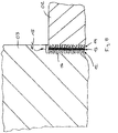
- Figure 8 shows the contact pin 03 and the conductor track 02 in enlarged section A according to Fig. 5 .
- an annular, cold-pressure-welded transition zone 11 is formed, which in Fig. 8 for easier understanding of the invention is only schematized and exemplified on an enlarged scale.
- an annular cold forming zone 12 which consists of the material of the contact pin 03
- an annular welding zone 13 in which the material of the contact pin 03 and the material of the conductor track 02 are integrally welded
- an annular cold forming zone 14 made of the material of the conductor track 02 arranged one behind the other.
- the cold forming zones 12 and 14 and the welding zone 13 arise when the contact pin 03 is pressed into the recess 07 of the conductor track 02 due to the material coverage between the outer circumference 15 of the contact pin 03 and the inner circumference 16 of the recess 07.
- the material coverage is dependent on the choice of material for the To select contact pin 03 and the conductor track 02 so that after pressing the contact pin 03 into the recess 07, a welding zone 13 is formed at least in some areas, in which the contact pin 03 is cold-welded to the conductor track 02. This can be easily checked by making micrographs.
- Fig. 8 illustrated geometry of the cold forming zones 12 and 14 and the welding zone 13 is only to be understood schematically, since the actual Ratios depend very much on the materials used.
- Figure 9 shows the end 06 of the conductor track 02 with the cylindrical recess 07 and the projection 08 in an enlarged cross section.
- Figure 10 shows the end 06 on the track 02 in a view from above. It can be seen that the material of the conductor track 02 encloses the recess 07 in a ring-shaped contact area 17.
- this ring-section-shaped contact area on the inner circumference 16 is not only plastically deformed, but also elastically expanded in the radial direction.
- This elastic expansion causes an elastic restoring force, by means of which the inner circumference 16 is pressed and prestressed against the outer circumference 15 after the contact pin 03 has been pressed in.
- This elastic prestressing of the ring-section-shaped contact region 17 allows creep and aging processes to be compensated for with regard to the electrical line quality, since the material of the conductor track 02 is pressed permanently against the material of the contact pin 03 by the elastic prestressing.
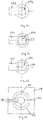
- Figure 11 shows an embodiment 02b of a conductor track.
- a recess 07b with a conical section which in turn also has a projection 08b reaches through.
- the opening angle of the conical recess 07b is in Fig. 11 exaggerated. In most cases, an opening angle of just a few degrees is sufficient to ensure the necessary tolerance compensation.
- Figure 12 shows the conductor track 02b in a view from above, the cross-sectional constriction of the recess 07b with the different diameters being recognized at the two end cross sections.
- Figure 13 shows a further example 02c of a conductor track, at the ends 06c of which a recess 07c is again made.
- the recess 07c also extends through the projection 08c.
- a conical chamfer 19 is attached to the upper end cross-section 18 of the recess 07c in order to facilitate the insertion and centering of the contact pin 03 before the pressing-in.
- Figure 14 shows the conductor track 02c with the chamfer 19 in a view from above.
- Figure 15 shows a further example 02d of a conductor track, on the cylindrical recesses 07d of which a radius 20 is attached in the area of the end cross section 18d, which in turn facilitates the insertion and centering of the contact pin 03 before the pressing.
- Figure 16 shows the conductor track 02d with the radius 20 in a view from above.
- Figure 17 shows a further example 02e of a conductor track with a cylindrical recess 07e, which has chamfers 19 at the end cross sections 21 and 22, respectively.
- the contact pin 03 can be pressed into the recess 07e either from below or from above.
- Figure 18 shows the conductor track 02e in a view from above.
- Figure 19 and Figure 20 show a further example 02f of a conductor track, the cylindrical recess 07f of which has radii 20 at the end cross sections 21 and 22, so that the contact pin 03 can be pressed into the conductor track either from above or from below.
- Figure 21 shows another example 02g of a conductor track with a prismatic recess 07g.
- the prismatic recess 07g has an essentially square cross section, the corners of which are rounded.
- the contact pin to be used in this case, which is pressed into the conductor track 02g, has a complementary shape in cross-section, again providing a suitable material covering in order to form the cold-press-welded transition zone when pressed in.
- Figure 22 and Figure 23 show examples 02h and 02i, which in turn have prismatic recesses 07h and 07i. Either a square chamfer 23 or a square radius 24 is attached to the end cross sections of the recesses 07h and 07i.
- Figure 24 shows a conductor track 25, the rectangular outer circumference of the conductor track 25 being understood only as an example.
- a recess 26 is provided in the conductor track 25, into which a contact pin 03 can be inserted.
- two relief slots 27 are additionally provided in the conductor track 25, which grip around the contact area 28 in sections.
- the relief slots 27 enable an elastic expansion of the annular contact area 28 in the area of the relief slots 27, so that the contact area 28 is elastically pre-tensioned after the contact pin 03 has been pressed in and elastically presses the inner circumference of the recess 26 against the outer circumference of the contact pin 03.
Landscapes
- Engineering & Computer Science (AREA)
- Manufacturing & Machinery (AREA)
- Mechanical Engineering (AREA)
- Microelectronics & Electronic Packaging (AREA)
- Manufacturing Of Electrical Connectors (AREA)
- Connections Effected By Soldering, Adhesion, Or Permanent Deformation (AREA)
- Coupling Device And Connection With Printed Circuit (AREA)
Claims (14)
- Composant (01) fonctionnel électrique comprenant au moins une piste (02b) conductrice et au moins une broche (03) de contact, la broche (03) de contact étant disposée à la piste (02b) conductrice et pouvant être contactée avec un élément de contact complémentaire en fonction, en particulier dans un connecteur mâle ou une douille, et une zone de contact étant prévue entre la piste (02b) conductrice et la broche (03) de contact, la zone de contact reliant la piste (02b) conductrice à la broche (03) de contact de manière électriquement conductrice, la zone de contact étant formée en pressant la broche (03) de contact dans un évidement (07b) de la piste (02b) conductrice, la zone de contact électriquement conductrice étant formée à la façon d'une zone (11) de transition annulaire et soudée par pression à froid, le matériau de surface de la piste (02b) conductrice et/ou le matériau de surface de la broche (03) de contact ayant au moins une zone (12, 14) de travail à froid dans la zone (11) de transition, et une zone (13) de soudage étant présente au moins par sections à ou dans au moins une zone (12, 14) de travail à froid, la broche (03) de contact et la piste (02b) conductrice étant reliées les unes aux autres de manière électriquement conductrice et par liaison de matière dans ladite zone (13) de soudage,
caractérisé en ce que
l'évidement (07b) recevant la broche (03) de contact a une coupe transversale en forme de tronçon conique, l'évidement se rétrécissant en direction de joint de la broche (03) de contact. - Composant fonctionnel électrique selon la revendication 1,
caractérisé en ce que
la piste (02b) conductrice est réalisée par une tôle (05) conductrice, en particulier par une grille de perforation. - Composant fonctionnel électrique selon la revendication 1 ou 2,
caractérisé en ce que
la piste (02b) conductrice comprend une saillie (08b) annulaire dans la région de la zone de contact, la saillie (08b) formant un renflement de matériau dans la piste (02b) conductrice. - Composant fonctionnel électrique selon l'une quelconque des revendications 1 à 3,
caractérisé en ce que
la broche (03) de contact s'engage totalement à travers la piste (02b) conductrice dans un évidement (07b) et fait saillie au moins en partie par-dessus la piste (02b) conductrice avec ses deux extrémités. - Composant fonctionnel électrique selon l'une quelconque des revendications 1 à 4,
caractérisé en ce que
la broche (03) de contact a un rétrécissement de la coupe transversale à au moins une extrémité, en particulier un chanfrein ou un rayon à au moins une coupe transversale d'extrémité ou une coupe transversale en forme de tronçon conique. - Composant fonctionnel électrique selon la revendication 5,
caractérisé en ce que
la broche (03) de contact a une surface de déchirure à au moins une face (29) frontale, la coupe transversale de la broche de contact étant rétrécie à la face (29) frontale. - Composant fonctionnel électrique selon l'une quelconque des revendications 1 à 6,
caractérisé en ce que
la broche (03) de contact a une circonférence (15) extérieure qui est calibrée au moins par sections et/ou que l'évidement (07b) a une circonférence (16) intérieure qui est calibrée au moins par sections. - Composant fonctionnel électrique selon l'une quelconque des revendications 1 à 7,
caractérisé en ce que
la piste (02b) conductrice et/ou la broche (03) de contact comprend/comprennent un revêtement métallique. - Composant fonctionnel électrique selon la revendication 8,
caractérisé en ce que
la résistance à la déformation du matériau de revêtement est moindre que la résistance à la déformation du matériau revêtu. - Composant fonctionnel électrique selon l'une quelconque des revendications 1 à 9,
caractérisé en ce que
le composant (01) fonctionnel est réalisé à la façon d'un circuit imprimé ou d'un connecteur mâle ou d'un agent lumineux. - Procédé pour la production d'un composant (01) fonctionnel électrique, comprenant les étapes de procédé suivantes :a) produire au moins un évidement (07b) ayant une coupe transversale en forme de tronçon conique dans une piste (02b) électriquement conductrice ;b) amener une broche (03) de contact dont la circonférence (15) extérieure est plus grande au moins par sections que la circonférence (16) intérieure de l'évidement (07b) en forme de tronçon conique, une extrémité de la broche (03) de contact étant disposée à ou insérée dans l'évidement (07b) en forme de tronçon conique, l'évidement (07b) se rétrécissant en direction de joint de la broche (03) de contact ;c) presser la broche (03) de contact dans l'évidement (07b) en forme de tronçon conique, une zone (11) de transition annulaire et soudée par pression à froid étant formée lors du pressage par le chevauchement des coupes transversales entre la broche (03) de contact d'une part et l'évidement (07b) dans la piste (02b) conductrice d'autre part, la broche (03) de contact et la piste (02b) conductrice étant reliées les unes aux autres de manière électriquement conductrice par liaison de matière dans la zone (13) de soudage de ladite zone (11) de transition.
- Procédé selon la revendication 11,
caractérisé en ce qu'
une tôle (05) conductrice est perforée dans l'étape de procédé a) en utilisant un outil de découpage. - Procédé selon la revendication 12,
caractérisé en ce que
la tôle (05) conductrice perforée est traversée, en particulier par un mandrin, résultant en une saillie (08b) annulaire. - Procédé selon l'une quelconque des revendications 11 à 13,
caractérisé en ce qu'
un matériau de fil continu est déchiré en sections de fil, en particulier ayant des rétrécissements à leurs extrémités, pour produire la broche (03) de contact, des surfaces de déchirure étant formées aux faces (29) frontales de la broche (03) de contact.
Applications Claiming Priority (2)
| Application Number | Priority Date | Filing Date | Title |
|---|---|---|---|
| DE102015100149.7A DE102015100149A1 (de) | 2015-01-08 | 2015-01-08 | Elektrisches Funktionsbauteil mit Kontaktstift und Verfahren zur Herstellung eines elektrischen Funktionsbauteils |
| PCT/EP2015/079246 WO2016110369A1 (fr) | 2015-01-08 | 2015-12-10 | Composant fonctionnel électrique à broche de contact et procédé de fabrication d'un composant fonctionnel électrique |
Publications (2)
| Publication Number | Publication Date |
|---|---|
| EP3243246A1 EP3243246A1 (fr) | 2017-11-15 |
| EP3243246B1 true EP3243246B1 (fr) | 2020-04-29 |
Family
ID=55027699
Family Applications (1)
| Application Number | Title | Priority Date | Filing Date |
|---|---|---|---|
| EP15817113.2A Active EP3243246B1 (fr) | 2015-01-08 | 2015-12-10 | Composant fonctionnel électrique à broche de contact et procédé de fabrication d'un composant fonctionnel électrique |
Country Status (5)
| Country | Link |
|---|---|
| US (1) | US10700445B2 (fr) |
| EP (1) | EP3243246B1 (fr) |
| CN (1) | CN107112706B (fr) |
| DE (1) | DE102015100149A1 (fr) |
| WO (1) | WO2016110369A1 (fr) |
Families Citing this family (6)
| Publication number | Priority date | Publication date | Assignee | Title |
|---|---|---|---|---|
| DE102015119785B4 (de) * | 2015-11-04 | 2020-03-26 | ept Holding GmbH & Co. KG | Lochkontur für Einpresstechnik in ein Stanzgitter |
| DE102017109034B4 (de) | 2017-04-27 | 2021-11-11 | Te Connectivity Germany Gmbh | Steckverbindung, elektrischer Stecker und Verfahren zur Herstellung einer elektrischen Verbindung |
| DE102017110696B4 (de) | 2017-05-17 | 2025-01-30 | Hanon Systems | Motorgehäuse eines Verdichters und Verfahren zur Kontaktierung eines elektrischen Motors |
| DE102018218001B4 (de) * | 2018-10-22 | 2021-09-30 | Schott Ag | Verfahren zur Herstellung eines Anschlussstiftes für Durchführungen, sowie Anschlussstift |
| DE102019203166A1 (de) * | 2019-03-08 | 2020-09-10 | Zf Friedrichshafen Ag | Verbindung einer Stromschiene mit einem weiteren stromführenden Element |
| WO2022271665A1 (fr) | 2021-06-21 | 2022-12-29 | Milwaukee Electric Tool Corporation | Connecteur électrique à broche de poussée |
Citations (1)
| Publication number | Priority date | Publication date | Assignee | Title |
|---|---|---|---|---|
| US3718750A (en) | 1971-10-12 | 1973-02-27 | Gen Motors Corp | Electrical connector |
Family Cites Families (18)
| Publication number | Priority date | Publication date | Assignee | Title |
|---|---|---|---|---|
| US3252204A (en) * | 1962-12-19 | 1966-05-24 | Gen Motors Corp | Method of mounting a connector member to a support member |
| US3805214A (en) * | 1972-08-22 | 1974-04-16 | Amp Inc | Resilient electrical contact |
| US5083928A (en) | 1991-04-25 | 1992-01-28 | E. I. Du Pont De Nemours And Company | Electrical pin tips |
| SE510056C2 (sv) * | 1997-08-07 | 1999-04-12 | Ssab Hardtech Ab | Sätt att tillverka en härdad ståldetalj |
| GB2330336A (en) * | 1997-10-14 | 1999-04-21 | Alliedsignal Ltd | Energy absorbing device for a seat belt |
| DE10138458A1 (de) * | 2001-08-04 | 2003-02-27 | Siemens Ag | Elektrische Schaltung mit streifenförmigen Leitern |
| EP1720387A1 (fr) * | 2005-05-03 | 2006-11-08 | Franz Broch | Contact à haut courant avec une portion de serrage |
| US8092129B2 (en) * | 2006-04-21 | 2012-01-10 | Hubbell Incorporated | Bonding washer |
| WO2010093971A1 (fr) * | 2009-02-13 | 2010-08-19 | Once Innovations, Inc. | Ensemble diode électroluminescente et procédés |
| DE202009017984U1 (de) * | 2009-09-26 | 2010-09-30 | Amphenol-Tuchel Electronics Gmbh | Einpressverbinder |
| DE102010001418A1 (de) | 2010-02-01 | 2011-08-04 | Robert Bosch GmbH, 70469 | Sensormodul, Verfahren zur Herstellung eines Sensormoduls |
| JP5570383B2 (ja) * | 2010-10-15 | 2014-08-13 | 株式会社神戸製鋼所 | 導電性連結部材、導電性連結部材の製造方法、及び導電性連結部材が電極とされたバッテリ |
| DE112012003618T5 (de) * | 2011-08-29 | 2014-05-22 | Lithium Energy Japan | Verbindungskörper, Herstellungsverfahren des Verbindungskörpers, elektrische Speichervorrichtung und Herstellungsverfahren der elektrischen Speichervorrichtung |
| EP2658036B1 (fr) * | 2011-10-06 | 2019-06-12 | Tyco Electronics Belgium EC BVBA | Ensemble formant connexion électrique |
| DE102011122371A1 (de) * | 2011-12-22 | 2013-06-27 | Kathrein-Werke Kg | Elektrische Anschlusseinrichtung zur Herstellung einer Lötverbindung |
| US9021682B2 (en) * | 2011-12-29 | 2015-05-05 | Taiwan Semiconductor Manufacturing Company, Ltd. | Apparatus for stud bump formation |
| DE102013111963A1 (de) | 2012-11-14 | 2014-05-15 | Walter Söhner GmbH & Co. KG | Plattenelement mit Tiefziehbohrung für Einpresskontakte |
| DE102014208101A1 (de) | 2014-04-29 | 2015-10-29 | Robert Bosch Gmbh | Elektrische Verbindungsanordnung für die elektrische Verbindung von Leiterplatten untereinander mittels lötfreier Einpresskontaktierung |
-
2015
- 2015-01-08 DE DE102015100149.7A patent/DE102015100149A1/de not_active Withdrawn
- 2015-12-10 US US15/541,198 patent/US10700445B2/en active Active
- 2015-12-10 CN CN201580072348.4A patent/CN107112706B/zh active Active
- 2015-12-10 WO PCT/EP2015/079246 patent/WO2016110369A1/fr not_active Ceased
- 2015-12-10 EP EP15817113.2A patent/EP3243246B1/fr active Active
Patent Citations (1)
| Publication number | Priority date | Publication date | Assignee | Title |
|---|---|---|---|---|
| US3718750A (en) | 1971-10-12 | 1973-02-27 | Gen Motors Corp | Electrical connector |
Non-Patent Citations (8)
| Title |
|---|
| ANONYMOUS: "CuNi9Sn2 Werkstoff-Datenblätter", DEUTSCHES KUPFERINSTITUT, 2005, pages 1 - 11, XP055779261 |
| ANONYMOUS: "CuZn30 Werkstoff-Datenblätter", DEUTSCHES KUPFERINSTITUT, 2005, pages 1 - 12, XP055779265 |
| ANONYMOUS: "Diaphragm / piston pressure switches hex 27 with integrated connector", SUCO PROSPECT 0132 - 0137, pages 1 - 2 |
| ANONYMOUS: "Membran- / Kolbendruckschalter SW 27 mit integriertem Stecker", SUCO PROSPECT 0132 - 0137, pages 1 - 2 |
| ANONYMOUS: "Präzisionskontaktstifte für elektrische Steckverbinder", ELBIK GMBH, PRESSEMITTEILUNG - PRESSEBOX, 23 April 2006 (2006-04-23), pages 1 - 2, XP055779269, Retrieved from the Internet <URL:https://www.pressebox.de/inaktiv/elbik-gmbh/Praezisionskontaktstifte-fuer-elektrische-Steckverbinder/boxid/84445> |
| HUBER: "Einpresstechnik", DATENBLATT, 1 February 2017 (2017-02-01), pages 1 - 17, XP093184484 |
| ROLAND H. KILGUS: "Metalltechnik Der Werkzeugbau9. neubearbeitete Auflage", 1986, VERLAG EUROPA-LEHRMITTEL, article "1.2 Scherschneiden", pages: 3, 8 - 9, XP055779252 |
| WOLFGANG BRANDT: "Kontaktstifte / thermisch gerissene Kontaktstifte für Stecker, Steckverbinder, Pfostenleisten usw.", 29 November 2013 (2013-11-29), pages 1 - 3, XP055779277, Retrieved from the Internet <URL:http://www.antriebstechnik.eu/kontaktstifte.htm> |
Also Published As
| Publication number | Publication date |
|---|---|
| US10700445B2 (en) | 2020-06-30 |
| EP3243246A1 (fr) | 2017-11-15 |
| WO2016110369A1 (fr) | 2016-07-14 |
| CN107112706A (zh) | 2017-08-29 |
| US20170365936A1 (en) | 2017-12-21 |
| CN107112706B (zh) | 2020-07-10 |
| DE102015100149A1 (de) | 2016-07-14 |
Similar Documents
| Publication | Publication Date | Title |
|---|---|---|
| EP3243246B1 (fr) | Composant fonctionnel électrique à broche de contact et procédé de fabrication d'un composant fonctionnel électrique | |
| EP3031564B1 (fr) | Element auxiliaire pour etre presse dans une premiere piece dans un procede de soudage de pieces non soudables directement | |
| EP2130418B1 (fr) | Procédé d'introduction d'une broche dans une ouverture de réception d'une carte de circuits imprimés | |
| EP1997187A1 (fr) | Broche de contact et son procédé de fabrication | |
| DE102018119844A1 (de) | Elektrische Verbindung sowie Verfahren zur Herstellung einer elektrischen Verbindung | |
| DE102013209407B4 (de) | Verfahren zur lötfreien elektrischen Einpresskontaktierung von elektrisch leitfähigen Einpress-Stiften in Leiterplatten | |
| EP2796017B1 (fr) | Procédé de réalisation d'une liaison électrique haute-fréquence entre deux segments conducteurs en forme de plaques ainsi qu'une liaison électrique haute-fréquence associée | |
| DE102014208101A1 (de) | Elektrische Verbindungsanordnung für die elektrische Verbindung von Leiterplatten untereinander mittels lötfreier Einpresskontaktierung | |
| EP3022805A1 (fr) | Dispositif de contact pour la réalisation d'une connexion électrique avec le site de contact d'un circuit imprimé | |
| EP2920847B1 (fr) | Élément carte pourvu d'un alésage embouti pour contacts à encastrer | |
| EP3157769B1 (fr) | Procédé servant à fabriquer un composant de châssis | |
| EP2638988B1 (fr) | Système comprenant un rivet auto-poinçonneur et des pièces à assembler, et procédé d'assemblage desdites pièces avec ledit rivet | |
| DE102010039204A1 (de) | Elektrische Kontaktierung | |
| WO2006005291A1 (fr) | Procede de liaison d'au moins un conducteur a un element de contact | |
| EP1003243A2 (fr) | Procédé de fabrication d'une connexion électrique à une partie en tôle et ensemble de montage | |
| EP1898496B1 (fr) | Elément de contact métallique pour un agencement de contact électrique | |
| DE102021113511B3 (de) | Widerstandsschweißverfahren und Vorrichtung zum Widerstandsschweißen | |
| EP3629420B1 (fr) | Connection insérée à la force | |
| DE102015119785A1 (de) | Lochkontur für Einpresstechnik in ein Stanzgitter | |
| EP3800749B1 (fr) | Procédé de fabrication d'un élément de contact électroconducteur, élément de contact électroconducteur et manchon doté d'un élément de contact électroconducteur | |
| DE102012222254A1 (de) | Bauteilverbund zweier der Stromleitung dienender Bauteile, Verfahren zur Herstellung eines Bauteilverbunds und Verwendung eines Bauteilverbunds | |
| EP3736920B1 (fr) | Borne de contact et son procédé de fabrication | |
| EP4738615A1 (fr) | Dispositif de connexion et procédé de fabrication d'un dispositif de connexion | |
| EP4113128A1 (fr) | Procédé de fabrication d'un dispositif de mesure des niveaux de courant et dispositif de mesure des niveaux de courant | |
| DE102023136189A1 (de) | Verbindungselement, Anordnung und Verfahren |
Legal Events
| Date | Code | Title | Description |
|---|---|---|---|
| STAA | Information on the status of an ep patent application or granted ep patent |
Free format text: STATUS: THE INTERNATIONAL PUBLICATION HAS BEEN MADE |
|
| PUAI | Public reference made under article 153(3) epc to a published international application that has entered the european phase |
Free format text: ORIGINAL CODE: 0009012 |
|
| STAA | Information on the status of an ep patent application or granted ep patent |
Free format text: STATUS: REQUEST FOR EXAMINATION WAS MADE |
|
| 17P | Request for examination filed |
Effective date: 20170707 |
|
| AK | Designated contracting states |
Kind code of ref document: A1 Designated state(s): AL AT BE BG CH CY CZ DE DK EE ES FI FR GB GR HR HU IE IS IT LI LT LU LV MC MK MT NL NO PL PT RO RS SE SI SK SM TR |
|
| AX | Request for extension of the european patent |
Extension state: BA ME |
|
| DAV | Request for validation of the european patent (deleted) | ||
| DAX | Request for extension of the european patent (deleted) | ||
| STAA | Information on the status of an ep patent application or granted ep patent |
Free format text: STATUS: EXAMINATION IS IN PROGRESS |
|
| 17Q | First examination report despatched |
Effective date: 20190614 |
|
| GRAP | Despatch of communication of intention to grant a patent |
Free format text: ORIGINAL CODE: EPIDOSNIGR1 |
|
| STAA | Information on the status of an ep patent application or granted ep patent |
Free format text: STATUS: GRANT OF PATENT IS INTENDED |
|
| INTG | Intention to grant announced |
Effective date: 20191219 |
|
| GRAS | Grant fee paid |
Free format text: ORIGINAL CODE: EPIDOSNIGR3 |
|
| GRAA | (expected) grant |
Free format text: ORIGINAL CODE: 0009210 |
|
| STAA | Information on the status of an ep patent application or granted ep patent |
Free format text: STATUS: THE PATENT HAS BEEN GRANTED |
|
| AK | Designated contracting states |
Kind code of ref document: B1 Designated state(s): AL AT BE BG CH CY CZ DE DK EE ES FI FR GB GR HR HU IE IS IT LI LT LU LV MC MK MT NL NO PL PT RO RS SE SI SK SM TR |
|
| REG | Reference to a national code |
Ref country code: GB Ref legal event code: FG4D Free format text: NOT ENGLISH |
|
| REG | Reference to a national code |
Ref country code: CH Ref legal event code: EP |
|
| REG | Reference to a national code |
Ref country code: AT Ref legal event code: REF Ref document number: 1264710 Country of ref document: AT Kind code of ref document: T Effective date: 20200515 |
|
| REG | Reference to a national code |
Ref country code: DE Ref legal event code: R096 Ref document number: 502015012463 Country of ref document: DE |
|
| REG | Reference to a national code |
Ref country code: IE Ref legal event code: FG4D Free format text: LANGUAGE OF EP DOCUMENT: GERMAN |
|
| REG | Reference to a national code |
Ref country code: NL Ref legal event code: MP Effective date: 20200429 |
|
| REG | Reference to a national code |
Ref country code: LT Ref legal event code: MG4D |
|
| PG25 | Lapsed in a contracting state [announced via postgrant information from national office to epo] |
Ref country code: GR Free format text: LAPSE BECAUSE OF FAILURE TO SUBMIT A TRANSLATION OF THE DESCRIPTION OR TO PAY THE FEE WITHIN THE PRESCRIBED TIME-LIMIT Effective date: 20200730 Ref country code: LT Free format text: LAPSE BECAUSE OF FAILURE TO SUBMIT A TRANSLATION OF THE DESCRIPTION OR TO PAY THE FEE WITHIN THE PRESCRIBED TIME-LIMIT Effective date: 20200429 Ref country code: SE Free format text: LAPSE BECAUSE OF FAILURE TO SUBMIT A TRANSLATION OF THE DESCRIPTION OR TO PAY THE FEE WITHIN THE PRESCRIBED TIME-LIMIT Effective date: 20200429 Ref country code: NO Free format text: LAPSE BECAUSE OF FAILURE TO SUBMIT A TRANSLATION OF THE DESCRIPTION OR TO PAY THE FEE WITHIN THE PRESCRIBED TIME-LIMIT Effective date: 20200729 Ref country code: PT Free format text: LAPSE BECAUSE OF FAILURE TO SUBMIT A TRANSLATION OF THE DESCRIPTION OR TO PAY THE FEE WITHIN THE PRESCRIBED TIME-LIMIT Effective date: 20200831 Ref country code: FI Free format text: LAPSE BECAUSE OF FAILURE TO SUBMIT A TRANSLATION OF THE DESCRIPTION OR TO PAY THE FEE WITHIN THE PRESCRIBED TIME-LIMIT Effective date: 20200429 Ref country code: IS Free format text: LAPSE BECAUSE OF FAILURE TO SUBMIT A TRANSLATION OF THE DESCRIPTION OR TO PAY THE FEE WITHIN THE PRESCRIBED TIME-LIMIT Effective date: 20200829 |
|
| PG25 | Lapsed in a contracting state [announced via postgrant information from national office to epo] |
Ref country code: RS Free format text: LAPSE BECAUSE OF FAILURE TO SUBMIT A TRANSLATION OF THE DESCRIPTION OR TO PAY THE FEE WITHIN THE PRESCRIBED TIME-LIMIT Effective date: 20200429 Ref country code: LV Free format text: LAPSE BECAUSE OF FAILURE TO SUBMIT A TRANSLATION OF THE DESCRIPTION OR TO PAY THE FEE WITHIN THE PRESCRIBED TIME-LIMIT Effective date: 20200429 Ref country code: HR Free format text: LAPSE BECAUSE OF FAILURE TO SUBMIT A TRANSLATION OF THE DESCRIPTION OR TO PAY THE FEE WITHIN THE PRESCRIBED TIME-LIMIT Effective date: 20200429 Ref country code: BG Free format text: LAPSE BECAUSE OF FAILURE TO SUBMIT A TRANSLATION OF THE DESCRIPTION OR TO PAY THE FEE WITHIN THE PRESCRIBED TIME-LIMIT Effective date: 20200729 |
|
| PG25 | Lapsed in a contracting state [announced via postgrant information from national office to epo] |
Ref country code: AL Free format text: LAPSE BECAUSE OF FAILURE TO SUBMIT A TRANSLATION OF THE DESCRIPTION OR TO PAY THE FEE WITHIN THE PRESCRIBED TIME-LIMIT Effective date: 20200429 Ref country code: NL Free format text: LAPSE BECAUSE OF FAILURE TO SUBMIT A TRANSLATION OF THE DESCRIPTION OR TO PAY THE FEE WITHIN THE PRESCRIBED TIME-LIMIT Effective date: 20200429 |
|
| PG25 | Lapsed in a contracting state [announced via postgrant information from national office to epo] |
Ref country code: EE Free format text: LAPSE BECAUSE OF FAILURE TO SUBMIT A TRANSLATION OF THE DESCRIPTION OR TO PAY THE FEE WITHIN THE PRESCRIBED TIME-LIMIT Effective date: 20200429 Ref country code: SM Free format text: LAPSE BECAUSE OF FAILURE TO SUBMIT A TRANSLATION OF THE DESCRIPTION OR TO PAY THE FEE WITHIN THE PRESCRIBED TIME-LIMIT Effective date: 20200429 Ref country code: CZ Free format text: LAPSE BECAUSE OF FAILURE TO SUBMIT A TRANSLATION OF THE DESCRIPTION OR TO PAY THE FEE WITHIN THE PRESCRIBED TIME-LIMIT Effective date: 20200429 Ref country code: RO Free format text: LAPSE BECAUSE OF FAILURE TO SUBMIT A TRANSLATION OF THE DESCRIPTION OR TO PAY THE FEE WITHIN THE PRESCRIBED TIME-LIMIT Effective date: 20200429 Ref country code: IT Free format text: LAPSE BECAUSE OF FAILURE TO SUBMIT A TRANSLATION OF THE DESCRIPTION OR TO PAY THE FEE WITHIN THE PRESCRIBED TIME-LIMIT Effective date: 20200429 Ref country code: DK Free format text: LAPSE BECAUSE OF FAILURE TO SUBMIT A TRANSLATION OF THE DESCRIPTION OR TO PAY THE FEE WITHIN THE PRESCRIBED TIME-LIMIT Effective date: 20200429 Ref country code: ES Free format text: LAPSE BECAUSE OF FAILURE TO SUBMIT A TRANSLATION OF THE DESCRIPTION OR TO PAY THE FEE WITHIN THE PRESCRIBED TIME-LIMIT Effective date: 20200429 |
|
| REG | Reference to a national code |
Ref country code: DE Ref legal event code: R026 Ref document number: 502015012463 Country of ref document: DE |
|
| PLBI | Opposition filed |
Free format text: ORIGINAL CODE: 0009260 |
|
| PLAX | Notice of opposition and request to file observation + time limit sent |
Free format text: ORIGINAL CODE: EPIDOSNOBS2 |
|
| PG25 | Lapsed in a contracting state [announced via postgrant information from national office to epo] |
Ref country code: SK Free format text: LAPSE BECAUSE OF FAILURE TO SUBMIT A TRANSLATION OF THE DESCRIPTION OR TO PAY THE FEE WITHIN THE PRESCRIBED TIME-LIMIT Effective date: 20200429 Ref country code: PL Free format text: LAPSE BECAUSE OF FAILURE TO SUBMIT A TRANSLATION OF THE DESCRIPTION OR TO PAY THE FEE WITHIN THE PRESCRIBED TIME-LIMIT Effective date: 20200429 |
|
| 26 | Opposition filed |
Opponent name: EGON NESPER GMBH & CO. KG. Effective date: 20210129 |
|
| PG25 | Lapsed in a contracting state [announced via postgrant information from national office to epo] |
Ref country code: SI Free format text: LAPSE BECAUSE OF FAILURE TO SUBMIT A TRANSLATION OF THE DESCRIPTION OR TO PAY THE FEE WITHIN THE PRESCRIBED TIME-LIMIT Effective date: 20200429 |
|
| PLBB | Reply of patent proprietor to notice(s) of opposition received |
Free format text: ORIGINAL CODE: EPIDOSNOBS3 |
|
| REG | Reference to a national code |
Ref country code: CH Ref legal event code: PL |
|
| PG25 | Lapsed in a contracting state [announced via postgrant information from national office to epo] |
Ref country code: MC Free format text: LAPSE BECAUSE OF FAILURE TO SUBMIT A TRANSLATION OF THE DESCRIPTION OR TO PAY THE FEE WITHIN THE PRESCRIBED TIME-LIMIT Effective date: 20200429 |
|
| REG | Reference to a national code |
Ref country code: BE Ref legal event code: MM Effective date: 20201231 |
|
| PLAY | Examination report in opposition despatched + time limit |
Free format text: ORIGINAL CODE: EPIDOSNORE2 |
|
| PG25 | Lapsed in a contracting state [announced via postgrant information from national office to epo] |
Ref country code: LU Free format text: LAPSE BECAUSE OF NON-PAYMENT OF DUE FEES Effective date: 20201210 Ref country code: IE Free format text: LAPSE BECAUSE OF NON-PAYMENT OF DUE FEES Effective date: 20201210 |
|
| PLBC | Reply to examination report in opposition received |
Free format text: ORIGINAL CODE: EPIDOSNORE3 |
|
| PG25 | Lapsed in a contracting state [announced via postgrant information from national office to epo] |
Ref country code: LI Free format text: LAPSE BECAUSE OF NON-PAYMENT OF DUE FEES Effective date: 20201231 Ref country code: CH Free format text: LAPSE BECAUSE OF NON-PAYMENT OF DUE FEES Effective date: 20201231 |
|
| PG25 | Lapsed in a contracting state [announced via postgrant information from national office to epo] |
Ref country code: TR Free format text: LAPSE BECAUSE OF FAILURE TO SUBMIT A TRANSLATION OF THE DESCRIPTION OR TO PAY THE FEE WITHIN THE PRESCRIBED TIME-LIMIT Effective date: 20200429 Ref country code: MT Free format text: LAPSE BECAUSE OF FAILURE TO SUBMIT A TRANSLATION OF THE DESCRIPTION OR TO PAY THE FEE WITHIN THE PRESCRIBED TIME-LIMIT Effective date: 20200429 Ref country code: CY Free format text: LAPSE BECAUSE OF FAILURE TO SUBMIT A TRANSLATION OF THE DESCRIPTION OR TO PAY THE FEE WITHIN THE PRESCRIBED TIME-LIMIT Effective date: 20200429 |
|
| PG25 | Lapsed in a contracting state [announced via postgrant information from national office to epo] |
Ref country code: MK Free format text: LAPSE BECAUSE OF FAILURE TO SUBMIT A TRANSLATION OF THE DESCRIPTION OR TO PAY THE FEE WITHIN THE PRESCRIBED TIME-LIMIT Effective date: 20200429 |
|
| PG25 | Lapsed in a contracting state [announced via postgrant information from national office to epo] |
Ref country code: BE Free format text: LAPSE BECAUSE OF NON-PAYMENT OF DUE FEES Effective date: 20201231 |
|
| PLAY | Examination report in opposition despatched + time limit |
Free format text: ORIGINAL CODE: EPIDOSNORE2 |
|
| PLBC | Reply to examination report in opposition received |
Free format text: ORIGINAL CODE: EPIDOSNORE3 |
|
| PLAP | Information related to despatch of examination report in opposition + time limit deleted |
Free format text: ORIGINAL CODE: EPIDOSDORE2 |
|
| PLAT | Information related to reply to examination report in opposition deleted |
Free format text: ORIGINAL CODE: EPIDOSDORE3 |
|
| PLAB | Opposition data, opponent's data or that of the opponent's representative modified |
Free format text: ORIGINAL CODE: 0009299OPPO |
|
| R26 | Opposition filed (corrected) |
Opponent name: EGON NESPER GMBH & CO. KG. Effective date: 20210129 |
|
| PLCK | Communication despatched that opposition was rejected |
Free format text: ORIGINAL CODE: EPIDOSNREJ1 |
|
| APBP | Date of receipt of notice of appeal recorded |
Free format text: ORIGINAL CODE: EPIDOSNNOA2O |
|
| APAH | Appeal reference modified |
Free format text: ORIGINAL CODE: EPIDOSCREFNO |
|
| APBQ | Date of receipt of statement of grounds of appeal recorded |
Free format text: ORIGINAL CODE: EPIDOSNNOA3O |
|
| PGFP | Annual fee paid to national office [announced via postgrant information from national office to epo] |
Ref country code: GB Payment date: 20251218 Year of fee payment: 11 |
|
| PGFP | Annual fee paid to national office [announced via postgrant information from national office to epo] |
Ref country code: AT Payment date: 20251215 Year of fee payment: 11 |
|
| PGFP | Annual fee paid to national office [announced via postgrant information from national office to epo] |
Ref country code: FR Payment date: 20251218 Year of fee payment: 11 |
|
| PGFP | Annual fee paid to national office [announced via postgrant information from national office to epo] |
Ref country code: DE Payment date: 20260218 Year of fee payment: 11 |