EP2929535B1 - Varisator - Google Patents
Varisator Download PDFInfo
- Publication number
- EP2929535B1 EP2929535B1 EP13801586.2A EP13801586A EP2929535B1 EP 2929535 B1 EP2929535 B1 EP 2929535B1 EP 13801586 A EP13801586 A EP 13801586A EP 2929535 B1 EP2929535 B1 EP 2929535B1
- Authority
- EP
- European Patent Office
- Prior art keywords
- layer
- voltage
- state
- ferroelectric
- superconductive
- Prior art date
- Legal status (The legal status is an assumption and is not a legal conclusion. Google has not performed a legal analysis and makes no representation as to the accuracy of the status listed.)
- Active
Links
- 239000000463 material Substances 0.000 claims description 158
- 239000004020 conductor Substances 0.000 claims description 18
- 230000005684 electric field Effects 0.000 claims description 18
- 239000012777 electrically insulating material Substances 0.000 claims description 6
- 230000003446 memory effect Effects 0.000 claims description 4
- 239000002887 superconductor Substances 0.000 claims description 3
- 229910002902 BiFeO3 Inorganic materials 0.000 claims description 2
- 229910052761 rare earth metal Inorganic materials 0.000 claims description 2
- 150000002910 rare earth metals Chemical class 0.000 claims description 2
- 229910003098 YBa2Cu3O7−x Inorganic materials 0.000 claims 1
- 229910002113 barium titanate Inorganic materials 0.000 claims 1
- 230000010287 polarization Effects 0.000 description 42
- 229910021521 yttrium barium copper oxide Inorganic materials 0.000 description 22
- 230000006870 function Effects 0.000 description 9
- 239000011810 insulating material Substances 0.000 description 7
- PCHJSUWPFVWCPO-UHFFFAOYSA-N gold Chemical compound [Au] PCHJSUWPFVWCPO-UHFFFAOYSA-N 0.000 description 5
- 239000010931 gold Substances 0.000 description 5
- 229910052737 gold Inorganic materials 0.000 description 5
- 235000012431 wafers Nutrition 0.000 description 5
- 239000002800 charge carrier Substances 0.000 description 4
- 238000005259 measurement Methods 0.000 description 4
- 238000001816 cooling Methods 0.000 description 2
- 241000954177 Bangana ariza Species 0.000 description 1
- 238000009825 accumulation Methods 0.000 description 1
- 230000000903 blocking effect Effects 0.000 description 1
- 230000007547 defect Effects 0.000 description 1
- 230000006735 deficit Effects 0.000 description 1
- 238000005265 energy consumption Methods 0.000 description 1
- 238000002474 experimental method Methods 0.000 description 1
- 230000004907 flux Effects 0.000 description 1
- 239000003607 modifier Substances 0.000 description 1
- 230000002441 reversible effect Effects 0.000 description 1
Images



Classifications
-
- H—ELECTRICITY
- H01—ELECTRIC ELEMENTS
- H01C—RESISTORS
- H01C7/00—Non-adjustable resistors formed as one or more layers or coatings; Non-adjustable resistors made from powdered conducting material or powdered semi-conducting material with or without insulating material
- H01C7/10—Non-adjustable resistors formed as one or more layers or coatings; Non-adjustable resistors made from powdered conducting material or powdered semi-conducting material with or without insulating material voltage responsive, i.e. varistors
-
- G—PHYSICS
- G11—INFORMATION STORAGE
- G11C—STATIC STORES
- G11C11/00—Digital stores characterised by the use of particular electric or magnetic storage elements; Storage elements therefor
- G11C11/21—Digital stores characterised by the use of particular electric or magnetic storage elements; Storage elements therefor using electric elements
- G11C11/22—Digital stores characterised by the use of particular electric or magnetic storage elements; Storage elements therefor using electric elements using ferroelectric elements
-
- G—PHYSICS
- G11—INFORMATION STORAGE
- G11C—STATIC STORES
- G11C11/00—Digital stores characterised by the use of particular electric or magnetic storage elements; Storage elements therefor
- G11C11/21—Digital stores characterised by the use of particular electric or magnetic storage elements; Storage elements therefor using electric elements
- G11C11/44—Digital stores characterised by the use of particular electric or magnetic storage elements; Storage elements therefor using electric elements using super-conductive elements, e.g. cryotron
-
- G—PHYSICS
- G11—INFORMATION STORAGE
- G11C—STATIC STORES
- G11C11/00—Digital stores characterised by the use of particular electric or magnetic storage elements; Storage elements therefor
- G11C11/54—Digital stores characterised by the use of particular electric or magnetic storage elements; Storage elements therefor using elements simulating biological cells, e.g. neuron
-
- G—PHYSICS
- G11—INFORMATION STORAGE
- G11C—STATIC STORES
- G11C11/00—Digital stores characterised by the use of particular electric or magnetic storage elements; Storage elements therefor
- G11C11/56—Digital stores characterised by the use of particular electric or magnetic storage elements; Storage elements therefor using storage elements with more than two stable states represented by steps, e.g. of voltage, current, phase, frequency
- G11C11/5657—Digital stores characterised by the use of particular electric or magnetic storage elements; Storage elements therefor using storage elements with more than two stable states represented by steps, e.g. of voltage, current, phase, frequency using ferroelectric storage elements
-
- G—PHYSICS
- G11—INFORMATION STORAGE
- G11C—STATIC STORES
- G11C13/00—Digital stores characterised by the use of storage elements not covered by groups G11C11/00, G11C23/00, or G11C25/00
- G11C13/0002—Digital stores characterised by the use of storage elements not covered by groups G11C11/00, G11C23/00, or G11C25/00 using resistive RAM [RRAM] elements
-
- H—ELECTRICITY
- H10—SEMICONDUCTOR DEVICES; ELECTRIC SOLID-STATE DEVICES NOT OTHERWISE PROVIDED FOR
- H10N—ELECTRIC SOLID-STATE DEVICES NOT OTHERWISE PROVIDED FOR
- H10N60/00—Superconducting devices
- H10N60/10—Junction-based devices
-
- H—ELECTRICITY
- H10—SEMICONDUCTOR DEVICES; ELECTRIC SOLID-STATE DEVICES NOT OTHERWISE PROVIDED FOR
- H10N—ELECTRIC SOLID-STATE DEVICES NOT OTHERWISE PROVIDED FOR
- H10N60/00—Superconducting devices
- H10N60/80—Constructional details
- H10N60/85—Superconducting active materials
- H10N60/855—Ceramic superconductors
- H10N60/857—Ceramic superconductors comprising copper oxide
-
- H—ELECTRICITY
- H10—SEMICONDUCTOR DEVICES; ELECTRIC SOLID-STATE DEVICES NOT OTHERWISE PROVIDED FOR
- H10N—ELECTRIC SOLID-STATE DEVICES NOT OTHERWISE PROVIDED FOR
- H10N70/00—Solid-state devices having no potential barriers, and specially adapted for rectifying, amplifying, oscillating or switching
- H10N70/20—Multistable switching devices, e.g. memristors
-
- H—ELECTRICITY
- H10—SEMICONDUCTOR DEVICES; ELECTRIC SOLID-STATE DEVICES NOT OTHERWISE PROVIDED FOR
- H10N—ELECTRIC SOLID-STATE DEVICES NOT OTHERWISE PROVIDED FOR
- H10N70/00—Solid-state devices having no potential barriers, and specially adapted for rectifying, amplifying, oscillating or switching
- H10N70/801—Constructional details of multistable switching devices
- H10N70/821—Device geometry
- H10N70/826—Device geometry adapted for essentially vertical current flow, e.g. sandwich or pillar type devices
-
- H—ELECTRICITY
- H10—SEMICONDUCTOR DEVICES; ELECTRIC SOLID-STATE DEVICES NOT OTHERWISE PROVIDED FOR
- H10N—ELECTRIC SOLID-STATE DEVICES NOT OTHERWISE PROVIDED FOR
- H10N70/00—Solid-state devices having no potential barriers, and specially adapted for rectifying, amplifying, oscillating or switching
- H10N70/801—Constructional details of multistable switching devices
- H10N70/841—Electrodes
-
- H—ELECTRICITY
- H10—SEMICONDUCTOR DEVICES; ELECTRIC SOLID-STATE DEVICES NOT OTHERWISE PROVIDED FOR
- H10N—ELECTRIC SOLID-STATE DEVICES NOT OTHERWISE PROVIDED FOR
- H10N70/00—Solid-state devices having no potential barriers, and specially adapted for rectifying, amplifying, oscillating or switching
- H10N70/801—Constructional details of multistable switching devices
- H10N70/881—Switching materials
- H10N70/883—Oxides or nitrides
- H10N70/8836—Complex metal oxides, e.g. perovskites, spinels
-
- G—PHYSICS
- G11—INFORMATION STORAGE
- G11C—STATIC STORES
- G11C2213/00—Indexing scheme relating to G11C13/00 for features not covered by this group
- G11C2213/50—Resistive cell structure aspects
- G11C2213/52—Structure characterized by the electrode material, shape, etc.
Definitions
- the invention relates to the field of electronic components and in particular resistors. More particularly, the invention relates to electrically controllable resistors having a hybrid structure comprising a superconducting material and a ferroelectric material.
- the principle of this doping is based on the creation of an electric field in the second ferroelectric material.
- the second ferroelectric material is polarized or has a component of its polarization in a direction parallel to the direction of the stack.
- the orientation of the electric field of the second ferroelectric material induces either a defect of charge carriers in the first superconducting material, the first superconductive material being in an underdoped state with respect to the same material in the absence of the second ferroelectric material, or an excess charge carriers in the first superconducting material, the first superconducting material then being in an overdoped state with respect to the same superconductive material in the absence of a second ferroelectric material.
- the doping of a superconductive material makes it possible to shift the critical temperature of the first superconductive material, the critical temperature of the first superconducting material being the temperature below which the resistance of the first superconducting material is negligible.
- the Crassous et al. presents a device allowing, on the one hand, to visualize by means of an atomic force microscope, or AFM for "Atomic Force microscope” in English, the direction of polarization of the second ferroelectric material after application of a tension between the cantilever and the first superconducting material, the cantilever being a conductive atomic tip of the AFM allowing, in this case, to apply a voltage to the surface of the first material.
- the resistance of the superconducting film is obtained by measuring the voltage produced by the passage of a current of known value.
- the device proposed by the publication of Crassous et al. comprises a hybrid structure, in the form of a bar, comprising a first layer of superconducting material comprising YBaCu 3 O 7 , denoted YBCO, and a second layer of ferroelectric material comprising BiFeO 3 , denoted BFO.
- the BFO is a ferroelectric material known for its high remanence properties allowing the doping of the first superconducting material of the hybrid structure in a "non-volatile" manner.
- the second ferroelectric material has a perovskite structure, it is realized according to conditions known to those skilled in the art that achieve a charge accumulation up to about 100 ⁇ C.cm - 2 in one direction (111).
- non-volatile structure means a structure that retains its properties after stopping the application of the electrical voltage.
- the polarization direction of the second ferroelectric layer remains unchanged after stopping the application of the electrical voltage.
- the doping state of the first superconducting material remains unchanged after stopping the application of the electrical voltage.
- the figures 1 a and 1b represent a hybrid structure according to the prior art.
- the figure 1a represents the hybrid structure 1 comprising a stack of a first superconducting material 2 and a second ferroelectric material 3 at rest. In other words, no tension is applied between the cantilever 4 of the AFM and the first layer of superconducting material 2.
- the polarization of the second layer of ferroelectric material 3 is homogeneous.
- the polarization of the second layer of ferroelectric material 3 is oriented towards the first layer of superconducting material 2, in other words towards the "bottom".
- the orientation of the polarization of the second ferroelectric material 3 is represented by arrows oriented from top to bottom. According to the measurements published by Crassous et al., If a tension of -4.5 V is applied between the cantilever 4 of the AFM and the first layer of superconductive material 2, the direction of polarization of the second layer of ferroelectric material 3 remains unchanged, the polarization of the second material 3 remains homogeneous and oriented from top to bottom. The continuous increase of the applied voltage down to a value of less than 3V does not modify the orientation of the polarization, which remains homogeneous over the whole of the second layer of ferroelectric material 3.
- the figure 1b represents the hybrid structure 1, an electrical voltage is imposed between the cantilever 4 of the AFM and the first layer of superconducting material 2, the imposed voltage being equal to or greater than 3V.
- the orientation of the polarization of the second layer of material 3 is locally reversed.
- the local polarization inversion is represented by a downward pointing arrow located below the AFM cantilever 4.
- the direction of polarization is oriented locally from bottom to top locally generating an excess of charge carriers in the first superconducting material 2 allowing its over-doping.
- the local polarization of the second layer of material 3 will remain in this new state oriented from bottom to top even if the voltage between the cantilever 4 of the AFM and the first layer of superconducting material 2 becomes zero.
- the direction of polarization of the second layer of ferroelectric material 3 can again be reversed locally by applying a voltage lower than -3V between the cantilever 4 of the AFM and the first layer of superconducting material 2.
- the Figures 1a and 1b clearly show a change in direction of polarization obtained for a value of DC voltage higher in absolute value than a threshold voltage value Us, in this case the threshold voltage Us is equal to 3V.
- the figure 2 represents the hysteresis cycle of the second ferroelectric material 3 comprising BFO.
- This graphical representation was made from a hybrid structure 1 as described above.
- This figure again demonstrates the existence of a threshold voltage Us above which, in absolute value, the orientation of the polarization of the second ferroelectric material 3 is reversed.
- This threshold voltage value Us makes it possible to generate an electric field of intensity at least equal to the intensity of the electric reversal field Er.
- the term "reversing electric field” is understood to mean the field enabling the orientation of the polarization of the second ferroelectric material 3 to be reversed in the direction parallel to the direction of the stack.
- the figure 3 represents the resistance of a hybrid structure 1 as described above as a function of the temperature and as a function of the doping state of the first layer of superconducting material 2.
- the hybrid structure 1 is traversed by an electrical current density of 1.7 kA.cm -2 .
- First measurements of the electrical voltage as a function of the temperature at the terminals of a first zone corresponding to the under-doped state of the first superconducting material 2, and second measurements of the voltage at the terminals of a second zone corresponding to the over-doped state of the first superconducting material 2 have been realized.
- the resistances as a function of temperature are then deduced from the voltage measurements made for the over-doped state and the under-doped state of the first layer of superconducting material 2.
- a first curve corresponds to the evolution of the determined resistances of the first superconductive material 2 in the under-doped state as a function of the temperature.
- the resistance of the first superconducting material 2 is almost zero.
- the resistance of the first superconducting material 2 increases sharply with temperature.
- a first critical temperature Tc1 of the first superconductive material 2 in the underdoped state can be demonstrated, the first critical temperature Tc1 being equal to 14K. Below this first critical temperature Tc1, the resistance of the first superconducting material 2 is negligible.
- a second curve corresponds to the evolution of the determined resistances of the first superconductive material 2 to the over-doped state as a function of temperature.
- a third temperature range between 0 and 37K
- the resistance of the first superconducting material 2 is almost zero.
- the resistance increases strongly with temperature.
- a second critical temperature Tc2 of the first superconductive material 2 in the doped state is equal to 37K, below this temperature the resistance of the first superconductive material 2 is negligible.
- the curves representing the evolution of the resistances of a hybrid structure 1 as a function of temperature for a first superconductive material 2 in the doped state and in the undoped state have a similar appearance.
- the second critical temperature Tc2, corresponding to the over-doped state of the first superconductive material 2 is greater than the first critical temperature Tc1, corresponding to the under-doped state of the first superconductive material 2.
- This difference in critical temperatures between over-doped state and the under-doped state of the first superconductive material 2 makes it possible to define a first temperature interval ⁇ T1 on which the difference of the resistances between the over-doped state and the under-doped state of the first superconducting material 1 is non-zero for a given use temperature.
- this temperature range is between 14K and minus 150K.
- the temperature of 150 K is the highest reached during the realization of the experiments represented on the figure 3 .
- a non-zero difference of the resistances is expected for all temperatures higher than the first critical temperature Tc1.
- the largest difference in resistance is observed in the temperature range between Tc1 and Tc2.
- the figure 4 represents a first application of a hybrid structure 1 according to the prior art.
- the hybrid structure 1 comprises the stack of the first layer of the superconducting material 2, the second layer of the ferroelectric material 3 and an upper electrode or gate comprising a conductive material 5.
- a DC voltage is applied between the conductive electrode 5 and the first superconducting material 2.
- the application of a negative or positive voltage makes it possible to change locally, under the upper gate, the direction of polarization of the second layer of ferroelectric material 3 in a non-volatile manner, the change in the direction of polarization being reversible by simple application of a voltage of opposite value.
- the change in polarization direction causes a change of state of the first superconductive material 2 which will then go from an under-doped state to an over-doped state, or vice versa.
- the change of state of the first superconducting material 2 from an underdoped state to an overdoped state induces a decrease in the resistance of the superconducting material.
- the change in state of the first superconductive material 2 from an over-doped state to an under-doped state induces an increase in the resistance of the first superconducting material 2.
- This device allows switching to "switch” mode from one resistance value to another. By optimizing the choice of the temperature of operation, this device allows in “switch” mode the passage or blocking of the current.
- the proposed device does not allow a gradual variation of the resistance.
- the device proposed according to the invention makes it possible to produce an electrically controllable variable resistance with a memory effect.
- the stack further comprises a fourth layer of at least one fourth electrically insulating material, the fourth layer being disposed between the second layer and the third layer, the thickness of the fourth layer varying in a direction parallel to the x axis and / or the fourth layer comprises a succession of materials along the x axis of different dielectric constants so as to vary the applied electric field between the third layer of the third conductive material and the first layer of the first superconductive material, the adjustable resistor being configured to operate over a temperature range on which the electrical resistance difference between the over-doped state and the under-doped state of the first material is non-zero.
- the device thus produced makes it possible to vary the electrical resistance of the first layer of superconducting material as a function of the voltage applied between the first layer of superconducting material and the third layer of conductive material.
- the device also retains the last resistance value controlled after stopping the application of the voltage.
- the thickness of the fourth layer increases continuously in a direction parallel to the direction of the x axis to continuously vary the value of the resistance.
- the first material is a superconductor with a high critical temperature, the associated cooling systems being of small size and requiring a small amount of energy.
- the first superconducting material is YBa 2 Cu 3 O 7 , or NdBa 2 Cu 3 O 7-x or any other superconducting material of the family of ReBa 2 CuO 7-x , Re being a rare earth material, or other superconducting material of the cuprate family.
- the second ferroelectric material retains the direction of polarization defined by the application of the electrical voltage after stopping the application of the electrical voltage, typically the second ferroelectric material is BiFeO 3 or BaTiO 3 .
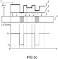
- the Figures 5a to 5c represent an embodiment of the adjustable resistor.
- the adjustable resistor comprises a hybrid structure 1 comprising a first layer of superconducting material 2, a second layer of ferroelectric material 3, a third layer of conductive material 5 and a fourth layer of electrically insulating material 6 disposed between the second 3 and the third layer.
- the first layer of superconducting material 2 advantageously comprises a superconductive material of high critical temperature such as YBCO.
- the superconducting material 2 of critical high temperature can be associated with a small cooling system and low energy consumption.
- the first layer of the first superconducting material 2 extends over a length along an x axis.
- the second layer of ferroelectric material 3 is disposed on the first layer of superconducting material 2.
- the second ferroelectric material 3 has a strong remanent polarization for developing a non-volatile structure.
- the fourth layer of electrically insulating material 6 is disposed on the second layer of the ferroelectric material 3, the thickness of the fourth insulating layer 6 is variable so as to obtain, for the same voltage applied to the third layer of conductive material 5, different electric field values in the second layer of ferroelectric material 3.
- the thickness variations are obtained by cutting the upper face of the fourth layer of material to define a succession of slices, denoted Ti, of length ti, in the hybrid structure 1, along the axis x. According to a variant of the invention, it is possible to make the slices Ti from insulating materials of different dielectric constants.
- a third layer of electrically conductive material 5 is disposed on the upper face of the fourth layer of insulating material 6.
- the third layer of conductive material 5 makes it possible to apply an electrical voltage between the first layer of superconducting material 2 and the third layer of conductive material 5.
- the operating temperature Tf is greater than the first critical temperature TC1.
- the operating temperature Tf corresponds to a temperature for which the difference between the resistances of the first superconductive material 2 in the over-doped and under-doped state is maximum, in particular on the first temperature interval ⁇ T1.
- the figure 5a represents the adjustable resistor as described above at rest, or, in other words, when the direction of polarization is oriented from top to bottom on all the slices Ti of the hybrid structure 1, the direction of polarization of the second ferroelectric material 3 being represented by arrows, and that no electrical voltage is applied between the fourth layer of conductive material 5 and the first layer of superconducting material 2.
- the up-down orientation of the polarization generates a carrier deficit charge in the first layer of superconducting material 2, on all areas opposite the Ti slices, the superconducting material 2 is in the under-doped state.
- the figure 5b represents the adjustable resistance during the imposition of a first voltage U1 using a control means 7.
- the first voltage U1 imposed is equal to the threshold voltage Us, the threshold voltage Us being the voltage required to generate an electric field of intensity equal to the intensity of the reversal electric field Er of the polarization in the absence of the fourth layer of electrically insulating material 6. Due to the different thicknesses of the fourth insulating material 6, the electric fields applied to the second ferroelectric material 3 on the different slices Ti are different.
- the fourth electrically insulating material 6 corresponding to the first slice T1 is relatively thick, the voltage U1 applied between the third layer of conductive material 5 and the first layer of superconducting material 2 produces an electric field in the second ferroelectric material 3 in the slice T1 lower than the electric reversal field Er. As a result, the direction of polarization of the second ferroelectric material 3 corresponding to the first portion T1 is not modified.
- the thickness of the fourth insulating material 6 corresponding to the second wafer T2 being zero, the voltage U1 applied between the third layer of conductive material 5 and the first layer of superconducting material 2 being equal to the voltage Us, and consequently the field on the T2 wafer of the second ferroelectric material 3 is equal to the electric reversal field Er.
- the direction of polarization of the second ferroelectric material 3 corresponding to the second portion T2 is reversed.
- the inverted orientation of the second ferroelectric material 3 is represented by an arrow pointing upwards on the figure 5b . Orientation of the polarization of the second ferroelectric material on the second wafer T2 generates an excess of charge carriers in the first layer of superconducting material 2 on the second wafer T2.
- the first superconducting material 2 is in the overdoped state, with a resistance per unit length pd, represented by a hatched area on the figure 5b .
- the resistance per unit length in the overdoped state pd is less than the resistance per unit length in the underdoped state ps.
- pd is zero if the device is used at a temperature in the temperature range between Tc1 and Tc2.
- the figure 5c represents the adjustable resistance during the application of a second voltage U2, the second voltage U2 being greater than the threshold electrical voltage Us.
- the thickness of the fourth layer of insulating material 6 corresponding to the sixth slice T6 being relatively thin, the voltage applied between the third layer of conductive material 5 and the first layer of superconducting material 2 produces an electric field at least equal to the electric reversal field Er on the sixth slice T6.
- the polarization direction of the second ferroelectric material 3 corresponding to the sixth slice T6 is reversed.
- FIGS. 5a to 5c show an embodiment of the adjustable resistance and highlight the possibility of varying the value of the total resistance by means of an electric control.
- FIGS. 6a to 6f represent a preferred embodiment of the adjustable resistor, according to one aspect of the invention.
- the adjustable resistor comprises a hybrid structure comprising the first superconducting layer 2 of YBCO, the second ferroelectric layer 3 of BFO, the third conductive layer 5 of gold, and the fourth layer of insulating material disposed between the second and the third layer.
- the fourth layer of material forms a ramp in a direction parallel to the x-axis allowing a fine adjustment of the resistance.
- the second ferroelectric layer 3 of BFO may have a thickness of 30 nm.
- the first superconducting layer 2 of YBCO may have a thickness corresponding to 3 units of crystalline mesh.
- the width along the y axis of the hybrid structure may be equal to 10 microns.
- a threshold voltage Us equal to 3V or -3V makes it possible to change the orientation of the polarization of the second ferroelectric layer 3 of BFO when it is directly in contact with the third conductive layer 5 Golden.
- the resistance determined for a hybrid structure 1 as described of the first layer of YBCO in the under-doped state and for a length along the x-axis of 10 ⁇ m is of the order of 2000 ohms.
- the figure 6a represents the hybrid structure at rest, the first ferroelectric layer 3 of BFO is in the over-doped state, the resistance is negligible over the whole of the first superconducting layer 2 of YBCO as indicated by the representative curve of the resistance elementary Ri along the x axis.
- the total resistance R T of the hybrid structure 1 being the sum of the elementary resistances R 1, in this case the total resistance of the hybrid structure 1 is zero.
- the figure 6b represents the hybrid structure when a negative voltage is imposed which is substantially greater than the threshold voltage Us which generates on the ferroelectric layer 3 an electric reversal field Er of the polarization.
- the voltage applied between the third conductive layer 5 of gold and the first superconducting layer 2 of YBCO produces the reversal of the polarization of the ferroelectric layer 3, the first portion corresponds to a zone on which the fourth layer of insulating material 6 has a very thin thickness.
- the first layer of YBCO corresponding to this first portion will pass then from the over-doped state to the under-doped state.
- the resistance of the first portion of the first layer 2 of YBCO is then equal to a resistance Ri.
- the first total resistance R T1 becomes non-zero.
- a second portion of the superconducting layer 2 goes to the under-doped state, as indicated on the Figure 6c .
- the second zone comprising the first zone. It is possible to create a second resistor R T2 , the second total resistor R T2 of the first conductive layer 2 of YBCO being greater than the first total resistor R T1 .
- the figure 6d represents the hybrid structure 1 when a positive voltage substantially greater than the threshold voltage Us is imposed on the hybrid structure 1 as shown in FIG. Figure 6c .
- the voltage applied between the third gold conductive layer and the first YBCO superconducting layer 2 will produce an electric field greater than or equal to the polarization reversal field of the ferroelectric layer 3
- the first layer 2 of YBCO corresponding to this first portion will return from the under-doped state to the over-doped state.
- the resistance of the first portion of the first layer 2 of YBCO is then zero. It is possible to create a third resistor R T3 , the third total resistor R T3 of the first YBCO superconducting layer 2 being smaller than the second total resistor R T2 .
- a third portion of the superconducting layer 2 goes to the over-doped state, as indicated on the figure 6e .
- the third portion comprising the first portion. It is possible to create a fourth resistance R T4 , the fourth total resistance R T4 of the first conducting layer 2 of YBCO being less than the third total resistance R T3 .
- the application of a negative voltage, greater than the threshold voltage Us and greater and larger in absolute value will allow gradually increase the value of the total resistance until reaching a maximum total resistance value. Then, the application of a positive voltage, greater than the threshold voltage Us and increasingly large will gradually decrease the value of the total resistance until reaching a zero total resistance value.
- the proposed device makes it possible to achieve an adjustable resistance by electrical control, the resistance retaining its value even after stopping the application of the control voltage.
Landscapes
- Engineering & Computer Science (AREA)
- Computer Hardware Design (AREA)
- Chemical & Material Sciences (AREA)
- Microelectronics & Electronic Packaging (AREA)
- Molecular Biology (AREA)
- General Health & Medical Sciences (AREA)
- Biomedical Technology (AREA)
- Neurology (AREA)
- Life Sciences & Earth Sciences (AREA)
- Health & Medical Sciences (AREA)
- Materials Engineering (AREA)
- Physics & Mathematics (AREA)
- Electromagnetism (AREA)
- Ceramic Engineering (AREA)
- Superconductor Devices And Manufacturing Methods Thereof (AREA)
Claims (5)
- Elektrischer Speichereffektwiderstand, der durch elektrische Steuerung justierbar ist und Folgendes umfasst:• einen Stapel, der Folgendes umfasst:- eine erste Schicht aus einem ersten supraleitenden Material (2) mit einem ersten unterdotierten Zustand mit einer ersten kritischen Temperatur (Tc1) und einem zweiten überdotierten Zustand mit einer zweiten kritischen Temperatur (Tc2), wobei die zweite kritische Temperatur (Tc2) höher ist als die erste kritische Temperatur (Tc1), wobei die erste Schicht aus supraleitendem Material (2) entlang einer x-Achse verläuft;- eine zweite Schicht aus einem zweiten ferroelektrischen Material (3), das polarisiert ist oder eine Komponente seiner Polarisation in einer Richtung parallel zur Richtung des Stapels hat, wobei der Zustand des ersten Materials (2) von der Polarisationsrichtung des zweiten Materials (3) abhängt; und- eine dritte Schicht aus einem dritten leitenden Material (5);• ein Mittel (7) zum Regeln der elektrischen Spannung zwischen der ersten Schicht aus supraleitendem Material (2) und der dritten Schicht aus leitendem Material (5) zum Erzeugen eines elektrischen Feldes, das die Modifikation der Polarisationsrichtung des zweiten ferroelektrischen Materials (3) zulässt, wenn die elektrische Steuerspannung höher ist als ein Schwellenspannungswert (Us),wobei das zweite ferroelektrische Material (3) die Polarisationsrichtung behält, die durch das Anlegen der elektrischen Spannung nach dem Stoppen des Anlegens der elektrischen Spannung definiert wird,
dadurch gekennzeichnet, dass der Stapel ferner eine vierte Schicht umfasst, die wenigstens ein viertes elektrisches isolierendes Material (6) umfasst, wobei die vierte Schicht (6) zwischen der zweiten Schicht aus ferroelektrischem Material (3) und der dritten Schicht aus leitendem Material (5) angeordnet ist, wobei die Dicke der vierten elektrisch isolierenden Schicht (6) in einer Richtung parallel zur x-Achse variiert, und/oder die vierte Schicht eine Folge von Materialien mit einer anderen Dielektrizitätskonstante in einer Richtung parallel zur x-Achse umfasst, um das zwischen der ersten Schicht (2) und der dritten Schicht (5) angelegte elektrische Feld zu varüeren, wobei der justierbare Widerstand zum Arbeiten über ein Temperaturintervall konfiguriert ist, in dem die Abweichung des elektrischen Widerstands zwischen dem überdotierten Zustand und dem unterdotierten Zustand des ersten Materials ungleich null ist. - Justierbarer Widerstand nach Anspruch 1, wobei die Dicke der vierten elektrisch isolierenden Schicht (6) in einer Richtung parallel zur x-Achse kontinuierlich zunimmt.
- Justierbarer Widerstand nach einem der vorherigen Ansprüche, wobei das erste Material (2) ein Supraleiter mit hoher kritischer Temperatur ist.
- Justierbarer Widerstand nach Anspruch 3, wobei das erste supraleitende Material (2) YBa2Cu3O7-x oder NdBa2Cu3O7-x oder ein beliebiges anderes supraleitendes Material aus der Familie der ReBa2CuO7-x umfasst, wobei Re ein Material aus der Seltenerdfamilie oder ein beliebiges anderes supraleitendes Material aus der Cupratfamilie ist.
- Justierbarer Widerstand nach Anspruch 4, wobei das zweite Material (3) BiFeO3 oder BaTiO3 umfasst.
Applications Claiming Priority (2)
| Application Number | Priority Date | Filing Date | Title |
|---|---|---|---|
| FR1203321A FR2999328B1 (fr) | 2012-12-07 | 2012-12-07 | Resistance reglable |
| PCT/EP2013/075840 WO2014086990A1 (fr) | 2012-12-07 | 2013-12-06 | Resistance reglable |
Publications (3)
| Publication Number | Publication Date |
|---|---|
| EP2929535A1 EP2929535A1 (de) | 2015-10-14 |
| EP2929535B1 true EP2929535B1 (de) | 2017-09-20 |
| EP2929535B8 EP2929535B8 (de) | 2017-10-25 |
Family
ID=48170520
Family Applications (1)
| Application Number | Title | Priority Date | Filing Date |
|---|---|---|---|
| EP13801586.2A Active EP2929535B8 (de) | 2012-12-07 | 2013-12-06 | Varisator |
Country Status (4)
| Country | Link |
|---|---|
| US (1) | US9412504B2 (de) |
| EP (1) | EP2929535B8 (de) |
| FR (1) | FR2999328B1 (de) |
| WO (1) | WO2014086990A1 (de) |
Families Citing this family (1)
| Publication number | Priority date | Publication date | Assignee | Title |
|---|---|---|---|---|
| WO2021053682A1 (en) * | 2019-09-22 | 2021-03-25 | Technion Research & Development Foundation Limited | Superconductor composites and devices comprising same |
Family Cites Families (4)
| Publication number | Priority date | Publication date | Assignee | Title |
|---|---|---|---|---|
| JPH06169112A (ja) * | 1992-12-01 | 1994-06-14 | Matsushita Electric Ind Co Ltd | 超伝導素子およびその製造方法 |
| US20020180006A1 (en) * | 2001-05-31 | 2002-12-05 | Marcel Franz | Ferroelectric-superconductor heterostructures in solid state quantum computing systems |
| US20090163656A1 (en) * | 2007-12-21 | 2009-06-25 | Envont Llc | Hybrid vehicle systems |
| FR2954855B1 (fr) * | 2009-12-30 | 2012-09-28 | Thales Sa | Circuit a jonctions josephson a structure hybride supraconducteur/ferroelectrique |
-
2012
- 2012-12-07 FR FR1203321A patent/FR2999328B1/fr not_active Expired - Fee Related
-
2013
- 2013-12-06 EP EP13801586.2A patent/EP2929535B8/de active Active
- 2013-12-06 US US14/649,887 patent/US9412504B2/en active Active
- 2013-12-06 WO PCT/EP2013/075840 patent/WO2014086990A1/fr not_active Ceased
Non-Patent Citations (1)
| Title |
|---|
| None * |
Also Published As
| Publication number | Publication date |
|---|---|
| US20150302956A1 (en) | 2015-10-22 |
| FR2999328A1 (fr) | 2014-06-13 |
| WO2014086990A1 (fr) | 2014-06-12 |
| EP2929535A1 (de) | 2015-10-14 |
| US9412504B2 (en) | 2016-08-09 |
| EP2929535B8 (de) | 2017-10-25 |
| FR2999328B1 (fr) | 2015-02-06 |
Similar Documents
| Publication | Publication Date | Title |
|---|---|---|
| CA2095964C (fr) | Capteur a effect hall | |
| EP2294637A1 (de) | Feldeffekt-supraleitertransistor und verfahren zur herstellung eines solchen transistors | |
| EP1430484A2 (de) | Magnetische speicheranordnung beschreibbar durch spin-polarisierten strom unter benützung von amorphen ferrimagnetischen legierungen, und schreibverfahren in dieser speicheranordnung | |
| EP3171404A1 (de) | Optoelektronische vorrichtung mit leuchtdioden, die mindestens eine zener-diode umfassen | |
| EP1604220A1 (de) | Magnetoresistiver wandler mit einem ferromagnetischen/antiferromagnetischen fühlelement | |
| Copel et al. | Giant piezoresistive On/Off ratios in rare-earth chalcogenide thin films enabling nanomechanical switching | |
| FR2969382A1 (fr) | Élément memristif et mémoire électronique basée sur de tels éléments | |
| FR2586804A1 (fr) | Procede et dispositif de photo-detection rapide a l'aide d'un superreseau | |
| Jung et al. | Unipolar resistive switching in insulating niobium oxide film and probing electroforming induced metallic components | |
| EP2929535B1 (de) | Varisator | |
| EP2875529B1 (de) | Vorrichtung mit einer vielzahl von dünnen schichten | |
| EP1419506B1 (de) | Steuereinrichtung zur umkehr der magnetisierungsrichtung ohne ein externes magnetfeld | |
| EP2107623B1 (de) | Magnetvorrichtung, die einen magnetoresistiven Stapel und mindestens einen Nanokontakt umfasst | |
| EP2945160B1 (de) | Elektronische komponente mit josephson-kontakt | |
| FR3071667A1 (fr) | Couche composite de dopage electrostatique d'une couche bidimensionnelle dopee, capteur hall, procede et dispositif pour la realisation d'une telle couche composite | |
| Chikanari et al. | Enhancement of electronic-transport switching in single-crystal narrower VO2 nanowire channels through side-gate electric fields | |
| US20130234103A1 (en) | Nanoscale switching device with an amorphous switching material | |
| FR2954855A1 (fr) | Circuit a jonctions josephson a structure hybride supraconducteur/ferroelectrique | |
| EP3510598B1 (de) | Vorrichtung zur auswahl einer speicherzelle | |
| Seyidov et al. | Field induced rectification and memristive behavior of TlGaSe2 layered semiconductor | |
| EP3143694B1 (de) | Spintronic logikschaltung mit spin polarisiertem stromschalter und integrierter schaltung | |
| EP3459125B1 (de) | Vorrichtung mit einem josephson-übergang | |
| WO2011025506A1 (en) | Low-power nanoscale switching device with an amorphous switching material | |
| FR3160515A1 (fr) | Circuit électronique reconfigurable et procédés associés | |
| FR3058831B1 (fr) | Composant electronique a heterojonction a haute mobilite electronique |
Legal Events
| Date | Code | Title | Description |
|---|---|---|---|
| PUAI | Public reference made under article 153(3) epc to a published international application that has entered the european phase |
Free format text: ORIGINAL CODE: 0009012 |
|
| 17P | Request for examination filed |
Effective date: 20150604 |
|
| AK | Designated contracting states |
Kind code of ref document: A1 Designated state(s): AL AT BE BG CH CY CZ DE DK EE ES FI FR GB GR HR HU IE IS IT LI LT LU LV MC MK MT NL NO PL PT RO RS SE SI SK SM TR |
|
| AX | Request for extension of the european patent |
Extension state: BA ME |
|
| DAX | Request for extension of the european patent (deleted) | ||
| GRAP | Despatch of communication of intention to grant a patent |
Free format text: ORIGINAL CODE: EPIDOSNIGR1 |
|
| RIC1 | Information provided on ipc code assigned before grant |
Ipc: G11C 13/00 20060101ALI20170210BHEP Ipc: H01L 39/22 20060101ALI20170210BHEP Ipc: H01C 7/10 20060101ALI20170210BHEP Ipc: G11C 11/54 20060101ALI20170210BHEP Ipc: H01L 27/18 20060101ALI20170210BHEP Ipc: G11C 11/56 20060101ALI20170210BHEP Ipc: G11C 11/44 20060101ALI20170210BHEP Ipc: G11C 11/22 20060101AFI20170210BHEP Ipc: H01L 45/00 20060101ALI20170210BHEP |
|
| INTG | Intention to grant announced |
Effective date: 20170227 |
|
| GRAS | Grant fee paid |
Free format text: ORIGINAL CODE: EPIDOSNIGR3 |
|
| GRAA | (expected) grant |
Free format text: ORIGINAL CODE: 0009210 |
|
| GRAT | Correction requested after decision to grant or after decision to maintain patent in amended form |
Free format text: ORIGINAL CODE: EPIDOSNCDEC |
|
| RAP1 | Party data changed (applicant data changed or rights of an application transferred) |
Owner name: CNRS (CENTRE NATIONAL DE LA RECHERCHE SCIENTIFIQUE Owner name: THALES |
|
| AK | Designated contracting states |
Kind code of ref document: B1 Designated state(s): AL AT BE BG CH CY CZ DE DK EE ES FI FR GB GR HR HU IE IS IT LI LT LU LV MC MK MT NL NO PL PT RO RS SE SI SK SM TR |
|
| REG | Reference to a national code |
Ref country code: GB Ref legal event code: FG4D Free format text: NOT ENGLISH |
|
| REG | Reference to a national code |
Ref country code: CH Ref legal event code: EP |
|
| RAP2 | Party data changed (patent owner data changed or rights of a patent transferred) |
Owner name: CENTRE NATIONAL DE LA RECHERCHE SCIENTIFIQUE Owner name: THALES |
|
| REG | Reference to a national code |
Ref country code: AT Ref legal event code: REF Ref document number: 930747 Country of ref document: AT Kind code of ref document: T Effective date: 20171015 |
|
| REG | Reference to a national code |
Ref country code: IE Ref legal event code: FG4D Free format text: LANGUAGE OF EP DOCUMENT: FRENCH |
|
| REG | Reference to a national code |
Ref country code: DE Ref legal event code: R096 Ref document number: 602013026925 Country of ref document: DE |
|
| REG | Reference to a national code |
Ref country code: FR Ref legal event code: PLFP Year of fee payment: 5 |
|
| REG | Reference to a national code |
Ref country code: NL Ref legal event code: FP |
|
| PG25 | Lapsed in a contracting state [announced via postgrant information from national office to epo] |
Ref country code: SE Free format text: LAPSE BECAUSE OF FAILURE TO SUBMIT A TRANSLATION OF THE DESCRIPTION OR TO PAY THE FEE WITHIN THE PRESCRIBED TIME-LIMIT Effective date: 20170920 Ref country code: HR Free format text: LAPSE BECAUSE OF FAILURE TO SUBMIT A TRANSLATION OF THE DESCRIPTION OR TO PAY THE FEE WITHIN THE PRESCRIBED TIME-LIMIT Effective date: 20170920 Ref country code: LT Free format text: LAPSE BECAUSE OF FAILURE TO SUBMIT A TRANSLATION OF THE DESCRIPTION OR TO PAY THE FEE WITHIN THE PRESCRIBED TIME-LIMIT Effective date: 20170920 Ref country code: NO Free format text: LAPSE BECAUSE OF FAILURE TO SUBMIT A TRANSLATION OF THE DESCRIPTION OR TO PAY THE FEE WITHIN THE PRESCRIBED TIME-LIMIT Effective date: 20171220 Ref country code: FI Free format text: LAPSE BECAUSE OF FAILURE TO SUBMIT A TRANSLATION OF THE DESCRIPTION OR TO PAY THE FEE WITHIN THE PRESCRIBED TIME-LIMIT Effective date: 20170920 |
|
| REG | Reference to a national code |
Ref country code: LT Ref legal event code: MG4D |
|
| REG | Reference to a national code |
Ref country code: AT Ref legal event code: MK05 Ref document number: 930747 Country of ref document: AT Kind code of ref document: T Effective date: 20170920 |
|
| PG25 | Lapsed in a contracting state [announced via postgrant information from national office to epo] |
Ref country code: GR Free format text: LAPSE BECAUSE OF FAILURE TO SUBMIT A TRANSLATION OF THE DESCRIPTION OR TO PAY THE FEE WITHIN THE PRESCRIBED TIME-LIMIT Effective date: 20171221 Ref country code: BG Free format text: LAPSE BECAUSE OF FAILURE TO SUBMIT A TRANSLATION OF THE DESCRIPTION OR TO PAY THE FEE WITHIN THE PRESCRIBED TIME-LIMIT Effective date: 20171220 Ref country code: LV Free format text: LAPSE BECAUSE OF FAILURE TO SUBMIT A TRANSLATION OF THE DESCRIPTION OR TO PAY THE FEE WITHIN THE PRESCRIBED TIME-LIMIT Effective date: 20170920 Ref country code: RS Free format text: LAPSE BECAUSE OF FAILURE TO SUBMIT A TRANSLATION OF THE DESCRIPTION OR TO PAY THE FEE WITHIN THE PRESCRIBED TIME-LIMIT Effective date: 20170920 |
|
| PG25 | Lapsed in a contracting state [announced via postgrant information from national office to epo] |
Ref country code: ES Free format text: LAPSE BECAUSE OF FAILURE TO SUBMIT A TRANSLATION OF THE DESCRIPTION OR TO PAY THE FEE WITHIN THE PRESCRIBED TIME-LIMIT Effective date: 20170920 Ref country code: CZ Free format text: LAPSE BECAUSE OF FAILURE TO SUBMIT A TRANSLATION OF THE DESCRIPTION OR TO PAY THE FEE WITHIN THE PRESCRIBED TIME-LIMIT Effective date: 20170920 Ref country code: RO Free format text: LAPSE BECAUSE OF FAILURE TO SUBMIT A TRANSLATION OF THE DESCRIPTION OR TO PAY THE FEE WITHIN THE PRESCRIBED TIME-LIMIT Effective date: 20170920 Ref country code: PL Free format text: LAPSE BECAUSE OF FAILURE TO SUBMIT A TRANSLATION OF THE DESCRIPTION OR TO PAY THE FEE WITHIN THE PRESCRIBED TIME-LIMIT Effective date: 20170920 |
|
| PG25 | Lapsed in a contracting state [announced via postgrant information from national office to epo] |
Ref country code: SK Free format text: LAPSE BECAUSE OF FAILURE TO SUBMIT A TRANSLATION OF THE DESCRIPTION OR TO PAY THE FEE WITHIN THE PRESCRIBED TIME-LIMIT Effective date: 20170920 Ref country code: SM Free format text: LAPSE BECAUSE OF FAILURE TO SUBMIT A TRANSLATION OF THE DESCRIPTION OR TO PAY THE FEE WITHIN THE PRESCRIBED TIME-LIMIT Effective date: 20170920 Ref country code: IS Free format text: LAPSE BECAUSE OF FAILURE TO SUBMIT A TRANSLATION OF THE DESCRIPTION OR TO PAY THE FEE WITHIN THE PRESCRIBED TIME-LIMIT Effective date: 20180120 Ref country code: IT Free format text: LAPSE BECAUSE OF FAILURE TO SUBMIT A TRANSLATION OF THE DESCRIPTION OR TO PAY THE FEE WITHIN THE PRESCRIBED TIME-LIMIT Effective date: 20170920 Ref country code: AT Free format text: LAPSE BECAUSE OF FAILURE TO SUBMIT A TRANSLATION OF THE DESCRIPTION OR TO PAY THE FEE WITHIN THE PRESCRIBED TIME-LIMIT Effective date: 20170920 Ref country code: EE Free format text: LAPSE BECAUSE OF FAILURE TO SUBMIT A TRANSLATION OF THE DESCRIPTION OR TO PAY THE FEE WITHIN THE PRESCRIBED TIME-LIMIT Effective date: 20170920 |
|
| REG | Reference to a national code |
Ref country code: DE Ref legal event code: R097 Ref document number: 602013026925 Country of ref document: DE |
|
| PLBE | No opposition filed within time limit |
Free format text: ORIGINAL CODE: 0009261 |
|
| STAA | Information on the status of an ep patent application or granted ep patent |
Free format text: STATUS: NO OPPOSITION FILED WITHIN TIME LIMIT |
|
| PG25 | Lapsed in a contracting state [announced via postgrant information from national office to epo] |
Ref country code: DK Free format text: LAPSE BECAUSE OF FAILURE TO SUBMIT A TRANSLATION OF THE DESCRIPTION OR TO PAY THE FEE WITHIN THE PRESCRIBED TIME-LIMIT Effective date: 20170920 |
|
| REG | Reference to a national code |
Ref country code: CH Ref legal event code: PL |
|
| 26N | No opposition filed |
Effective date: 20180621 |
|
| GBPC | Gb: european patent ceased through non-payment of renewal fee |
Effective date: 20171220 |
|
| REG | Reference to a national code |
Ref country code: IE Ref legal event code: MM4A |
|
| PG25 | Lapsed in a contracting state [announced via postgrant information from national office to epo] |
Ref country code: LU Free format text: LAPSE BECAUSE OF NON-PAYMENT OF DUE FEES Effective date: 20171206 Ref country code: MT Free format text: LAPSE BECAUSE OF FAILURE TO SUBMIT A TRANSLATION OF THE DESCRIPTION OR TO PAY THE FEE WITHIN THE PRESCRIBED TIME-LIMIT Effective date: 20170920 |
|
| REG | Reference to a national code |
Ref country code: BE Ref legal event code: MM Effective date: 20171231 |
|
| PG25 | Lapsed in a contracting state [announced via postgrant information from national office to epo] |
Ref country code: IE Free format text: LAPSE BECAUSE OF NON-PAYMENT OF DUE FEES Effective date: 20171206 |
|
| PG25 | Lapsed in a contracting state [announced via postgrant information from national office to epo] |
Ref country code: CH Free format text: LAPSE BECAUSE OF NON-PAYMENT OF DUE FEES Effective date: 20171231 Ref country code: SI Free format text: LAPSE BECAUSE OF FAILURE TO SUBMIT A TRANSLATION OF THE DESCRIPTION OR TO PAY THE FEE WITHIN THE PRESCRIBED TIME-LIMIT Effective date: 20170920 Ref country code: LI Free format text: LAPSE BECAUSE OF NON-PAYMENT OF DUE FEES Effective date: 20171231 Ref country code: GB Free format text: LAPSE BECAUSE OF NON-PAYMENT OF DUE FEES Effective date: 20171220 Ref country code: BE Free format text: LAPSE BECAUSE OF NON-PAYMENT OF DUE FEES Effective date: 20171231 |
|
| PG25 | Lapsed in a contracting state [announced via postgrant information from national office to epo] |
Ref country code: HU Free format text: LAPSE BECAUSE OF FAILURE TO SUBMIT A TRANSLATION OF THE DESCRIPTION OR TO PAY THE FEE WITHIN THE PRESCRIBED TIME-LIMIT; INVALID AB INITIO Effective date: 20131206 Ref country code: MC Free format text: LAPSE BECAUSE OF FAILURE TO SUBMIT A TRANSLATION OF THE DESCRIPTION OR TO PAY THE FEE WITHIN THE PRESCRIBED TIME-LIMIT Effective date: 20170920 |
|
| PG25 | Lapsed in a contracting state [announced via postgrant information from national office to epo] |
Ref country code: CY Free format text: LAPSE BECAUSE OF FAILURE TO SUBMIT A TRANSLATION OF THE DESCRIPTION OR TO PAY THE FEE WITHIN THE PRESCRIBED TIME-LIMIT Effective date: 20170920 |
|
| PG25 | Lapsed in a contracting state [announced via postgrant information from national office to epo] |
Ref country code: MK Free format text: LAPSE BECAUSE OF FAILURE TO SUBMIT A TRANSLATION OF THE DESCRIPTION OR TO PAY THE FEE WITHIN THE PRESCRIBED TIME-LIMIT Effective date: 20170920 |
|
| PG25 | Lapsed in a contracting state [announced via postgrant information from national office to epo] |
Ref country code: TR Free format text: LAPSE BECAUSE OF FAILURE TO SUBMIT A TRANSLATION OF THE DESCRIPTION OR TO PAY THE FEE WITHIN THE PRESCRIBED TIME-LIMIT Effective date: 20170920 |
|
| PG25 | Lapsed in a contracting state [announced via postgrant information from national office to epo] |
Ref country code: PT Free format text: LAPSE BECAUSE OF FAILURE TO SUBMIT A TRANSLATION OF THE DESCRIPTION OR TO PAY THE FEE WITHIN THE PRESCRIBED TIME-LIMIT Effective date: 20170920 |
|
| PG25 | Lapsed in a contracting state [announced via postgrant information from national office to epo] |
Ref country code: AL Free format text: LAPSE BECAUSE OF FAILURE TO SUBMIT A TRANSLATION OF THE DESCRIPTION OR TO PAY THE FEE WITHIN THE PRESCRIBED TIME-LIMIT Effective date: 20170920 |
|
| PGFP | Annual fee paid to national office [announced via postgrant information from national office to epo] |
Ref country code: NL Payment date: 20241128 Year of fee payment: 12 |
|
| PGFP | Annual fee paid to national office [announced via postgrant information from national office to epo] |
Ref country code: DE Payment date: 20241120 Year of fee payment: 12 |
|
| PGFP | Annual fee paid to national office [announced via postgrant information from national office to epo] |
Ref country code: FR Payment date: 20241121 Year of fee payment: 12 |