EP2933757A1 - Kommunikationsvorrichtung, kommunikationsverfahren, integrierte schaltung und elektronisches instrument - Google Patents
Kommunikationsvorrichtung, kommunikationsverfahren, integrierte schaltung und elektronisches instrument Download PDFInfo
- Publication number
- EP2933757A1 EP2933757A1 EP13863384.7A EP13863384A EP2933757A1 EP 2933757 A1 EP2933757 A1 EP 2933757A1 EP 13863384 A EP13863384 A EP 13863384A EP 2933757 A1 EP2933757 A1 EP 2933757A1
- Authority
- EP
- European Patent Office
- Prior art keywords
- circuit
- transmission data
- transmitting
- antenna
- unit
- Prior art date
- Legal status (The legal status is an assumption and is not a legal conclusion. Google has not performed a legal analysis and makes no representation as to the accuracy of the status listed.)
- Granted
Links
Images





Classifications
-
- H—ELECTRICITY
- H04—ELECTRIC COMMUNICATION TECHNIQUE
- H04B—TRANSMISSION
- H04B5/00—Near-field transmission systems, e.g. inductive or capacitive transmission systems
- H04B5/70—Near-field transmission systems, e.g. inductive or capacitive transmission systems specially adapted for specific purposes
- H04B5/77—Near-field transmission systems, e.g. inductive or capacitive transmission systems specially adapted for specific purposes for interrogation
-
- G—PHYSICS
- G06—COMPUTING OR CALCULATING; COUNTING
- G06K—GRAPHICAL DATA READING; PRESENTATION OF DATA; RECORD CARRIERS; HANDLING RECORD CARRIERS
- G06K7/00—Methods or arrangements for sensing record carriers, e.g. for reading patterns
- G06K7/10—Methods or arrangements for sensing record carriers, e.g. for reading patterns by electromagnetic radiation, e.g. optical sensing; by corpuscular radiation
- G06K7/10009—Methods or arrangements for sensing record carriers, e.g. for reading patterns by electromagnetic radiation, e.g. optical sensing; by corpuscular radiation sensing by radiation using wavelengths larger than 0.1 mm, e.g. radio-waves or microwaves
- G06K7/10297—Methods or arrangements for sensing record carriers, e.g. for reading patterns by electromagnetic radiation, e.g. optical sensing; by corpuscular radiation sensing by radiation using wavelengths larger than 0.1 mm, e.g. radio-waves or microwaves arrangements for handling protocols designed for non-contact record carriers such as RFIDs NFCs, e.g. ISO/IEC 14443 and 18092
-
- G—PHYSICS
- G06—COMPUTING OR CALCULATING; COUNTING
- G06K—GRAPHICAL DATA READING; PRESENTATION OF DATA; RECORD CARRIERS; HANDLING RECORD CARRIERS
- G06K7/00—Methods or arrangements for sensing record carriers, e.g. for reading patterns
- G06K7/10—Methods or arrangements for sensing record carriers, e.g. for reading patterns by electromagnetic radiation, e.g. optical sensing; by corpuscular radiation
- G06K7/10009—Methods or arrangements for sensing record carriers, e.g. for reading patterns by electromagnetic radiation, e.g. optical sensing; by corpuscular radiation sensing by radiation using wavelengths larger than 0.1 mm, e.g. radio-waves or microwaves
- G06K7/10366—Methods or arrangements for sensing record carriers, e.g. for reading patterns by electromagnetic radiation, e.g. optical sensing; by corpuscular radiation sensing by radiation using wavelengths larger than 0.1 mm, e.g. radio-waves or microwaves the interrogation device being adapted for miscellaneous applications
-
- H—ELECTRICITY
- H04—ELECTRIC COMMUNICATION TECHNIQUE
- H04B—TRANSMISSION
- H04B5/00—Near-field transmission systems, e.g. inductive or capacitive transmission systems
- H04B5/20—Near-field transmission systems, e.g. inductive or capacitive transmission systems characterised by the transmission technique; characterised by the transmission medium
- H04B5/24—Inductive coupling
- H04B5/26—Inductive coupling using coils
Definitions
- the present technology relates to a communication device, a communication method, an integrated circuit, and an electronic instrument, and more particularly, to a communication device, a communication method, an integrated circuit, and an electronic instrument, which are capable of reducing a manufacturing cost.
- an RF tag includes an antenna therein, and performs near field communication with a dedicated reader/writer using a weak radio wave.
- RF tags there is an RF tag having a function of a reader/writer communicating with another RF tag as well as a function of an RF tag communicating with a dedicated reader/writer.
- Such an RF tag operates as an RF tag or a reader/writer according to a use state.
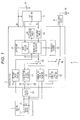
- Fig. 1 illustrates a configuration of a communication device 1 having both functions of an RF tag and a reader/writer.
- the communication device 1 includes an antenna circuit 11, an integrated circuit 12, a host controller 13, a power source 14, an oscillating circuit 15, and a crystal oscillator 16.
- the antenna circuit 11 includes a coil 31 and a capacitor 32 and forms a parallel resonant circuit.
- the power source 14 supplies the integrated circuit 12 and the host controller 13 with electric power.
- the oscillating circuit 15 generates a carrier of a frequency (13.56 MHz) corresponding to a vibration frequency of the crystal oscillator 16.
- the integrated circuit 12 modulates transmission data according to control of the host controller 13, and transmits a modulated signal obtained by the modulating to a communication destination through the antenna circuit 11. Further, the integrated circuit 12 receives a modulated signal from a communication destination through the antenna circuit 11 according to control of the host controller 13, and demodulates the modulated signal.
- the integrated circuit 12 includes a control unit 51 that controls respective units, a non-volatile memory 52 that appropriately stores various kinds of data, a data input circuit 53 that receives transmission data, and a data output circuit 54 that outputs reception data.
- the control unit 51 includes a mode control unit 71 and a communication control unit 72.
- the mode control unit 71 controls switching operations of a switch 55 and a switch 56 according to control of the host controller 13.
- the communication control unit 72 not only controls an input and output of the transmission data and the reception data but also performs various kinds of processes on the data.
- an operation mode of the communication device 1 includes a reader/writer mode in which the communication device 1 operates as a reader/writer and a tag mode in which the communication device 1 operates as an RF tag.
- the integrated circuit 12 is provided with a transmitting circuit 57 serving as a circuit for a reader/writer function, a transmitting circuit 61 serving as a circuit for an RF tag function, and a receiving circuit 63 serving as a circuit for both functions.
- the transmitting circuit 57 When an operation is performed the reader/writer mode, the transmitting circuit 57 performs Amplitude Shift Keying (ASK) (hereinafter, referred to as an "ASK modulation") on the transmission data supplied from the communication control unit 72 according to a carrier generated by the oscillating circuit 15.
- ASK modulation Amplitude Shift Keying
- transmitting buffer circuits 58 and 59 are provided so that the carrier can be driven at the low impedance.
- the modulated signal obtained by the ASK modulation is transmitted to the RF tag of the communication destination through a filter circuit 60 and the antenna circuit 11.
- the transmitting circuit 61 When an operation is performed in the tag mode, the transmitting circuit 61 performs load modulation on reply transmission data supplied from the communication control unit 72 according to a clock signal extracted by a clock extracting circuit 62, and applies the modulated data to the coil 31 of the antenna circuit 11. As a result, the reply transmission data is transmitted to the reader/writer of the communication destination.
- the receiving circuit 63 is a circuit that is used in both operation modes of the reader/writer mode and the tag mode. When an operation is performed in the tag mode or the reader/writer mode, the receiving circuit 63 receives a modulated signal transmitted from a communication destination through the antenna circuit 11 and the filter circuit 60, demodulates the modulated signal, and supplies reception data obtained by the demodulating to the communication control unit 72.
- the communication device 1 is configured to have both functions of the RF tag and the reader/writer.
- Patent Document 1 JP 4797991 B1
- a modulation scheme in the case where the communication device 1 operates as the reader/writer is different from that in the case where the communication device 1 operates as the RF tag, and thus it is necessary to install a plurality of transmitting circuits according to the modulation schemes.
- the ASK modulation is used as the modulation scheme when the communication device 1 operates as the reader/writer
- the load modulation is used as the modulation scheme when the communication device 1 operates as the RF tag, and thus it is necessary to install the transmitting circuit 57 for the reader/writer function and the transmitting circuit 61 for the RF tag function separately. For this reason, there is a demand for commonalizing the dedicated transmitting circuits and reducing a manufacturing cost.
- the present technology was made in light of the foregoing, and it is desirable to reduce a manufacturing cost of a communication device having both functions of an RF tag and reader/writer or an electronic instrument including the communication device.
- a communication device includes: an antenna unit; a transmitting unit that modulates transmission data, and transmits the transmission data to a communication destination through the antenna unit; and a receiving unit that receives modulated reception data from the communication destination through the antenna unit, and demodulates the modulated reception data, wherein the transmitting unit and the receiving unit operate in any one of a first operation mode in which an operation of a radio frequency identification (RFID) reader/writer is performed and a second operation mode in which an operation of a communication target of the RFID reader/writer is performed, the transmitting unit transmits the transmission data to the communication target by performing load modulation of changing an impedance of the antenna unit according to the transmission data using a first carrier generated in the antenna unit when the transmitting unit operates in the first operation mode, and the transmitting unit transmits the transmission data to the RFID reader/writer by performing the load modulation of changing the impedance of the antenna unit according to the transmission data using a second carrier received by the antenna unit when the transmitting unit operates in the second operation mode.
- RFID radio frequency identification
- the communication device further includes a carrier generating unit that generates the first carrier.
- the carrier generating unit causes the impedance of the antenna unit to have a value of a predetermined magnitude.
- the first carrier is generated by an external carrier generating device.
- the transmission data and the reception data are encoded by the same coding scheme.
- the communication device further includes a voltage setting unit that restricts a power voltage generated by electromagnetic induction of the antenna unit according to the operation mode.
- the communication device may be an independent device or may be an internal block configuring a single device.
- a communication method and an electronic instrument according to an aspect of the present technology are a communication method and an electronic instrument corresponding to the communication device according to an aspect of the present technology.
- An integrated circuit includes: a transmitting circuit that modulates transmission data, and transmits the transmission data to a communication destination through an external antenna circuit; and a receiving circuit that receives modulated reception data from the communication destination through the antenna circuit, and demodulates the modulated reception data, wherein the transmitting circuit and the receiving circuit operate in any one of a first operation mode in which an operation of an RFID reader/writer is performed and a second operation mode in which an operation of a communication target of the RFID reader/writer is performed, the transmitting circuit transmits the transmission data to the communication target by performing load modulation of changing an impedance of the antenna circuit according to the transmission data using a first carrier generated in the antenna circuit when the transmitting circuit operates in the first operation mode, and the transmitting circuit transmits the transmission data to the RFID reader/writer by performing the load modulation of changing the impedance of the antenna circuit according to the transmission data using a second carrier received by the antenna circuit when the transmitting circuit operates in the second operation mode.
- the first carrier is generated by an external carrier generating circuit.
- the carrier generating circuit causes the impedance of the antenna circuit to have a value of a predetermined magnitude.
- the transmission data and the reception data are encoded by the same coding scheme.
- the integrated circuit further includes a voltage setting circuit that restricts a power voltage generated by electromagnetic induction of the antenna circuit according to the operation mode.
- a communication method according to an aspect of the present technology is a communication method corresponding to the integrated circuit according to an aspect of the present technology.
- the transmission data is transmitted to the communication target by performing the load modulation of changing the impedance of the antenna unit according to the transmission data using the first carrier generated in the antenna unit when the operation is performed in the first operation mode
- the transmission data is transmitted to the RFID reader/writer by performing the load modulation of changing the impedance of the antenna unit according to the transmission data using the second carrier received by the antenna unit when the operation is performed in the second operation mode.
- Fig. 2 is a diagram illustrating a configuration of a communication device according to an embodiment of the present technology.
- a communication device 101 includes an antenna circuit 111, an integrated circuit 112, a host controller 113, a power source 114, and an external circuit 115.
- the antenna circuit 111 includes a coil 131 and a capacitor 132 that perform a parallel resonant circuit.
- L11 indicates inductance of the coil 131
- C11 indicates capacitance of the capacitor 132.
- the antenna circuit 111 is adjusted to an inductor value at which a magnetic field of 13.56 MHz can be efficiently received, and an effect thereof can be increased by a variable capacitor.
- the integrated circuit 112 is a circuit having both functions of an RF tag and a reader/writer and configured as a so-called IC chip.
- the integrated circuit 112 modulates input transmission data according to control of the host controller 113, and transmits a modulated signal obtained by the modulating to a communication destination through the antenna circuit 111.
- the integrated circuit 112 receives a modulated signal transmitted from a communication destination through the antenna circuit 111 according to control of the host controller 113, demodulates the modulated signal, and outputs reception data obtained by the demodulating.
- the host controller 113 controls operations of the respective units of the communication device 101. Specifically, the host controller 113 supplies a control signal (MODE) or a transmission data (TX) to the integrated circuit 112 according to an operation state of the communication device 101, and supplies a control signal (EN) to the external circuit 115. The host controller 113 acquires reception data (RX) supplied from the integrated circuit 112, and performs various kinds of processes.
- a control signal MODE
- TX transmission data
- EN control signal
- the power source 114 supplies a power voltage (VDD) to the integrated circuit 112, the host controller 113, and the external circuit 115 as a DC voltage necessary for operating the respective circuits.
- VDD power voltage
- the external circuit 115 When the communication device 101 operates in a reader/writer mode which will be described later, the external circuit 115 generates a carrier (a carrier wave) of a predetermined frequency (13.56 MHz) and applies the generated carrier (carrier wave) to the antenna circuit 111 according to control of the host controller 113. As a result, when the operation is performed in the reader/writer mode, the antenna circuit 111 radiates the carrier regularly.
- the integrated circuit 112 includes a control unit 151, a non-volatile memory 152, a data input circuit 153, a data output circuit 154, a transmitting circuit 155, a clock extracting circuit 156, a rectifying circuit 157, a receiving circuit 158, and a power selecting circuit 159.
- the control unit 151 controls operations of the respective units of the integrated circuit 112.
- the non-volatile memory 152 holds various kinds of data according to control of the control unit 151.
- the data input circuit 153 and the data output circuit 154 are provided for the interface with the host controller 113.
- the data input circuit 153 supplies the transmission data (TX) received from the host controller 113 to the control unit 151.
- the data output circuit 154 supplies the reception data (RX) received from the control unit 151 to the host controller 113.
- the control unit 151 is configured to include a mode control unit 171 and a communication control unit 172.
- the mode control unit 171 controls the operation mode of the integrated circuit 112 according to the control signal (MODE) given from the host controller 113.
- the operation mode includes a reader/writer mode (a first operation mode) in which the communication device 101 operates as a reader/writer and a tag mode (a second operation mode) in which the communication device 101 operates as an RF tag.
- the communication control unit 172 performs transmission control such that transmission data is transmitted. At this time, the communication control unit 172 encodes transmission data received from the data input circuit 153 according to a coding scheme called a Manchester scheme, and then supplies the encoded transmission data to the transmitting circuit 155. Further, the communication control unit 172 performs reception control such that reception data is received. At this time, the communication control unit 172 decodes Manchester-encoded reception data received from the receiving circuit 158, and supplies the decoded reception data to the data output circuit 154. In other words, in the Near Field communication between the communication device 101 and the communication destination, the same coding scheme is used at the time of data transmission and data reception according to a predetermined standard.
- the transmitting circuit 155 is a circuit that performs data transmission modulation that is used in both operation modes of the reader/writer mode and the tag mode.
- the transmitting circuit 155 performs load modulation of changing the impedance of the parallel resonant circuit of the antenna circuit 111 according to the transmission data received from the communication control unit 172 using the carrier generated in the antenna circuit 111 through the external circuit 115.
- the modulated signal is transmitted from the communication device 101 to the RF tag of the communication destination.
- the transmitting circuit 155 when the transmitting circuit 155 operates in the tag mode, the carrier from the reader/writer of the communication destination is received by the antenna circuit 111.
- the transmitting circuit 155 performs load modulation of changing the impedance of the parallel resonant circuit of the antenna circuit 111 according to reply transmission data received from the communication control unit 172 using the received carrier. As a result, the modulated signal is transmitted from the communication device 101 to the reader/writer of the communication destination.
- the clock extracting circuit 156 extracts a clock signal based on the carrier received from the reader/writer of the communication destination, and supplies the extracted clock signal to the respective units of the integrated circuit 112 such as the transmitting circuit 155.
- the respective units of the integrated circuit 112 perform various kinds of operations according to the clock signal extracted by the clock extracting circuit 156.
- the rectifying circuit 157 converts a received AC voltage generated in the antenna circuit 111 by the reader/writer of the communication destination into a DC voltage, and supplies the DC voltage to the receiving circuit 158 and the power selecting circuit 159.
- the receiving circuit 158 is a circuit that performs data reception demodulation that is used in both operation modes of the reader/writer mode and the tag mode.
- the receiving circuit 158 operates in the reader/writer mode, the modulated signal generated by the load modulation performed by the RF tag of the communication destination is induced in the antenna circuit 111.
- the receiving circuit 158 demodulates the modulated signal generated in the antenna circuit 111 based on an output from the rectifying circuit 157, and supplies reception data obtained by the demodulating to the communication control unit 172.
- the receiving circuit 158 when the receiving circuit 158 operates in the tag mode, the modulated signal modulated by the reader/writer of the communication destination is received by the antenna circuit 111.
- the receiving circuit 158 demodulates the modulated signal received by the antenna circuit 111 based on an output from the rectifying circuit 157, and supplies reception data obtained by the demodulating to the communication control unit 172.
- the power voltage (VDD) from the power source 114 and the DC voltage (the power voltage: VDDA) from the rectifying circuit 157 are supplied to the power selecting circuit 159.
- the power selecting circuit 159 selects the higher of the power voltages, and supplies the selected power voltage to the respective units of the integrated circuit 112.
- the external circuit 115 includes an oscillating circuit 191, a crystal oscillator 192, a switch 193, a tri-state inverter circuit 194, a filter circuit 195, an impedance circuit 196, a tri-state buffer circuit 197, a filter circuit 198, and an impedance circuit 199.
- the oscillating circuit 191 generates an oscillation signal corresponding to a vibration frequency of the crystal oscillator 192, and supplies the oscillation signal to the tri-state inverter circuit 194 and the tri-state buffer circuit 197.
- One terminal of the switch 193 is connected to the oscillating circuit 191, and the other terminal thereof is connected to the power source 114.
- the switch 193 controls the power voltage (VDD) to be supplied to the oscillating circuit 191 by performing a switching operation according to the control signal (EN) given from the host controller 113.
- the tri-state inverter circuit 194 changes an output state thereof according to the control signal (EN) given from the host controller 113. In the case of a normal output state, the tri-state inverter circuit 194 inverts the oscillation signal received from the oscillating circuit 191, and supplies the inverted oscillation signal to the filter circuit 195. Further, in the case of a high impedance output state, the tri-state inverter circuit 194 does not function as an inverter, and has an output of a high impedance state. Furthermore, the tri-state inverter circuit 194 operates based on the power voltage (VDD) supplied from the power source 114.
- VDD power voltage
- the filter circuit 195 generates a carrier (sine wave) of 13.56 MHz based on the normal output from the tri-state inverter circuit 194, and supplies the generated carrier to the impedance circuit 196.
- the tri-state buffer circuit 197 changes an output state thereof according to the control signal (EN) given from the host controller 113. In the case of the normal output state, the tri-state buffer circuit 197 supplies the oscillation signal received from the oscillating circuit 191 to the filter circuit 198. Further, in the case of the high impedance output state, the tri-state buffer circuit 197 does not function as a buffer, and has an output of a high impedance state. Furthermore, the tri-state buffer circuit 197 operates based on the power voltage (VDD) supplied from the power source 114.
- VDD power voltage
- the filter circuit 198 generates a carrier (sine wave) of 13.56 MHz based on the normal output from the tri-state buffer circuit 197, and supplies the generated carrier to the impedance circuit 199.
- An output terminal of the impedance circuit 196 is connected to one terminal (an upper terminal in Fig. 2 ) of the antenna circuit 111, and an output terminal of the impedance circuit 199 is connected to the other terminal (a lower end in Fig. 2 ) of the antenna circuit 111.
- the carrier of 13.56 MHz based on the outputs of the filter circuit 195 and the filter circuit 198 is generated in the antenna circuit 111.
- the impedance of the parallel resonant circuit of the antenna circuit 111 to have a value of a predetermined magnitude through the impedance circuit 196 and the impedance circuit 199. It is found by a detailed simulation performed by the inventor(s) of the present technology that it is desirable to have a magnitude of about several hundreds to 1 K ⁇ as the impedance.
- a configuration of the communication device 101 will be described below.
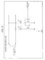
- Fig. 3 is a diagram illustrating a configuration of a transmitting circuit 155A including a resistor and a MOS switch. As illustrated in Fig. 3 , the transmitting circuit 155A is configured such that a resistor 175 is connected with a MOS transistor 177 in series, and a resistor 176 is connected with a MOS transistor 178 in series.
- R11 indicates a resistance value of the resistor 175, and R12 indicates a resistance value of the resistor 176.
- One terminal of the resistor 175 is connected to one terminal (the upper terminal in Fig. 3 ) of the coil 131 of the antenna circuit 111, and the other terminal thereof is connected to a drain terminal of the MOS transistor 177.
- the drain terminal of the MOS transistor 177 is connected to the other terminal of the resistor 175, and a source terminal thereof is grounded. Further, a signal indicating "1" or "0" according to the transmission data received from the communication control unit 172, that is, the modulated signal is supplied to the gate terminal of the MOS transistor 177.
- the MOS transistor 177 performs an ON/OFF switching operation according to the modulated signal of "1" or "0".
- one terminal of the resistor 176 is connected to the other terminal (the lower terminal in Fig. 3 ) of the coil 131 of the antenna circuit 111, and the other terminal thereof is connected to a drain terminal of the MOS transistor 178.
- the drain terminal of the MOS transistor 178 is connected to the other terminal of the resistor 176, and a source terminal thereof is grounded.
- the modulated signal from the communication control unit 172 is supplied to the gate terminal of the MOS transistor 178.
- the MOS transistor 178 performs the ON/OFF switching operation according to the modulated signal of "1" or "0".
- the impedance of the parallel resonant circuit of the antenna circuit 111 is changed.
- the carrier generated in the antenna circuit 111 is changed, and the load modulation is performed.
- Fig. 4 is a diagram illustrating a configuration of a transmitting circuit 155B including a capacitor and a MOS switch. As illustrated in Fig. 4 , the transmitting circuit 155B is configured such that a capacitor 179 is connected with a MOS transistor 177 in series, and a capacitor 180 is connected with a MOS transistor 178 in series.
- C12 indicates a capacitance of the capacitor 179
- C13 indicates a capacitance of the capacitor 180.
- the MOS transistor 177 has basically the same connection relation as in Fig. 3 , but one terminal of the capacitor 179 is connected to a drain terminal of the MOS transistor 177. Further, the other terminal of the capacitor 179 is connected to one terminal (the upper terminal in Fig. 4 ) of the coil 131 of the antenna circuit 111. Similarly, the MOS transistor 178 has basically the same connection relation as in Fig. 3 , but one terminal of the capacitor 180 is connected to a drain terminal of the MOS transistor 178. The other terminal of the capacitor 180 is connected to the other terminal (the lower terminal in Fig. 4 ) of the coil 131 of the antenna circuit 111.
- the MOS transistors 177 and 178 perform the switching operation according to the modulated signal, the load modulation of changing the impedance of the parallel resonant circuit of the antenna circuit 111 is performed.
- Fig. 5 is a diagram illustrating a configuration of a transmitting circuit 155C including a diode and a MOS switch. As illustrated in Fig. 5 , the transmitting circuit 155C is configured such that a diode 181 is connected with a MOS transistor 177 in series, and a diode 182 is connected with a MOS transistor 178 in series.
- the MOS transistor 177 has basically the same connection relation as in Fig. 3 , but a cathode side of the diode 181 is connected to a drain terminal of the MOS transistor 177. An anode side of the diode 181 is connected to one terminal (the upper terminal in Fig. 5 ) of the coil 131 of the antenna circuit 111.
- the MOS transistor 178 has basically the same connection relation as in Fig. 3 , but a cathode side of the diode 182 is connected to a drain terminal of the MOS transistor 178. An anode side of the diode 182 is connected to the other terminal (the lower terminal in Fig. 5 ) of the coil 131 of the antenna circuit 111.
- the MOS transistors 177 and 178 perform the switching operation according to the modulated signal, the load modulation of changing the impedance of the parallel resonant circuit of the antenna circuit 111 is performed.
- Fig. 6 is a diagram illustrating a configuration of a transmitting circuit 155D including a combination of a diode and a resistor and a MOS switch. As illustrated in Fig. 6 , the transmitting circuit 155D is configured such that a diode 181, a resistor 175, and a MOS transistor 177 are connected in series, and a diode 182, a resistor 176, and a MOS transistor 178 are connected in series.
- the resistor 175 and the MOS transistor 177 have basically the same connection relation as in Fig. 3 , but a cathode side of the diode 181 is connected to one terminal of the resistor 175. An anode side of the diode 181 is connected to one terminal (the upper terminal in Fig. 6 ) of the coil 131 of the antenna circuit 111.
- the resistor 176 and the MOS transistor 178 have basically the same connection relation as in Fig. 3 , but a cathode side of the diode 182 is connected to one terminal of the resistor 176. An anode side of the diode 182 is connected to the other terminal (the lower terminal in Fig. 6 ) of the coil 131 of the antenna circuit 111.
- the MOS transistors 177 and 178 perform the switching operation according to the modulated signal, the load modulation of changing the impedance of the parallel resonant circuit of the antenna circuit 111 is performed.
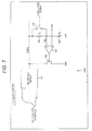
- Fig. 7 is a diagram illustrating a configuration of a transmitting circuit 155E that controls load modulation using feedback control.
- the transmitting circuit 155E includes a rectifying circuit 183, a resistor 184, a resistor 185, a switch 186, an operational amplifier 187, and a MOS transistor 188.
- R 1 indicates a resistance value of the resistor 184
- R 2 indicates a resistance value of the resistor 185.
- One terminal of the resistor 184 is connected to an output terminal of the rectifying circuit 183, and the other terminal thereof is connected to one terminal of the resistor 185.
- the switch 186 is connected to both ends of the resistor 184.
- the other terminal of the resistor 185 is grounded.
- One input terminal (a + terminal) of the operational amplifier 187 is connected between the resistor 184 and the resistor 185, and the other input terminal (a - terminal) is connected to a reference voltage circuit (not illustrated).
- An output terminal of the operational amplifier 187 is connected to a gate terminal of the MOS transistor 188 for voltage control.
- a drain terminal of the MOS transistor 188 is connected to an output terminal of the rectifying circuit 183, and a source terminal thereof is grounded.
- a gate terminal of the MOS transistor 188 is connected to an output terminal of the operational amplifier 187.
- a signal (Vin) rectified by the rectifying circuit 183 and then divided by the resistor 184 and the resistor 185 is input to one input terminal (the + terminal) of the operational amplifier 187, and a certain reference voltage (Vref) is input to the other input terminal (the - terminal) of the operational amplifier 187 from the reference voltage circuit.
- the modulated signal is used as a control signal for controlling an ON/OFF operation of the switch 186.
- the transmitting circuit 155E it is possible to obtains an amplitude difference of R 1 /R 2 *Vref on the signal of VDDA by turning the switch 186 on or off by the modulated signal. Further, the amplitude difference is shown as an impedance variation in the antenna coil terminal via the rectifying circuit 183.
- Fig. 7 has been described in connection with the example in which the resistor 184 is short-circuited, but the impedance can be changed such that the resistance value R 1 of the resistor 184 is divided into several values and switching some resistors to any one of the effective state and the short-circuited state.
- the rectifying circuit 183 and the rectifying circuit 157 of Fig. 2 may be implemented as a single circuit.
- circuit configurations of Figs. 3 to 7 are examples, and it is possible to employ another circuit configuration capable of performing load modulation.
- the transmitting circuit 155 has the above-described configuration.
- a communication device 101-1 and a communication device 101-2 are arranged at positions at which Near Field communication can be performed, the communication device 101-1 is assumed to operate in the reader/writer mode, and the communication device 101-2 is assumed to operate in the tag mode. Further, detailed internal configurations of an integrated circuit 112-1, an external circuit 115-1, an integrated circuit 112-2, and an external circuit 115-2 are omitted, but the circuits have the configurations illustrated in Fig. 2 , and thus "-1" is added to reference numerals of internal circuits of the former, and "-2" is added to reference numerals of internal circuits of the latter.
- the control signal (MODE) is supplied from the host controller 113-1 to the mode control unit 171-1 of the integrated circuit 112-1.
- the mode control unit 171-1 performs control according to the control signal (MODE) given from the host controller 113-1 such that the respective units of the integrated circuit 112-1 such as the transmitting circuit 155-1 and the receiving circuit 158-1 operate in the reader/writer mode.
- the host controller 113-1 checks whether or not another reader/writer around the communication device 101-1 is generating a magnetic field, and supplies the control signal (MODE) indicating transition to the reader/writer mode to the mode control unit 171-1 when another reader/writer is generating no magnetic field.
- the control signal (EN) is supplied from the host controller 113-1 to the external circuit 115-1.
- the switch 193-1 enters the ON state according to the control signal (EN) given from the host controller 113-1.
- electric power is supplied from the power source 114-1 to the oscillating circuit 191-1, and the oscillating circuit 191-1 starts to generate the oscillation signal.
- the tri-state inverter circuit 194-1 and the tri-state buffer circuit 197-1 cause their output states to transition from the high impedance output state to the normal output state according to the control signal (EN) given from the host controller 113-1.
- the tri-state inverter circuit 194-1 inverts the oscillation signal received from the oscillating circuit 191-1, and supplies the inverted oscillation signal to the filter circuit 195-1.
- the filter circuit 195-1 generates the carrier of 13.56 MHz based on the oscillation signal from the tri-state inverter circuit 194-1.
- the tri-state buffer circuit 197-1 supplies the oscillation signal received from the oscillating circuit 191-1 to the filter circuit 198-1.
- the filter circuit 198-1 generates the carrier of 13.56 MHz based on the oscillation signal from the tri-state buffer circuit 197-1.
- the carrier of 13.56 MHz based on the outputs of the filter circuit 195-1 and the filter circuit 198-1 is generated in the antenna circuit 111-1.
- the impedance of the parallel resonant circuit of the antenna circuit 111 has a value of a predetermined magnitude through the impedance circuit 196-1 and the impedance circuit 199-1.
- the carrier of 13.56 MHz is generated in the antenna circuit 111-1 by the external circuit 115-1.
- the host controller 113-1 supplies transmission data that is transmitted to the communication device 101-2 of the communication destination to the data input circuit 153-1.
- the communication control unit 172-1 encodes the transmission data input from the host controller 113-1 according to the Manchester scheme.
- the transmitting circuit 155-1 performs the load modulation on the carrier generated in the antenna circuit 111-1 by the external circuit 115-1 by changing the impedance of the parallel resonant circuit of the antenna circuit 111-1 according to the Manchester-encoded transmission data received from the communication control unit 172-1.
- the modulated signal is transmitted from the communication device 101-1 to the communication device 101-2 of the communication destination through the carrier.
- the communication device 101-2 converts the AC voltage obtained from the carrier generated in the antenna circuit 111-1 of the communication device 101-1 into the DC voltage, starts its operation, and transmits reply data by performing the load modulation in a state in which the modulated signal is received from the communication device 101-1.
- the modulated signal generated by the load modulation performed by the communication device 101-2 of the communication destination is induced in the antenna circuit 111-1 of the communication device 101-1.
- the receiving circuit 158-1 demodulates the modulated signal based on the output from the rectifying circuit 157-1.
- the communication control unit 172-1 decodes the Manchester encoded reception data received from the receiving circuit 158-1, and supplies the decoded reception data to the host controller 113-1 through the data output circuit 154-1.
- the communication device 101-1 operating in the reader/writer mode has been described above.
- the communication device 101-2 When the communication device 101-2 approaches the communication device 101-1 operating in the reader/writer mode, the carrier radiated from the antenna circuit 111-1 of the communication device 101-1 is received by the antenna circuit 111-2. At this time, the received AC voltage generated in the antenna circuit 111-2 is converted into the DC voltage through the rectifying circuit 157-2, and the communication device 101-2 acquires a power voltage necessary for its operation and starts its operation.
- the power voltage may be supplied from the power source 114-2, and the power voltage may be selected by the power selecting circuit 159-2.
- the control signal (MODE) is supplied from the host controller 113-2 to the mode control unit 171-2.
- the mode control unit 171-2 performs control according to the control signal (MODE) given from the host controller 113-2 such that the respective units of the integrated circuit 112-2 such as the transmitting circuit 155-2 and the receiving circuit 158-2 operate in the tag mode.
- the control signal (EN) is supplied from the host controller 113-2 to the external circuit 115-2.
- the switch 193-2 enters the OFF state according to the control signal (EN) given from the host controller 113-2. As a result, electric power from the power source 114-2 is not supplied to the oscillating circuit 191-2, and the generation of the oscillation signal is stopped.
- the tri-state inverter circuit 194-2 and the tri-state buffer circuit 197-2 cause the output state to transition to the high impedance output state according to the control signal (EN) given from the host controller 113-2. As a result, the outputs of the tri-state inverter circuit 194-2 and the tri-state buffer circuit 197-2 become the high impedance state.
- the receiving circuit 158-2 demodulates the modulated signal based on the output from the rectifying circuit 157-2.
- the communication control unit 172-2 decodes the Manchester-encoded reception data received from the receiving circuit 158-2, and supplies the decoded reception data to the host controller 113-2 through the data output circuit 154-2.
- the host controller 113-2 supplies transmission data to be replied to the communication device 101-1 of the communication destination to the data input circuit 153-2 in response to the reception data received from the data output circuit 154-2.
- the communication control unit 172-2 encodes the transmission data input from the host controller 113-2 according to the Manchester scheme.
- the transmitting circuit 155-2 performs the load modulation on the Manchester-encoded transmission data received from the communication control unit 172-2 by changing the impedance of the parallel resonant circuit of the antenna circuit 111-2, and transmits the resultant transmission data to the communication device 101-1 of the communication destination.
- the modulated signal is transmitted from the communication device 101-2 to the communication device 101-1 of the communication destination through the load modulation.
- the communication device 101-2 operating in the tag mode has been described above.
- the integrated circuit 112 transmits the transmission data to the communication destination by performing the load modulation of changing the impedance of the parallel resonant circuit of the antenna circuit 111 according to the transmission data using the carrier generated in the antenna circuit 111 by the external circuit 115. Further, when the operation is performed in the tag mode, the integrated circuit 112 receives data transmitted from the communication destination, and transmits transmission data to be transmitted in response to the reception data to the communication destination using the load modulation.
- the integrated circuit 112 modulates the transmission data using the same load modulation scheme as the time of transmission in the tag mode without using the ASK modulation scheme, and thus it is unnecessary to install a plurality of transmitting circuits according to the modulation schemes, and the transmitting circuit is commonalized.
- the transmitting circuit 155 is provided as a transmitting circuit dedicated for a load modulation scheme. This can be implemented using the fact that the same coding scheme (for example, the Manchester scheme) is used at the time of transmission and reception according a predetermined standard (for example, FeliCa (a registered trademark)). Further, in the configuration of Fig. 2 , since the same coding scheme (for example, the Manchester scheme) is used at the time of transmission and reception according as a predetermined standard, an encoding circuit (not illustrated) of the communication control unit 172 is also commonalized.
- the transmitting circuit 155 is commonalized in the reader/writer mode and the tag mode, and the manufacturing cost is reduced, and it is consequently possible to provide the communication device 101 at a low price. Further, when attention is given to the integrated circuit 112, the transmitting circuit 155 can be commonalized, and the external circuit 115 that generates the carrier can be mounted as a separate circuit, and thus it is possible to provide the integrated circuit 112 at a low price and reduce a circuit size.
- the communication device 101-1 operates in the reader/writer mode, and the communication device 101-2 operates in the tag mode, but conversely, the communication device 101-1 may operate in the tag mode, and the communication device 101-2 may operate in the reader/writer mode.
- the communication device 101 has been described as the communication destination, but an external device having only one of functions of the RF tag and the reader/writer may be the communication destination.
- an RF tag or a non-contact type IC card has a configuration in which a voltage does not increase to be a predetermined set voltage or higher due to a withstand voltage of an integrated circuit (chip) or a relation with a communication performance or the like.
- a waveform of a carrier is likely to be distorted.
- a radio frequency component is likely to be problematic due to distortion (for example, a sine wave gets close to a square wave) of a waveform of a carrier.
- distortion for example, a sine wave gets close to a square wave
- carrier distortion since the carrier is transmitted, it is necessary to maintain a waveform of a sine wave, but in the case of the tag mode, it is unnecessary to maintain a waveform of a sine wave, and thus carrier distortion is not problematic.
- a voltage setting circuit 160 may be additionally provided and set a voltage value according to an operation mode.
- the voltage setting circuit 160 includes a step-down element (for example, a resistor element, a diode element, or the like), a switch of turning on or off the step-down element according to an operation state, and a shunt regulator circuit, and is installed behind the rectifying circuit 157.
- the voltage setting circuit 160 performs control according to control of the mode control unit 171 such that a voltage value of the DC voltage converted by the rectifying circuit 157 does not increase to be a set voltage or higher.
- the voltage setting circuit 160 sets a voltage between the antenna coil terminals to a set voltage of 8 V by validating the step-down element by the control signal (MODE) and increasing a set voltage of the shunt regulator circuit.
- the voltage setting circuit 160 sets the voltage between the antenna coil terminals to a set voltage of 4 V by invalidating the step-down element by the control signal (MODE) and decreasing the set voltage of the shunt regulator circuit.
- the integrated circuit 112 when the operation is performed in the reader/writer mode, even when a high voltage is set for a high output, the waveform of the sine wave of the carrier is maintained.
- the integrated circuit 112 when the operation is performed in the tag mode, since a low set voltage is set, for example, it is possible to reliably prevent an integrated circuit (chip) from being broken.
- the voltage setting circuit 160 may fixedly set the set voltage for the tag mode as the set voltage regardless of the operation mode as long as the set voltage for the tag mode does not cause any problem in the waveform of the sine wave of the carrier.
- Fig. 10 is a diagram illustrating a configuration of a communication system according to an embodiment of the present technology.
- a communication system 201 includes a communication device 102, a carrier generating device 211, and an RF tag 212.
- the communication device 102 operates in the reader/writer mode, and performs Near Field communication with the RF tag 212 of the communication destination.
- the communication device 102 includes an antenna circuit 111, an integrated circuit 112, a host controller 113, and a power source 114.
- the antenna circuit 111, the integrated circuit 112, the host controller 113, and the power source 114 have configurations similar to the antenna circuit 111, the integrated circuit 112, the host controller 113, and the power source 114 of Fig. 2 .
- the communication device 102 has a configuration in which the external circuit 115 generating the carrier is removed from the communication device 101 of Fig. 2 .
- the carrier generating device 211 that generates the carrier is installed instead of the external circuit 115.
- the carrier generating device 211 includes an oscillating circuit 251, a crystal oscillator 252, a power source 253, a switch 254, a coil 255, and a capacitor 256.
- the oscillating circuit 251 generates an oscillation signal corresponding to a vibration frequency of the crystal oscillator 252.
- the power source 253 supplies the power voltage to the oscillating circuit 251.
- the switch 254 performs the ON/OFF switching operation according to control of a higher host controller (not illustrated).
- the coil 255 and the capacitor 256 form a parallel resonant circuit.
- L12 indicates inductance of the coil 255
- C14 indicates capacitance of the capacitor.
- the carrier generating device 211 when the switch 254 transitions from the OFF state to the ON state, the power voltage is supplied from the power source 253 to the oscillating circuit 251.
- the oscillating circuit 251 starts its operation according to the power voltage supplied from the power source 253, and generates the oscillation signal corresponding to the vibration frequency of the crystal oscillator 252.
- the oscillation signal is applied to the parallel resonant circuit configured with the coil 255 and the capacitor 256, and a magnetic field is generated.
- a carrier (carrier wave) of a predetermined frequency 13.56 MHz
- the transmitting circuit 155 of the communication device 102 When the operation is performed in the reader/writer mode, if it enters a communicable state with the RF tag 212 of the communication destination, the transmitting circuit 155 of the communication device 102 performs the load modulation on the carrier generated in the antenna circuit 111 by the carrier generating device 211 by changing the impedance of the parallel resonant circuit of the antenna circuit 111 according to the transmission data received from the communication control unit 172. As a result, the modulated signal is transmitted from the communication device 102 to the RF tag 212 of the communication destination.
- the RF tag 212 converts the AC voltage obtained from the carrier generated in the antenna circuit 111 of the communication device 102 into the DC voltage, starts its operation, and transmits reply data by performing the load modulation in a state in which the modulated signal is received from the communication device 102.
- the modulated signal generated by the load modulation performed by the RF tag 212 of the communication destination is induced in the antenna circuit 111 of the communication device 102.
- the receiving circuit 158 demodulates the modulated signal generated in the antenna circuit 111 based on the output from the rectifying circuit 157, and supplies reception data obtained by the demodulating to the communication control unit 172.
- the communication device 102 does not include the external circuit 115, and transmits the transmission data to the RF tag 212 of the communication destination by performing the load modulation on the carrier in the antenna circuit 111 by the carrier generating device 211.
- the transmission data is modulated using the same load modulation scheme at the time of transmission in the reader/writer mode and the tag mode, and thus data can be transmitted and received using the carrier generated by the carrier generating device 211.
- the communication system 201 has the above-described configuration.
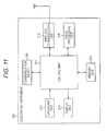
- Fig. 11 is a diagram illustrating a configuration of an electronic instrument according to an embodiment of the present technology.
- an electronic instrument 301 is a portable information device or a portable communication device such as a mobile telephone, a smart phone, or a tablet PC. As illustrated in Fig. 11 , the electronic instrument 301 includes a communication device 101, a control unit 311, a memory unit 312, an operating unit 313, a display unit 314, a wireless communication unit 315, and a voice processing unit 316.
- the control unit 311 controls the respective units of the electronic instrument 301.
- the memory unit 312 holds various kinds of data according to control of the control unit 311.
- the control unit 311 has the function of the host controller 113 (for example, Fig. 2 ) described above, and controls the operation mode of the communication device 101.
- the communication device 101 operates in the reader/writer mode or the tag mode according to control of the control unit 311.
- the communication device 101 transmits transmission data to an RF tag of a communication destination (not illustrated) using the load modulation scheme according to control of the control unit 311. Further, the communication device 101 receives reply data transmitted from the RF tag of the communication destination according to control of the control unit 311.
- the communication device 101 receives data transmitted from a reader/writer of a communication destination (not illustrated) according to control of the control unit 311. Furthermore, the communication device 101 transmits reply transmission data to the reader/writer of the communication destination using the load modulation scheme according to control of the control unit 311.
- the operating unit 313 supplies an operation signal according to a user's operation to the control unit 311.
- the control unit 311 controls the operations of the respective units of the electronic instrument 301 according to the operation signal given from the operating unit 313.
- the operating unit 313 may be a physical button and may be a Graphical User Interface (GUI) image displayed on a screen of the display unit 314 having a touch panel.
- GUI Graphical User Interface
- the display unit 314 is configured with a display device such as a Liquid Crystal Display (LCD).
- the display unit 314 displays various kinds of information such as a text or an image according to control of the control unit 311.
- the wireless communication unit 315 performs wireless communication with a predetermined server via a network such as the Internet according to control of the control unit 311.
- the voice processing unit 316 includes a device for performing a voice call such as a microphone or a speaker.
- the voice processing unit 316 performs a voice input process or a voice output process according to control of the control unit 311.
- the electronic instrument 301 has the above-described configuration.
- the communication device 101 since the communication device 101 is mounted in the electronic instrument 301, for example, when another electronic instrument having an RF tag function is held over the electronic instrument 301, the communication device 101 operates in the reader/writer mode, and performs transmission and reception of data with another electronic instrument. For example, when the electronic instrument 301 is held over a reader/writer equipped in a ticket gate of a station or a cache register of a store, the communication device 101 operates in the tag mode, and performs transmission and reception of data with the reader/writer.
- the transmitting circuit 155 is commonalized in the reader/writer mode and the tag mode, and the manufacturing cost is lowered, and thus it is possible to provide the communication device 101 ( Fig. 2 ), the communication device 102 ( Fig. 10 ), or the electronic instrument 301 ( Fig. 11 ) at a low price.
- the transmitting circuit 57 for the reader/writer mode and the transmitting circuit 61 for the tag mode separately as illustrated in Fig. 1 , it is necessary to commonalize the transmitting circuits dedicated for the modes and reduce the manufacturing cost, but this demand can be satisfied by the present technology.
- the integrated circuit 112 for example, Fig. 2
- the circuit for generating the carrier such as the oscillating circuit 15 or the crystal oscillator 16 is necessary as illustrated in Fig. 1 , but in the present technology, since a separate circuit can be mounted as the external circuit 115, it is possible to provide the integrated circuit 112 at a low price and reduce the circuit size.
- the communication device 102 ( Fig. 10 ) can perform transmission and reception of data using the carrier generated by the carrier generating device 211 instead of the external circuit 115 without including the external circuit 115 serving as a separate circuit from the integrated circuit 112.
- the carrier generated by the carrier generating device 211 instead of the external circuit 115 without including the external circuit 115 serving as a separate circuit from the integrated circuit 112.
- the external circuit 115 is not mounted in the communication device 102, power consumption can be reduced.
- the communication system can be constructed without using the carrier generating device 211 such that the integrated circuit 112 and the external circuit 115 are mounted on the same substrate, and Near Field communication can be performed among all electronic instruments equipped with a module in which the integrated circuit 112 and the external circuit 115 are mounted.
- the integrated circuit 12 ( Fig. 1 ) of the related art, when the operation is performed in the reader/writer mode, the ASK modulation of driving the carrier at a low impedance and modulating an amplitude compulsorily is used, and thus it is necessary to change a level thereof compulsorily while driving the carrier at the low impedance.
- the transmitting buffer circuits 58 and 59 are installed behind the transmitting circuit 57.
- the load modulation scheme is used, and in the load modulation scheme, an impedance (for example, about several hundreds to 1 K ⁇ ) of a certain magnitude is applied, and the modulation is performed according to an amount of change in an impedance, and thus the transmitting buffer circuits 58 and 59 are unnecessary in the integrated circuit 112 (for example, Fig. 2 ).
- the transmitting buffer circuits 58 and 59 are unnecessary in the integrated circuit 112 (for example, Fig. 2 ).
- the size and the cost can be reduced.
- a communication target when the communication device 101, the communication device 102, or the electronic instrument 301 operates in the reader/writer mode is an RF tag
- the present technology is not limited to this example, and, for example, communication devices performing Near Field communication with an RFID reader/writer according to an electromagnetic coupling scheme such as a non-contact type IC card can serve as a communication target.
- the present technology may have the following configurations.
- a communication device including:
- the communication device further including:
- the communication device wherein the carrier generating unit causes the impedance of the antenna unit to have a value of a predetermined magnitude.
- the communication device wherein the first carrier is generated by an external carrier generating device.
- the communication device according to any one of (1) to (4), wherein the transmission data and the reception data are encoded by the same coding scheme.
- the communication device according to any one of (1) to (5), further including:
- a communication method of a communication device including:
- An integrated circuit including:
- a communication method of an integrated circuit including:
- An electronic instrument equipped with a communication device including:
Landscapes
- Engineering & Computer Science (AREA)
- Physics & Mathematics (AREA)
- Health & Medical Sciences (AREA)
- Toxicology (AREA)
- Computer Networks & Wireless Communication (AREA)
- Electromagnetism (AREA)
- General Health & Medical Sciences (AREA)
- Artificial Intelligence (AREA)
- Computer Vision & Pattern Recognition (AREA)
- General Physics & Mathematics (AREA)
- Theoretical Computer Science (AREA)
- Signal Processing (AREA)
- Computer Security & Cryptography (AREA)
- Near-Field Transmission Systems (AREA)
- Power Engineering (AREA)
Applications Claiming Priority (2)
| Application Number | Priority Date | Filing Date | Title |
|---|---|---|---|
| JP2012271030 | 2012-12-12 | ||
| PCT/JP2013/082014 WO2014091934A1 (ja) | 2012-12-12 | 2013-11-28 | 通信装置、通信方法、集積回路、及び、電子機器 |
Publications (3)
| Publication Number | Publication Date |
|---|---|
| EP2933757A1 true EP2933757A1 (de) | 2015-10-21 |
| EP2933757A4 EP2933757A4 (de) | 2016-07-13 |
| EP2933757B1 EP2933757B1 (de) | 2019-05-01 |
Family
ID=50934227
Family Applications (1)
| Application Number | Title | Priority Date | Filing Date |
|---|---|---|---|
| EP13863384.7A Not-in-force EP2933757B1 (de) | 2012-12-12 | 2013-11-28 | Kommunikationsvorrichtung, kommunikationsverfahren, integrierte schaltung und elektronisches instrument |
Country Status (6)
| Country | Link |
|---|---|
| US (1) | US9904820B2 (de) |
| EP (1) | EP2933757B1 (de) |
| JP (1) | JP6249238B2 (de) |
| KR (1) | KR102096681B1 (de) |
| CN (1) | CN104823204B (de) |
| WO (1) | WO2014091934A1 (de) |
Families Citing this family (13)
| Publication number | Priority date | Publication date | Assignee | Title |
|---|---|---|---|---|
| JP2666555B2 (ja) | 1990-10-02 | 1997-10-22 | 石川島播磨重工業株式会社 | 船の二重殻構造物及びその構築方法 |
| US20120203620A1 (en) | 2010-11-08 | 2012-08-09 | Douglas Howard Dobyns | Techniques For Wireless Communication Of Proximity Based Marketing |
| US8929809B2 (en) | 2011-03-22 | 2015-01-06 | Radeum, Inc. | Techniques for wireless communication of proximity based content |
| US8880100B2 (en) | 2011-03-23 | 2014-11-04 | Radium, Inc. | Proximity based social networking |
| JP6128986B2 (ja) * | 2013-06-24 | 2017-05-17 | 任天堂株式会社 | 通信システム、通信端末装置、通信プログラム、および通信方法 |
| US9705564B2 (en) | 2014-08-29 | 2017-07-11 | Freelinc Technologies | Spatially enabled secure communications |
| US10164685B2 (en) | 2014-12-31 | 2018-12-25 | Freelinc Technologies Inc. | Spatially aware wireless network |
| CN107094037B (zh) * | 2017-03-24 | 2019-10-25 | 深圳市文鼎创数据科技有限公司 | 动态令牌的前端硬件电路及其授种子或生产配置的方法 |
| CN106909865B (zh) * | 2017-03-24 | 2019-10-25 | 深圳市文鼎创数据科技有限公司 | 近场通信前端硬件电路、终端、读写器、系统以及方法 |
| CN109426164B (zh) * | 2017-08-25 | 2021-06-08 | 上海芯龙半导体技术股份有限公司 | 一种用于中央空调系统中信号传输的载波集成电路 |
| JP7115723B2 (ja) * | 2018-01-04 | 2022-08-09 | ラピスセミコンダクタ株式会社 | 半導体装置および半導体モジュール |
| WO2020241670A1 (ja) * | 2019-05-28 | 2020-12-03 | ラピスセミコンダクタ株式会社 | 通知応答回路 |
| US20220092280A1 (en) * | 2019-12-31 | 2022-03-24 | Queclink Wireless Solutions Co., Ltd. | Rfid tag information reading apparatus and method |
Family Cites Families (13)
| Publication number | Priority date | Publication date | Assignee | Title |
|---|---|---|---|---|
| JP4501241B2 (ja) | 2000-07-10 | 2010-07-14 | ソニー株式会社 | Icカード及びicカードのデータ通信方法 |
| CA2533029C (en) * | 2003-07-22 | 2014-06-03 | Nokia Corporation | Reader device for radio frequency identification transponder with transponder functionality |
| JP2006067448A (ja) | 2004-08-30 | 2006-03-09 | Ricoh Co Ltd | 通信装置およびこの通信装置を備えた携帯電子機器 |
| JP4797991B2 (ja) | 2005-04-15 | 2011-10-19 | ソニー株式会社 | 通信装置、それを搭載した非接触型icカード、および情報機器 |
| US7729660B2 (en) | 2005-04-15 | 2010-06-01 | Sony Corporation | Communication device, non-contact type IC card mounting same, and information apparatus |
| US8269630B2 (en) * | 2005-12-09 | 2012-09-18 | Tego Inc. | Methods and systems of a multiple radio frequency network node RFID tag |
| JP2007219585A (ja) * | 2006-02-14 | 2007-08-30 | Seiko Epson Corp | 非接触通信方式および非接触通信システム |
| JP4525715B2 (ja) * | 2007-08-20 | 2010-08-18 | ソニー株式会社 | 通信装置、通信方法、および通信システム |
| JP4645698B2 (ja) | 2008-08-19 | 2011-03-09 | ソニー株式会社 | 無線通信装置と受電装置 |
| JP4748211B2 (ja) * | 2008-12-02 | 2011-08-17 | ソニー株式会社 | 通信装置、並びに適応等化装置 |
| JP2011060086A (ja) * | 2009-09-11 | 2011-03-24 | Ricoh Co Ltd | Rfidタグ、リーダ・ライタ及びrfidシステム |
| JP2011215865A (ja) * | 2010-03-31 | 2011-10-27 | Sony Corp | 信号処理装置及び信号処理方法 |
| US9397726B2 (en) * | 2010-08-23 | 2016-07-19 | Radeum, Inc. | System and method for communicating between near field communication devices within a target region using near field communication |
-
2013
- 2013-11-28 CN CN201380063335.1A patent/CN104823204B/zh not_active Expired - Fee Related
- 2013-11-28 WO PCT/JP2013/082014 patent/WO2014091934A1/ja not_active Ceased
- 2013-11-28 US US14/441,321 patent/US9904820B2/en active Active
- 2013-11-28 EP EP13863384.7A patent/EP2933757B1/de not_active Not-in-force
- 2013-11-28 KR KR1020157014538A patent/KR102096681B1/ko not_active Expired - Fee Related
- 2013-11-28 JP JP2014551967A patent/JP6249238B2/ja active Active
Also Published As
| Publication number | Publication date |
|---|---|
| KR102096681B1 (ko) | 2020-04-02 |
| HK1211118A1 (en) | 2016-05-13 |
| CN104823204B (zh) | 2018-08-21 |
| CN104823204A (zh) | 2015-08-05 |
| WO2014091934A1 (ja) | 2014-06-19 |
| US20150254481A1 (en) | 2015-09-10 |
| EP2933757B1 (de) | 2019-05-01 |
| KR20150094614A (ko) | 2015-08-19 |
| EP2933757A4 (de) | 2016-07-13 |
| JPWO2014091934A1 (ja) | 2017-01-05 |
| US9904820B2 (en) | 2018-02-27 |
| JP6249238B2 (ja) | 2017-12-20 |
Similar Documents
| Publication | Publication Date | Title |
|---|---|---|
| EP2933757B1 (de) | Kommunikationsvorrichtung, kommunikationsverfahren, integrierte schaltung und elektronisches instrument | |
| US8583075B2 (en) | Power supply control apparatus and method thereof and mobile apparatus using the same | |
| US9367713B2 (en) | Contactless communication device | |
| US8099045B2 (en) | Near field communication system and associated apparatus | |
| US8897699B2 (en) | Reducing emissions in a near field communications (NFC) capable device | |
| JP5177270B2 (ja) | 通信装置、通信システム、および通信方法 | |
| CN1920847B (zh) | 具有撷取电源电压的装置的电感耦合读取器 | |
| JP4618672B2 (ja) | 半導体集積回路および無線通信装置 | |
| KR20140110389A (ko) | 비접촉 통신 장치 및 그것을 포함한 유저 장치 | |
| US9041515B2 (en) | Apparatus comprising display driving integrated circuit and radio-frequency identification reader | |
| CN109787658B (zh) | 一种nfc线圈驱动装置、方法及电子设备 | |
| KR200398970Y1 (ko) | 상이한 주파수대역을 갖는 이종의 태그가 탑재된 알에프카드 | |
| HK1211118B (en) | Communication device, communication method, integrated circuit, and electronic instrument | |
| CN203882331U (zh) | 一种无线感应供电带显示屏的储值卡 | |
| EP4524811A1 (de) | Hf-kommunikationsvorrichtung zur adaptiven detektion weiterer hf-kommunikationsvorrichtungen | |
| KR200299286Y1 (ko) | 패시브 타입 비접촉식 아이씨카드를 액티브 타입비접촉식 아이씨카드로 활용하는 장치 | |
| CN104318295A (zh) | 具有拨号通话功能的双频复用天线rfid标签 | |
| CN204155304U (zh) | 具有拨号通话功能的双频复用天线rfid标签 | |
| CN105490709B (zh) | 一种小型无源射频放大装置及其实现方法 | |
| CN104299027A (zh) | 可实现电话机通话的双频复用天线rfid标签 | |
| HK1193246A (en) | A near field communication (nfc) device and an antenna module thereof | |
| JP2013171512A (ja) | Rfid搭載携帯端末 |
Legal Events
| Date | Code | Title | Description |
|---|---|---|---|
| PUAI | Public reference made under article 153(3) epc to a published international application that has entered the european phase |
Free format text: ORIGINAL CODE: 0009012 |
|
| 17P | Request for examination filed |
Effective date: 20150605 |
|
| AK | Designated contracting states |
Kind code of ref document: A1 Designated state(s): AL AT BE BG CH CY CZ DE DK EE ES FI FR GB GR HR HU IE IS IT LI LT LU LV MC MK MT NL NO PL PT RO RS SE SI SK SM TR |
|
| AX | Request for extension of the european patent |
Extension state: BA ME |
|
| DAX | Request for extension of the european patent (deleted) | ||
| REG | Reference to a national code |
Ref country code: DE Ref legal event code: R079 Ref document number: 602013054815 Country of ref document: DE Free format text: PREVIOUS MAIN CLASS: G06K0017000000 Ipc: H04B0005000000 |
|
| A4 | Supplementary search report drawn up and despatched |
Effective date: 20160610 |
|
| RIC1 | Information provided on ipc code assigned before grant |
Ipc: H04B 5/00 20060101AFI20160606BHEP |
|
| GRAP | Despatch of communication of intention to grant a patent |
Free format text: ORIGINAL CODE: EPIDOSNIGR1 |
|
| STAA | Information on the status of an ep patent application or granted ep patent |
Free format text: STATUS: GRANT OF PATENT IS INTENDED |
|
| INTG | Intention to grant announced |
Effective date: 20181126 |
|
| GRAS | Grant fee paid |
Free format text: ORIGINAL CODE: EPIDOSNIGR3 |
|
| GRAA | (expected) grant |
Free format text: ORIGINAL CODE: 0009210 |
|
| STAA | Information on the status of an ep patent application or granted ep patent |
Free format text: STATUS: THE PATENT HAS BEEN GRANTED |
|
| AK | Designated contracting states |
Kind code of ref document: B1 Designated state(s): AL AT BE BG CH CY CZ DE DK EE ES FI FR GB GR HR HU IE IS IT LI LT LU LV MC MK MT NL NO PL PT RO RS SE SI SK SM TR |
|
| REG | Reference to a national code |
Ref country code: GB Ref legal event code: FG4D |
|
| REG | Reference to a national code |
Ref country code: CH Ref legal event code: EP Ref country code: AT Ref legal event code: REF Ref document number: 1128310 Country of ref document: AT Kind code of ref document: T Effective date: 20190515 |
|
| REG | Reference to a national code |
Ref country code: DE Ref legal event code: R096 Ref document number: 602013054815 Country of ref document: DE |
|
| REG | Reference to a national code |
Ref country code: IE Ref legal event code: FG4D |
|
| REG | Reference to a national code |
Ref country code: NL Ref legal event code: MP Effective date: 20190501 |
|
| REG | Reference to a national code |
Ref country code: LT Ref legal event code: MG4D |
|
| PG25 | Lapsed in a contracting state [announced via postgrant information from national office to epo] |
Ref country code: NL Free format text: LAPSE BECAUSE OF FAILURE TO SUBMIT A TRANSLATION OF THE DESCRIPTION OR TO PAY THE FEE WITHIN THE PRESCRIBED TIME-LIMIT Effective date: 20190501 Ref country code: HR Free format text: LAPSE BECAUSE OF FAILURE TO SUBMIT A TRANSLATION OF THE DESCRIPTION OR TO PAY THE FEE WITHIN THE PRESCRIBED TIME-LIMIT Effective date: 20190501 Ref country code: SE Free format text: LAPSE BECAUSE OF FAILURE TO SUBMIT A TRANSLATION OF THE DESCRIPTION OR TO PAY THE FEE WITHIN THE PRESCRIBED TIME-LIMIT Effective date: 20190501 Ref country code: PT Free format text: LAPSE BECAUSE OF FAILURE TO SUBMIT A TRANSLATION OF THE DESCRIPTION OR TO PAY THE FEE WITHIN THE PRESCRIBED TIME-LIMIT Effective date: 20190901 Ref country code: AL Free format text: LAPSE BECAUSE OF FAILURE TO SUBMIT A TRANSLATION OF THE DESCRIPTION OR TO PAY THE FEE WITHIN THE PRESCRIBED TIME-LIMIT Effective date: 20190501 Ref country code: FI Free format text: LAPSE BECAUSE OF FAILURE TO SUBMIT A TRANSLATION OF THE DESCRIPTION OR TO PAY THE FEE WITHIN THE PRESCRIBED TIME-LIMIT Effective date: 20190501 Ref country code: NO Free format text: LAPSE BECAUSE OF FAILURE TO SUBMIT A TRANSLATION OF THE DESCRIPTION OR TO PAY THE FEE WITHIN THE PRESCRIBED TIME-LIMIT Effective date: 20190801 Ref country code: ES Free format text: LAPSE BECAUSE OF FAILURE TO SUBMIT A TRANSLATION OF THE DESCRIPTION OR TO PAY THE FEE WITHIN THE PRESCRIBED TIME-LIMIT Effective date: 20190501 Ref country code: LT Free format text: LAPSE BECAUSE OF FAILURE TO SUBMIT A TRANSLATION OF THE DESCRIPTION OR TO PAY THE FEE WITHIN THE PRESCRIBED TIME-LIMIT Effective date: 20190501 |
|
| PG25 | Lapsed in a contracting state [announced via postgrant information from national office to epo] |
Ref country code: GR Free format text: LAPSE BECAUSE OF FAILURE TO SUBMIT A TRANSLATION OF THE DESCRIPTION OR TO PAY THE FEE WITHIN THE PRESCRIBED TIME-LIMIT Effective date: 20190802 Ref country code: BG Free format text: LAPSE BECAUSE OF FAILURE TO SUBMIT A TRANSLATION OF THE DESCRIPTION OR TO PAY THE FEE WITHIN THE PRESCRIBED TIME-LIMIT Effective date: 20190801 Ref country code: RS Free format text: LAPSE BECAUSE OF FAILURE TO SUBMIT A TRANSLATION OF THE DESCRIPTION OR TO PAY THE FEE WITHIN THE PRESCRIBED TIME-LIMIT Effective date: 20190501 Ref country code: LV Free format text: LAPSE BECAUSE OF FAILURE TO SUBMIT A TRANSLATION OF THE DESCRIPTION OR TO PAY THE FEE WITHIN THE PRESCRIBED TIME-LIMIT Effective date: 20190501 |
|
| REG | Reference to a national code |
Ref country code: AT Ref legal event code: MK05 Ref document number: 1128310 Country of ref document: AT Kind code of ref document: T Effective date: 20190501 |
|
| PG25 | Lapsed in a contracting state [announced via postgrant information from national office to epo] |
Ref country code: IS Free format text: LAPSE BECAUSE OF FAILURE TO SUBMIT A TRANSLATION OF THE DESCRIPTION OR TO PAY THE FEE WITHIN THE PRESCRIBED TIME-LIMIT Effective date: 20190901 |
|
| PG25 | Lapsed in a contracting state [announced via postgrant information from national office to epo] |
Ref country code: EE Free format text: LAPSE BECAUSE OF FAILURE TO SUBMIT A TRANSLATION OF THE DESCRIPTION OR TO PAY THE FEE WITHIN THE PRESCRIBED TIME-LIMIT Effective date: 20190501 Ref country code: DK Free format text: LAPSE BECAUSE OF FAILURE TO SUBMIT A TRANSLATION OF THE DESCRIPTION OR TO PAY THE FEE WITHIN THE PRESCRIBED TIME-LIMIT Effective date: 20190501 Ref country code: RO Free format text: LAPSE BECAUSE OF FAILURE TO SUBMIT A TRANSLATION OF THE DESCRIPTION OR TO PAY THE FEE WITHIN THE PRESCRIBED TIME-LIMIT Effective date: 20190501 Ref country code: AT Free format text: LAPSE BECAUSE OF FAILURE TO SUBMIT A TRANSLATION OF THE DESCRIPTION OR TO PAY THE FEE WITHIN THE PRESCRIBED TIME-LIMIT Effective date: 20190501 Ref country code: CZ Free format text: LAPSE BECAUSE OF FAILURE TO SUBMIT A TRANSLATION OF THE DESCRIPTION OR TO PAY THE FEE WITHIN THE PRESCRIBED TIME-LIMIT Effective date: 20190501 Ref country code: SK Free format text: LAPSE BECAUSE OF FAILURE TO SUBMIT A TRANSLATION OF THE DESCRIPTION OR TO PAY THE FEE WITHIN THE PRESCRIBED TIME-LIMIT Effective date: 20190501 |
|
| REG | Reference to a national code |
Ref country code: DE Ref legal event code: R097 Ref document number: 602013054815 Country of ref document: DE |
|
| PG25 | Lapsed in a contracting state [announced via postgrant information from national office to epo] |
Ref country code: SM Free format text: LAPSE BECAUSE OF FAILURE TO SUBMIT A TRANSLATION OF THE DESCRIPTION OR TO PAY THE FEE WITHIN THE PRESCRIBED TIME-LIMIT Effective date: 20190501 Ref country code: IT Free format text: LAPSE BECAUSE OF FAILURE TO SUBMIT A TRANSLATION OF THE DESCRIPTION OR TO PAY THE FEE WITHIN THE PRESCRIBED TIME-LIMIT Effective date: 20190501 |
|
| PLBE | No opposition filed within time limit |
Free format text: ORIGINAL CODE: 0009261 |
|
| STAA | Information on the status of an ep patent application or granted ep patent |
Free format text: STATUS: NO OPPOSITION FILED WITHIN TIME LIMIT |
|
| PG25 | Lapsed in a contracting state [announced via postgrant information from national office to epo] |
Ref country code: TR Free format text: LAPSE BECAUSE OF FAILURE TO SUBMIT A TRANSLATION OF THE DESCRIPTION OR TO PAY THE FEE WITHIN THE PRESCRIBED TIME-LIMIT Effective date: 20190501 |
|
| 26N | No opposition filed |
Effective date: 20200204 |
|
| PG25 | Lapsed in a contracting state [announced via postgrant information from national office to epo] |
Ref country code: PL Free format text: LAPSE BECAUSE OF FAILURE TO SUBMIT A TRANSLATION OF THE DESCRIPTION OR TO PAY THE FEE WITHIN THE PRESCRIBED TIME-LIMIT Effective date: 20190501 |
|
| PG25 | Lapsed in a contracting state [announced via postgrant information from national office to epo] |
Ref country code: SI Free format text: LAPSE BECAUSE OF FAILURE TO SUBMIT A TRANSLATION OF THE DESCRIPTION OR TO PAY THE FEE WITHIN THE PRESCRIBED TIME-LIMIT Effective date: 20190501 |
|
| REG | Reference to a national code |
Ref country code: CH Ref legal event code: PL |
|
| PG25 | Lapsed in a contracting state [announced via postgrant information from national office to epo] |
Ref country code: LU Free format text: LAPSE BECAUSE OF NON-PAYMENT OF DUE FEES Effective date: 20191128 Ref country code: CH Free format text: LAPSE BECAUSE OF NON-PAYMENT OF DUE FEES Effective date: 20191130 Ref country code: LI Free format text: LAPSE BECAUSE OF NON-PAYMENT OF DUE FEES Effective date: 20191130 Ref country code: MC Free format text: LAPSE BECAUSE OF FAILURE TO SUBMIT A TRANSLATION OF THE DESCRIPTION OR TO PAY THE FEE WITHIN THE PRESCRIBED TIME-LIMIT Effective date: 20190501 |
|
| REG | Reference to a national code |
Ref country code: BE Ref legal event code: MM Effective date: 20191130 |
|
| GBPC | Gb: european patent ceased through non-payment of renewal fee |
Effective date: 20191128 |
|
| PG25 | Lapsed in a contracting state [announced via postgrant information from national office to epo] |
Ref country code: IE Free format text: LAPSE BECAUSE OF NON-PAYMENT OF DUE FEES Effective date: 20191128 Ref country code: GB Free format text: LAPSE BECAUSE OF NON-PAYMENT OF DUE FEES Effective date: 20191128 |
|
| PG25 | Lapsed in a contracting state [announced via postgrant information from national office to epo] |
Ref country code: BE Free format text: LAPSE BECAUSE OF NON-PAYMENT OF DUE FEES Effective date: 20191130 |
|
| PG25 | Lapsed in a contracting state [announced via postgrant information from national office to epo] |
Ref country code: CY Free format text: LAPSE BECAUSE OF FAILURE TO SUBMIT A TRANSLATION OF THE DESCRIPTION OR TO PAY THE FEE WITHIN THE PRESCRIBED TIME-LIMIT Effective date: 20190501 |
|
| PG25 | Lapsed in a contracting state [announced via postgrant information from national office to epo] |
Ref country code: MT Free format text: LAPSE BECAUSE OF FAILURE TO SUBMIT A TRANSLATION OF THE DESCRIPTION OR TO PAY THE FEE WITHIN THE PRESCRIBED TIME-LIMIT Effective date: 20190501 Ref country code: HU Free format text: LAPSE BECAUSE OF FAILURE TO SUBMIT A TRANSLATION OF THE DESCRIPTION OR TO PAY THE FEE WITHIN THE PRESCRIBED TIME-LIMIT; INVALID AB INITIO Effective date: 20131128 |
|
| PGFP | Annual fee paid to national office [announced via postgrant information from national office to epo] |
Ref country code: FR Payment date: 20211020 Year of fee payment: 9 |
|
| PG25 | Lapsed in a contracting state [announced via postgrant information from national office to epo] |
Ref country code: MK Free format text: LAPSE BECAUSE OF FAILURE TO SUBMIT A TRANSLATION OF THE DESCRIPTION OR TO PAY THE FEE WITHIN THE PRESCRIBED TIME-LIMIT Effective date: 20190501 |
|
| P01 | Opt-out of the competence of the unified patent court (upc) registered |
Effective date: 20230527 |
|
| PG25 | Lapsed in a contracting state [announced via postgrant information from national office to epo] |
Ref country code: FR Free format text: LAPSE BECAUSE OF NON-PAYMENT OF DUE FEES Effective date: 20221130 |
|
| PGFP | Annual fee paid to national office [announced via postgrant information from national office to epo] |
Ref country code: DE Payment date: 20231019 Year of fee payment: 11 |
|
| REG | Reference to a national code |
Ref country code: DE Ref legal event code: R119 Ref document number: 602013054815 Country of ref document: DE |
|
| PG25 | Lapsed in a contracting state [announced via postgrant information from national office to epo] |
Ref country code: DE Free format text: LAPSE BECAUSE OF NON-PAYMENT OF DUE FEES Effective date: 20250603 |