EP2933834A1 - Gehäusestruktur für elektronische komponente und elektronische vorrichtung - Google Patents
Gehäusestruktur für elektronische komponente und elektronische vorrichtung Download PDFInfo
- Publication number
- EP2933834A1 EP2933834A1 EP15163414.4A EP15163414A EP2933834A1 EP 2933834 A1 EP2933834 A1 EP 2933834A1 EP 15163414 A EP15163414 A EP 15163414A EP 2933834 A1 EP2933834 A1 EP 2933834A1
- Authority
- EP
- European Patent Office
- Prior art keywords
- electronic component
- substrate
- package structure
- conductive adhesive
- conductive
- Prior art date
- Legal status (The legal status is an assumption and is not a legal conclusion. Google has not performed a legal analysis and makes no representation as to the accuracy of the status listed.)
- Granted
Links
Images




Classifications
-
- H—ELECTRICITY
- H05—ELECTRIC TECHNIQUES NOT OTHERWISE PROVIDED FOR
- H05K—PRINTED CIRCUITS; CASINGS OR CONSTRUCTIONAL DETAILS OF ELECTRIC APPARATUS; MANUFACTURE OF ASSEMBLAGES OF ELECTRICAL COMPONENTS
- H05K9/00—Screening of apparatus or components against electric or magnetic fields
- H05K9/0007—Casings
- H05K9/002—Casings with localised screening
- H05K9/0022—Casings with localised screening of components mounted on printed circuit boards [PCB]
- H05K9/0024—Shield cases mounted on a PCB, e.g. cans or caps or conformal shields
- H05K9/0026—Shield cases mounted on a PCB, e.g. cans or caps or conformal shields integrally formed from metal sheet
- H05K9/0028—Shield cases mounted on a PCB, e.g. cans or caps or conformal shields integrally formed from metal sheet with retainers or specific soldering features
-
- H—ELECTRICITY
- H05—ELECTRIC TECHNIQUES NOT OTHERWISE PROVIDED FOR
- H05K—PRINTED CIRCUITS; CASINGS OR CONSTRUCTIONAL DETAILS OF ELECTRIC APPARATUS; MANUFACTURE OF ASSEMBLAGES OF ELECTRICAL COMPONENTS
- H05K1/00—Printed circuits
- H05K1/02—Details
- H05K1/0213—Electrical arrangements not otherwise provided for
- H05K1/0216—Reduction of cross-talk, noise or electromagnetic interference
- H05K1/023—Reduction of cross-talk, noise or electromagnetic interference using auxiliary mounted passive components or auxiliary substances
- H05K1/0231—Capacitors or dielectric substances
-
- H—ELECTRICITY
- H05—ELECTRIC TECHNIQUES NOT OTHERWISE PROVIDED FOR
- H05K—PRINTED CIRCUITS; CASINGS OR CONSTRUCTIONAL DETAILS OF ELECTRIC APPARATUS; MANUFACTURE OF ASSEMBLAGES OF ELECTRICAL COMPONENTS
- H05K1/00—Printed circuits
- H05K1/02—Details
- H05K1/0213—Electrical arrangements not otherwise provided for
- H05K1/0216—Reduction of cross-talk, noise or electromagnetic interference
- H05K1/0236—Electromagnetic band-gap structures
-
- H—ELECTRICITY
- H05—ELECTRIC TECHNIQUES NOT OTHERWISE PROVIDED FOR
- H05K—PRINTED CIRCUITS; CASINGS OR CONSTRUCTIONAL DETAILS OF ELECTRIC APPARATUS; MANUFACTURE OF ASSEMBLAGES OF ELECTRICAL COMPONENTS
- H05K1/00—Printed circuits
- H05K1/18—Printed circuits structurally associated with non-printed electric components
- H05K1/181—Printed circuits structurally associated with non-printed electric components associated with surface mounted components
-
- H—ELECTRICITY
- H10—SEMICONDUCTOR DEVICES; ELECTRIC SOLID-STATE DEVICES NOT OTHERWISE PROVIDED FOR
- H10W—GENERIC PACKAGES, INTERCONNECTIONS, CONNECTORS OR OTHER CONSTRUCTIONAL DETAILS OF DEVICES COVERED BY CLASS H10
- H10W42/00—Arrangements for protection of devices
- H10W42/20—Arrangements for protection of devices protecting against electromagnetic or particle radiation, e.g. light, X-rays, gamma-rays or electrons
-
- H—ELECTRICITY
- H10—SEMICONDUCTOR DEVICES; ELECTRIC SOLID-STATE DEVICES NOT OTHERWISE PROVIDED FOR
- H10W—GENERIC PACKAGES, INTERCONNECTIONS, CONNECTORS OR OTHER CONSTRUCTIONAL DETAILS OF DEVICES COVERED BY CLASS H10
- H10W76/00—Containers; Fillings or auxiliary members therefor; Seals
- H10W76/60—Seals
-
- H—ELECTRICITY
- H10—SEMICONDUCTOR DEVICES; ELECTRIC SOLID-STATE DEVICES NOT OTHERWISE PROVIDED FOR
- H10W—GENERIC PACKAGES, INTERCONNECTIONS, CONNECTORS OR OTHER CONSTRUCTIONAL DETAILS OF DEVICES COVERED BY CLASS H10
- H10W72/00—Interconnections or connectors in packages
- H10W72/851—Dispositions of multiple connectors or interconnections
- H10W72/874—On different surfaces
- H10W72/877—Bump connectors and die-attach connectors
-
- H—ELECTRICITY
- H10—SEMICONDUCTOR DEVICES; ELECTRIC SOLID-STATE DEVICES NOT OTHERWISE PROVIDED FOR
- H10W—GENERIC PACKAGES, INTERCONNECTIONS, CONNECTORS OR OTHER CONSTRUCTIONAL DETAILS OF DEVICES COVERED BY CLASS H10
- H10W76/00—Containers; Fillings or auxiliary members therefor; Seals
- H10W76/60—Seals
- H10W76/67—Seals characterised by their materials
-
- H—ELECTRICITY
- H10—SEMICONDUCTOR DEVICES; ELECTRIC SOLID-STATE DEVICES NOT OTHERWISE PROVIDED FOR
- H10W—GENERIC PACKAGES, INTERCONNECTIONS, CONNECTORS OR OTHER CONSTRUCTIONAL DETAILS OF DEVICES COVERED BY CLASS H10
- H10W90/00—Package configurations
- H10W90/701—Package configurations characterised by the relative positions of pads or connectors relative to package parts
- H10W90/721—Package configurations characterised by the relative positions of pads or connectors relative to package parts of bump connectors
- H10W90/724—Package configurations characterised by the relative positions of pads or connectors relative to package parts of bump connectors between a chip and a stacked insulating package substrate, interposer or RDL
Definitions
- the present invention relates to the field of chip package technologies, and in particular, to an electronic component package structure and an electronic device.
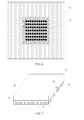
- FIG. 1 shows a top view of a chip Lid electronic component package structure.
- FIG. 2 shows a schematic diagram of a cross-sectional structure of the chip Lid electronic component package structure shown in FIG. 1 along a direction of A-A'.
- circuit pins 2 of a chip (Die) 1 are connected to a substrate 4, so that the chip 1 is attached to the substrate 4.
- a conductive lid 5 is bonded to an edge of the substrate 4 by using a non-conductive adhesive 6 having a low DK (Dielectric Constant, dielectric constant), so that a shielding space is formed between the conductive lid 5 and the substrate to implement stress protection for the chip 1.
- FIG. 3 shows a schematic diagram of a coating pattern of the non-conductive adhesive 6 on the substrate. As can be known from FIG. 3 , the non-conductive adhesive 6 is applied at the edge of the substrate, and an air hole 8 is disposed, where the air hole 8 is used for ventilation of the shielding space. Further, a top of the conductive lid (Lid) 5 is bonded to the chip 1 by using a thermally conductive adhesive 7 to implement heat conduction for the chip 1.
- the low-DK non-conductive adhesive disposed between the conductive lid 5 and the substrate causes the conductive lid to present high impedance relative to the substrate.
- the high impedance causes a non-conductive adhesive slot between the conductive lid and the substrate to become a radiation structure having a great slot antenna effect. Due to the radiation structure having a slot antenna effect, the indirectly electrically connected shielding space formed between the conductive lid and the substrate does not have a good shielding effect on the high-frequency EMI generated by the chip, although the shielding space can have a good heat conduction effect and provide stress protection for the chip in the shielding space.
- Embodiments of the present invention provide an electronic component package structure and an electronic device to improve an EMI shielding effect.
- an electronic component package structure includes a substrate, a conductive lid, and a non-conductive adhesive, where:
- the bonding end occupies all areas except the attachment area on a surface of one side of the substrate facing the conductive lid, and all the areas occupied by the bonding end on the substrate are coated with the non-conductive adhesive.
- the electronic component package structure further includes a solder mask disposed on the surface of the one side of the substrate facing the conductive lid; and in the solder mask, an open window is disposed in a position in which the non-conductive adhesive is disposed.
- the non-conductive adhesive has a closed non-conductive adhesive pattern.
- a circular, quasi-circular, or polygonal air hole is disposed in the sidewall of the conductive lid.
- an air hole is disposed in the non-conductive adhesive; and a width of the air hole along a planar direction of the substrate is not greater than 3 mm.
- the solder mask is disposed on the surface of the one side of the substrate facing the conductive lid, and in the solder mask, an open window is disposed in a position in which the air hole is disposed.
- a dielectric structure forming a filter structure is further disposed between the bonding end and the substrate, where the dielectric structure includes an electromagnetic band gap EBG and an embedded capacitor.
- a dielectric structure forming a planar capacitance structure is further disposed between the conductive lid and the substrate, where the dielectric structure includes an electromagnetic band gap EBG and an embedded capacitor.
- the electronic component is a chip or a discrete component.
- the electronic component is a chip and a discrete component.
- an electronic device includes a circuit board, an electronic component package structure, and an electronic component, where:
- a non-conductive adhesive for bonding a conductive lid to a substrate has a dielectric constant not less than 7 and a coating thickness not greater than 0.07 mm. Therefore, planar capacitance intensity of a planar capacitance structure formed by the conductive lid, the non-conductive adhesive, and the substrate is increased, and further, planar capacitance of the planar capacitance structure formed by the conductive lid, the non-conductive adhesive, and the substrate can be increased. Therefore, EMI radiated due to a slot antenna effect at the non-conductive adhesive can be reduced effectively, and an EMI shielding effect of a shielding space formed between the conductive lid and the substrate can be improved.
- the embodiments of the present invention provide an electronic component package structure having an EMI shielding effect.
- EMI shielding effect By increasing planar capacitance intensity of a planar capacitance structure formed by a conductive lid, a non-conductive adhesive, and a substrate, and increasing planar capacitance of the planar capacitance structure formed by the conductive lid, the non-conductive adhesive, and the substrate, EMI radiated due to a slot antenna effect at the non-conductive adhesive can be reduced effectively, and an EMI shielding effect of a shielding space formed between the conductive lid and the substrate can be improved.
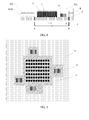
- FIG. 4 shows a top view of an electronic component package structure having an EMI shielding effect according to this embodiment of the present invention
- FIG. 5 shows a schematic diagram of a cross-sectional structure of the electronic component package structure shown in FIG. 4 along a direction of A-A'.
- the electronic component package structure provided by this embodiment of the present invention includes an electronic component (a chip or a discrete component) 1, circuit pins 2, a solder mask 3, a substrate 4, a conductive lid 5, a non-conductive adhesive 6 disposed between the substrate 4 and the conductive lid 5, and a thermally conductive adhesive 7.
- the substrate 4 has a set attachment area S for attaching an electronic component, where a size and a shape of the attachment area S may be set according to a size and a shape of an actually packaged electronic component.
- the attachment area S may be set to be slightly greater than the size of the electronic component, so that a gap exists between the electronic component and the non-conductive adhesive, where the gap should be as small as possible.
- the conductive lid 5 has a top 501 and a sidewall 502 that extends toward the substrate, where one side of the sidewall close to the substrate has a bonding end 5020, where the bonding end 5020 bonds the conductive lid 5 to the substrate 4 by using the non-conductive adhesive 6, and the conductive lid 5 bonded to the substrate 4 encloses the attachment area S set on the substrate 4 and forms a shielding space over the attachment area S to implement stress protection for the electronic component 1 attached to the substrate.
- the non-conductive adhesive 6 is disposed between the substrate and the bonding end and configured to bond the conductive lid 5 to the substrate 4, and has a dielectric constant not less than 7 and a coating thickness not greater than 0.07 mm.
- the dielectric constant of the non-conductive adhesive 6 is not less than 7. Therefore, in comparison with a conventional low-DK non-conductive adhesive, the non-conductive adhesive 6 in this embodiment of the present invention is a high-DK non-conductive adhesive.
- a high-DK non-conductive adhesive instead of a low-DK non-conductive adhesive in a conventional electronic component package structure, is used, which can increase planar capacitance intensity of a planar capacitance structure formed by the conductive lid 5, the non-conductive adhesive 6, and the substrate 4.
- the present invention can increase planar capacitance of the planar capacitance structure formed by the conductive lid, the non-conductive adhesive, and the substrate, and help to improve an EMI shielding effect of the shielding space formed between the conductive lid and the substrate.
- the dielectric constant of the non-conductive adhesive is not less than 7.
- the dielectric constant of the non-conductive adhesive in this embodiment of the present invention may be 8 or 10.
- shapes of the conductive lid 5 shown in FIG. 4 and FIG. 5 in this embodiment of the present invention are used only for exemplary description, and are not limited.
- the shapes may also be shapes shown in FIG. 7 and FIG. 8 .
- the electronic component is a chip
- the electronic component may also be another electronic component, for example, a discrete component such as a capacitor.
- the high-DK non-conductive adhesive that can increase the planar capacitance intensity of the planar capacitance structure formed by the conductive lid, the non-conductive adhesive, and the substrate is disposed to bond the conductive lid to the substrate.
- the high-DK non-conductive adhesive for bonding the conductive lid to the substrate in this embodiment of the present invention is equivalent to increasing ⁇ , and therefore, the planar capacitance of the planar capacitance structure formed by the conductive lid, the non-conductive adhesive, and the substrate can be increased.
- the coating thickness of the non-conductive adhesive is not greater than 0.07, so that parasitic inductance of the conductive lid relative to the substrate is reduced.
- EMI radiated due to a slot antenna effect at the non-conductive adhesive can be reduced effectively, and the EMI shielding effect of the shielding space formed by the planar capacitance structure formed by the conductive lid, the non-conductive adhesive, and the substrate can be improved.
- the bonding end occupies all areas except the attachment area on a surface of one side of the substrate facing the conductive lid, and all the areas occupied by the bonding end on the substrate are coated with the non-conductive adhesive.
- an overlap area between the bonding end of the sidewall of the conductive lid 5 and the substrate 4 is increased, and all the areas occupied by the bonding end on the substrate 4 are coated with the high-DK non-conductive adhesive for bonding the conductive lid 5 to the substrate 4.
- the coating area of the high-DK non-conductive adhesive can be increased, and further the planar capacitance of the planar capacitance structure formed by the conductive lid, the non-conductive adhesive, and the substrate can be increased. Further, the shielding effect of the shielding space formed between the conductive lid and the substrate is improved.
- the electronic component package structure further includes the solder mask 3 disposed on the surface of the one side of the substrate facing the conductive lid.
- the solder mask 3 in the solder mask 3, an open window is disposed in an area coated with the non-conductive adhesive, that is, the solder mask in a position coated with the high-DK non-conductive adhesive on the substrate is removed.
- the solder mask 3 is generally a low-DK green solder mask.
- the low-DK solder mask 3 is disposed at the high-DK non-conductive adhesive, which can reduce the planar capacitance intensity of the planar capacitance structure formed by the conductive lid, the non-conductive adhesive, and the substrate, and further increase a distance between the bonding end of the conductive lid and the substrate.
- the capacitance calculation formula C ⁇ s/4 ⁇ kd
- the solder mask disposed at the high-DK non-conductive adhesive can reduce planar coupling capacitance of the planar capacitance structure formed by the conductive lid, the non-conductive adhesive, and the substrate.
- the open window is disposed in the area coated with the non-conductive adhesive, which can further increase the planar capacitance of the planar capacitance structure formed by the conductive lid, the non-conductive adhesive, and the substrate. Therefore, EMI radiated due to a slot antenna effect at the non-conductive adhesive can be reduced effectively, and the EMI shielding effect of the shielding space formed between the conductive lid and the substrate can be improved.
- a coating thickness set for the high-DK non-conductive adhesive is required to be as thin as possible, for example, not greater than 0.07 mm.
- a smaller thickness of the high-DK non-conductive adhesive indicates larger planar capacitance intensity of the planar capacitance structure formed by the conductive lid, the non-conductive adhesive, and the substrate is greater.
- the capacitance intensity of the planar capacitance structure formed by the conductive lid, the non-conductive adhesive, and the substrate may exceed 75 pF/cm 2 (75 pF per square centimeter); if the dielectric constant of the non-conductive adhesive is 8 and the coating thickness is 0.06 mm, the capacitance intensity of the planar capacitance structure formed by the conductive lid, the non-conductive adhesive, and the substrate may also exceed 75 pF/cm 2 .
- the coating thickness of the non-conductive adhesive 6 is set to be not greater than 0.07 mm, which can reduce the parasitic inductance of the conductive lid relative to the substrate, reduce EMI radiated due to a slot antenna effect at the non-conductive adhesive more effectively, and improve the EMI shielding effect of the shielding space formed between the conductive lid and the substrate.
- a closed conductive adhesive pattern is preferably used as a coating pattern of the high-DK non-conductive adhesive on the substrate.
- FIG. 6 again.
- an air hole is not disposed in the non-conductive adhesive in this embodiment of the present invention, which can further avoid slot field leakage, and further improve the EMI shielding effect of the shielding space formed between the conductive lid and the substrate.
- a circular air hole 8 is disposed in the conductive lid 5.
- a shape of the air hole is not limited to a circle, for example, may also be a quasi-circular air hole (an air hole similar to a circle), or a polygonal air hole such as a rectangle.
- the air hole 8 is disposed in the sidewall of the conductive lid 5, as shown in FIG. 4, FIG. 5 , FIG. 7 , and FIG. 8 .
- the air hole 8 is disposed on the sidewall of the conductive lid 5 that extends toward the substrate, but is not disposed on a top of the conductive lid 5, which can avoid an impact of a radiator disposed on the top of the conductive lid, on disposing the air hole.
- the air hole disposed in the sidewall of the conductive lid 5 is preferably a circular air hole or a quasi-circular air hole. In comparison with a bar air hole disposed in the conventional non-conductive adhesive, a cross-sectional area is larger and ventilation is better. In addition, in comparison with an original air hole that has a larger width and is disposed in the non-conductive adhesive, the circular air hole has smaller slot field leakage.
- a chip may be attached to an attachment area set on a substrate 4, and another discrete component, for example, an electronic component such as a capacitor, a resistor, or a transistor, may also be disposed in the attachment area.
- another discrete component for example, an electronic component such as a capacitor, a resistor, or a transistor, may also be disposed in the attachment area.
- an electronic component package structure in which a chip, a discrete component, or a chip and a discrete component are attached to the attachment area set on the substrate 4 is basically the same as that in the foregoing embodiment. That is, a non-conductive adhesive has a high DK value, and a coating area of the high-DK non-conductive adhesive on the substrate is as large as possible.
- FIG. 7 is a top view of an electronic component package structure in which a chip and a discrete component are disposed in an attachment area of a substrate according to this embodiment of the present invention
- FIG. 8 shows a schematic diagram of a cross-sectional structure of the electronic component package structure shown in FIG. 7 along a direction of A-A' according to this embodiment of the present invention.
- FIG. 8 shows a schematic diagram of a cross section of the electronic component package structure in which another discrete component in addition to a chip is disposed in the attachment area according to this embodiment of the present invention.
- an air hole 8 is disposed in a conductive lid 5
- a reference number 9 represents a disposed discrete component.
- a shielding space formed between the conductive lid 5 and the substrate 4 becomes larger, and a coating pattern of the high-DK non-conductive adhesive is also changed from a regular geometric pattern to an irregular geometric pattern shown in FIG. 9 .
- FIG. 9 shows a coating pattern of a high-DK non-conductive adhesive when another discrete component is disposed in the attachment area according to this embodiment of the present invention.
- the electronic component package structure having an EMI shielding effect according to this embodiment of the present invention not only is applicable to packaging of a discrete chip, but also is applicable to mixed packaging of discrete components and multiple chips. Therefore, it is applicable in a wide scope.
- another dielectric structure forming a filter structure may be further disposed between a bonding end of the conductive lid 5 and the substrate 4, where the dielectric structure forming the filter structure may be an EBG (Electromagnetic Band gap, electromagnetic band gap), an embedded capacitor, or the like.
- EBG Electromagnetic Band gap, electromagnetic band gap
- the dielectric structure forming the filter structure in this embodiment of the present invention is not limited to the EBG or the embedded capacitor.
- another dielectric structure forming a planar capacitance structure may be further disposed between the bonding end of the conductive lid and the substrate, where the dielectric structure may be an EBG (Electromagnetic Band gap, electromagnetic band gap), an embedded capacitor, or the like.
- the dielectric structure forming the planar capacitance structure in this embodiment of the present invention is not limited to the EBG or the embedded capacitor.
- an air hole 8 may be reserved in a high-DK non-conductive adhesive, that is, an air hole is disposed in the high-DK non-conductive adhesive.
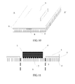
- FIG. 10 and FIG. 11 show a schematic diagram of a cross-sectional structure of the electronic component package structure shown in FIG. 10 along a direction of A-A'.
- a width of the air hole 8 disposed in the high-DK non-conductive adhesive along a planar direction of a substrate is preferably not greater than 3 mm, to reduce slot field leakage on a basis of ensuring process reliability.
- FIG. 12 is a coating pattern of a non-conductive adhesive when a small air hole is disposed in the high-DK non-conductive adhesive according to this embodiment of the present invention.
- a small air hole is disposed in the non-conductive adhesive; therefore, the coating pattern of the non-conductive adhesive is an unclosed pattern.
- the small air hole 8 is disposed in the high-DK non-conductive adhesive, and a small air hole may be disposed on a basis of an original manufacturing process. Therefore, process modification is small and process reliability can be improved.
- a chip may be attached in an attachment area set on a substrate 4, and another discrete component, for example, an electronic component such as a capacitor, a resistor, or a transistor, may also be disposed in the attachment area, and further, a chip and a discrete component may be attached in the attachment area.
- an electronic component package structure provided by this embodiment of the present invention, an electronic component package structure in which a chip, a discrete component, or a chip and a discrete component are attached is basically the same as that in the foregoing embodiment. That is, a non-conductive adhesive has a high DK value, and a coating area of the high-DK non-conductive adhesive on the substrate is as large as possible.
- FIG. 13 is a top view of an electronic component package structure in which a chip and a discrete component are disposed in an attachment area of a substrate according to this embodiment of the present invention.
- FIG. 14 shows a schematic diagram of a cross-sectional structure of the electronic component package structure shown in FIG. 13 along a direction of A-A' according to this embodiment of the present invention.
- FIG. 14 shows a schematic diagram of a cross section of an electronic component package structure in which a discrete component in addition to a chip is disposed in an attachment area according to this embodiment of the present invention.
- a reference number 1 represents the disposed chip
- a reference number 9 represents the disposed discrete component
- an air hole 8 is disposed in a non-conductive adhesive 6.
- a coating pattern of a high-DK non-conductive adhesive is changed from a regular geometric pattern shown in FIG. 12 into an irregular geometric pattern shown in FIG. 15 .
- FIG. 15 is a coating pattern of a non-conductive adhesive when a via hole is disposed in the non-conductive adhesive and a discrete component and a chip are attached to an attachment area according to this embodiment of the present invention.
- the electronic component package structure provided by this embodiment of the present invention is applicable to packaging of an electronic component package structure in which only a chip is attached, and is also applicable, and is further applicable to mixed packaging of discrete components and multiple chips. Therefore, it is applicable in a wide scope.
- another dielectric structure forming a filter structure may be further disposed between a conductive lid 5 and the substrate 4, where the dielectric structure forming the filter structure may be an EBG (Electromagnetic Band gap, electromagnetic band gap), an embedded capacitor, or the like.
- EBG Electromagnetic Band gap, electromagnetic band gap
- the dielectric structure forming the filter structure in this embodiment of the present invention is not limited to the EBG or the embedded capacitor.
- another dielectric structure forming a planar capacitance structure may be further disposed between a bonding end of the conductive lid and the substrate, where the dielectric structure may be an EBG (Electromagnetic Band gap, electromagnetic band gap), an embedded capacitor, or the like.
- the dielectric structure forming the planar capacitance structure in this embodiment of the present invention is not limited to the EBG or the embedded capacitor.
- the electronic component package structure provided by this embodiment of the present invention uses a high-DK non-conductive adhesive, which cost less in comparison with a conductive adhesive formed by a mixture of conductive materials. Further, during an assembly process of an electronic component package structure, an interior of a conductive adhesive is prone to breaking and delamination, resulting in severe deterioration of a shielding effect of a shielding space and finally causing an increase of a ratio of defective products. However, with respect to the non-conductive adhesive used by the present invention, even if breaking and delamination occur in the non-conductive adhesive, there is no impact on the EMI shielding effect of the shielding space, and a ratio of good products is increased.
- this embodiment of the present invention further provides an electronic device.
- the electronic device includes a circuit board having an electronic circuit, an electronic component package structure, and an electronic component.
- the electronic package structure in this embodiment of the present invention is any one electronic component package structure involved in the embodiments.
- the electronic component package structure is electrically connected to the circuit board by using a substrate.
- the electronic component is attached to a set attachment area in the electronic package structure, and electrically connected to the electronic circuit of the circuit board by using the electronic package structure.
- the electronic component package structure in the electronic device provided by this embodiment of the present invention is any one electronic component package structure involved in the foregoing embodiments of the present invention.
- the electronic component to be packaged is packaged on the circuit board, and therefore, a connection between the electronic component and the electronic circuit is implemented, and stress protection and proper EMI shielding can be implemented for the electronic component by using a conductive lid of the electronic component package structure.
- the electronic component in this embodiment of the present invention may be a chip, and certainly may also be another discrete component such as a capacitor, a resistor, a transistor, or the like, and certainly, a chip and a discrete component may be packaged in combination.
- the electronic component package structure having an EMI shielding effect according to this embodiment of the present invention not only is applicable to packaging of a discrete chip, but also is applicable to mixed packaging of discrete components and multiple chips. Therefore, it is applicable in a wide scope.
- a high-DK non-conductive adhesive is used in the electronic component package structure in the electronic device provided by this embodiment of the present invention. Therefore, planar capacitance intensity of a planar capacitance structure formed by the conductive lid, the non-conductive adhesive, and the substrate is increased, and further, planar capacitance of the planar capacitance structure formed by the conductive lid, the non-conductive adhesive, and the substrate can be increased. Therefore, EMI radiated due to a slot antenna effect at the non-conductive adhesive can be reduced effectively, and an EMI shielding effect of a shielding space formed between the conductive lid and the substrate can be improved.
- a high-DK non-conductive adhesive is used in this embodiment of the present invention, which cost less in comparison with a conductive adhesive formed by a mixture of conductive materials. Still further, during an assembly process of an electronic component package structure, an interior of a conductive adhesive is prone to breaking and delamination, resulting in severe deterioration of a shielding effect of a shielding space and finally causing an increase of a ratio of defective products.
- the non-conductive adhesive used by the present invention even if breaking and delamination occur in the non-conductive adhesive, there is no impact on the EMI shielding effect of the shielding space, and a ratio of good products is increased.
Landscapes
- Engineering & Computer Science (AREA)
- Microelectronics & Electronic Packaging (AREA)
- Physics & Mathematics (AREA)
- Electromagnetism (AREA)
- Shielding Devices Or Components To Electric Or Magnetic Fields (AREA)
- Health & Medical Sciences (AREA)
- Toxicology (AREA)
Applications Claiming Priority (1)
| Application Number | Priority Date | Filing Date | Title |
|---|---|---|---|
| CN201410152507.9A CN103943610B (zh) | 2014-04-16 | 2014-04-16 | 一种电子元件封装结构及电子设备 |
Publications (2)
| Publication Number | Publication Date |
|---|---|
| EP2933834A1 true EP2933834A1 (de) | 2015-10-21 |
| EP2933834B1 EP2933834B1 (de) | 2017-03-01 |
Family
ID=51191207
Family Applications (1)
| Application Number | Title | Priority Date | Filing Date |
|---|---|---|---|
| EP15163414.4A Active EP2933834B1 (de) | 2014-04-16 | 2015-04-13 | Gehäusestruktur für elektronische komponente und elektronische vorrichtung |
Country Status (4)
| Country | Link |
|---|---|
| US (2) | US9839167B2 (de) |
| EP (1) | EP2933834B1 (de) |
| CN (1) | CN103943610B (de) |
| ES (1) | ES2625170T3 (de) |
Families Citing this family (14)
| Publication number | Priority date | Publication date | Assignee | Title |
|---|---|---|---|---|
| CN103943610B (zh) * | 2014-04-16 | 2016-12-07 | 华为技术有限公司 | 一种电子元件封装结构及电子设备 |
| RU2701165C2 (ru) * | 2015-06-04 | 2019-09-25 | Хуавэй Текнолоджиз Ко., Лтд. | Мобильный терминал и теплоотводящая и экранирующая конструкция |
| DE112018001014B4 (de) * | 2017-03-30 | 2025-01-30 | Hitachi Astemo, Ltd. | Elektronische steuervorrichtung |
| WO2018182643A1 (en) * | 2017-03-30 | 2018-10-04 | Intel Corporation | Three-dimensional decoupling integration within hole in motherboard |
| EP3439028A1 (de) * | 2017-08-03 | 2019-02-06 | Siemens Aktiengesellschaft | Leistungsmodul mit mindestens einem leistungshalbleiter |
| KR102019349B1 (ko) * | 2017-10-19 | 2019-09-09 | 삼성전자주식회사 | 반도체 패키지 |
| KR102442131B1 (ko) | 2018-01-26 | 2022-09-13 | 삼성전자 주식회사 | 안테나 장치 및 안테나 장치를 포함하는 전자 장치 |
| US20200036081A1 (en) * | 2018-07-30 | 2020-01-30 | Innolux Corporation | Package structure and antenna device using the same |
| CN109637808B (zh) * | 2019-01-11 | 2024-02-23 | 芯百特微电子(无锡)有限公司 | 一种新型电容器及装置 |
| US11289433B2 (en) * | 2019-01-14 | 2022-03-29 | Advanced Semiconductor Engineering, Inc. | Semiconductor device packages and methods of manufacturing the same |
| US11089712B2 (en) * | 2019-03-19 | 2021-08-10 | Microsoft Technology Licensing, Llc | Ventilated shield can |
| CN113823622A (zh) * | 2020-06-18 | 2021-12-21 | 华为技术有限公司 | 芯片封装器件及电子设备 |
| CN116670807A (zh) * | 2020-12-28 | 2023-08-29 | 华为技术有限公司 | 封装芯片及芯片的封装方法 |
| CN118676123B (zh) * | 2024-07-19 | 2025-01-28 | 深圳市安信达存储技术有限公司 | 用于外太空的封装晶圆的封装模块及其封装方法 |
Citations (3)
| Publication number | Priority date | Publication date | Assignee | Title |
|---|---|---|---|---|
| EP0806891A1 (de) * | 1996-05-08 | 1997-11-12 | W.L. GORE & ASSOCIATES, INC. | Deckelkonstruktion zum Abschirmen von elektronischen Bauteile gegen elektromagnetische Störungen |
| US20020113306A1 (en) * | 2001-02-19 | 2002-08-22 | Kwon Heung Kyu | Semiconductor packages |
| US20100096711A1 (en) * | 2008-10-16 | 2010-04-22 | Lingsen Precision Industries, Ltd. | Microelectromechanical system microphone package |
Family Cites Families (19)
| Publication number | Priority date | Publication date | Assignee | Title |
|---|---|---|---|---|
| US4996097A (en) | 1989-03-16 | 1991-02-26 | W. L. Gore & Associates, Inc. | High capacitance laminates |
| US5387480A (en) * | 1993-03-08 | 1995-02-07 | Dow Corning Corporation | High dielectric constant coatings |
| US5761053A (en) | 1996-05-08 | 1998-06-02 | W. L. Gore & Associates, Inc. | Faraday cage |
| US6051888A (en) | 1997-04-07 | 2000-04-18 | Texas Instruments Incorporated | Semiconductor package and method for increased thermal dissipation of flip-chip semiconductor package |
| US6136128A (en) * | 1998-06-23 | 2000-10-24 | Amerasia International Technology, Inc. | Method of making an adhesive preform lid for electronic devices |
| US6614102B1 (en) * | 2001-05-04 | 2003-09-02 | Amkor Technology, Inc. | Shielded semiconductor leadframe package |
| US6740959B2 (en) | 2001-08-01 | 2004-05-25 | International Business Machines Corporation | EMI shielding for semiconductor chip carriers |
| US6956285B2 (en) | 2003-01-15 | 2005-10-18 | Sun Microsystems, Inc. | EMI grounding pins for CPU/ASIC chips |
| CN100454533C (zh) * | 2003-04-15 | 2009-01-21 | 波零公司 | 用于电子元件封装的emi屏蔽 |
| US8178956B2 (en) * | 2007-12-13 | 2012-05-15 | Stats Chippac Ltd. | Integrated circuit package system for shielding electromagnetic interference |
| CN102118674B (zh) * | 2010-01-05 | 2016-02-10 | 歌尔声学股份有限公司 | 一种mems麦克风及其封装方法 |
| CA2704683A1 (en) | 2010-05-28 | 2010-08-12 | Ibm Canada Limited - Ibm Canada Limitee | Grounded lid for micro-electronic assemblies |
| KR101855294B1 (ko) * | 2010-06-10 | 2018-05-08 | 삼성전자주식회사 | 반도체 패키지 |
| KR20120053332A (ko) * | 2010-11-17 | 2012-05-25 | 삼성전자주식회사 | 반도체 패키지 및 이의 제조 방법 |
| JP5512566B2 (ja) * | 2011-01-31 | 2014-06-04 | 株式会社東芝 | 半導体装置 |
| CN102779811B (zh) | 2012-07-20 | 2015-02-04 | 华为技术有限公司 | 一种芯片封装及封装方法 |
| US9129954B2 (en) * | 2013-03-07 | 2015-09-08 | Advanced Semiconductor Engineering, Inc. | Semiconductor package including antenna layer and manufacturing method thereof |
| CN103943610B (zh) * | 2014-04-16 | 2016-12-07 | 华为技术有限公司 | 一种电子元件封装结构及电子设备 |
| US9401682B2 (en) * | 2014-04-17 | 2016-07-26 | Freescale Semiconductor, Inc. | Structure for a radio frequency power amplifier module within a radio frequency power amplifier package |
-
2014
- 2014-04-16 CN CN201410152507.9A patent/CN103943610B/zh active Active
-
2015
- 2015-04-13 EP EP15163414.4A patent/EP2933834B1/de active Active
- 2015-04-13 ES ES15163414.4T patent/ES2625170T3/es active Active
- 2015-04-15 US US14/687,511 patent/US9839167B2/en active Active
-
2017
- 2017-10-23 US US15/790,992 patent/US10091915B2/en active Active
Patent Citations (3)
| Publication number | Priority date | Publication date | Assignee | Title |
|---|---|---|---|---|
| EP0806891A1 (de) * | 1996-05-08 | 1997-11-12 | W.L. GORE & ASSOCIATES, INC. | Deckelkonstruktion zum Abschirmen von elektronischen Bauteile gegen elektromagnetische Störungen |
| US20020113306A1 (en) * | 2001-02-19 | 2002-08-22 | Kwon Heung Kyu | Semiconductor packages |
| US20100096711A1 (en) * | 2008-10-16 | 2010-04-22 | Lingsen Precision Industries, Ltd. | Microelectromechanical system microphone package |
Also Published As
| Publication number | Publication date |
|---|---|
| US20180049351A1 (en) | 2018-02-15 |
| EP2933834B1 (de) | 2017-03-01 |
| US10091915B2 (en) | 2018-10-02 |
| CN103943610A (zh) | 2014-07-23 |
| US9839167B2 (en) | 2017-12-05 |
| ES2625170T3 (es) | 2017-07-18 |
| CN103943610B (zh) | 2016-12-07 |
| US20150305210A1 (en) | 2015-10-22 |
Similar Documents
| Publication | Publication Date | Title |
|---|---|---|
| US10091915B2 (en) | Electronic component package structure and electronic device | |
| TWI552434B (zh) | 具有天線之半導體結構 | |
| US9101050B2 (en) | Circuit module having electrical shield | |
| US20100110656A1 (en) | Chip package and manufacturing method thereof | |
| CN107305884B (zh) | 具有虚拟接地能力的板级屏蔽件 | |
| CN110349919A (zh) | 电子器件模块及制造该电子器件模块的方法 | |
| US9018039B2 (en) | Circuit module and method of producing circuit module | |
| US20240194615A1 (en) | Integrated shield package and method | |
| EP2618371B1 (de) | Halbleiterbauelement | |
| US9484311B2 (en) | Chip package and packaging method | |
| US20140098499A1 (en) | Electronic device, structure, and heat sink | |
| US20150085462A1 (en) | Electromagnetic interference shielding material, electromagnetic interference shielding device, method for making the electromagnetic interference shielding device, electromagnetic interference shielding package module and appliance | |
| CN101937905B (zh) | 半导体封装件与其制造方法 | |
| CN210489609U (zh) | 集成电路封装体 | |
| WO2012101857A1 (ja) | モジュール基板 | |
| US9041169B2 (en) | Semiconductor packaging container, semiconductor device, electronic device | |
| KR101994714B1 (ko) | 고주파 모듈 | |
| US11744019B2 (en) | Component mounted on circuit board | |
| KR101971282B1 (ko) | 대역 저지 필터를 구비하는 패키지 기판 및 이를 포함하는 반도체 패키지 | |
| KR101940295B1 (ko) | 전자파 차폐막을 구비한 기판 구조체 | |
| US20150170825A1 (en) | Planar Transformer and Electrical Component | |
| KR20140095360A (ko) | 보호 케이스 및 이를 포함한 전자소자 패키지 | |
| HK1204390B (zh) | 电路模块以及电路模块的制造方法 | |
| JPH1065058A (ja) | 半導体パッケージ型素子およびその実装構造体 |
Legal Events
| Date | Code | Title | Description |
|---|---|---|---|
| PUAI | Public reference made under article 153(3) epc to a published international application that has entered the european phase |
Free format text: ORIGINAL CODE: 0009012 |
|
| AK | Designated contracting states |
Kind code of ref document: A1 Designated state(s): AL AT BE BG CH CY CZ DE DK EE ES FI FR GB GR HR HU IE IS IT LI LT LU LV MC MK MT NL NO PL PT RO RS SE SI SK SM TR |
|
| AX | Request for extension of the european patent |
Extension state: BA ME |
|
| 17P | Request for examination filed |
Effective date: 20160421 |
|
| RBV | Designated contracting states (corrected) |
Designated state(s): AL AT BE BG CH CY CZ DE DK EE ES FI FR GB GR HR HU IE IS IT LI LT LU LV MC MK MT NL NO PL PT RO RS SE SI SK SM TR |
|
| REG | Reference to a national code |
Ref country code: DE Ref legal event code: R079 Ref document number: 602015001600 Country of ref document: DE Free format text: PREVIOUS MAIN CLASS: H01L0023552000 Ipc: H05K0001020000 |
|
| GRAJ | Information related to disapproval of communication of intention to grant by the applicant or resumption of examination proceedings by the epo deleted |
Free format text: ORIGINAL CODE: EPIDOSDIGR1 |
|
| RIC1 | Information provided on ipc code assigned before grant |
Ipc: H05K 1/02 20060101AFI20160803BHEP Ipc: H01L 23/552 20060101ALI20160803BHEP Ipc: H05K 1/18 20060101ALI20160803BHEP Ipc: H05K 9/00 20060101ALI20160803BHEP Ipc: H01L 23/10 20060101ALI20160803BHEP |
|
| GRAP | Despatch of communication of intention to grant a patent |
Free format text: ORIGINAL CODE: EPIDOSNIGR1 |
|
| INTG | Intention to grant announced |
Effective date: 20160909 |
|
| RIN1 | Information on inventor provided before grant (corrected) |
Inventor name: YANG, LIN Inventor name: BAI, YADONG Inventor name: YU, XUEQUAN |
|
| GRAS | Grant fee paid |
Free format text: ORIGINAL CODE: EPIDOSNIGR3 |
|
| GRAA | (expected) grant |
Free format text: ORIGINAL CODE: 0009210 |
|
| AK | Designated contracting states |
Kind code of ref document: B1 Designated state(s): AL AT BE BG CH CY CZ DE DK EE ES FI FR GB GR HR HU IE IS IT LI LT LU LV MC MK MT NL NO PL PT RO RS SE SI SK SM TR |
|
| REG | Reference to a national code |
Ref country code: GB Ref legal event code: FG4D |
|
| REG | Reference to a national code |
Ref country code: FR Ref legal event code: PLFP Year of fee payment: 3 |
|
| REG | Reference to a national code |
Ref country code: CH Ref legal event code: EP Ref country code: AT Ref legal event code: REF Ref document number: 872666 Country of ref document: AT Kind code of ref document: T Effective date: 20170315 |
|
| REG | Reference to a national code |
Ref country code: IE Ref legal event code: FG4D |
|
| REG | Reference to a national code |
Ref country code: DE Ref legal event code: R096 Ref document number: 602015001600 Country of ref document: DE |
|
| REG | Reference to a national code |
Ref country code: NL Ref legal event code: FP |
|
| REG | Reference to a national code |
Ref country code: SE Ref legal event code: TRGR |
|
| REG | Reference to a national code |
Ref country code: LT Ref legal event code: MG4D |
|
| REG | Reference to a national code |
Ref country code: AT Ref legal event code: MK05 Ref document number: 872666 Country of ref document: AT Kind code of ref document: T Effective date: 20170301 |
|
| REG | Reference to a national code |
Ref country code: ES Ref legal event code: FG2A Ref document number: 2625170 Country of ref document: ES Kind code of ref document: T3 Effective date: 20170718 |
|
| PG25 | Lapsed in a contracting state [announced via postgrant information from national office to epo] |
Ref country code: HR Free format text: LAPSE BECAUSE OF FAILURE TO SUBMIT A TRANSLATION OF THE DESCRIPTION OR TO PAY THE FEE WITHIN THE PRESCRIBED TIME-LIMIT Effective date: 20170301 Ref country code: NO Free format text: LAPSE BECAUSE OF FAILURE TO SUBMIT A TRANSLATION OF THE DESCRIPTION OR TO PAY THE FEE WITHIN THE PRESCRIBED TIME-LIMIT Effective date: 20170601 Ref country code: LT Free format text: LAPSE BECAUSE OF FAILURE TO SUBMIT A TRANSLATION OF THE DESCRIPTION OR TO PAY THE FEE WITHIN THE PRESCRIBED TIME-LIMIT Effective date: 20170301 Ref country code: GR Free format text: LAPSE BECAUSE OF FAILURE TO SUBMIT A TRANSLATION OF THE DESCRIPTION OR TO PAY THE FEE WITHIN THE PRESCRIBED TIME-LIMIT Effective date: 20170602 |
|
| PG25 | Lapsed in a contracting state [announced via postgrant information from national office to epo] |
Ref country code: LV Free format text: LAPSE BECAUSE OF FAILURE TO SUBMIT A TRANSLATION OF THE DESCRIPTION OR TO PAY THE FEE WITHIN THE PRESCRIBED TIME-LIMIT Effective date: 20170301 Ref country code: AT Free format text: LAPSE BECAUSE OF FAILURE TO SUBMIT A TRANSLATION OF THE DESCRIPTION OR TO PAY THE FEE WITHIN THE PRESCRIBED TIME-LIMIT Effective date: 20170301 Ref country code: RS Free format text: LAPSE BECAUSE OF FAILURE TO SUBMIT A TRANSLATION OF THE DESCRIPTION OR TO PAY THE FEE WITHIN THE PRESCRIBED TIME-LIMIT Effective date: 20170301 Ref country code: BG Free format text: LAPSE BECAUSE OF FAILURE TO SUBMIT A TRANSLATION OF THE DESCRIPTION OR TO PAY THE FEE WITHIN THE PRESCRIBED TIME-LIMIT Effective date: 20170601 |
|
| PG25 | Lapsed in a contracting state [announced via postgrant information from national office to epo] |
Ref country code: EE Free format text: LAPSE BECAUSE OF FAILURE TO SUBMIT A TRANSLATION OF THE DESCRIPTION OR TO PAY THE FEE WITHIN THE PRESCRIBED TIME-LIMIT Effective date: 20170301 Ref country code: RO Free format text: LAPSE BECAUSE OF FAILURE TO SUBMIT A TRANSLATION OF THE DESCRIPTION OR TO PAY THE FEE WITHIN THE PRESCRIBED TIME-LIMIT Effective date: 20170301 Ref country code: SK Free format text: LAPSE BECAUSE OF FAILURE TO SUBMIT A TRANSLATION OF THE DESCRIPTION OR TO PAY THE FEE WITHIN THE PRESCRIBED TIME-LIMIT Effective date: 20170301 Ref country code: CZ Free format text: LAPSE BECAUSE OF FAILURE TO SUBMIT A TRANSLATION OF THE DESCRIPTION OR TO PAY THE FEE WITHIN THE PRESCRIBED TIME-LIMIT Effective date: 20170301 |
|
| PG25 | Lapsed in a contracting state [announced via postgrant information from national office to epo] |
Ref country code: PL Free format text: LAPSE BECAUSE OF FAILURE TO SUBMIT A TRANSLATION OF THE DESCRIPTION OR TO PAY THE FEE WITHIN THE PRESCRIBED TIME-LIMIT Effective date: 20170301 Ref country code: SM Free format text: LAPSE BECAUSE OF FAILURE TO SUBMIT A TRANSLATION OF THE DESCRIPTION OR TO PAY THE FEE WITHIN THE PRESCRIBED TIME-LIMIT Effective date: 20170301 Ref country code: PT Free format text: LAPSE BECAUSE OF FAILURE TO SUBMIT A TRANSLATION OF THE DESCRIPTION OR TO PAY THE FEE WITHIN THE PRESCRIBED TIME-LIMIT Effective date: 20170703 Ref country code: IS Free format text: LAPSE BECAUSE OF FAILURE TO SUBMIT A TRANSLATION OF THE DESCRIPTION OR TO PAY THE FEE WITHIN THE PRESCRIBED TIME-LIMIT Effective date: 20170701 |
|
| REG | Reference to a national code |
Ref country code: DE Ref legal event code: R097 Ref document number: 602015001600 Country of ref document: DE |
|
| PLBE | No opposition filed within time limit |
Free format text: ORIGINAL CODE: 0009261 |
|
| STAA | Information on the status of an ep patent application or granted ep patent |
Free format text: STATUS: NO OPPOSITION FILED WITHIN TIME LIMIT |
|
| REG | Reference to a national code |
Ref country code: IE Ref legal event code: MM4A |
|
| PG25 | Lapsed in a contracting state [announced via postgrant information from national office to epo] |
Ref country code: DK Free format text: LAPSE BECAUSE OF FAILURE TO SUBMIT A TRANSLATION OF THE DESCRIPTION OR TO PAY THE FEE WITHIN THE PRESCRIBED TIME-LIMIT Effective date: 20170301 Ref country code: MC Free format text: LAPSE BECAUSE OF FAILURE TO SUBMIT A TRANSLATION OF THE DESCRIPTION OR TO PAY THE FEE WITHIN THE PRESCRIBED TIME-LIMIT Effective date: 20170301 |
|
| 26N | No opposition filed |
Effective date: 20171204 |
|
| PG25 | Lapsed in a contracting state [announced via postgrant information from national office to epo] |
Ref country code: SI Free format text: LAPSE BECAUSE OF FAILURE TO SUBMIT A TRANSLATION OF THE DESCRIPTION OR TO PAY THE FEE WITHIN THE PRESCRIBED TIME-LIMIT Effective date: 20170301 Ref country code: LU Free format text: LAPSE BECAUSE OF NON-PAYMENT OF DUE FEES Effective date: 20170413 |
|
| REG | Reference to a national code |
Ref country code: FR Ref legal event code: PLFP Year of fee payment: 4 |
|
| REG | Reference to a national code |
Ref country code: BE Ref legal event code: MM Effective date: 20170430 |
|
| PG25 | Lapsed in a contracting state [announced via postgrant information from national office to epo] |
Ref country code: IE Free format text: LAPSE BECAUSE OF NON-PAYMENT OF DUE FEES Effective date: 20170413 |
|
| PG25 | Lapsed in a contracting state [announced via postgrant information from national office to epo] |
Ref country code: BE Free format text: LAPSE BECAUSE OF NON-PAYMENT OF DUE FEES Effective date: 20170430 |
|
| PG25 | Lapsed in a contracting state [announced via postgrant information from national office to epo] |
Ref country code: MT Free format text: LAPSE BECAUSE OF NON-PAYMENT OF DUE FEES Effective date: 20170413 |
|
| REG | Reference to a national code |
Ref country code: CH Ref legal event code: PL |
|
| PG25 | Lapsed in a contracting state [announced via postgrant information from national office to epo] |
Ref country code: LI Free format text: LAPSE BECAUSE OF NON-PAYMENT OF DUE FEES Effective date: 20180430 Ref country code: CH Free format text: LAPSE BECAUSE OF NON-PAYMENT OF DUE FEES Effective date: 20180430 |
|
| PG25 | Lapsed in a contracting state [announced via postgrant information from national office to epo] |
Ref country code: HU Free format text: LAPSE BECAUSE OF FAILURE TO SUBMIT A TRANSLATION OF THE DESCRIPTION OR TO PAY THE FEE WITHIN THE PRESCRIBED TIME-LIMIT; INVALID AB INITIO Effective date: 20150413 |
|
| PG25 | Lapsed in a contracting state [announced via postgrant information from national office to epo] |
Ref country code: CY Free format text: LAPSE BECAUSE OF FAILURE TO SUBMIT A TRANSLATION OF THE DESCRIPTION OR TO PAY THE FEE WITHIN THE PRESCRIBED TIME-LIMIT Effective date: 20170301 |
|
| PG25 | Lapsed in a contracting state [announced via postgrant information from national office to epo] |
Ref country code: MK Free format text: LAPSE BECAUSE OF FAILURE TO SUBMIT A TRANSLATION OF THE DESCRIPTION OR TO PAY THE FEE WITHIN THE PRESCRIBED TIME-LIMIT Effective date: 20170301 |
|
| PG25 | Lapsed in a contracting state [announced via postgrant information from national office to epo] |
Ref country code: TR Free format text: LAPSE BECAUSE OF FAILURE TO SUBMIT A TRANSLATION OF THE DESCRIPTION OR TO PAY THE FEE WITHIN THE PRESCRIBED TIME-LIMIT Effective date: 20170301 |
|
| PG25 | Lapsed in a contracting state [announced via postgrant information from national office to epo] |
Ref country code: AL Free format text: LAPSE BECAUSE OF FAILURE TO SUBMIT A TRANSLATION OF THE DESCRIPTION OR TO PAY THE FEE WITHIN THE PRESCRIBED TIME-LIMIT Effective date: 20170301 |
|
| P01 | Opt-out of the competence of the unified patent court (upc) registered |
Free format text: CASE NUMBER: UPC_APP_327347/2023 Effective date: 20230524 |
|
| PGFP | Annual fee paid to national office [announced via postgrant information from national office to epo] |
Ref country code: FI Payment date: 20250421 Year of fee payment: 11 |
|
| PGFP | Annual fee paid to national office [announced via postgrant information from national office to epo] |
Ref country code: DE Payment date: 20250305 Year of fee payment: 11 |
|
| PGFP | Annual fee paid to national office [announced via postgrant information from national office to epo] |
Ref country code: ES Payment date: 20250509 Year of fee payment: 11 |
|
| PGFP | Annual fee paid to national office [announced via postgrant information from national office to epo] |
Ref country code: SE Payment date: 20260312 Year of fee payment: 12 |
|
| PGFP | Annual fee paid to national office [announced via postgrant information from national office to epo] |
Ref country code: GB Payment date: 20260310 Year of fee payment: 12 |
|
| PGFP | Annual fee paid to national office [announced via postgrant information from national office to epo] |
Ref country code: IT Payment date: 20260320 Year of fee payment: 12 |
|
| PGFP | Annual fee paid to national office [announced via postgrant information from national office to epo] |
Ref country code: NL Payment date: 20260317 Year of fee payment: 12 |
|
| PGFP | Annual fee paid to national office [announced via postgrant information from national office to epo] |
Ref country code: FR Payment date: 20260309 Year of fee payment: 12 |