EP2941098A2 - Leuchtdiodenbeleuchtungsvorrichtung mit mehreren ansteuerungsstufen - Google Patents
Leuchtdiodenbeleuchtungsvorrichtung mit mehreren ansteuerungsstufen Download PDFInfo
- Publication number
- EP2941098A2 EP2941098A2 EP15166108.9A EP15166108A EP2941098A2 EP 2941098 A2 EP2941098 A2 EP 2941098A2 EP 15166108 A EP15166108 A EP 15166108A EP 2941098 A2 EP2941098 A2 EP 2941098A2
- Authority
- EP
- European Patent Office
- Prior art keywords
- current
- controller
- voltage
- lighting device
- led lighting
- Prior art date
- Legal status (The legal status is an assumption and is not a legal conclusion. Google has not performed a legal analysis and makes no representation as to the accuracy of the status listed.)
- Withdrawn
Links
Images



Classifications
-
- H—ELECTRICITY
- H05—ELECTRIC TECHNIQUES NOT OTHERWISE PROVIDED FOR
- H05B—ELECTRIC HEATING; ELECTRIC LIGHT SOURCES NOT OTHERWISE PROVIDED FOR; CIRCUIT ARRANGEMENTS FOR ELECTRIC LIGHT SOURCES, IN GENERAL
- H05B45/00—Circuit arrangements for operating light-emitting diodes [LED]
- H05B45/40—Details of LED load circuits
- H05B45/44—Details of LED load circuits with an active control inside an LED matrix
Definitions
- the present invention is related to an LED lighting device having multiple driving stages, and more particularly, to an LED lighting device having multiple driving stages for providing wide effective operational voltage range without causing image flicker and uniformity issue.
- LEDs light-emitting diodes
- LCD liquid crystal display
- PDAs personal digital assistants
- An LED lighting device is normally driven by a rectified alternative-current (AC) voltage and adopts a plurality of LEDs coupled in series in order to provide required luminance.
- AC alternative-current
- the LEDs may be light up in steps in order to increase the effective operational voltage range.
- the LEDs which are turned on more frequently are aged faster than those which are turned on less frequently, thereby causing uniformity issue.
- Image flicker may also occur at low rectified AC voltage when not all LEDs are light up. Therefore, there is a need for an LED lighting device capable of improving the effective operational voltage range without causing image flicker and uniformity issue.
- the present invention provides an LED lighting device having a first driving stage and a second driving stage.
- the first driving stage includes a first luminescent device for providing light according to a first current; a second luminescent device for providing light according to a second current; a first current controller coupled in series to the first luminescent device and configured to regulate the first current so that the first current does not exceed a first value; a second current controller coupled in series to the second luminescent device and configured to regulate the second current so that the second current does not exceed a second value; a first path-controller configured to conduct a third current and comprising a first end coupled between the second luminescent device and the second current controller; and a second end coupled to the first current controller.
- the second driving stage includes a third current controller coupled in series to the first driving stage and configured to conduct a fourth current and regulate the fourth current so that the fourth current does not exceed a third value.
- a third current controller coupled in series to the first driving stage and configured to conduct a fourth current and regulate the fourth current so that the fourth current does not exceed a third value.
- Fig. 1 is a diagram of an LED lighting device 100 according to an embodiment of the present invention.
- the LED lighting device 100 includes a power supply circuit 110 and (N+1) driving stages ST 1 ⁇ ST N+1 (N is a positive integer).
- the power supply circuit 110 is configured to receive an AC voltage VS having positive and negative periods and convert the output of the AC voltage VS in the negative period using a bridge rectifier 112, thereby providing a rectified AC voltage V AC , whose value varies periodically with time, for driving the (N+1) driving stages.
- the power supply circuit 110 may receive any AC voltage VS, perform voltage conversion using an AC-AC converter, and rectify the converted AC voltage VS using the bridge rectifier 112, thereby providing the rectified AC voltage V AC whose value varies periodically with time.
- the configuration of the power supply circuit 110 does not limit the scope of the present invention.
- Each of the 1 st to N th driving stages ST 1 ⁇ ST N includes a plurality of luminescent devices, a path controller, a first-type current controller and a second-type current controller.
- the (N+1) th driving stage ST N+1 includes a third-type current controller.
- Each first-type current controller includes an adjustable current source and a current detection and control unit.
- Each second-type current controller includes an adjustable current source and a voltage detection and control unit.
- the third-type current controller includes an adjustable current source and a detection and control unit.
- a 1 ⁇ A N and B 1 ⁇ B N represent the luminescent devices in the corresponding driving stages ST 1 ⁇ ST N , respectively.
- D 1 ⁇ D N represent the path-controllers in the corresponding driving stages ST 1 ⁇ ST N , respectively.
- CCA 1 ⁇ CCA N represent the first-type current controllers in the corresponding driving stages ST 1 ⁇ ST N , respectively.
- CCB 1 ⁇ CCB N represent the second-type current controllers in the corresponding driving stages ST 1 ⁇ ST N , respectively.
- CC N+1 represents the third-type current controller in the (N+1) th driving stage ST N+1 .
- ISA 1 ⁇ ISA N represent the adjustable current sources in the corresponding first-type current controllers CCA 1 ⁇ CCA N , respectively.
- ISB 1 ⁇ ISB N represent the adjustable current sources in the corresponding second-type current controllers CCB 1 ⁇ CCB N , respectively.
- IS N+1 represents the adjustable current source in the third-type current controller CC N+1 .
- UNA 1 ⁇ UNA N represent the current detection and control units in the corresponding first-type current controllers CCA 1 ⁇ CCA N , respectively.
- UNB 1 ⁇ UNB N represent the voltage detection and control units in the corresponding second-type current controllers CCB 1 ⁇ CCB N , respectively.
- UN N+1 represents the detection and control unit in the (N+1) th driving stage ST N+1 .
- V IN1 ⁇ V INN represent the voltages established across the 1 st to N th driving stages ST 1 ⁇ ST N , respectively.
- V AK1 ⁇ V AKN represent the voltages established across the corresponding first-type current controllers CCA 1 ⁇ CCA N , respectively.
- V BK1 ⁇ V BKN represent the voltages established across the corresponding second-type current controllers CCB 1 ⁇ CCB N , respectively.
- V CK represents the voltage established across the third-type current controller CC N+1 .
- I AK1 ⁇ I AKN represent the current flowing through the corresponding first-type current controllers CCA 1 ⁇ CCA N , respectively.
- I BK1 ⁇ I BKN represent the current flowing through the corresponding second-type current controllers CCB 1 ⁇ CCB N , respectively.
- I A1 ⁇ I AN represent the current flowing through the corresponding luminescent devices A 1 ⁇ A N , respectively.
- I B1 ⁇ I BN represent the current flowing through the corresponding luminescent devices B 1 ⁇ B N , respectively.
- I D1 ⁇ I DN represent the current flowing through the corresponding path controllers D 1 ⁇ D N , respectively.
- I SUM1 ⁇ I SUMN represent the current flowing through the corresponding driving stages ST 1 ⁇ ST N , respectively.
- the overall current of the LED lighting device 100 may be represented by I SUMN .
- the current detection and control units UNA 1 ⁇ UNA N are configured to regulate the values of the adjustable current sources ISA 1 ⁇ ISA N according the current I AK1 ⁇ I AKN , respectively.
- the voltage detection and control units UNB 1 ⁇ UNB N respectively coupled in series to the corresponding luminescent devices B 1 ⁇ B N and in parallel with the corresponding adjustable current sources ISB 1 ⁇ ISB N , are configured to regulate the values of the adjustable current sources ISB 1 ⁇ ISB N according the voltages V BK1 ⁇ V BKN , respectively.
- the adjustable current source IS N+1 is coupled in series to the 1 st to N th driving stages ST 1 ⁇ ST N .
- the detection and control unit UN N+1 of the third-type current controller CC N+1 may be coupled in series to the adjustable current source IS N+1 and is configured to regulate the value of the adjustable current source IS N+1 according the current I SUMN .
- the detection and control unit UN N+1 of the third-type current controller CC N+1 may be coupled in parallel with the adjustable current source IS N+1 and is configured to regulate the value of the adjustable current source IS N+1 according the voltage V CK .
- Fig. 1 depicts the embodiment adopting the first configuration, but does not limit the scope of the present invention.
- each of the luminescent devices A 1 ⁇ A N and B 1 ⁇ B N may adopt a single LED or multiple LEDs coupled in series, in parallel, or in array.
- Fig. 1 depicts the embodiment using multiple LEDs, but do not limit the scope of the present invention.
- each of the path-controllers D 1 ⁇ D N may adopt a diode or any device providing similar function.
- the embodiment of the path-controllers D 1 ⁇ D N does not limit the scope of the present invention.
- FIGs. 2 ⁇ 5 are diagrams illustrating the operation of the 1 st to N th driving stages ST 1 ⁇ ST N .
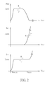
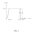
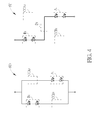
- the driving stage ST 1 is used for illustrative purpose, wherein FIG. 2 illustrates the current-voltage curve (I-V curve) of the first-type current controller CCA 1 , FIG. 3 illustrates the I-V curve of the second-type current controller CCB 1 , FIG. 4 illustrates the equivalent circuits of the 1 st driving stage ST 1 during different phases of operation, and FIG. 5 illustrates the I-V curve of the 1 st driving stage ST 1 .
- FIG. 6 is a diagram illustrating the operation of the current controller CC N+1 in the (N+1) th driving stages ST N+1 .
- V DROPA , V DROPB and V DROPC represent the drop-out voltages for turning on the first-type current controller CCA 1 , the second-type current controller CCB 1 and the third-type current controller CCB N+1 , respectively.
- V OFFA , V OFFB and V ONB represent the threshold voltages based on which the first-type current controller CCA 1 or the second-type current controller CCB 1 switch operational modes.
- I SETA1 , I SETB1 and I SETC are constant values which represent the current settings of the first-type current controller CCA 1 , the second-type current controller and the third-type current controller CC N+1 , respectively.
- An arrow R indicates the rising period of the voltage V AK1 , V BK1 or V CK .
- An arrow L indicates the falling period of the voltage V AK1 , V BK1 or V CK .
- the first-type current controller CCA 1 is not completely turned on and operates as a voltage-controlled device in a linear mode in which the current I AK1 changes with the voltage V AK1 in a specific manner.
- the current I AK1 reaches I SETA1 , and the first-type current controller CCA 1 switches to a constant-current mode and functions as a current limiter.
- the current detection and control unit UNA 1 is configured to clamp the current I AK1 at I SETA1 .
- the current detection and control unit UNA 1 may decrease the value of the adjustable current source ISA 1 accordingly.
- the current detection and control unit UNA 1 turns off the adjustable current source ISA 1 and the current controller CCA 1 switches to a cut-off mode in which the current I AK1 increases with the current I D1 .
- the current detection and control unit UNA 1 turns off the adjustable current source ISA 1 and the current controller CCA 1 operates in the cut-off mode in which the current I AK1 decreases with the current I D1 .
- the current detection and control unit UNA 1 turns on the adjustable current source ISA 1 and the current controller CCA 1 functions as a current limiter in the constant-current mode in which the current I AK1 is clamped at a constant value of I SETA1 .
- the second-type current controller CCB 1 is not completely turned on and operates as a voltage-controlled device in the linear mode in which the current I BK1 changes with the voltage V BK1 in a specific manner.
- the current I BK1 reaches I SETB1 , and the current controller CCB 1 switches to the constant-current mode and functions as a current limiter.
- the voltage detection and control unit UNB 1 is configured to clamp the current I BK1 at I SETB1 .
- the voltage detection and control unit UNB 1 is configured to turn off the adjustable current source ISB 1 and the second-type current controller CCB 1 switches to the cut-off mode.
- the second-type current controller CCB 1 functions as an open-circuited device.
- the voltage detection and control unit UNB 1 is configured to turn on the adjustable current source ISB 1 and the current controller CCB 1 switches to the constant-current mode and functions as a current limiter, thereby clamping the current I BK1 at I SETB1 .
- the threshold voltage V ONB is larger than or equal to the threshold voltage V OFFB .
- a non-zero hysteresis band (V ONB -V OFFB ) may be provided in order to prevent the second-type current controller CCB 1 from frequently switching operational modes due to fluctuations in the voltage V BK1 .
- the luminance device A 1 when the 1 st driving stage ST 1 operates in a first phase with V1 ⁇ V IN1 ⁇ V2, the luminance device A 1 is coupled in parallel with the luminance device B 1 , as depicted on the left of FIG.4 .
- the luminance device A 1 When the 1 st driving stage ST 1 operates in a second phase with V IN1 >V3, the luminance device A 1 is coupled in series to the luminance device B 1 , as depicted on the right of FIG.4 .
- the current I SUM1 is equal to the sum of the current I A1 and the current I B1 , wherein the current I A1 is regulated by the current controllers CCA 1 and the current I B1 is regulated by the current controllers CCB 1 .
- the value of the turn-on voltage V A1 may be equal to or different from that of the turn-on voltage V B1 .
- the current I SUM1 starts to increase at a voltage V1 which is equal to the smaller one among the turn-on voltage V A1 and the turn-on voltage V B1 .
- the second-type current controller CCB 1 switches to the cut-off mode in which the current I A1 is directed towards the path-controller D 1 , thereby turning on the path-controller D1.
- the current I SUM1 is equal to the current I B1 , wherein both the current I A1 and the current I B1 are regulated by the first-type current controller CCA 1 .
- the current I D1 gradually increases with the voltage V IN1 .
- the first-type current controller CCA 1 decreases the value of the adjustable current source ISA 1 accordingly, so that the overall current I AK1 is still maintained at the constant value I SETA1 .
- the first-type current controller CCA 1 switches to the cut-off mode.
- the current I SUM1 is now regulated by the subsequent driving stage.
- the third-type current controller CC N+1 is not completely turned on and operates as a voltage-controlled device in the linear mode in which the current I CK changes with the voltage V CK in a specific manner.
- the current I CK reaches I SETC , and the third-type current controller CC N+1 switches to the constant-current mode and functions as a current limiter.
- Fig. 7 is a diagram illustrating the overall operation of the LED lighting device 100 according to the present invention.
- the rectified AC voltage V AC is low and the voltages V IN1 ⁇ V IN2 are insufficient to turn on the luminescent devices A 1 ⁇ A 2 and B 1 ⁇ B 2 or the current controllers CCA 1 ⁇ CCA 2 , CCB 1 ⁇ CCB 2 and CC 3 . Therefore, all the 3 driving stages ST1 ⁇ ST3 operate in the cut-off mode, and the overall current I SUMN of the LED lighting device 100 is zero.
- all 3 driving stages ST 1 ⁇ ST 3 operate in the linear mode in which the overall current I SUMN of the LED lighting device 100 increases with the rectified AC voltage V AC in a specific manner.
- the first driving stage ST 1 switches to the cut-off mode, while the second and third driving stages ST 2 ⁇ ST 3 remain operating in the linear mode in which the overall current I SUMN of the LED lighting device 100 increases with the rectified AC voltage V AC in a specific manner.
- the second driving stage ST 2 switches to the cut-off mode, while the third driving stage ST 3 remain operating in the linear mode in which the overall current I SUMN of the LED lighting device 100 increases with the rectified AC voltage V AC in a specific manner.
- the intervals t 0 ⁇ t 1 , t 1 ⁇ t 2 , t 2 ⁇ t 3 , t 3 ⁇ t 4 and t 4 ⁇ t 5 during the rising period correspond to the intervals t 10 ⁇ t 11 , t 9 ⁇ t 10 , t 8 ⁇ t 9 , t 7 ⁇ t 8 and t 6 ⁇ t 7 during the falling period, Therefore, the operation of the LED lighting device 100 during t 6 -t 11 is similar to that during t 0 ⁇ t 5 , as detailed in previous paragraphs.
- the current settings of the LED lighting device 100 may have the following relationship: (I SETA1 +I SETB1 ) ⁇ (I SETA2 +I SETB2 ) ⁇ I SETC .
- phase 1 and phase 2 respectively represent the first phase and the second phase in the operation of the equivalent circuits of the 1 st driving stage ST 1 depicted in FIG. 4 .
- Fig. 8 is a diagram of an LED lighting device 200 according to another embodiment of the present invention. Similar to the LED lighting device 100 depicted in FIG. 1 , the LED lighting device 200 also includes a power supply circuit 110 and (N+1) driving stages ST 1 ⁇ ST N+1 (N is a positive integer). However, the LED lighting device 200 differs from the LED lighting device 100 in that each of the 1 st to N th driving stages ST 1 ⁇ ST N includes a plurality of luminescent devices, a path controller, and two first-type current controllers. Each first-type current controller includes an adjustable current source and a current detection and control unit, and its I-V curve may also be shown in FIG. 2 .
- the current detection and control units UNA 1 ⁇ UNA N are configured to regulate the values of the adjustable current sources ISA 1 ⁇ ISA N according the current I AK1 ⁇ I AKN , respectively.
- the current detection and control units UNA 1 ' ⁇ UNA N ' are configured to regulate the values of the adjustable current sources ISA 1 ' ⁇ ISA N ' according the current I BK1 ⁇ I BKN , respectively.
- the overall operation of the LED lighting device 200 may also be shown in FIG. 7 .
- the LED lighting device of the present invention may improve the effective operational voltage range without causing image flicker and uniformity issue.
Landscapes
- Circuit Arrangement For Electric Light Sources In General (AREA)
Applications Claiming Priority (1)
| Application Number | Priority Date | Filing Date | Title |
|---|---|---|---|
| US14/267,916 US9084315B2 (en) | 2013-07-10 | 2014-05-02 | Light-emitting diode lighting device having multiple driving stages |
Publications (2)
| Publication Number | Publication Date |
|---|---|
| EP2941098A2 true EP2941098A2 (de) | 2015-11-04 |
| EP2941098A3 EP2941098A3 (de) | 2015-12-30 |
Family
ID=53016565
Family Applications (1)
| Application Number | Title | Priority Date | Filing Date |
|---|---|---|---|
| EP15166108.9A Withdrawn EP2941098A3 (de) | 2014-05-02 | 2015-05-01 | Leuchtdiodenbeleuchtungsvorrichtung mit mehreren ansteuerungsstufen |
Country Status (1)
| Country | Link |
|---|---|
| EP (1) | EP2941098A3 (de) |
Family Cites Families (2)
| Publication number | Priority date | Publication date | Assignee | Title |
|---|---|---|---|---|
| EP2533307B1 (de) * | 2010-02-03 | 2015-04-08 | Citizen Holdings Co., Ltd. | Led-treiberschaltung |
| ITPD20120410A1 (it) * | 2012-12-27 | 2014-06-28 | Automotive Lighting Italia Spa | Circuito di pilotaggio di sorgenti luminose e fanale automobilistico provvisto di detto circuito di pilotaggio di sorgenti luminose |
-
2015
- 2015-05-01 EP EP15166108.9A patent/EP2941098A3/de not_active Withdrawn
Non-Patent Citations (1)
| Title |
|---|
| None |
Also Published As
| Publication number | Publication date |
|---|---|
| EP2941098A3 (de) | 2015-12-30 |
Similar Documents
| Publication | Publication Date | Title |
|---|---|---|
| US8339049B2 (en) | LED driving circuit having a large operational range in voltage | |
| TWI629916B (zh) | 發光裝置與發光二極體電路 | |
| US8319443B2 (en) | Two-terminal current controller and related LED lighting device | |
| US9084315B2 (en) | Light-emitting diode lighting device having multiple driving stages | |
| US20190350055A1 (en) | Control circuit and control method for lighting circuit, and lighting circuit | |
| US20150341997A1 (en) | Lighting device | |
| US9013109B2 (en) | Light-emitting diode lighting device with adjustable current settings and switch voltages | |
| KR101864237B1 (ko) | 복수의 구동단을 가지는 발광 다이오드 발광 장치 | |
| US8547025B2 (en) | Two-terminal current controller and related LED lighting device | |
| KR101681481B1 (ko) | 복수의 구동 스테이지를 갖는 로-플리커 발광 다이오드 조명 장치 | |
| CN109410848B (zh) | Led背光驱动双控制器级联的系统和方法 | |
| CN103582251B (zh) | 双端电流控制器及发光二极管照明装置 | |
| EP2945466A2 (de) | Leuchtdiodenbeleuchtungsvorrichtung mit mehreren ansteuerungsstufen | |
| US8674609B2 (en) | Two-terminal current controller and related LED lighting device | |
| US8890433B2 (en) | Two-terminal current controller and related LED lighting device | |
| CN102056367B (zh) | 具有大操作电压范围的发光二极管驱动电路 | |
| US20150173150A1 (en) | Balanced AC Direct Driver Lighting System with a Valley Fill Circuit and a Light Balancer | |
| US9226354B2 (en) | Light-emitting diode lighting device having multiple driving stages | |
| CN104284478A (zh) | 具备多级驱动阶段的发光二极管照明装置 | |
| Seo et al. | Design of a digital controller for an LED lamp driver IC | |
| TWI592781B (zh) | 電壓控制電路及其適用之定電流驅動裝置 | |
| CN105407586A (zh) | 一种led灯具 | |
| CN102014538A (zh) | 定电流装置及其应用 | |
| CN106658886A (zh) | 光源驱动装置及光源驱动方法 |
Legal Events
| Date | Code | Title | Description |
|---|---|---|---|
| PUAI | Public reference made under article 153(3) epc to a published international application that has entered the european phase |
Free format text: ORIGINAL CODE: 0009012 |
|
| AK | Designated contracting states |
Kind code of ref document: A2 Designated state(s): AL AT BE BG CH CY CZ DE DK EE ES FI FR GB GR HR HU IE IS IT LI LT LU LV MC MK MT NL NO PL PT RO RS SE SI SK SM TR |
|
| AX | Request for extension of the european patent |
Extension state: BA ME |
|
| PUAL | Search report despatched |
Free format text: ORIGINAL CODE: 0009013 |
|
| AK | Designated contracting states |
Kind code of ref document: A3 Designated state(s): AL AT BE BG CH CY CZ DE DK EE ES FI FR GB GR HR HU IE IS IT LI LT LU LV MC MK MT NL NO PL PT RO RS SE SI SK SM TR |
|
| AX | Request for extension of the european patent |
Extension state: BA ME |
|
| RIC1 | Information provided on ipc code assigned before grant |
Ipc: H05B 33/08 20060101AFI20151124BHEP |
|
| 17P | Request for examination filed |
Effective date: 20160630 |
|
| RBV | Designated contracting states (corrected) |
Designated state(s): AL AT BE BG CH CY CZ DE DK EE ES FI FR GB GR HR HU IE IS IT LI LT LU LV MC MK MT NL NO PL PT RO RS SE SI SK SM TR |
|
| STAA | Information on the status of an ep patent application or granted ep patent |
Free format text: STATUS: EXAMINATION IS IN PROGRESS |
|
| 17Q | First examination report despatched |
Effective date: 20210414 |
|
| RAP1 | Party data changed (applicant data changed or rights of an application transferred) |
Owner name: IML HONGKONG LIMITED |
|
| STAA | Information on the status of an ep patent application or granted ep patent |
Free format text: STATUS: THE APPLICATION IS DEEMED TO BE WITHDRAWN |
|
| 18D | Application deemed to be withdrawn |
Effective date: 20220809 |