EP2945466A2 - Leuchtdiodenbeleuchtungsvorrichtung mit mehreren ansteuerungsstufen - Google Patents
Leuchtdiodenbeleuchtungsvorrichtung mit mehreren ansteuerungsstufen Download PDFInfo
- Publication number
- EP2945466A2 EP2945466A2 EP15167698.8A EP15167698A EP2945466A2 EP 2945466 A2 EP2945466 A2 EP 2945466A2 EP 15167698 A EP15167698 A EP 15167698A EP 2945466 A2 EP2945466 A2 EP 2945466A2
- Authority
- EP
- European Patent Office
- Prior art keywords
- current
- controller
- reference voltage
- voltage
- envelope
- Prior art date
- Legal status (The legal status is an assumption and is not a legal conclusion. Google has not performed a legal analysis and makes no representation as to the accuracy of the status listed.)
- Ceased
Links
Images





Classifications
-
- H—ELECTRICITY
- H05—ELECTRIC TECHNIQUES NOT OTHERWISE PROVIDED FOR
- H05B—ELECTRIC HEATING; ELECTRIC LIGHT SOURCES NOT OTHERWISE PROVIDED FOR; CIRCUIT ARRANGEMENTS FOR ELECTRIC LIGHT SOURCES, IN GENERAL
- H05B45/00—Circuit arrangements for operating light-emitting diodes [LED]
- H05B45/40—Details of LED load circuits
- H05B45/44—Details of LED load circuits with an active control inside an LED matrix
- H05B45/48—Details of LED load circuits with an active control inside an LED matrix having LEDs organised in strings and incorporating parallel shunting devices
-
- H—ELECTRICITY
- H05—ELECTRIC TECHNIQUES NOT OTHERWISE PROVIDED FOR
- H05B—ELECTRIC HEATING; ELECTRIC LIGHT SOURCES NOT OTHERWISE PROVIDED FOR; CIRCUIT ARRANGEMENTS FOR ELECTRIC LIGHT SOURCES, IN GENERAL
- H05B45/00—Circuit arrangements for operating light-emitting diodes [LED]
- H05B45/10—Controlling the intensity of the light
Definitions
- the present invention is related to an LED lighting device having multiple driving stages, and more particularly, to an LED lighting device having multiple driving stages for improving operational voltage range and line/load regulation.
- LEDs light-emitting diodes
- LCD liquid crystal display
- PDAs personal digital assistants
- An LED lighting device directly driven by a rectified alternative-current (AC) voltage usually adopts a plurality of LEDs coupled in series in order to provide required luminance.
- the LEDs may be light up in stages in order to increase the effective operational voltage range.
- Line regulation is the ability of an LED lighting device to exhibit little change in brightness as the rectified AC voltage changes.
- Load regulation is the consistency in lamp-to-lamp brightness despite differences in the load voltage. Variations in line and load are similar in that a decrease in load voltage is effectively an increase in the rectified AC voltage (line voltage). Since the current is regulated independently in each stage of a prior art LED lighting device according the voltage established across each stage, the overall line/load regulation of the LED lighting device may not be able meet desired values. Therefore, there is a need for an LED lighting device capable of improving the effective operational voltage range and improving line/load regulation.
- the present invention provides an LED lighting device having a slave driving stage and a master driving stage.
- the slave driving stage includes a first luminescent device; and a first current controller coupled in parallel to the first luminescent device and configured to provide a constant current setting in a first phase and turn off in a second phase.
- the a master driving stage includes a second luminescent device coupled in series to the first luminescent device for providing light according to driving current; and a current control unit coupled in series to the first and second luminescent devices.
- the current control unit includes a second current controller configured to provide a current envelope in the first phase and turn off in the second phase; and a current envelope controller configured to set a level of the current envelope.
- the driving current is regulated by the first current controller according to the constant current setting in the first phase at a specific time during a cycle of a rectified AC voltage when the constant current setting is smaller than the level of the current envelope at the specific time.
- the driving current is regulated by the second current controller according to the current envelope in the first phase when the level of the current envelope at the specific time is smaller than the constant current setting.
- the present invention also provides an LED lighting device having multiple driving stages and including first to (N+1) th luminescent devices for providing light according to driving current and first to N+1) th current controllers.
- the first to N th current controllers are coupled in parallel with the first to N th luminescent devices, respectively, and configured to provide first to N th constant current settings in a first phase, respectively; and turn off in a second phase.
- the (N+1) th current controller is coupled in series to the first to (N+1) th luminescent devices and includes an (N+1) th current controller and a current envelope controller.
- the (N+1) th current controller is configured to provide a current envelope with (N+1) current settings in the first phase and turn off in the second phase.
- the current envelope controller is configured to set the (N+1) current settings of the current envelope, wherein N is an integer larger than 1; and at a specific time during a cycle of a rectified AC voltage, the driving current is regulated by a current controller among the first to (N+1) th current controllers which operates in the first mode and provides a smallest current setting among other current controllers operating in the first mode at the specific time.
- FIG. 1 is a diagram of an LED lighting device 100 according to an embodiment of the present invention.
- the LED lighting device 100 includes a power supply circuit 110, a master driving stage ST 0 , and N slave driving stages ST 1 ⁇ ST N (N is a positive integer).
- the power supply circuit 110 is configured to receive an AC voltage VS having positive and negative periods and convert the output of the AC voltage VS in the negative period using a bridge rectifier 112, thereby providing a rectified AC voltage V AC , whose value varies periodically with time, for driving the LED lighting device 100.
- the power supply circuit 110 may receive any AC voltage VS, perform voltage conversion using an AC-AC converter, and rectify the converted AC voltage VS using the bridge rectifier 112, thereby providing the rectified AC voltage V AC whose value varies periodically with time.
- the configuration of the power supply circuit 110 does not limit the scope of the present invention.
- the master driving stage ST 0 includes a luminescent device LED 0 and a current control unit CCU coupled in series.
- V 0 represents the voltage established across the current control unit CCU.
- I LED represents the current flowing through the master driving stage ST 0 , which is also the overall current of the LED lighting device 100.
- Each of the slave driving stages ST 1 ⁇ ST N includes a luminescent device and a current controller coupled in parallel.
- LED 1 ⁇ LED N represent the luminescent devices in the corresponding slave driving stages ST 1 ⁇ ST N , respectively.
- CC 1 ⁇ CC N represent the current controllers in the corresponding slave driving stages ST 1 ⁇ ST N , respectively.
- V 1 ⁇ V N represent the voltages established across the corresponding current controllers CC 1 ⁇ CC N , respectively.
- I SUM1 ⁇ I SUMN represent the current flowing through the corresponding slave driving stages ST 1 ⁇ ST N , respectively.
- I CC1 ⁇ I CCN represent the current flowing through the current controllers CC 1 ⁇ CC N , respectively.
- I LED1 ⁇ I LELDN represent the current flowing through the luminescent devices LED 1 ⁇ LED N , respectively.
- each of the luminescent devices LED 0 ⁇ LED N may adopt a single LED or multiple LEDs coupled in series.
- FIG. 1 depicts the embodiment using multiple LEDs which may consist of single-junction LEDs, multi-junction high-voltage (HV) LEDs, or any combination of various types of LEDs.
- the types and configurations of the luminescent devices LED 0 ⁇ LED N do not limit the scope of the present invention.
- the dropout voltage V DROP for turning on the corresponding current controller is smaller than the cut-in voltage V CUT for turning on the corresponding luminescent device.
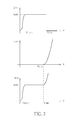
- FIGs. 2 and 3 are diagrams illustrating the operation of the slave driving stages ST 1 ⁇ ST N .
- the 1 st slave driving stage ST 1 is used for illustrative purpose.
- the current controller CC 1 When 0 ⁇ V 1 ⁇ V DROP , the current controller CC 1 is not completely turned on, and the luminescent device LED 1 remains off. Under such circumstance, the current controller CC 1 operates as a voltage-controlled device in a linear mode in which the current I CC1 and the total current I SUM1 change with the voltage V 1 in a specific manner, while the current I LED1 remains zero.
- the current I CC1 When V 1 >V DROP , the current I CC1 reaches the maximum current setting I SET1 of the 1 st slave driving stage ST 1 , and the current controller CC 1 switches to a constant-current mode and functions as a current limiter. In the embodiment illustrated in FIG. 2 , the current I CC1 is clamped at the constant value I SET1 instead of changing with the voltage V 1 in the constant-current mode. In the embodiment illustrated in FIG. 3 when V DROP ⁇ V 1 ⁇ V CUT , the luminescent device LED 1 remains off and the current controller CC 1 is configured to clamp the current I CC1 at the constant value I SET1 . In the embodiment illustrated in FIG.
- the current controller CC 1 may decrease the current I CC1 so that the total current I SUM1 flowing through the 1 st slave driving stage may be maintained at the constant value I SET1 instead of changing with the voltage V 1 in the constant-current mode.
- the current controller CC 1 switches to a cut-off mode.
- the current controller CC 1 functions as an open-circuited device, allowing the current I LED1 and the current I SUM1 to increase with the voltage V 1 .
- each of the current controller in the slave driving stages ST 1 ⁇ ST N is configured to operate in two phases.
- the slave driving stages ST 1 ⁇ ST N provide respective current settings I SET1 ⁇ I SETN , and the current I SUM1 ⁇ I SUMN mainly flow through the corresponding current controllers CC 1 ⁇ CC N .
- the current controllers CC 1 ⁇ CC N are turned off, and the current I SUM1 ⁇ I SUMN totally flow through the corresponding luminescent devices LED 1 ⁇ LED N .
- Each of the slave driving stages ST 1 ⁇ ST N may adopt any device configured to achieve the above-mentioned two-phase operations, such as the I-V curves depicted in FIGs. 2 and 3 .
- the configuration of the slave driving stages ST 1 ⁇ ST N and the I-V characteristics depicted in FIGs. 2 and 3 do not limit the scope of the present invention.
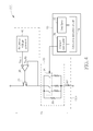
- FIGs. 4 ⁇ 6 are diagrams of the current control unit CCU in the master driving stage ST 0 according to embodiments of the present invention.
- the current control unit CCU including a current controller CC 0 and a current envelope controller 50, is configured to provide a current envelope I SET (t) with varying current settings.
- the current controller CC 0 includes a current detector 10, a switch 20, a comparator 30 and a reference voltage generator 40.
- the equivalent resistance R s (t) of the current detector 10 may be a constant value R S0 or varies according to the current envelope controller 50.
- the current detector 10 is configured to detect the current flowing through switch 20, thereby providing a corresponding feedback voltage V FB (t), which may be a constant value V FB0 or varies with time according to the current envelope controller 50.
- the switch 20 may include a field effect transistor (FET), a bipolar junction transistor (BJT) or other devices having similar function. In FIGs.
- N-MOSFET N-channel metal-oxide-semiconductor field effect transistor
- the reference voltage generator 40 is configured to provide a reference voltage V REF (t) which may be a constant value V REF0 or varies with time according to the current envelope controller 50.
- the comparator 30 includes a positive input end coupled to the reference voltage V REF (t), a negative input end coupled to the feedback voltage V FB (t), and an output end coupled to the control end of the switch 20.
- the comparator 30 is configured to adjust the current flowing through the switch 20 according to the relationship between the reference voltage V REF (t) and the feedback voltage V FB (t).
- V FB (t) ⁇ V REF (t) the comparator 30 is configured to raise its output voltage for increasing the current flowing through the switch 20 until the feedback voltage V FB (t) reaches the reference voltage V REF (t).
- V FB (t)>V REF (t) the comparator 30 is configured to decrease its output voltage for reducing the current flowing through the switch 20 until the feedback voltage V FE (t) reaches the reference voltage V REF (t).
- the current setting of the current envelope I SET (t) is equal to (V REF (t)/R s (t)) at a specific time t during a cycle of the rectified voltage V AC .
- the current envelope controller 50 includes an oscillator 52, a zero-cross detection circuit 54 and a control logic unit 56.
- the oscillator 52 is configured to provide internal clock signals based on which the current envelope controller 50 operates.
- the zero-cross detection circuit 54 is configured to detect the rising edge and falling edges of the current I LED , thereby determining the zero-cross points of the rectified AC voltage V AC .
- the control logic unit 56 is configured to adjust the values of V REF (t) and/or R s (t) of the current controller CC 0 for setting the levels of the current envelope I SET (t).
- the current detector 10 may include a plurality of resistors and a switching unit 15.
- the switching unit 15 includes a plurality of switches, each of which is turned on or off according to the current envelope controller 50 for adjusting the equivalent resistance R s (t) of the current detector 10.
- R S0 the equivalent resistance of the current detector 10
- the reference voltage generator 40 may include a plurality of resistors and a switching unit 45 forming an adjustable voltage-dividing circuit.
- the switching unit 45 includes a plurality of switches, each of which is turned on or off according to the current envelope controller 50 for adjusting the ratio of voltage division.
- the current detector 10 may include a plurality of resistors and a switching unit 15.
- the switching unit 15 includes a plurality of switches, each of which is turned on or off according to the current envelope controller 50 for adjusting the equivalent resistance R S (t) of the current detector 10.
- the voltage generator 40 may include a plurality of resistors and a switching unit 45 forming an adjustable voltage-dividing circuit.
- the switching unit 45 includes a plurality of switches, each of which is turned on or off according to the current envelope controller 50 for adjusting the ratio of voltage division.
- the equivalent resistance of the current detector 10 is equal to R S0
- the voltage generator 40 outputs a constant reference voltage V REF0
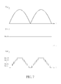
- FIG. 7 is a diagram illustrating the operation of the current control unit CCU in the master driving stage ST 0 according to an embodiment of the present invention.
- the current control unit CCU When the current envelope controller 50 is deactivated, the current control unit CCU is configured to provide the current envelope I SET (t) with a constant current setting I MAX0 which does not vary with the rectified AC voltage V AC , as depicted in the middle of FIG. 7 .
- the current control unit CCU is configured to provide the current envelope I SET (t) with various current settings whose value ranges between I MAXO ⁇ I MAXN , as depicted at the bottom of FIG. 7 .
- the current settings of the current controllers CC 0 ⁇ CC N have the following relationship: I MAX0 >I SETN >I MAXN >...>I SET2 >I MAX2 >I SET1 >I MAX1 .
- FIGs. 8-11 are diagrams illustrating the operation of the LED lighting device 100.
- the current controllers CC 0 in the master driving stage ST 0 provides the current envelope I SET (t) with 3 current settings I MAXO ⁇ I MAX2 , wherein I MAX0 >I SET2 >I MAX2 >I SET1 >I MAX1 .
- the LED lighting device 100 is driven by the rectified AC voltage V AC at its upper bound, which may be due to a decrease in load voltage or an increase in the AC voltage VS.
- the LED lighting device 100 is driven by the rectified AC voltage V AC at its lower bound, which may be due to an increase in load voltage or a decrease in the AC voltage VS.
- the rectified AC voltage V AC at its upper bound results in a higher power factor than at its lower bound.
- I LED ' represents the overall current of the LED lighting device 100 when the current envelope controller 50 is deactivated.
- the current controller CC 1 is configured to provide a constant current setting I SET1 when operating in the ON phase.
- the current controller CC 2 is configured to provide a constant current setting I SET2 when operating in the ON phase.
- the current controller CC 0 is configured to provide a current envelope with a constant current setting I MAX0 when operating in the ON phase, as depicted in the middle of FIG. 7 .
- the overall current I LED ' of the LED lighting device 100 is regulated by an active current controller (in ON phase) which provides the lowest current setting.
- t 0 ⁇ t 11 represent different time points during a cycle of the rectified AC voltage V AC .
- Table. 1 t 0 t 1 t 2 t 3 t 4 t 5 t 6 t 7 t 8 t 9 t 10 t 11 CC 1 ON OFF ON CC 2 ON ON OFF ON ON CC 0 ON (I MAX0 ) I LED ' I SET1 I SET2 I MAX0 I SET2 I SET1
- the current controllers CC 1 , CC 2 and CC 0 are turned on.
- the current I LED is regulated by the active current controllers CC 1 with the lowest current setting I SET1 (I SET1 ⁇ I SET2 ).
- the current controllers CC 2 and CC 0 are turned on, and the current controller CC 1 is turned off.
- the current I LED ' is regulated by the active current controllers CC 2 with the lowest current setting I SET2 (I SET2 ⁇ I MAX0 ).
- the current controller CC 0 is turned on, and the current controllers CC 1 and CC 2 are turned off.
- the current I LED ' is regulated by the only active current controller CC 0 with the current setting I MAX0 .
- the current controllers CC 1 , CC2 and CC 0 are turned on.
- the current I LED ' is regulated by the active current controllers CC 1 with the lowest current setting I SET1 (I SET1 ⁇ I MAX0 ).
- the current controllers CC 2 and CC 0 are turned on, and the current controller CC 1 is turned off.
- the current I LED ' is regulated by the active current controllers CC 2 with the lowest current setting I SET2 (I SET2 ⁇ I MAX0 ).
- the current controller CC 0 is turned on, and the current controllers CC 1 and CC 2 are turned off.
- the current I LED ' is regulated by the only active current controller CC 0 with the current setting I MAX0 .
- I LED represents the overall current of the LED lighting device 100 when the current envelope controller 50 is activated.
- the current controller CC 1 is configured to provide a constant current setting I SET1 when operating in the ON phase.
- the current controller CC 2 is configured to provide a constant current setting I SET2 when operating in the ON phase.
- the current controller CC 0 is configured to provide a current envelope I SET (t) with various current settings ranging between I MAX0 ⁇ I MAX2 , as depicted at the bottom of FIG. 7 .
- the overall current I LED of the LED lighting device 100 is regulated by an active current controller which provides the lowest current setting.
- the current controllers CC 1 , CC2 and CC 0 are turned on.
- the current I LED is regulated by the active current controllers CC 0 with the lowest current setting I MAX1 (I MAX1 ⁇ I SET1 ).
- I MAX1 I MAX1 ⁇ I SET1
- the current controllers CC 2 and CC 0 are turned on, and the current controller CC 1 is turned off.
- the current I LED is regulated by the active current controllers CC 0 with the lowest current setting I MAX1 (I MAX1 ⁇ I SET2 ) between t 2 ⁇ t 3 and t 8 ⁇ t 9 , and by the active current controllers CC 0 with the current setting I MAX2 (I MAX2 ⁇ I SET2 ) between t 3 ⁇ t 4 and t 7 ⁇ t 8 . Between t 4 ⁇ t 7 , the current controller CC 0 is turned on, and the current controllers CC 1 and CC 2 are turned off. The current I LED is regulated by the only active current controller CC 0 with the current setting I MAX2 between t 4 ⁇ t 5 and t 6 ⁇ t 7 , and with the current setting I MAX0 between t 5 ⁇ t 6 .
- the current controllers CC 1 , CC2 and CC0 are turned on, and the current controller CC2 is turned off.
- the current ILED is regulated by the active current controllers CC0 with the lowest current setting IMAX1 (IMAX ⁇ ISET1) between s0-s2 and s9 ⁇ s11, and by the active current controllers CC 1 with the lowest current setting ISET1 (ISET1 ⁇ IMAX2) between s2 ⁇ s3 and s8 ⁇ s9.
- IMAX ⁇ ISET1 IMAX ⁇ ISET1
- ISET1 ⁇ IMAX2 and CC0 are turned on, and the current controller CC1 is turned off.
- the current ILED is regulated by the active current controllers CC 0 with the lowest current setting IMAX2 (IMAX2 ⁇ ISET2) between s3 ⁇ s4 and s7 ⁇ s8, and by the active current controllers CC2 with the lowest current setting ISET2 (ISET2 ⁇ IMAX0) between s4 ⁇ s5 and s6 ⁇ s7. Between s5 ⁇ s6, the current controller CC0 is turned on, and the current controllers CC1 and CC2 are turned off. The current ILED is regulated by the only active current controller CC0 with the current setting IMAX0.
- the current ILED' when the LED lighting device 100 is driven by the rectified AC voltage VAC at its upper bound, the current ILED' (with the current envelope controller 50 deactivated) reaches IMAX earlier and drops below IMAX later than the current ILED (with the current envelope controller 50 activated), resulting in a wider waveform which indicates a duty increase.
- the current ILED' when the LED lighting device 100 is driven by the rectified AC voltage VAC at its lower bound, the current ILED' (with the current envelope controller 50 deactivated) reaches IMAX later and drops below IMAX earlier than the current ILED (with the current envelope controller 50 activated), resulting in a narrower waveform which indicates a duty decrease.
- the duty increase due to larger VAC and the duty decrease due to smaller VAC may greatly degrade the line regulation of the LED lighting device 100.
- the present invention may improve the line/load regulation of the LED lighting device 100 by activating the current envelope controller 50 of the current control unit CCU in the master driving stage ST0. Even if the rectified AC voltage VAC somehow fluctuates between its upper bound and lower bound, the current envelope controller 50 is able to reduce the duty variation.
- the present invention may improve the effective operational voltage range and line/load regulation of an LED lighting device.
Landscapes
- Circuit Arrangement For Electric Light Sources In General (AREA)
Applications Claiming Priority (1)
| Application Number | Priority Date | Filing Date | Title |
|---|---|---|---|
| US14/277,029 US9226354B2 (en) | 2013-06-03 | 2014-05-13 | Light-emitting diode lighting device having multiple driving stages |
Publications (2)
| Publication Number | Publication Date |
|---|---|
| EP2945466A2 true EP2945466A2 (de) | 2015-11-18 |
| EP2945466A3 EP2945466A3 (de) | 2016-07-20 |
Family
ID=53180571
Family Applications (1)
| Application Number | Title | Priority Date | Filing Date |
|---|---|---|---|
| EP15167698.8A Ceased EP2945466A3 (de) | 2014-05-13 | 2015-05-13 | Leuchtdiodenbeleuchtungsvorrichtung mit mehreren ansteuerungsstufen |
Country Status (1)
| Country | Link |
|---|---|
| EP (1) | EP2945466A3 (de) |
Cited By (2)
| Publication number | Priority date | Publication date | Assignee | Title |
|---|---|---|---|---|
| CN113939063A (zh) * | 2021-12-17 | 2022-01-14 | 深圳市明微电子股份有限公司 | Led系统供电电源控制方法及供电电源可控的led系统 |
| AT17629U1 (de) * | 2017-04-20 | 2022-09-15 | Zumtobel Lighting Gmbh | Schaltungsanordnung zum Betreiben von Leuchtmitteln |
Family Cites Families (4)
| Publication number | Priority date | Publication date | Assignee | Title |
|---|---|---|---|---|
| US8102683B2 (en) * | 2010-02-09 | 2012-01-24 | Power Integrations, Inc. | Phase angle measurement of a dimming circuit for a switching power supply |
| US8638047B2 (en) * | 2010-12-07 | 2014-01-28 | Iml International | Two-terminal current controller and related LED lighting device |
| US9516718B2 (en) * | 2011-12-29 | 2016-12-06 | Seoul Semiconductor Co., Ltd. | LED luminescence apparatus |
| KR20130110410A (ko) * | 2012-03-29 | 2013-10-10 | 엘지전자 주식회사 | 전력 보상 기능을 갖는 발광 다이오드 조명 장치 |
-
2015
- 2015-05-13 EP EP15167698.8A patent/EP2945466A3/de not_active Ceased
Non-Patent Citations (1)
| Title |
|---|
| None |
Cited By (3)
| Publication number | Priority date | Publication date | Assignee | Title |
|---|---|---|---|---|
| AT17629U1 (de) * | 2017-04-20 | 2022-09-15 | Zumtobel Lighting Gmbh | Schaltungsanordnung zum Betreiben von Leuchtmitteln |
| CN113939063A (zh) * | 2021-12-17 | 2022-01-14 | 深圳市明微电子股份有限公司 | Led系统供电电源控制方法及供电电源可控的led系统 |
| CN113939063B (zh) * | 2021-12-17 | 2022-03-22 | 深圳市明微电子股份有限公司 | Led系统供电电源控制方法及供电电源可控的led系统 |
Also Published As
| Publication number | Publication date |
|---|---|
| EP2945466A3 (de) | 2016-07-20 |
Similar Documents
| Publication | Publication Date | Title |
|---|---|---|
| US8638043B2 (en) | Two-terminal current controller and related LED lighting device | |
| US9414452B1 (en) | Light-emitting diode lighting device with synchronized PWM dimming control | |
| US8319443B2 (en) | Two-terminal current controller and related LED lighting device | |
| US8638047B2 (en) | Two-terminal current controller and related LED lighting device | |
| EP2326145A1 (de) | LED-Lampe und LED-Lampenmodul | |
| KR101683438B1 (ko) | 조명 시스템 및 그의 제어 회로 | |
| US20110163684A1 (en) | Driving circuit of light emitting diode and lighting apparatus using the same | |
| US9013109B2 (en) | Light-emitting diode lighting device with adjustable current settings and switch voltages | |
| TWI519204B (zh) | 具備多級驅動階段之發光二極體照明裝置 | |
| US9265102B2 (en) | Light-emitting diode lighting device with adjustable color rendering indexes | |
| TWI547201B (zh) | 具備多級驅動階段之發光二極體照明裝置 | |
| KR101681481B1 (ko) | 복수의 구동 스테이지를 갖는 로-플리커 발광 다이오드 조명 장치 | |
| US11224103B2 (en) | LED lighting apparatus | |
| US9226354B2 (en) | Light-emitting diode lighting device having multiple driving stages | |
| KR20160094020A (ko) | 발광 다이오드 조명 장치의 제어 회로 및 제어 방법 | |
| KR101408027B1 (ko) | 2-단자 전류 제어기 및 관련 led 조명 장치 | |
| US8890433B2 (en) | Two-terminal current controller and related LED lighting device | |
| US8674609B2 (en) | Two-terminal current controller and related LED lighting device | |
| EP2941098A2 (de) | Leuchtdiodenbeleuchtungsvorrichtung mit mehreren ansteuerungsstufen |
Legal Events
| Date | Code | Title | Description |
|---|---|---|---|
| PUAI | Public reference made under article 153(3) epc to a published international application that has entered the european phase |
Free format text: ORIGINAL CODE: 0009012 |
|
| AK | Designated contracting states |
Kind code of ref document: A2 Designated state(s): AL AT BE BG CH CY CZ DE DK EE ES FI FR GB GR HR HU IE IS IT LI LT LU LV MC MK MT NL NO PL PT RO RS SE SI SK SM TR |
|
| AX | Request for extension of the european patent |
Extension state: BA ME |
|
| PUAL | Search report despatched |
Free format text: ORIGINAL CODE: 0009013 |
|
| AK | Designated contracting states |
Kind code of ref document: A3 Designated state(s): AL AT BE BG CH CY CZ DE DK EE ES FI FR GB GR HR HU IE IS IT LI LT LU LV MC MK MT NL NO PL PT RO RS SE SI SK SM TR |
|
| AX | Request for extension of the european patent |
Extension state: BA ME |
|
| RIC1 | Information provided on ipc code assigned before grant |
Ipc: H05B 33/08 20060101AFI20160616BHEP |
|
| STAA | Information on the status of an ep patent application or granted ep patent |
Free format text: STATUS: REQUEST FOR EXAMINATION WAS MADE |
|
| 17P | Request for examination filed |
Effective date: 20170119 |
|
| RBV | Designated contracting states (corrected) |
Designated state(s): AL AT BE BG CH CY CZ DE DK EE ES FI FR GB GR HR HU IE IS IT LI LT LU LV MC MK MT NL NO PL PT RO RS SE SI SK SM TR |
|
| STAA | Information on the status of an ep patent application or granted ep patent |
Free format text: STATUS: EXAMINATION IS IN PROGRESS |
|
| 17Q | First examination report despatched |
Effective date: 20200609 |
|
| RAP1 | Party data changed (applicant data changed or rights of an application transferred) |
Owner name: IML HONGKONG LIMITED |
|
| STAA | Information on the status of an ep patent application or granted ep patent |
Free format text: STATUS: THE APPLICATION HAS BEEN REFUSED |
|
| 18R | Application refused |
Effective date: 20220401 |