EP2952963B1 - Procédé pour calculer les paramètres d'un procédé de fabrication de circuits intégrés - Google Patents
Procédé pour calculer les paramètres d'un procédé de fabrication de circuits intégrés Download PDFInfo
- Publication number
- EP2952963B1 EP2952963B1 EP14305834.5A EP14305834A EP2952963B1 EP 2952963 B1 EP2952963 B1 EP 2952963B1 EP 14305834 A EP14305834 A EP 14305834A EP 2952963 B1 EP2952963 B1 EP 2952963B1
- Authority
- EP
- European Patent Office
- Prior art keywords
- function
- interest
- point
- target design
- kernel
- Prior art date
- Legal status (The legal status is an assumption and is not a legal conclusion. Google has not performed a legal analysis and makes no representation as to the accuracy of the status listed.)
- Active
Links
Images


Classifications
-
- G—PHYSICS
- G03—PHOTOGRAPHY; CINEMATOGRAPHY; ANALOGOUS TECHNIQUES USING WAVES OTHER THAN OPTICAL WAVES; ELECTROGRAPHY; HOLOGRAPHY
- G03F—PHOTOMECHANICAL PRODUCTION OF TEXTURED OR PATTERNED SURFACES, e.g. FOR PRINTING, FOR PROCESSING OF SEMICONDUCTOR DEVICES; MATERIALS THEREFOR; ORIGINALS THEREFOR; APPARATUS SPECIALLY ADAPTED THEREFOR
- G03F7/00—Photomechanical, e.g. photolithographic, production of textured or patterned surfaces, e.g. printing surfaces; Materials therefor, e.g. comprising photoresists; Apparatus specially adapted therefor
- G03F7/70—Microphotolithographic exposure; Apparatus therefor
- G03F7/70483—Information management; Active and passive control; Testing; Wafer monitoring, e.g. pattern monitoring
- G03F7/70491—Information management, e.g. software; Active and passive control, e.g. details of controlling exposure processes or exposure tool monitoring processes
- G03F7/705—Modelling or simulating from physical phenomena up to complete wafer processes or whole workflow in wafer productions
-
- G—PHYSICS
- G03—PHOTOGRAPHY; CINEMATOGRAPHY; ANALOGOUS TECHNIQUES USING WAVES OTHER THAN OPTICAL WAVES; ELECTROGRAPHY; HOLOGRAPHY
- G03F—PHOTOMECHANICAL PRODUCTION OF TEXTURED OR PATTERNED SURFACES, e.g. FOR PRINTING, FOR PROCESSING OF SEMICONDUCTOR DEVICES; MATERIALS THEREFOR; ORIGINALS THEREFOR; APPARATUS SPECIALLY ADAPTED THEREFOR
- G03F1/00—Originals for photomechanical production of textured or patterned surfaces, e.g., masks, photo-masks, reticles; Mask blanks or pellicles therefor; Containers specially adapted therefor; Preparation thereof
- G03F1/36—Masks having proximity correction features; Preparation thereof, e.g. optical proximity correction [OPC] design processes
-
- G—PHYSICS
- G03—PHOTOGRAPHY; CINEMATOGRAPHY; ANALOGOUS TECHNIQUES USING WAVES OTHER THAN OPTICAL WAVES; ELECTROGRAPHY; HOLOGRAPHY
- G03F—PHOTOMECHANICAL PRODUCTION OF TEXTURED OR PATTERNED SURFACES, e.g. FOR PRINTING, FOR PROCESSING OF SEMICONDUCTOR DEVICES; MATERIALS THEREFOR; ORIGINALS THEREFOR; APPARATUS SPECIALLY ADAPTED THEREFOR
- G03F1/00—Originals for photomechanical production of textured or patterned surfaces, e.g., masks, photo-masks, reticles; Mask blanks or pellicles therefor; Containers specially adapted therefor; Preparation thereof
- G03F1/68—Preparation processes not covered by groups G03F1/20 - G03F1/50
- G03F1/80—Etching
-
- G—PHYSICS
- G03—PHOTOGRAPHY; CINEMATOGRAPHY; ANALOGOUS TECHNIQUES USING WAVES OTHER THAN OPTICAL WAVES; ELECTROGRAPHY; HOLOGRAPHY
- G03F—PHOTOMECHANICAL PRODUCTION OF TEXTURED OR PATTERNED SURFACES, e.g. FOR PRINTING, FOR PROCESSING OF SEMICONDUCTOR DEVICES; MATERIALS THEREFOR; ORIGINALS THEREFOR; APPARATUS SPECIALLY ADAPTED THEREFOR
- G03F7/00—Photomechanical, e.g. photolithographic, production of textured or patterned surfaces, e.g. printing surfaces; Materials therefor, e.g. comprising photoresists; Apparatus specially adapted therefor
- G03F7/70—Microphotolithographic exposure; Apparatus therefor
- G03F7/70425—Imaging strategies, e.g. for increasing throughput or resolution, printing product fields larger than the image field or compensating lithography- or non-lithography errors, e.g. proximity correction, mix-and-match, stitching or double patterning
- G03F7/70433—Layout for increasing efficiency or for compensating imaging errors, e.g. layout of exposure fields for reducing focus errors; Use of mask features for increasing efficiency or for compensating imaging errors
- G03F7/70441—Optical proximity correction [OPC]
-
- G—PHYSICS
- G06—COMPUTING OR CALCULATING; COUNTING
- G06F—ELECTRIC DIGITAL DATA PROCESSING
- G06F30/00—Computer-aided design [CAD]
- G06F30/30—Circuit design
- G06F30/39—Circuit design at the physical level
- G06F30/398—Design verification or optimisation, e.g. using design rule check [DRC], layout versus schematics [LVS] or finite element methods [FEM]
-
- H—ELECTRICITY
- H01—ELECTRIC ELEMENTS
- H01J—ELECTRIC DISCHARGE TUBES OR DISCHARGE LAMPS
- H01J37/00—Discharge tubes with provision for introducing objects or material to be exposed to the discharge, e.g. for the purpose of examination or processing thereof
- H01J37/30—Electron-beam or ion-beam tubes for localised treatment of objects
- H01J37/317—Electron-beam or ion-beam tubes for localised treatment of objects for changing properties of the objects or for applying thin layers thereon, e.g. for ion implantation
- H01J37/3174—Particle-beam lithography, e.g. electron beam lithography
-
- H—ELECTRICITY
- H01—ELECTRIC ELEMENTS
- H01J—ELECTRIC DISCHARGE TUBES OR DISCHARGE LAMPS
- H01J37/00—Discharge tubes with provision for introducing objects or material to be exposed to the discharge, e.g. for the purpose of examination or processing thereof
- H01J37/30—Electron-beam or ion-beam tubes for localised treatment of objects
- H01J37/317—Electron-beam or ion-beam tubes for localised treatment of objects for changing properties of the objects or for applying thin layers thereon, e.g. for ion implantation
- H01J37/3178—Electron-beam or ion-beam tubes for localised treatment of objects for changing properties of the objects or for applying thin layers thereon, e.g. for ion implantation for applying thin layers on objects
-
- G—PHYSICS
- G06—COMPUTING OR CALCULATING; COUNTING
- G06F—ELECTRIC DIGITAL DATA PROCESSING
- G06F2119/00—Details relating to the type or aim of the analysis or the optimisation
- G06F2119/18—Manufacturability analysis or optimisation for manufacturability
-
- Y—GENERAL TAGGING OF NEW TECHNOLOGICAL DEVELOPMENTS; GENERAL TAGGING OF CROSS-SECTIONAL TECHNOLOGIES SPANNING OVER SEVERAL SECTIONS OF THE IPC; TECHNICAL SUBJECTS COVERED BY FORMER USPC CROSS-REFERENCE ART COLLECTIONS [XRACs] AND DIGESTS
- Y02—TECHNOLOGIES OR APPLICATIONS FOR MITIGATION OR ADAPTATION AGAINST CLIMATE CHANGE
- Y02P—CLIMATE CHANGE MITIGATION TECHNOLOGIES IN THE PRODUCTION OR PROCESSING OF GOODS
- Y02P90/00—Enabling technologies with a potential contribution to greenhouse gas [GHG] emissions mitigation
- Y02P90/02—Total factory control, e.g. smart factories, flexible manufacturing systems [FMS] or integrated manufacturing systems [IMS]
Definitions
- the present invention notably applies to the field of electronic or optical lithography. It applies, among other processes, to mask write and direct write. It can also apply to other steps of semiconductor manufacturing processes, such as nanoimprint, DSA (Directed Self Assembly), etching, CMP (Chemical Mechanical Polishing/Planarization), annealing, baking, metrology, etc...
- Tools that can be used to calculate representative variables in the residual models are the visibility kernels, such as those disclosed by Sato ( S. Sato, K. Ozawa, and F. Uesawa, "Dry-etch proximity function for model-based OPC beyond 65-nm node", proc. SPIE vol 6155, 2006 ), or Park ( J.-G. Park, S.-W. Kim, S.-B. Shim, S.-S. Suh, and H.-K. Oh, "The effective etch process proximity correction methodology for improving on chip CD variation in 20 nm node DRAM gate', Design for Manufacturability though Design-Process Integration V, proc. SPIE vol 7974, 2011 ). Also, US patent applications published under n° US2010/269084 , US2011/138343 , US2012/221982 and US2006/075378 disclose visibility kernels to scan semiconductor designs.
- the invention solves this problem and alleviates the computing workload by calculating the metrics of the model by products of convolution of the target design and a new type of method wherein a kernel function is oriented by a deformation function using a shift angle and the characteristics of the design of the integrated circuit to be manufactured are calculated using a convolution across the whole design.
- the invention discloses A method of determining, by a computer, at least a component of a vector representing a metric of a process for manufacturing a semiconductor integrated circuit defined by a target design, said method being characterized in that it comprises: selecting at least a point of the target design as a point of interest (x, y); selecting a kernel function K(r) centered on the at least a point of interest, said kernel function depending on a radius; calculating over the target design at least a convolution of the target design and a compound of the kernel function K(r) and a deformation function f x,y ( ⁇ , ⁇ x,y ), said deformation function depending on the angle of interest and a selected shift angle ⁇ x,y ; determining a value of the at least a component V(x,y) from the value of the convolution function at the at least a point of interest (x,y).
- the at least a component is an external density of the target design at the point of interest, which is determined from a convolution function where the shift angle ⁇ x,y is selected to scan outside parts of the design from the point of interest.
- the at least a component is an internal density of the target design at the point of interest, which is determined from a convolution function where the shift angle ⁇ x,y ' is selected to scan inside parts of the design from the point of interest.
- the shift angle ⁇ x,y ' is equal to ⁇ x,y + ⁇
- the kernel function is an isotropic function.
- the kernel function is a Gaussian function.
- the deformation function is a compound of trigonometric functions selected to be null for values of the angle of interest higher than ⁇ .
- the deformation function is a compound of one of squares and cubic powers of trigonometric functions selected to be null for values of the angle of interest higher than ⁇ .
- the deformation function is replaced by a Fourier series development.
- the Fourier series development is developed at a n th order, n being selected so that the product of convolution developed at the n th order is invariant across rotations around the point of interest, within a tolerance of the corrections to be applied to the target design.
- the deformation function is replaced by a projection of a couple of basic kernel functions, said basic kernel functions with angular variations selected to scan the domain of variation of the shift angle ⁇ x,y across the target design.
- the couple of basic kernel functions is selected so that the two selected basic kernel functions have angular variations which are above and under shift angle ⁇ x,y .
- the invention also discloses a computer program for determining at least a component of a vector representing a metric of a process for manufacturing a semiconductor integrated circuit defined by a target design, said computer program being characterized in that it comprises: computer code for selecting at least a point of the target design as a point of interest; computer code for selecting a kernel function centered on the at least a point of interest, said kernel function depending on a radius; computer code for calculating over the target design at least a convolution function of the target design and a compound of the kernel function and a deformation function, said deformation function depending on the angle of visibility and a selected shift angle; computer code for determining a value of the at least a component from the value of the convolution function at the at least a point of interest.
- the invention also discloses a semiconductor manufacturing equipment comprising a computer configured to run a computer program according to claim 13 and to use at least an output of a computer program according to the invention, said semiconductor manufacturing equipment configured for one of direct writing on semiconductor wafers, writing on a mask plate, etching, chemically or mechanically planarizing, or baking, annealing a semiconductor wafer, and inspecting a mask or semiconductor surface.
- Another advantage of the invention is that a calculation of the product of convolution can still be quickened by using, instead of the deformation function, its development in Fourier series at an adequate order.
- a decomposition of the product of convolution using a projection on an angular basis can also improve the speed of calculation.
- the use of a product of convolution allows a very effective factorization which again alleviates the computing workload.
- the use of a shift angle is specifically advantageous in the case of free-form designs, for which the use of surface integrals is quasi impossible. In this case, simple rules can be used to adapt the optimal shift angle when going along the contour of a design to model.
- Figures 1a, 1b and 1c represent an isotropic kernel function, and its implementation to define an external visible surface and an internal visible surface, in a method of the prior art.
- Figure 1a illustrates an isotropic area of interest 110a, which has a radius R.
- Figure 1b illustrates an intersection 130b of the area of visibility 110a from a point of interest 120b with a set of target patterns 140b. This intersection is external to the set of target patterns and can be used, as explained below to define the Space variable as the ratio of the surface of the intersection 130b to the surface of the area of visibility 110a.
- Figure 1c illustrates an intersection 130c of the area of visibility 110a from a point of interest 120b with a set of target patterns 140b. This intersection is internal to the set of target patterns and can be used, as explained below to define the CD variable as the ratio of the surface of the intersection 130c to the surface of the area of visibility 110a.
- T(r, ⁇ ) is null inside the plain parts of the layout and non-zero elsewhere.
- T(r, ⁇ ) is null outside the plain parts of the layout and non-zero elsewhere.
- the domain of integration is the surface which is visible from the point of interest. It is therefore to be noted that the limits of the domain of integration vary with each piece of the layout (i.e. with each point of interest) and that the procedure has to be repeated for all the points of interest (there may be as many as a few billions, in the case of complex layouts).
- Figures 2a, 2b and 2c represent an anisotropic kernel function, and its implementation to define an external visible surface and an internal visible surface, in another method of the prior art.
- Figure 2a illustrates an anisotropic area of simulation 210a, which has a radius R, and a deformation angle ⁇ .
- Figure 2b illustrates an intersection 230b of the area of interest 210a from a point of interest 220b with a set of target patterns 240b. This intersection is external to the set of target patterns and can be used, as explained below to define the Space variable as the ratio of the surface of the intersection 230b to the surface of the area of interest 210a. .
- Figure 2c illustrates an intersection 230c of the area of interest 210a from a point of interest 220b with a set of target patterns 240b. This intersection is internal to the set of target patterns and can be used, as explained below to define the CD variable as the ratio of the surface of the intersection 230c to the surface of the area of interest 210a.
- T(r, ⁇ ) is null inside the plain parts of the layout and non-zero elsewhere.
- T(r, ⁇ ) is null outside the plain parts of the layout and non-zero elsewhere.
- the domain of integration is the surface which is visible from the point of interest.
- This method has the advantage over the method of figures 1a, 1b and 1c to increase the accuracy of the representation of the target design, thanks to the deformation function A( ⁇ ). This is because it better takes into account the anisotropy, which characterizes most of IC manufacturing processes (which are not only shape dependent, but also direction dependent. But, It also suffers from the same disadvantages: the limits of the domain of integration vary with each piece of the layout (i.e. with each point of interest) and that the procedure has to be repeated for all the points of interest, which may mean billions, in the case of complex layouts.
- the invention corrects the disadvantages of these methods of the prior art.
- Figures 3a , 3b and 3c represent an oriented kernel, an external density function and an internal density function, in a number of embodiments of the invention.
- Figure 3a illustrates an anisotropic area of interest 310a, which has a radius R, and a deformation angle ⁇ .
- Figure 3b illustrates an intersection 330b of the area under computation 310a from a point of interest 320b with a set of target patterns 340b.
- the computation extends across the whole area under computation, even though some areas are not visible from the point of interest.
- the result of the computation is used, as explained below to define an External Density.
- the computation extends across the whole area under computation, even though some areas are not visible from the point of interest.
- the result of the computation is used, as explained below to define an Internal Density.
- the External Density and the Internal Density are computed as a convolution denoted by *, across the whole target design.
- V(x,y) a product of convolution V(x,y) of the target design, represented by a function L ( x,y ) with an oriented kernel N(x,y) as:
- V x y L x y ⁇ N x y
- N(u,v) the oriented kernel N(u,v)
- N(u,v) can be split into two contributions:
- N u v K u 2 + v 2 ⁇ f a tan v / u + ⁇
- K u 2 + v 2 is the Gaussian kernel function
- f ( a tan( v / u ) + ⁇ ) is a deformation function.
- the ⁇ angle is the shift angle of the deformation function which varies according to the location (x,y) on the design.
- the ⁇ angle has as reference, the axis for which the basis deformation function reaches its maximum.
- the shift angle may vary in the range [0, 2 ⁇ ]. Notice that ⁇ angle has only one possible value for (x,y) location. Thus, it can be considered as constant parameter for each V(x,y) calculation.
- f ( ⁇ + ⁇ ) is configured so that the kernel is oriented towards the outside of the pattern. Indeed if ⁇ is replaced by ⁇ + ⁇ , the Internal Density can be computed in parallel with External Density without further cost of calculation.
- f ( ⁇ + ⁇ ) is configured so that the kernel is oriented towards the inside of the design. Indeed if ⁇ is replaced by ⁇ + ⁇ , the External Density can be computed in parallel with Internal Density without further cost of calculation.
- the shift angle ⁇ is selected as the angle of view from the point of interest to the vertical axis on the design which maximizes the sensitivity of the product of convolution to the estimated metrics (Space or CD).
- the adequate shift angle will be ⁇ /2 (3 ⁇ /2) or 3 ⁇ /2 ( ⁇ /2), when the point of interest is on the right (left) edge of a vertical line and the observation is respectively to the outside or the inside of the design.
- the adequate shift angle will be ⁇ (zero) or zero ( ⁇ ), when the observation is respectively to the outside or the inside of the design.
- a preferred rule is that the shift angle ⁇ of the deformation function is selected as being optimal for the area of the patterned design (Manhattan or free-form, for instance).
- ⁇ is defined as the angle of the normal to the edge to the direction of reference.
- the shift angle can be defined as the angle between the bisectrix of the external angle of the two segments at the point of discontinuity and the direction of reference.
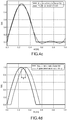
- Figures 4a, 4b , 4c and 4d respectively represent a deformation function, its Fourier series development at order 4, its Fourier series development at order 2 and a deformation function shifted by a specified angle, in a number of embodiments of the invention.
- Figure 4a illustrates the deformation function f ( ⁇ + ⁇ ), with a shift angle ⁇ equal to zero.
- f ( ⁇ + ⁇ ) can advantageously be a combination of truncated basic trigonometric functions.
- other functions, with different values for different intervals may be selected, or different powers, as a function of the target design and the specific process to be modeled. For instance, if more directivity than the one allowed by simple trigonometric functions is needed, square or cubic sine or cosine functions can be advantageously used..
- a n 1 ⁇ ⁇ 0 2 ⁇ f ⁇ + ⁇ . cos n ⁇ + n ⁇ d ⁇
- b n 1 ⁇ ⁇ 0 2 ⁇ f ⁇ + ⁇ . sin n ⁇ + n ⁇ d ⁇
- Figure 4c represents an approximation of the same deformation function by a Fourier series development at order 2.
- the figure demonstrates that, in the case of this example, an order 2 development can be quite accurate.
- the order of the development will be selected so that, over a number of representative patterned designs, the approximation remains invariant by rotation within the tolerance of the correction to be modeled. And of course, the lesser the order of the development, the more efficient the computation will be.
- Figure 4d illustrates an embodiment of the invention where the shift angle ⁇ is different from zero.
- the oriented metric V(x,y) is defined by Equation 1, with the same notations as defined above.
- dudv + ⁇ a n ⁇ sin n ⁇ + b n ⁇ cos n ⁇ ⁇ ⁇ ⁇ ⁇ ⁇ ⁇ ⁇ K x ⁇ u 2 + y ⁇ v 2 ⁇ sin n ⁇ a tan y ⁇ v / x ⁇ u ⁇ L u v . dudv )
- Equation 5 may be pre-calculated, stored in tables, and then used in the calculation of V(x,y) with the coefficients a n and b n of the Fourier series development and the trigonometric functions of ⁇ .
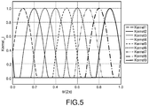
- Figure 5 illustrates a basis of 9 kernel functions used to project the product of convolution of the oriented kernel and a patterned design in a number of embodiments of the invention.
- the product of convolution is decomposed into nine basic kernel functions, which can be sine or cosine functions, or among others squares or cubic functions thereof, which are all defined by a different angle.
- the two basic kernels with angles on each side of the shift angle are used to compute the product of convolution by projection on the direction of reference of the patterned design.
- the figure is only illustrative of one embodiment among a plurality: for instance the number of kernels may be chosen as low as 3 or as high as a few tens, depending upon the precision which is required by the application.
- the method of the invention may be used in many use cases in the manufacturing process of semiconductor ICs. More specifically, it is well suited for certain types of e-beam lithography processes to replace a method wherein the proximity effect corrections are calculated through a simulation which is decomposed in a first step wherein a convolution between a Point Spread Function (PSF) and the design and a second step wherein the resist threshold is taken into account.
- PSF Point Spread Function
- a more precise resist model which can be adjusted to any type of process signature is very efficient. This is especially the case to model e-beam lithography processes after etching and/or when extreme ultra-violet (EUV) masks are used. This is because extreme UV are covered by an heavy metal layer (Tantalium or tantalium nitride) which creates significant back-scattering effects.
- EUV extreme ultra-violet
- the metrics of the invention can be used to calibrate a differential model as is disclosed by European patent application EP 2014 0 305 835 filed this same day assigned to one of the applicants, titled "Method for determining the parameters of an IC manufacturing process by a differential procedure".
Landscapes
- Physics & Mathematics (AREA)
- General Physics & Mathematics (AREA)
- Engineering & Computer Science (AREA)
- Computer Hardware Design (AREA)
- Theoretical Computer Science (AREA)
- Analytical Chemistry (AREA)
- Chemical & Material Sciences (AREA)
- General Engineering & Computer Science (AREA)
- Geometry (AREA)
- Evolutionary Computation (AREA)
- Exposure And Positioning Against Photoresist Photosensitive Materials (AREA)
- Exposure Of Semiconductors, Excluding Electron Or Ion Beam Exposure (AREA)
- Preparing Plates And Mask In Photomechanical Process (AREA)
- Electron Beam Exposure (AREA)
- Mechanical Treatment Of Semiconductor (AREA)
Claims (14)
- Procédé de détermination, par un ordinateur, d'au moins une composante d'un vecteur représentant une métrique d'un procédé pour la fabrication d'un circuit intégré à semi-conducteur défini par un modèle cible (340b), ledit procédé étant caractérisé en ce qu'il comprend :- la sélection d'au moins un point du modèle cible comme point d'intérêt (x,y), (320b) ;- la sélection d'une fonction noyau K(r) centrée sur le au moins un point d'intérêt, ladite fonction noyau dépendant du rayon ;- le calcul sur le modèle cible (320b) d'au moins une convolution du modèle cible et d'un composé de la fonction noyau K(r) et d'une fonction de déformation fx,y(θ,ϕx,y), ladite fonction de déformation dépendant de l'angle d'intérêt et d'un angle de décalage sélectionné ϕx,y ;- la détermination d'une valeur de l'au moins une composante V(x,y) à partir de la valeur de la fonction de convolution au niveau de l'au moins un point d'intérêt (x,y), (320b).
- Procédé selon la revendication 1, dans lequel la au moins une composante est une densité externe du modèle cible au niveau du point d'intérêt, qui est déterminée à partir d'une fonction de convolution où l'angle de décalage ϕx,y est sélectionné pour balayer des parties extérieures du modèle à partir du point d'intérêt.
- Procédé selon la revendication 1, dans lequel la au moins une composante est une densité interne du modèle cible au niveau du point d'intérêt, qui est déterminée à partir d'une fonction de convolution où l'angle de décalage ϕx,y' est sélectionné pour balayer des parties intérieures du modèle à partir du point d'intérêt.
- Procédé selon les revendications 2 et 3, dans lequel l'angle de décalage ϕx,y' est égal à ϕx,y + π.
- Procédé selon l'une quelconque des revendications 1 à 4, dans lequel la fonction noyau est une fonction isotrope.
- Procédé selon la revendication 5, dans lequel la fonction noyau est une fonction Gaussienne.
- Procédé selon l'une quelconque des revendications 1 à 6, dans lequel la fonction de déformation est un composé de fonctions trigonométriques sélectionné afin d'être nul pour des valeurs d'angle d'intérêt supérieures à π.
- Procédé selon l'une quelconque des revendications 1 à 6, dans lequel la fonction de déformation est un composé d'une de puissances carrées et cubes de fonctions trigonométriques sélectionné afin d'être nul pour des valeurs d'angle d'intérêt supérieures à π.
- Procédé selon l'une quelconque des revendications 1 à 8, dans lequel la fonction de déformation est remplacée par un développement de série de Fourier.
- Procédé selon la revendication 9, dans lequel le développement d'une série de Fourier est développé à un nième ordre, n étant sélectionné de sorte que le produit de convolution développé au nième ordre soit invariable à travers les rotations autour du point d'intérêt, dans une tolérance de corrections à appliquer au modèle cible.
- Procédé selon l'une quelconque des revendications 1 à 8, dans lequel la fonction de déformation est remplacée par une projection d'une paire de fonctions noyaux basiques, lesdites fonctions noyaux basiques présentant des variations angulaires étant sélectionnées pour balayer le domaine de variation de l'angle de décalage ϕx,y à travers le modèle cible.
- Procédé selon la revendication 11, dans lequel la paire de fonctions noyaux basiques est sélectionnée de sorte que les deux fonctions noyaux basiques sélectionnées présentent des variations angulaires qui sont supérieures et inférieures à l'angle de décalage ϕx,y
- Programme d'ordinateur permettant de déterminer au moins un composant d'un vecteur représentant une métrique d'un procédé de fabrication d'un circuit intégré à semi-conducteur défini par un modèle cible, ledit programme d'ordinateur étant caractérisé en ce qu'il comprend :- un code informatique permettant de sélectionner au moins un point du modèle cible comme point d'intérêt ;- un code informatique permettant de sélectionner une fonction noyau centrée sur le au moins un point d'intérêt, ladite fonction noyau dépendant d'un rayon ;- un code informatique permettant de calculer sur le modèle cible au moins une fonction de convolution du modèle cible et un composé de la fonction noyau et d'une fonction de déformation, ladite fonction de déformation dépendant de l'angle de visibilité et d'un angle de décalage sélectionné ;- un code informatique permettant de déterminer une valeur de l'au moins une composante à partir de la valeur de la fonction de convolution au niveau de l'au moins un point d'intérêt.
- Équipement de fabrication de semi-conducteur comprenant un ordinateur configuré pour exécuter un programme d'ordinateur selon la revendication 13 et pour utiliser au moins un résultat d'un programme d'ordinateur selon la revendication 13, ledit équipement de fabrication de semi-conducteur étant configuré pour une écriture directe sur des tranches de semi-conducteur, une écriture sur une plaque de masque, une gravure, un aplanissement chimique ou mécanique, ou une cuisson, un recuit d'une tranche de semi-conducteur, et l'inspection d'un masque ou d'une surface de semi-conducteur.
Priority Applications (6)
| Application Number | Priority Date | Filing Date | Title |
|---|---|---|---|
| EP14305834.5A EP2952963B1 (fr) | 2014-06-03 | 2014-06-03 | Procédé pour calculer les paramètres d'un procédé de fabrication de circuits intégrés |
| TW104116659A TWI588666B (zh) | 2014-06-03 | 2015-05-25 | 積體電路製程之度量計算方法 |
| KR1020167033380A KR102009552B1 (ko) | 2014-06-03 | 2015-06-02 | Ic 제조 공정의 메트릭을 계산하기 위한 방법 |
| US15/310,709 US10423074B2 (en) | 2014-06-03 | 2015-06-02 | Method for calculating the metrics of an IC manufacturing process |
| PCT/EP2015/062301 WO2015185576A1 (fr) | 2014-06-03 | 2015-06-02 | Procédé de calcul des métriques d'un procédé de fabrication de circuit intégré |
| JP2016570993A JP6364507B2 (ja) | 2014-06-03 | 2015-06-02 | Ic製造工程の数値指標を計算する方法 |
Applications Claiming Priority (1)
| Application Number | Priority Date | Filing Date | Title |
|---|---|---|---|
| EP14305834.5A EP2952963B1 (fr) | 2014-06-03 | 2014-06-03 | Procédé pour calculer les paramètres d'un procédé de fabrication de circuits intégrés |
Publications (2)
| Publication Number | Publication Date |
|---|---|
| EP2952963A1 EP2952963A1 (fr) | 2015-12-09 |
| EP2952963B1 true EP2952963B1 (fr) | 2020-12-30 |
Family
ID=50979712
Family Applications (1)
| Application Number | Title | Priority Date | Filing Date |
|---|---|---|---|
| EP14305834.5A Active EP2952963B1 (fr) | 2014-06-03 | 2014-06-03 | Procédé pour calculer les paramètres d'un procédé de fabrication de circuits intégrés |
Country Status (6)
| Country | Link |
|---|---|
| US (1) | US10423074B2 (fr) |
| EP (1) | EP2952963B1 (fr) |
| JP (1) | JP6364507B2 (fr) |
| KR (1) | KR102009552B1 (fr) |
| TW (1) | TWI588666B (fr) |
| WO (1) | WO2015185576A1 (fr) |
Families Citing this family (7)
| Publication number | Priority date | Publication date | Assignee | Title |
|---|---|---|---|---|
| EP2952964A1 (fr) | 2014-06-03 | 2015-12-09 | Aselta Nanographics | Procédé pour déterminer les paramètres d'un procédé de fabrication d'un circuit intégré par une procédure de différentiel |
| EP2952963B1 (fr) * | 2014-06-03 | 2020-12-30 | Commissariat A L'energie Atomique Et Aux Energies Alternatives | Procédé pour calculer les paramètres d'un procédé de fabrication de circuits intégrés |
| EP2983193B1 (fr) | 2014-08-05 | 2021-10-20 | Aselta Nanographics | Procédé pour déterminer les paramètres d'un modèle de processus de fabrication de circuits intégrés |
| EP3121833A1 (fr) | 2015-07-20 | 2017-01-25 | Aselta Nanographics | Procédé permettant d'effectuer une modulation de dose, notamment pour la lithographie par faisceau d'électrons |
| EP3153924B1 (fr) | 2015-10-07 | 2021-11-17 | Aselta Nanographics | Procédé pour déterminer les corrections de doses devant être appliquées à un procédé de fabrication de circuits intégrés par une procédure d'adaptation |
| US12032892B2 (en) * | 2019-08-30 | 2024-07-09 | Siemens Industry Software Inc. | Semiconductor layout context around a point of interest |
| CN119916656B (zh) * | 2025-04-02 | 2025-07-29 | 全芯智造技术有限公司 | 用于opc建模的方法、设备和存储介质 |
Family Cites Families (15)
| Publication number | Priority date | Publication date | Assignee | Title |
|---|---|---|---|---|
| US6757645B2 (en) * | 1997-09-17 | 2004-06-29 | Numerical Technologies, Inc. | Visual inspection and verification system |
| TWI259898B (en) * | 2002-01-24 | 2006-08-11 | Zygo Corp | Method and apparatus for compensation of time-varying optical properties of gas in interferometry |
| US7366342B2 (en) * | 2003-10-27 | 2008-04-29 | International Business Machines Corporation | Simultaneous computation of multiple points on one or multiple cut lines |
| US7234129B2 (en) * | 2004-09-29 | 2007-06-19 | Synopsys, Inc. | Calculating etch proximity-correction using object-precision techniques |
| US7207029B2 (en) * | 2004-09-29 | 2007-04-17 | Synopsys, Inc. | Calculating etch proximity-correction using image-precision techniques |
| US7953582B2 (en) * | 2006-11-21 | 2011-05-31 | Cadence Design Systems, Inc. | Method and system for lithography simulation and measurement of critical dimensions |
| US20100269084A1 (en) | 2008-11-24 | 2010-10-21 | Yuri Granik | Visibility and Transport Kernels for Variable Etch Bias Modeling of Optical Lithography |
| US8028254B2 (en) | 2008-12-14 | 2011-09-27 | International Business Machines Corporation | Determining manufacturability of lithographic mask using continuous derivatives characterizing the manufacturability on a continuous scale |
| US8510561B2 (en) * | 2010-02-26 | 2013-08-13 | Research In Motion Limited | Methods and devices for computing a shared encryption key |
| GB201102715D0 (en) * | 2011-02-16 | 2011-03-30 | Cambridge Entpr Ltd | Apparatus and methods |
| KR20130008662A (ko) * | 2011-02-28 | 2013-01-23 | 삼성전자주식회사 | 포토마스크 레이아웃 형성 방법 |
| US8443308B2 (en) * | 2011-05-02 | 2013-05-14 | Synopsys Inc. | EUV lithography flare calculation and compensation |
| EP2952963B1 (fr) * | 2014-06-03 | 2020-12-30 | Commissariat A L'energie Atomique Et Aux Energies Alternatives | Procédé pour calculer les paramètres d'un procédé de fabrication de circuits intégrés |
| EP2952964A1 (fr) * | 2014-06-03 | 2015-12-09 | Aselta Nanographics | Procédé pour déterminer les paramètres d'un procédé de fabrication d'un circuit intégré par une procédure de différentiel |
| US9977075B1 (en) | 2016-11-23 | 2018-05-22 | Intel Corporation | Integrated circuit reliability assessment apparatus and method |
-
2014
- 2014-06-03 EP EP14305834.5A patent/EP2952963B1/fr active Active
-
2015
- 2015-05-25 TW TW104116659A patent/TWI588666B/zh active
- 2015-06-02 WO PCT/EP2015/062301 patent/WO2015185576A1/fr not_active Ceased
- 2015-06-02 US US15/310,709 patent/US10423074B2/en active Active
- 2015-06-02 KR KR1020167033380A patent/KR102009552B1/ko active Active
- 2015-06-02 JP JP2016570993A patent/JP6364507B2/ja active Active
Non-Patent Citations (1)
| Title |
|---|
| None * |
Also Published As
| Publication number | Publication date |
|---|---|
| JP2017520117A (ja) | 2017-07-20 |
| TW201610711A (zh) | 2016-03-16 |
| WO2015185576A1 (fr) | 2015-12-10 |
| US10423074B2 (en) | 2019-09-24 |
| JP6364507B2 (ja) | 2018-07-25 |
| TWI588666B (zh) | 2017-06-21 |
| EP2952963A1 (fr) | 2015-12-09 |
| KR20170046607A (ko) | 2017-05-02 |
| KR102009552B1 (ko) | 2019-08-09 |
| US20170123322A1 (en) | 2017-05-04 |
Similar Documents
| Publication | Publication Date | Title |
|---|---|---|
| EP2952963B1 (fr) | Procédé pour calculer les paramètres d'un procédé de fabrication de circuits intégrés | |
| US7849423B1 (en) | Method of verifying photomask data based on models of etch and lithography processes | |
| US7320119B2 (en) | Method and apparatus for identifying a problem edge in a mask layout using an edge-detecting process-sensitivity model | |
| US8285030B2 (en) | Determining calibration parameters for a lithographic process | |
| US20090217218A1 (en) | Opc simulation model using socs decomposition of edge fragments | |
| US10295912B2 (en) | Method for determining the parameters of an IC manufacturing process model | |
| US8510684B2 (en) | Method of forming a photomask layout using optical proximity correction to compensate for a three-dimensional mask effect | |
| JP5677356B2 (ja) | マスクパターンの生成方法 | |
| EP3121833A1 (fr) | Procédé permettant d'effectuer une modulation de dose, notamment pour la lithographie par faisceau d'électrons | |
| JP6449336B2 (ja) | 差分手順によりic製造プロセスのパラメータを判断する方法 | |
| US20180203361A1 (en) | Method for determining the dose corrections to be applied to an ic manufacturing process by a matching procedure | |
| JP2009186934A (ja) | マスク測定方法およびマスク製造方法 |
Legal Events
| Date | Code | Title | Description |
|---|---|---|---|
| PUAI | Public reference made under article 153(3) epc to a published international application that has entered the european phase |
Free format text: ORIGINAL CODE: 0009012 |
|
| AK | Designated contracting states |
Kind code of ref document: A1 Designated state(s): AL AT BE BG CH CY CZ DE DK EE ES FI FR GB GR HR HU IE IS IT LI LT LU LV MC MK MT NL NO PL PT RO RS SE SI SK SM TR |
|
| AX | Request for extension of the european patent |
Extension state: BA ME |
|
| 17P | Request for examination filed |
Effective date: 20160603 |
|
| RBV | Designated contracting states (corrected) |
Designated state(s): AL AT BE BG CH CY CZ DE DK EE ES FI FR GB GR HR HU IE IS IT LI LT LU LV MC MK MT NL NO PL PT RO RS SE SI SK SM TR |
|
| STAA | Information on the status of an ep patent application or granted ep patent |
Free format text: STATUS: EXAMINATION IS IN PROGRESS |
|
| 17Q | First examination report despatched |
Effective date: 20200604 |
|
| GRAP | Despatch of communication of intention to grant a patent |
Free format text: ORIGINAL CODE: EPIDOSNIGR1 |
|
| STAA | Information on the status of an ep patent application or granted ep patent |
Free format text: STATUS: GRANT OF PATENT IS INTENDED |
|
| RIC1 | Information provided on ipc code assigned before grant |
Ipc: G03F 1/36 20120101ALI20200630BHEP Ipc: G06F 30/398 20200101ALI20200630BHEP Ipc: H01J 37/317 20060101ALI20200630BHEP Ipc: G03F 1/80 20120101ALI20200630BHEP Ipc: G03F 7/20 20060101AFI20200630BHEP |
|
| INTG | Intention to grant announced |
Effective date: 20200724 |
|
| GRAS | Grant fee paid |
Free format text: ORIGINAL CODE: EPIDOSNIGR3 |
|
| GRAA | (expected) grant |
Free format text: ORIGINAL CODE: 0009210 |
|
| STAA | Information on the status of an ep patent application or granted ep patent |
Free format text: STATUS: THE PATENT HAS BEEN GRANTED |
|
| AK | Designated contracting states |
Kind code of ref document: B1 Designated state(s): AL AT BE BG CH CY CZ DE DK EE ES FI FR GB GR HR HU IE IS IT LI LT LU LV MC MK MT NL NO PL PT RO RS SE SI SK SM TR |
|
| REG | Reference to a national code |
Ref country code: GB Ref legal event code: FG4D |
|
| RAP2 | Party data changed (patent owner data changed or rights of a patent transferred) |
Owner name: ASELTA NANOGRAPHICS Owner name: COMMISSARIAT A L'ENERGIE ATOMIQUE ET AUX ENERGIES ALTERNATIVES |
|
| REG | Reference to a national code |
Ref country code: DE Ref legal event code: R096 Ref document number: 602014073766 Country of ref document: DE |
|
| REG | Reference to a national code |
Ref country code: AT Ref legal event code: REF Ref document number: 1350528 Country of ref document: AT Kind code of ref document: T Effective date: 20210115 |
|
| REG | Reference to a national code |
Ref country code: IE Ref legal event code: FG4D |
|
| PG25 | Lapsed in a contracting state [announced via postgrant information from national office to epo] |
Ref country code: NO Free format text: LAPSE BECAUSE OF FAILURE TO SUBMIT A TRANSLATION OF THE DESCRIPTION OR TO PAY THE FEE WITHIN THE PRESCRIBED TIME-LIMIT Effective date: 20210330 Ref country code: FI Free format text: LAPSE BECAUSE OF FAILURE TO SUBMIT A TRANSLATION OF THE DESCRIPTION OR TO PAY THE FEE WITHIN THE PRESCRIBED TIME-LIMIT Effective date: 20201230 Ref country code: RS Free format text: LAPSE BECAUSE OF FAILURE TO SUBMIT A TRANSLATION OF THE DESCRIPTION OR TO PAY THE FEE WITHIN THE PRESCRIBED TIME-LIMIT Effective date: 20201230 Ref country code: GR Free format text: LAPSE BECAUSE OF FAILURE TO SUBMIT A TRANSLATION OF THE DESCRIPTION OR TO PAY THE FEE WITHIN THE PRESCRIBED TIME-LIMIT Effective date: 20210331 |
|
| REG | Reference to a national code |
Ref country code: AT Ref legal event code: MK05 Ref document number: 1350528 Country of ref document: AT Kind code of ref document: T Effective date: 20201230 |
|
| PG25 | Lapsed in a contracting state [announced via postgrant information from national office to epo] |
Ref country code: BG Free format text: LAPSE BECAUSE OF FAILURE TO SUBMIT A TRANSLATION OF THE DESCRIPTION OR TO PAY THE FEE WITHIN THE PRESCRIBED TIME-LIMIT Effective date: 20210330 Ref country code: SE Free format text: LAPSE BECAUSE OF FAILURE TO SUBMIT A TRANSLATION OF THE DESCRIPTION OR TO PAY THE FEE WITHIN THE PRESCRIBED TIME-LIMIT Effective date: 20201230 Ref country code: LV Free format text: LAPSE BECAUSE OF FAILURE TO SUBMIT A TRANSLATION OF THE DESCRIPTION OR TO PAY THE FEE WITHIN THE PRESCRIBED TIME-LIMIT Effective date: 20201230 |
|
| REG | Reference to a national code |
Ref country code: NL Ref legal event code: MP Effective date: 20201230 |
|
| PG25 | Lapsed in a contracting state [announced via postgrant information from national office to epo] |
Ref country code: HR Free format text: LAPSE BECAUSE OF FAILURE TO SUBMIT A TRANSLATION OF THE DESCRIPTION OR TO PAY THE FEE WITHIN THE PRESCRIBED TIME-LIMIT Effective date: 20201230 |
|
| REG | Reference to a national code |
Ref country code: LT Ref legal event code: MG9D |
|
| PG25 | Lapsed in a contracting state [announced via postgrant information from national office to epo] |
Ref country code: PT Free format text: LAPSE BECAUSE OF FAILURE TO SUBMIT A TRANSLATION OF THE DESCRIPTION OR TO PAY THE FEE WITHIN THE PRESCRIBED TIME-LIMIT Effective date: 20210430 Ref country code: SK Free format text: LAPSE BECAUSE OF FAILURE TO SUBMIT A TRANSLATION OF THE DESCRIPTION OR TO PAY THE FEE WITHIN THE PRESCRIBED TIME-LIMIT Effective date: 20201230 Ref country code: RO Free format text: LAPSE BECAUSE OF FAILURE TO SUBMIT A TRANSLATION OF THE DESCRIPTION OR TO PAY THE FEE WITHIN THE PRESCRIBED TIME-LIMIT Effective date: 20201230 Ref country code: LT Free format text: LAPSE BECAUSE OF FAILURE TO SUBMIT A TRANSLATION OF THE DESCRIPTION OR TO PAY THE FEE WITHIN THE PRESCRIBED TIME-LIMIT Effective date: 20201230 Ref country code: NL Free format text: LAPSE BECAUSE OF FAILURE TO SUBMIT A TRANSLATION OF THE DESCRIPTION OR TO PAY THE FEE WITHIN THE PRESCRIBED TIME-LIMIT Effective date: 20201230 Ref country code: EE Free format text: LAPSE BECAUSE OF FAILURE TO SUBMIT A TRANSLATION OF THE DESCRIPTION OR TO PAY THE FEE WITHIN THE PRESCRIBED TIME-LIMIT Effective date: 20201230 |
|
| PG25 | Lapsed in a contracting state [announced via postgrant information from national office to epo] |
Ref country code: AT Free format text: LAPSE BECAUSE OF FAILURE TO SUBMIT A TRANSLATION OF THE DESCRIPTION OR TO PAY THE FEE WITHIN THE PRESCRIBED TIME-LIMIT Effective date: 20201230 Ref country code: PL Free format text: LAPSE BECAUSE OF FAILURE TO SUBMIT A TRANSLATION OF THE DESCRIPTION OR TO PAY THE FEE WITHIN THE PRESCRIBED TIME-LIMIT Effective date: 20201230 |
|
| PG25 | Lapsed in a contracting state [announced via postgrant information from national office to epo] |
Ref country code: IS Free format text: LAPSE BECAUSE OF FAILURE TO SUBMIT A TRANSLATION OF THE DESCRIPTION OR TO PAY THE FEE WITHIN THE PRESCRIBED TIME-LIMIT Effective date: 20210430 |
|
| REG | Reference to a national code |
Ref country code: DE Ref legal event code: R097 Ref document number: 602014073766 Country of ref document: DE |
|
| PG25 | Lapsed in a contracting state [announced via postgrant information from national office to epo] |
Ref country code: AL Free format text: LAPSE BECAUSE OF FAILURE TO SUBMIT A TRANSLATION OF THE DESCRIPTION OR TO PAY THE FEE WITHIN THE PRESCRIBED TIME-LIMIT Effective date: 20201230 Ref country code: CZ Free format text: LAPSE BECAUSE OF FAILURE TO SUBMIT A TRANSLATION OF THE DESCRIPTION OR TO PAY THE FEE WITHIN THE PRESCRIBED TIME-LIMIT Effective date: 20201230 |
|
| PLBE | No opposition filed within time limit |
Free format text: ORIGINAL CODE: 0009261 |
|
| STAA | Information on the status of an ep patent application or granted ep patent |
Free format text: STATUS: NO OPPOSITION FILED WITHIN TIME LIMIT |
|
| PG25 | Lapsed in a contracting state [announced via postgrant information from national office to epo] |
Ref country code: ES Free format text: LAPSE BECAUSE OF FAILURE TO SUBMIT A TRANSLATION OF THE DESCRIPTION OR TO PAY THE FEE WITHIN THE PRESCRIBED TIME-LIMIT Effective date: 20201230 Ref country code: DK Free format text: LAPSE BECAUSE OF FAILURE TO SUBMIT A TRANSLATION OF THE DESCRIPTION OR TO PAY THE FEE WITHIN THE PRESCRIBED TIME-LIMIT Effective date: 20201230 |
|
| 26N | No opposition filed |
Effective date: 20211001 |
|
| PG25 | Lapsed in a contracting state [announced via postgrant information from national office to epo] |
Ref country code: MC Free format text: LAPSE BECAUSE OF FAILURE TO SUBMIT A TRANSLATION OF THE DESCRIPTION OR TO PAY THE FEE WITHIN THE PRESCRIBED TIME-LIMIT Effective date: 20201230 |
|
| REG | Reference to a national code |
Ref country code: CH Ref legal event code: PL |
|
| GBPC | Gb: european patent ceased through non-payment of renewal fee |
Effective date: 20210603 |
|
| PG25 | Lapsed in a contracting state [announced via postgrant information from national office to epo] |
Ref country code: SI Free format text: LAPSE BECAUSE OF FAILURE TO SUBMIT A TRANSLATION OF THE DESCRIPTION OR TO PAY THE FEE WITHIN THE PRESCRIBED TIME-LIMIT Effective date: 20201230 |
|
| REG | Reference to a national code |
Ref country code: BE Ref legal event code: MM Effective date: 20210630 |
|
| PG25 | Lapsed in a contracting state [announced via postgrant information from national office to epo] |
Ref country code: LU Free format text: LAPSE BECAUSE OF NON-PAYMENT OF DUE FEES Effective date: 20210603 |
|
| PG25 | Lapsed in a contracting state [announced via postgrant information from national office to epo] |
Ref country code: LI Free format text: LAPSE BECAUSE OF NON-PAYMENT OF DUE FEES Effective date: 20210630 Ref country code: IE Free format text: LAPSE BECAUSE OF NON-PAYMENT OF DUE FEES Effective date: 20210603 Ref country code: GB Free format text: LAPSE BECAUSE OF NON-PAYMENT OF DUE FEES Effective date: 20210603 Ref country code: CH Free format text: LAPSE BECAUSE OF NON-PAYMENT OF DUE FEES Effective date: 20210630 |
|
| PG25 | Lapsed in a contracting state [announced via postgrant information from national office to epo] |
Ref country code: IS Free format text: LAPSE BECAUSE OF FAILURE TO SUBMIT A TRANSLATION OF THE DESCRIPTION OR TO PAY THE FEE WITHIN THE PRESCRIBED TIME-LIMIT Effective date: 20210430 |
|
| PG25 | Lapsed in a contracting state [announced via postgrant information from national office to epo] |
Ref country code: BE Free format text: LAPSE BECAUSE OF NON-PAYMENT OF DUE FEES Effective date: 20210630 |
|
| PG25 | Lapsed in a contracting state [announced via postgrant information from national office to epo] |
Ref country code: IT Free format text: LAPSE BECAUSE OF NON-PAYMENT OF DUE FEES Effective date: 20210603 Ref country code: HU Free format text: LAPSE BECAUSE OF FAILURE TO SUBMIT A TRANSLATION OF THE DESCRIPTION OR TO PAY THE FEE WITHIN THE PRESCRIBED TIME-LIMIT; INVALID AB INITIO Effective date: 20140603 |
|
| PG25 | Lapsed in a contracting state [announced via postgrant information from national office to epo] |
Ref country code: CY Free format text: LAPSE BECAUSE OF FAILURE TO SUBMIT A TRANSLATION OF THE DESCRIPTION OR TO PAY THE FEE WITHIN THE PRESCRIBED TIME-LIMIT Effective date: 20201230 |
|
| PG25 | Lapsed in a contracting state [announced via postgrant information from national office to epo] |
Ref country code: SM Free format text: LAPSE BECAUSE OF FAILURE TO SUBMIT A TRANSLATION OF THE DESCRIPTION OR TO PAY THE FEE WITHIN THE PRESCRIBED TIME-LIMIT Effective date: 20201230 |
|
| REG | Reference to a national code |
Ref country code: DE Ref legal event code: R081 Ref document number: 602014073766 Country of ref document: DE Owner name: COMMISSARIAT A L'ENERGIE ATOMIQUE ET AUX ENERG, FR Free format text: FORMER OWNERS: ASELTA NANOGRAPHICS, GRENOBLE, FR; COMMISSARIAT A L'ENERGIE ATOMIQUE ET AUX ENERGIES ALTERNATIVES, PARIS, FR Ref country code: DE Ref legal event code: R081 Ref document number: 602014073766 Country of ref document: DE Owner name: APPLIED MATERIALS, INC. (N.D.GES.D. STAATES DE, US Free format text: FORMER OWNERS: ASELTA NANOGRAPHICS, GRENOBLE, FR; COMMISSARIAT A L'ENERGIE ATOMIQUE ET AUX ENERGIES ALTERNATIVES, PARIS, FR |
|
| PG25 | Lapsed in a contracting state [announced via postgrant information from national office to epo] |
Ref country code: MK Free format text: LAPSE BECAUSE OF FAILURE TO SUBMIT A TRANSLATION OF THE DESCRIPTION OR TO PAY THE FEE WITHIN THE PRESCRIBED TIME-LIMIT Effective date: 20201230 |
|
| PG25 | Lapsed in a contracting state [announced via postgrant information from national office to epo] |
Ref country code: MT Free format text: LAPSE BECAUSE OF FAILURE TO SUBMIT A TRANSLATION OF THE DESCRIPTION OR TO PAY THE FEE WITHIN THE PRESCRIBED TIME-LIMIT Effective date: 20201230 |
|
| PGFP | Annual fee paid to national office [announced via postgrant information from national office to epo] |
Ref country code: DE Payment date: 20250520 Year of fee payment: 12 |
|
| PG25 | Lapsed in a contracting state [announced via postgrant information from national office to epo] |
Ref country code: TR Free format text: LAPSE BECAUSE OF FAILURE TO SUBMIT A TRANSLATION OF THE DESCRIPTION OR TO PAY THE FEE WITHIN THE PRESCRIBED TIME-LIMIT Effective date: 20201230 |
|
| PGFP | Annual fee paid to national office [announced via postgrant information from national office to epo] |
Ref country code: FR Payment date: 20251015 Year of fee payment: 13 |