EP3121833A1 - Procédé permettant d'effectuer une modulation de dose, notamment pour la lithographie par faisceau d'électrons - Google Patents
Procédé permettant d'effectuer une modulation de dose, notamment pour la lithographie par faisceau d'électrons Download PDFInfo
- Publication number
- EP3121833A1 EP3121833A1 EP15306181.7A EP15306181A EP3121833A1 EP 3121833 A1 EP3121833 A1 EP 3121833A1 EP 15306181 A EP15306181 A EP 15306181A EP 3121833 A1 EP3121833 A1 EP 3121833A1
- Authority
- EP
- European Patent Office
- Prior art keywords
- pattern
- dose
- metrics
- substrate
- elementary
- Prior art date
- Legal status (The legal status is an assumption and is not a legal conclusion. Google has not performed a legal analysis and makes no representation as to the accuracy of the status listed.)
- Withdrawn
Links
Images

Classifications
-
- H—ELECTRICITY
- H01—ELECTRIC ELEMENTS
- H01J—ELECTRIC DISCHARGE TUBES OR DISCHARGE LAMPS
- H01J37/00—Discharge tubes with provision for introducing objects or material to be exposed to the discharge, e.g. for the purpose of examination or processing thereof
- H01J37/30—Electron-beam or ion-beam tubes for localised treatment of objects
- H01J37/302—Controlling tubes by external information, e.g. program control
- H01J37/3023—Program control
-
- H—ELECTRICITY
- H01—ELECTRIC ELEMENTS
- H01J—ELECTRIC DISCHARGE TUBES OR DISCHARGE LAMPS
- H01J37/00—Discharge tubes with provision for introducing objects or material to be exposed to the discharge, e.g. for the purpose of examination or processing thereof
- H01J37/30—Electron-beam or ion-beam tubes for localised treatment of objects
- H01J37/317—Electron-beam or ion-beam tubes for localised treatment of objects for changing properties of the objects or for applying thin layers thereon, e.g. for ion implantation
- H01J37/3174—Particle-beam lithography, e.g. electron beam lithography
-
- H—ELECTRICITY
- H01—ELECTRIC ELEMENTS
- H01J—ELECTRIC DISCHARGE TUBES OR DISCHARGE LAMPS
- H01J2237/00—Discharge tubes exposing object to beam, e.g. for analysis treatment, etching, imaging
- H01J2237/245—Detection characterised by the variable being measured
- H01J2237/24507—Intensity, dose or other characteristics of particle beams or electromagnetic radiation
-
- H—ELECTRICITY
- H01—ELECTRIC ELEMENTS
- H01J—ELECTRIC DISCHARGE TUBES OR DISCHARGE LAMPS
- H01J2237/00—Discharge tubes exposing object to beam, e.g. for analysis treatment, etching, imaging
- H01J2237/30—Electron or ion beam tubes for processing objects
- H01J2237/304—Controlling tubes
- H01J2237/30455—Correction during exposure
- H01J2237/30461—Correction during exposure pre-calculated
-
- H—ELECTRICITY
- H01—ELECTRIC ELEMENTS
- H01J—ELECTRIC DISCHARGE TUBES OR DISCHARGE LAMPS
- H01J2237/00—Discharge tubes exposing object to beam, e.g. for analysis treatment, etching, imaging
- H01J2237/30—Electron or ion beam tubes for processing objects
- H01J2237/317—Processing objects on a microscale
- H01J2237/3175—Lithography
- H01J2237/31769—Proximity effect correction
Definitions
- the invention relates to the field of micro- and nano-manufacturing, and in particular to that of direct-writing (or "maskless") lithography, such as electron beam lithography (EBL). More precisely, the invention relates to a method for transferring a pattern onto a substrate by direct writing by means of a particle or photon beam using a spatially-dependent exposure dose (dose modulation), and also to a computer program product and an apparatus for carrying out such a method.
- direct-writing or "maskless" lithography
- EBL electron beam lithography
- direct writing will be used to designate all the techniques wherein the surface of a substrate is locally modified by directing a narrow or shaped particle or photon beam onto it, without making use of a mask.
- the meaning of this expression is not limited to the case where the substrate is a semiconductor wafer and also includes, inter alia, the writing of photolithography masks.
- Electron beam (e-beam) lithography is the most commonly used technique for performing direct writing - or maskless - lithography. It allows achieving a spatial resolution of a few tens of nanometers or less, and is particularly well suited for manufacturing photolithography masks.
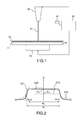
- Figure 1 is a schematic illustration of an electron-beam lithography method and apparatus known from prior art.
- reference 11 corresponds to a substrate - e.g. a silicon wafer or a glass or silica plate - onto which a pattern has to be transferred through direct writing (e.g.
- reference 12 to a resist layer deposed on a surface of said substrate (the term "substrate” will be used indifferently to designate the bare substrate 11 or the ensemble 10 including the resist layer), reference 20 to an electron beam source, reference 21 to an electron beam generated by said source and impinging onto the resist layer 11, reference 30 to an actuation stage for translating the substrate 10 with respect to the electron beam 20, reference 40 to a computer or processor driving the electron beam source 20 and the actuation stage 30, and reference 41 to a computer memory device storing a program executed by said computer or processor 40.
- the electron beam source 20 and the actuation stage 30 cooperate for selectively exposing to the electron beam specific regions of the substrate, according to a predetermined pattern.
- the exposed (positive resist) or the unexposed (negative resist) is selectively eliminated, so that the remaining resist reproduces the predetermined pattern or its complement on the surface of the substrate.
- the portion of the surface of the substrate which is not covered by resist can be etched, and then the remaining resist eliminated.
- Electron beam 21 may be a narrow circular beam, in which case the pattern is projected onto the resist point by point, using raster or vector scanning. In industrial applications, however, it is often preferred to use "shaped beams", which are larger and have a rectangular or triangular section.
- the pattern to be transferred onto the substrate is decomposed into a plurality of elementary features having the shape of the beam. An elementary feature can then be transferred by a single shot - or a series of successive shots for a fixed position of the substrate - with a significant acceleration of the process.
- the dose actually received by the substrate surface does not fall abruptly at the edges of the beam spot, but it decreases smoothly.
- electrons interacting with the resist and/or the substrate experience forward and backward scattering which broadens the dose distribution beyond the theoretical limits of the incident beam spot; in particular, backscattered electrons can travel by a distance of a few micrometers.
- the influence of the interactions of primary electrons with the substrate and the resist on the dose distribution is known as "proximity effects".
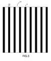
- line 200 illustrates the received dose D distribution across a feature (a line of width W, measured along direction x, and much greater length) of a pattern transferred to a resist layer.
- the received dose D can be obtained by convolving the emitted dose - which may correspond to the design pattern - with a point-spread function representative of the proximity effects.
- the received dose takes a value D 0 at the center of the feature, remains approximately constant across a width W 0 ⁇ W and then decreases smoothly.
- the edges of the transferred feature correspond to the point where the received dose D crosses the energy threshold E Th of the resist.
- the received dose does not go to zero, or it does so slowly, mainly because of forward and backward-scattered electrons coming from the considered feature or adjacent ones.
- increasing the emitted dose increases the width of the feature, and vice-versa.
- an increase of the contribution from backscattered electrons from adjacent features can be compensated by a reduction of the emitted dose (dashed line 203, on the right part of the figure), and vice-versa.
- g(r) is a Gaussian distribution of standard deviation ⁇ b , typically truncated at 3 ⁇ b , taking into account long-range effects (mainly backscattering):
- g r A ⁇ exp - r - r ⁇ 2 / ⁇ b 2
- A is a normalization constant.
- the invention aims at overcoming this drawback of the prior art; more precisely it aims at improving the precision of the received dose modulation on one- and two-dimensional critical shapes (i.e. with narrow width, space or density) without increasing - or even reducing - its implementation complexity.
- An object of the present invention is a method for transferring a pattern onto a substrate by direct writing by means of a particle or photon beam, the method comprising:
- Another object of the invention is a computer program product comprising computer-executable code for causing a computer to produce a dose map, associating an emitted dose to each of a plurality of elementary features of a pattern to be transferred onto a substrate by direct writing by means of a particle or photon beam, by computing at least two metrics for each of said elementary features of the pattern, and determining the emitted dose associated to each of said elementary features of the pattern as a function of said metrics.
- Such a computer program product may further comprise computer-executable code for causing a computer to determine a relation between said metrics and an emitted dose by using numerical simulations or experimental tests to find optimal doses for a plurality of reference patterns, each being representative of a different set of values of said metrics, according to a predetermined optimality criterion.
- Such a computer program product may further comprise computer-executable code for carrying out a method as outlined above by causing a computer to drive a source of said particle or photon beam in order to expose said substrate according to said pattern with a spatially-dependent dose depending on said dose map.
- EBL including variable-shaped beams
- Generalization to vector or raster scan lithography or to other micro- or nano-manufacturing techniques involving particles (not necessarily electrons) or photon beams is straightforward.
- the "elementary features" of the pattern for which the emitted dose has to be calculated are the projections on the substrate of the narrow particle or photon beam.
- the present inventors have realized that the conventional (e.g. Abe's) approach to emitted Dose Modulation is not entirely satisfactory, especially for narrow patterns, because the emitted dose is only computed as a function of the density, and therefore only depends on a "long range" metric, without taking into account local or semi-local features of the pattern.
- the present invention overcomes this limitation by determining the dose as a function of both the density and the critical dimension of each feature.
- the idea at the basis of the invention is the following: an "optimal" dose is computed for each of a plurality of reference patterns, each characterized by a density and a critical dimension (calibration).
- the reference patterns are chosen so that they sample the density - critical dimension plane. This way, a look-up table can be obtained relating (density; critical dimension) pairs to the corresponding optimal exposure doses.
- the look-up table is then used to determine the dose associated to each specific EBL shot, by direct reading or interpolation.
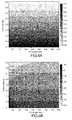
- Figure 3 shows an exemplary reference pattern RP formed by a one-dimensional grating of lines L having a same width and spacing.
- the critical dimension CD corresponds to the width of said lines and the pattern density is calculated using equation 3 above.
- the optimal emitted dose is the one which maximizes the similarity between the reference pattern and the corresponding pattern transferred onto the substrate by EBL. Similarity may be evaluated by comparing the dimensions and/or the contours of the reference and transferred patterns. This optimal emitted dose is determined by trial-and-error, using either detailed physical simulations or actual experiments.
- the density for a point - called point of interest, POI - is determined by computing the convolution of the pattern PT to be transferred onto the substrate with the point spread function of the electron beam, or only its long-range contribution, and by taking the value of said convolution at the POI. It is generally assumed that the point spread function goes to zero beyond a distance of 3 ⁇ b , therefore in practice it is only necessary to take into account the portion of the pattern comprised within a circle of radius 3 ⁇ b centered on the POI.
- FIG. 5 A possible way of doing it is illustrated on figure 5 .
- a series of disks of increasing diameter D1, D2, D3, D4 and D5 and centered on the point of interest are superposed to the pattern.
- the three smallest disks - D1, D2 and D3 - are fully contained within the pattern feature PF containing the point of interest POI (a "pattern feature" is a connected region of the pattern to be transferred, corresponding to a region of the substrate that will be exposed to the electron beam)
- D4 is the smallest disk stretching beyond said feature - and therefore beyond an edge of the pattern, corresponding to the limit of a region of the substrate that will be exposed to the electron beam.
- the critical dimension associated to the point of interest is therefore comprised between the diameters of disks D3 and D4.
- OF 1 1 when the disk is completely contained within a feature of the pattern and OF 1 ⁇ 1 when it stretches beyond the limits of such a feature.
- the POI may be the geometrical center of a shaped spot, constituting an "elementary feature" of the pattern; in general, feature PF is constituted by a plurality of adjacent, or partially overlapping, shots.
- a (density; critical dimension) pair is then associated to each shot.
- the dose associated to a particular (density; critical dimension) pair can be taken equal to the optimal dose for the nearest pair for which an entry of the look-up table exists, the relevant metrics being e.g. a Euclidian distance in the (density - critical dimension) space.
- interpolation e.g. linear, quadratic, spline
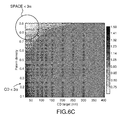
- Figure 6A shows, in grayscale, the emitted dose computed using Abe's formula (equations 1 or 4) for a plurality of reference patterns of the kind of figure 3 , densely sampling the (density - critical dimension) plane. It can be seen that D Abe only depends on the density, and is independent from the critical dimension (and indeed this is apparent from equation 4).
- Figure 6B shows the optimal emitted dose for the same reference patterns, determined by trials and error using numerical simulations, as explained above. It can be seen that, unlike Abe's dose, the optimal emitted dose depends on both critical dimension and density.
- Figure 6C shows the ratio between the optimal dose of figure 6B and the Abe's dose of figure 6A .
- the look-up table could also express the optimal dose as a function of critical dimension and spacing, or of pattern density and spacing, instead of using critical dimension and density. Indeed, the look-up table could be based on any two functions of critical dimension and pattern density (provided they are not simply proportional to each other). It is also possible to take into account additional parameters by using a multidimensional look-up table.
- the inventive method is typically implemented by executing a suitable program on a computer.
- Said computer may directly drive the EBL apparatus (cf. computer or processor 40 on figure 1 ) or simply produce data to be provided to the EBL apparatus.
- the program comprises two main modules: a first one, which receives as an input a fractured pattern (i.e. a pattern decomposed into elementary features corresponding to EBL shots) and computes a critical dimension and a pattern density for each elementary feature of this pattern; and a module that receives said critical dimension and pattern density and uses a pre-computed look-up table to determine and output a dose for each said elementary feature.
- a fractured pattern i.e. a pattern decomposed into elementary features corresponding to EBL shots
- a module that receives said critical dimension and pattern density and uses a pre-computed look-up table to determine and output a dose for each said elementary feature.
- a same program can be able to use different pre-computed look-up tables, corresponding to different processes (a process being defined by a PSF and a resist threshold).
- the program itself and the look-up table(s) may be stored on the same or on different, and possibly remote, computer-readable storage media.
- the program and the look-up table may be stored in the memory device 41 of the processor of figure 1 .
- the program may also include a numerical simulation module and a library of reference patterns for computing the look-up table(s).
- the program may only include the dose map computation module, possibly accompanied by the numerical simulation module, the EBL apparatus being driven by a separate program, receiving the dose map as its input.
- the reference patterns may not necessarily be one-dimensional (i.e. line) gratings; admissible reference patterns may include bi-dimensional gratings (e.g. regular dot patterns, or grids), or even non-grating pattern, e.g. issued from real designs.
- admissible reference patterns may include bi-dimensional gratings (e.g. regular dot patterns, or grids), or even non-grating pattern, e.g. issued from real designs.
- Critical dimension and pattern density are only two of the possible metrics which can be used to compute the optimal emitted dose.
- Other metrics may be used for this purpose, such as SPACE (defined above); other suitable metrics are described in the following papers:
- the optimal emitted dose may be computed as a function a plurality (i.e. two or more) of said metrics.
- a look-up table constitutes a useful tool for representing the relation between a given set of values of the metrics and the corresponding optimal emitted dose, but there are alternatives. For example, it is possible to determine the coefficients of a multi-variable polynomial function expressing the dose as a function of the metrics, storing these coefficients in a computer memory and using them for calculating the optimal emitted dose instead of reading it from a pre-computed table.
- dose modulation may serve other purposes than maximizing the similarity between a reference and a transferred pattern. Said similarity may be ensured using geometry modulation, and dose modulation may then be used to optimize other suitable criteria - i.e. for reducing the exposition time, minimizing the simulation error, reducing the roughness of the edges of the transferred pattern features, etc.
Landscapes
- Chemical & Material Sciences (AREA)
- Analytical Chemistry (AREA)
- Electron Beam Exposure (AREA)
Priority Applications (7)
| Application Number | Priority Date | Filing Date | Title |
|---|---|---|---|
| EP15306181.7A EP3121833A1 (fr) | 2015-07-20 | 2015-07-20 | Procédé permettant d'effectuer une modulation de dose, notamment pour la lithographie par faisceau d'électrons |
| US15/742,003 US10522328B2 (en) | 2015-07-20 | 2016-07-19 | Method of performing dose modulation, in particular for electron beam lithography |
| PCT/EP2016/067112 WO2017013085A1 (fr) | 2015-07-20 | 2016-07-19 | Procédé de réalisation de modulation de dose, en particulier pour la lithographie à faisceau d'électrons |
| JP2018502649A JP6564932B2 (ja) | 2015-07-20 | 2016-07-19 | 特に電子ビームリソグラフィのために線量変調を実行する方法 |
| KR1020187001618A KR102033862B1 (ko) | 2015-07-20 | 2016-07-19 | 전자 빔 리소그래피를 위해 선량 변조를 수행하는 방법 |
| TW105122756A TWI622079B (zh) | 2015-07-20 | 2016-07-19 | 執行劑量調變之方法,特別是用於電子束微影 |
| EP16744685.5A EP3326192A1 (fr) | 2015-07-20 | 2016-07-19 | Procédé de réalisation de modulation de dose, en particulier pour la lithographie à faisceau d'électrons |
Applications Claiming Priority (1)
| Application Number | Priority Date | Filing Date | Title |
|---|---|---|---|
| EP15306181.7A EP3121833A1 (fr) | 2015-07-20 | 2015-07-20 | Procédé permettant d'effectuer une modulation de dose, notamment pour la lithographie par faisceau d'électrons |
Publications (1)
| Publication Number | Publication Date |
|---|---|
| EP3121833A1 true EP3121833A1 (fr) | 2017-01-25 |
Family
ID=53758156
Family Applications (2)
| Application Number | Title | Priority Date | Filing Date |
|---|---|---|---|
| EP15306181.7A Withdrawn EP3121833A1 (fr) | 2015-07-20 | 2015-07-20 | Procédé permettant d'effectuer une modulation de dose, notamment pour la lithographie par faisceau d'électrons |
| EP16744685.5A Pending EP3326192A1 (fr) | 2015-07-20 | 2016-07-19 | Procédé de réalisation de modulation de dose, en particulier pour la lithographie à faisceau d'électrons |
Family Applications After (1)
| Application Number | Title | Priority Date | Filing Date |
|---|---|---|---|
| EP16744685.5A Pending EP3326192A1 (fr) | 2015-07-20 | 2016-07-19 | Procédé de réalisation de modulation de dose, en particulier pour la lithographie à faisceau d'électrons |
Country Status (6)
| Country | Link |
|---|---|
| US (1) | US10522328B2 (fr) |
| EP (2) | EP3121833A1 (fr) |
| JP (1) | JP6564932B2 (fr) |
| KR (1) | KR102033862B1 (fr) |
| TW (1) | TWI622079B (fr) |
| WO (1) | WO2017013085A1 (fr) |
Cited By (1)
| Publication number | Priority date | Publication date | Assignee | Title |
|---|---|---|---|---|
| FR3068148A1 (fr) * | 2017-06-27 | 2018-12-28 | Commissariat A L'energie Atomique Et Aux Energies Alternatives | Etalonnage de petits motifs elementaires en lithographie electronique a faisceau forme |
Families Citing this family (7)
| Publication number | Priority date | Publication date | Assignee | Title |
|---|---|---|---|---|
| JP7031516B2 (ja) * | 2018-07-06 | 2022-03-08 | 株式会社ニューフレアテクノロジー | 照射量補正量の取得方法、荷電粒子ビーム描画方法、及び荷電粒子ビーム描画装置 |
| US20230124768A1 (en) | 2019-05-24 | 2023-04-20 | D2S, Inc. | Method and system for determining a charged particle beam exposure for a local pattern density |
| US10748744B1 (en) * | 2019-05-24 | 2020-08-18 | D2S, Inc. | Method and system for determining a charged particle beam exposure for a local pattern density |
| US10921716B1 (en) | 2019-10-08 | 2021-02-16 | International Business Machines Corporation | Lithographic dose characterization |
| CN111965936B (zh) * | 2020-09-27 | 2022-06-07 | 湖南大学 | 大规模电子束曝光版图的高精度邻近效应快速矫正方法 |
| CN119156686A (zh) * | 2022-05-13 | 2024-12-17 | 应用材料公司 | 使用基板曲率来进行剂量绘图以补偿平面外畸变 |
| KR20250008925A (ko) * | 2022-05-13 | 2025-01-16 | 어플라이드 머티어리얼스, 인코포레이티드 | 개선된 분해능을 갖는 기판 곡률 제어용 도즈 매핑 및 기판 회전 |
Citations (5)
| Publication number | Priority date | Publication date | Assignee | Title |
|---|---|---|---|---|
| FR1157338A (fr) | 1955-07-12 | 1958-05-28 | Courtaulds Ltd | Perfectionnements à la fabrication de filaments, fils, fibres et produits similaires à partir de viscose |
| FR1253389A (fr) | 1959-12-22 | 1961-02-10 | Thompson Ramo Wooldridge Inc | Circuit de charge à courant constant |
| US20070228293A1 (en) * | 2002-02-08 | 2007-10-04 | Kabushiki Kaisha Toshiba | Pattern writing and forming method |
| JP2012212792A (ja) * | 2011-03-31 | 2012-11-01 | Nuflare Technology Inc | 荷電粒子ビーム描画装置及び荷電粒子ビーム描画方法 |
| US20140077103A1 (en) * | 2012-09-14 | 2014-03-20 | Nuflare Technology, Inc. | Charged particle beam writing apparatus and charged particle beam writing method |
Family Cites Families (12)
| Publication number | Priority date | Publication date | Assignee | Title |
|---|---|---|---|---|
| JP2003264140A (ja) * | 2002-03-11 | 2003-09-19 | Nikon Corp | 荷電粒子線露光装置におけるeid関数の近似方法、近接効果補正方法、及びレチクルパターンの決定方法 |
| US7266800B2 (en) * | 2004-06-04 | 2007-09-04 | Invarium, Inc. | Method and system for designing manufacturable patterns that account for the pattern- and position-dependent nature of patterning processes |
| JP2007115999A (ja) * | 2005-10-21 | 2007-05-10 | Toshiba Corp | キャラクタプロジェクション(cp)方式の荷電粒子ビーム露光方法、キャラクタプロジェクション方式の荷電粒子ビーム露光装置及びプログラム |
| US8120767B2 (en) * | 2008-03-13 | 2012-02-21 | Taiwan Semiconductor Manufacturing Company, Ltd. | Mask making decision for manufacturing (DFM) on mask quality control |
| KR101828108B1 (ko) * | 2010-09-17 | 2018-02-09 | 니폰 컨트롤 시스템 가부시키가이샤 | 묘화방법 및 묘화장치 |
| JP2014029888A (ja) * | 2010-10-12 | 2014-02-13 | Nippon Control System Corporation | 描画方法及び描画装置、並びにプログラム |
| FR2979165B1 (fr) | 2011-08-16 | 2014-05-16 | Commissariat Energie Atomique | Procede de correction des effets de proximite electronique utilisant des fonctions de diffusion decentrees |
| FR2989513B1 (fr) | 2012-04-12 | 2015-04-17 | Aselta Nanographics | Procede de correction des effets de proximite electronique utilisant des fonctions de diffusion de type voigt |
| FR2994749B1 (fr) * | 2012-08-24 | 2015-07-24 | Commissariat Energie Atomique | Procede de preparation d’un motif a imprimer sur plaque ou sur masque par lithographie a faisceau d’electrons, systeme de conception de circuit imprime et programme d’ordinateur correspondants. |
| EP2869119A1 (fr) * | 2013-10-30 | 2015-05-06 | Aselta Nanographics | Procédé de fracturation de forme libre pour lithographie électronique ou optique utilisant le contrôle du seuil d'activation de la résine photosensible |
| EP2952963B1 (fr) | 2014-06-03 | 2020-12-30 | Commissariat A L'energie Atomique Et Aux Energies Alternatives | Procédé pour calculer les paramètres d'un procédé de fabrication de circuits intégrés |
| EP2983193B1 (fr) * | 2014-08-05 | 2021-10-20 | Aselta Nanographics | Procédé pour déterminer les paramètres d'un modèle de processus de fabrication de circuits intégrés |
-
2015
- 2015-07-20 EP EP15306181.7A patent/EP3121833A1/fr not_active Withdrawn
-
2016
- 2016-07-19 WO PCT/EP2016/067112 patent/WO2017013085A1/fr not_active Ceased
- 2016-07-19 JP JP2018502649A patent/JP6564932B2/ja active Active
- 2016-07-19 EP EP16744685.5A patent/EP3326192A1/fr active Pending
- 2016-07-19 US US15/742,003 patent/US10522328B2/en active Active
- 2016-07-19 KR KR1020187001618A patent/KR102033862B1/ko active Active
- 2016-07-19 TW TW105122756A patent/TWI622079B/zh active
Patent Citations (5)
| Publication number | Priority date | Publication date | Assignee | Title |
|---|---|---|---|---|
| FR1157338A (fr) | 1955-07-12 | 1958-05-28 | Courtaulds Ltd | Perfectionnements à la fabrication de filaments, fils, fibres et produits similaires à partir de viscose |
| FR1253389A (fr) | 1959-12-22 | 1961-02-10 | Thompson Ramo Wooldridge Inc | Circuit de charge à courant constant |
| US20070228293A1 (en) * | 2002-02-08 | 2007-10-04 | Kabushiki Kaisha Toshiba | Pattern writing and forming method |
| JP2012212792A (ja) * | 2011-03-31 | 2012-11-01 | Nuflare Technology Inc | 荷電粒子ビーム描画装置及び荷電粒子ビーム描画方法 |
| US20140077103A1 (en) * | 2012-09-14 | 2014-03-20 | Nuflare Technology, Inc. | Charged particle beam writing apparatus and charged particle beam writing method |
Non-Patent Citations (4)
| Title |
|---|
| DATABASE EPODOC [online] EUROPEAN PATENT OFFICE, THE HAGUE, NL; 1 November 2012 (2012-11-01), XP055243313, Database accession no. JP-2011077810-A * |
| J.-G. PARK; S.-W. KIM; S.-B. SHIM; S.-S. SUH; H.-K. OH: "The effective etch process proximity correction methodology for improving on chip CD variation in 20 nm node DRAM gate", DESIGN FOR MANUFACTURABILITY THOUGH DESIGN-PROCESS INTEGRATION V, PROC. SPIE, vol. 7974, 2011 |
| S. SATO; K. OZAWA; F. UESAWA: "Dry-etch proximity function for model-based OPC beyond 65-nm node", PROC. SPIE, vol. 6155, 2006 |
| TAKAYUKI ABE ET AL.: "High-Accuracy Proximity Effect Correction for Mask Writing", JAPANESE JOURNAL OF APPLIED PHYSICS, vol. 46, no. 2, 2007, pages 826 - 833 |
Cited By (5)
| Publication number | Priority date | Publication date | Assignee | Title |
|---|---|---|---|---|
| FR3068148A1 (fr) * | 2017-06-27 | 2018-12-28 | Commissariat A L'energie Atomique Et Aux Energies Alternatives | Etalonnage de petits motifs elementaires en lithographie electronique a faisceau forme |
| EP3422387A1 (fr) * | 2017-06-27 | 2019-01-02 | Commissariat à l'Energie Atomique et aux Energies Alternatives | Etalonnage de petits motifs elementaires en lithographie electronique a faisceau forme |
| KR20190001571A (ko) * | 2017-06-27 | 2019-01-04 | 꼼미사리아 아 레네르지 아토미끄 에뜨 옥스 에너지스 앨터네이티브즈 | 가변 형상 빔 전자 빔 리소그래피에서의 기본 작은 패턴의 교정 |
| US10573492B2 (en) | 2017-06-27 | 2020-02-25 | Commissariat A L'energie Atomique Et Aux Energies Alternatives | Calibration of elementary small patterns in variable-shaped-beam electron-beam lithography |
| KR102546380B1 (ko) | 2017-06-27 | 2023-06-21 | 꼼미사리아 아 레네르지 아토미끄 에뜨 옥스 에너지스 앨터네이티브즈 | 가변 형상 빔 전자 빔 리소그래피에서의 기본 작은 패턴의 교정 |
Also Published As
| Publication number | Publication date |
|---|---|
| WO2017013085A1 (fr) | 2017-01-26 |
| KR20180107071A (ko) | 2018-10-01 |
| JP6564932B2 (ja) | 2019-08-21 |
| TWI622079B (zh) | 2018-04-21 |
| TW201717244A (zh) | 2017-05-16 |
| US10522328B2 (en) | 2019-12-31 |
| KR102033862B1 (ko) | 2019-10-17 |
| EP3326192A1 (fr) | 2018-05-30 |
| US20180204707A1 (en) | 2018-07-19 |
| JP2018524818A (ja) | 2018-08-30 |
Similar Documents
| Publication | Publication Date | Title |
|---|---|---|
| US10522328B2 (en) | Method of performing dose modulation, in particular for electron beam lithography | |
| KR102154105B1 (ko) | 하전 입자 빔 리소그라피를 이용하여 패턴들을 형성하기 위한 방법 및 시스템 | |
| JP4476975B2 (ja) | 荷電粒子ビーム照射量演算方法、荷電粒子ビーム描画方法、プログラム及び荷電粒子ビーム描画装置 | |
| JP5480555B2 (ja) | 荷電粒子ビーム描画装置及び荷電粒子ビーム描画方法 | |
| US8285030B2 (en) | Determining calibration parameters for a lithographic process | |
| KR101711699B1 (ko) | 마스크 패턴 작성 방법, 기록 매체 및 정보 처리 장치 | |
| US20130346037A1 (en) | Lithography Modeling And Applications | |
| JP2007507891A (ja) | リソグラフィシミュレーションのための装置および方法 | |
| US10423074B2 (en) | Method for calculating the metrics of an IC manufacturing process | |
| JP2009139632A (ja) | マスクパターン補正方法及び露光用マスク | |
| US10295912B2 (en) | Method for determining the parameters of an IC manufacturing process model | |
| US10156796B2 (en) | Method for determining the parameters of an IC manufacturing process by a differential procedure | |
| US9934336B2 (en) | Method of correcting electron proximity effects using Voigt type scattering functions | |
| JP5416998B2 (ja) | 荷電粒子ビーム描画方法および荷電粒子ビーム描画装置 | |
| JP2010225811A (ja) | 荷電粒子ビーム描画方法 | |
| JP6167663B2 (ja) | 現像ローディング補正プログラム、計算機、描画システム、現像ローディング補正方法 | |
| EP4495975A1 (fr) | Détermination de la fonction de transfert d'imagerie d'un appareil d'exposition à particules chargées à l'aide de mesures de dose isofocales | |
| US20260104649A1 (en) | Optical proximity correction (opc) method based on deep learning | |
| JP2010147449A (ja) | 荷電粒子ビーム描画方法および荷電粒子ビーム描画装置 | |
| KR20190018638A (ko) | 산란 효과들의 수정에 의해 기판 상으로의 입자들의 빔을 투사하기 위한 방법 | |
| JP2013156451A (ja) | 露光方法 |
Legal Events
| Date | Code | Title | Description |
|---|---|---|---|
| PUAI | Public reference made under article 153(3) epc to a published international application that has entered the european phase |
Free format text: ORIGINAL CODE: 0009012 |
|
| AK | Designated contracting states |
Kind code of ref document: A1 Designated state(s): AL AT BE BG CH CY CZ DE DK EE ES FI FR GB GR HR HU IE IS IT LI LT LU LV MC MK MT NL NO PL PT RO RS SE SI SK SM TR |
|
| AX | Request for extension of the european patent |
Extension state: BA ME |
|
| STAA | Information on the status of an ep patent application or granted ep patent |
Free format text: STATUS: THE APPLICATION IS DEEMED TO BE WITHDRAWN |
|
| 18D | Application deemed to be withdrawn |
Effective date: 20170726 |